US9484264B1 - Field effect transistor contacts - Google Patents
Field effect transistor contacts Download PDFInfo
- Publication number
- US9484264B1 US9484264B1 US14/812,330 US201514812330A US9484264B1 US 9484264 B1 US9484264 B1 US 9484264B1 US 201514812330 A US201514812330 A US 201514812330A US 9484264 B1 US9484264 B1 US 9484264B1
- Authority
- US
- United States
- Prior art keywords
- fin
- width
- gate stack
- substrate
- contacts
- Prior art date
- Legal status (The legal status is an assumption and is not a legal conclusion. Google has not performed a legal analysis and makes no representation as to the accuracy of the status listed.)
- Expired - Fee Related
Links
- 230000005669 field effect Effects 0.000 title claims abstract description 12
- 239000000758 substrate Substances 0.000 claims abstract description 21
- 239000000463 material Substances 0.000 claims description 31
- 239000012212 insulator Substances 0.000 claims description 19
- 239000004065 semiconductor Substances 0.000 claims description 6
- 239000007769 metal material Substances 0.000 claims description 2
- 239000004020 conductor Substances 0.000 abstract description 12
- 238000000034 method Methods 0.000 description 28
- 238000005530 etching Methods 0.000 description 10
- 238000000151 deposition Methods 0.000 description 6
- 238000000059 patterning Methods 0.000 description 6
- 238000001020 plasma etching Methods 0.000 description 6
- 125000006850 spacer group Chemical group 0.000 description 6
- 230000015572 biosynthetic process Effects 0.000 description 4
- 229910052751 metal Inorganic materials 0.000 description 3
- 239000002184 metal Substances 0.000 description 3
- 150000004767 nitrides Chemical class 0.000 description 3
- 230000008021 deposition Effects 0.000 description 2
- 238000010586 diagram Methods 0.000 description 2
- 238000001459 lithography Methods 0.000 description 2
- 230000000873 masking effect Effects 0.000 description 2
- 238000012986 modification Methods 0.000 description 2
- 230000004048 modification Effects 0.000 description 2
- 229910021332 silicide Inorganic materials 0.000 description 2
- FVBUAEGBCNSCDD-UHFFFAOYSA-N silicide(4-) Chemical compound [Si-4] FVBUAEGBCNSCDD-UHFFFAOYSA-N 0.000 description 2
- RYGMFSIKBFXOCR-UHFFFAOYSA-N Copper Chemical compound [Cu] RYGMFSIKBFXOCR-UHFFFAOYSA-N 0.000 description 1
- 229910052581 Si3N4 Inorganic materials 0.000 description 1
- BQCADISMDOOEFD-UHFFFAOYSA-N Silver Chemical compound [Ag] BQCADISMDOOEFD-UHFFFAOYSA-N 0.000 description 1
- 229910052782 aluminium Inorganic materials 0.000 description 1
- XAGFODPZIPBFFR-UHFFFAOYSA-N aluminium Chemical compound [Al] XAGFODPZIPBFFR-UHFFFAOYSA-N 0.000 description 1
- 238000004380 ashing Methods 0.000 description 1
- QVGXLLKOCUKJST-UHFFFAOYSA-N atomic oxygen Chemical compound [O] QVGXLLKOCUKJST-UHFFFAOYSA-N 0.000 description 1
- 229910052802 copper Inorganic materials 0.000 description 1
- 239000010949 copper Substances 0.000 description 1
- 239000002019 doping agent Substances 0.000 description 1
- 238000004519 manufacturing process Methods 0.000 description 1
- 229910052758 niobium Inorganic materials 0.000 description 1
- 239000010955 niobium Substances 0.000 description 1
- GUCVJGMIXFAOAE-UHFFFAOYSA-N niobium atom Chemical compound [Nb] GUCVJGMIXFAOAE-UHFFFAOYSA-N 0.000 description 1
- 239000011368 organic material Substances 0.000 description 1
- 229910052760 oxygen Inorganic materials 0.000 description 1
- 239000001301 oxygen Substances 0.000 description 1
- 238000005498 polishing Methods 0.000 description 1
- HQVNEWCFYHHQES-UHFFFAOYSA-N silicon nitride Chemical compound N12[Si]34N5[Si]62N3[Si]51N64 HQVNEWCFYHHQES-UHFFFAOYSA-N 0.000 description 1
- 239000002210 silicon-based material Substances 0.000 description 1
- 229910052709 silver Inorganic materials 0.000 description 1
- 239000004332 silver Substances 0.000 description 1
- 239000000126 substance Substances 0.000 description 1
- 229910052715 tantalum Inorganic materials 0.000 description 1
- GUVRBAGPIYLISA-UHFFFAOYSA-N tantalum atom Chemical compound [Ta] GUVRBAGPIYLISA-UHFFFAOYSA-N 0.000 description 1
- MZLGASXMSKOWSE-UHFFFAOYSA-N tantalum nitride Chemical compound [Ta]#N MZLGASXMSKOWSE-UHFFFAOYSA-N 0.000 description 1
- WFKWXMTUELFFGS-UHFFFAOYSA-N tungsten Chemical compound [W] WFKWXMTUELFFGS-UHFFFAOYSA-N 0.000 description 1
- 229910052721 tungsten Inorganic materials 0.000 description 1
- 239000010937 tungsten Substances 0.000 description 1
Images


Classifications
-
- H—ELECTRICITY
- H01—ELECTRIC ELEMENTS
- H01L—SEMICONDUCTOR DEVICES NOT COVERED BY CLASS H10
- H01L21/00—Processes or apparatus adapted for the manufacture or treatment of semiconductor or solid state devices or of parts thereof
- H01L21/70—Manufacture or treatment of devices consisting of a plurality of solid state components formed in or on a common substrate or of parts thereof; Manufacture of integrated circuit devices or of parts thereof
- H01L21/77—Manufacture or treatment of devices consisting of a plurality of solid state components or integrated circuits formed in, or on, a common substrate
- H01L21/78—Manufacture or treatment of devices consisting of a plurality of solid state components or integrated circuits formed in, or on, a common substrate with subsequent division of the substrate into plural individual devices
- H01L21/82—Manufacture or treatment of devices consisting of a plurality of solid state components or integrated circuits formed in, or on, a common substrate with subsequent division of the substrate into plural individual devices to produce devices, e.g. integrated circuits, each consisting of a plurality of components
- H01L21/822—Manufacture or treatment of devices consisting of a plurality of solid state components or integrated circuits formed in, or on, a common substrate with subsequent division of the substrate into plural individual devices to produce devices, e.g. integrated circuits, each consisting of a plurality of components the substrate being a semiconductor, using silicon technology
- H01L21/8232—Field-effect technology
- H01L21/8234—MIS technology, i.e. integration processes of field effect transistors of the conductor-insulator-semiconductor type
- H01L21/823437—MIS technology, i.e. integration processes of field effect transistors of the conductor-insulator-semiconductor type with a particular manufacturing method of the gate conductors, e.g. particular materials, shapes
-
- H—ELECTRICITY
- H01—ELECTRIC ELEMENTS
- H01L—SEMICONDUCTOR DEVICES NOT COVERED BY CLASS H10
- H01L21/00—Processes or apparatus adapted for the manufacture or treatment of semiconductor or solid state devices or of parts thereof
- H01L21/02—Manufacture or treatment of semiconductor devices or of parts thereof
- H01L21/04—Manufacture or treatment of semiconductor devices or of parts thereof the devices having potential barriers, e.g. a PN junction, depletion layer or carrier concentration layer
- H01L21/18—Manufacture or treatment of semiconductor devices or of parts thereof the devices having potential barriers, e.g. a PN junction, depletion layer or carrier concentration layer the devices having semiconductor bodies comprising elements of Group IV of the Periodic Table or AIIIBV compounds with or without impurities, e.g. doping materials
- H01L21/30—Treatment of semiconductor bodies using processes or apparatus not provided for in groups H01L21/20 - H01L21/26
- H01L21/31—Treatment of semiconductor bodies using processes or apparatus not provided for in groups H01L21/20 - H01L21/26 to form insulating layers thereon, e.g. for masking or by using photolithographic techniques; After treatment of these layers; Selection of materials for these layers
- H01L21/3105—After-treatment
- H01L21/311—Etching the insulating layers by chemical or physical means
- H01L21/31144—Etching the insulating layers by chemical or physical means using masks
-
- H—ELECTRICITY
- H01—ELECTRIC ELEMENTS
- H01L—SEMICONDUCTOR DEVICES NOT COVERED BY CLASS H10
- H01L21/00—Processes or apparatus adapted for the manufacture or treatment of semiconductor or solid state devices or of parts thereof
- H01L21/70—Manufacture or treatment of devices consisting of a plurality of solid state components formed in or on a common substrate or of parts thereof; Manufacture of integrated circuit devices or of parts thereof
- H01L21/71—Manufacture of specific parts of devices defined in group H01L21/70
- H01L21/768—Applying interconnections to be used for carrying current between separate components within a device comprising conductors and dielectrics
- H01L21/76801—Applying interconnections to be used for carrying current between separate components within a device comprising conductors and dielectrics characterised by the formation and the after-treatment of the dielectrics, e.g. smoothing
- H01L21/76802—Applying interconnections to be used for carrying current between separate components within a device comprising conductors and dielectrics characterised by the formation and the after-treatment of the dielectrics, e.g. smoothing by forming openings in dielectrics
- H01L21/76816—Aspects relating to the layout of the pattern or to the size of vias or trenches
-
- H—ELECTRICITY
- H01—ELECTRIC ELEMENTS
- H01L—SEMICONDUCTOR DEVICES NOT COVERED BY CLASS H10
- H01L21/00—Processes or apparatus adapted for the manufacture or treatment of semiconductor or solid state devices or of parts thereof
- H01L21/70—Manufacture or treatment of devices consisting of a plurality of solid state components formed in or on a common substrate or of parts thereof; Manufacture of integrated circuit devices or of parts thereof
- H01L21/71—Manufacture of specific parts of devices defined in group H01L21/70
- H01L21/768—Applying interconnections to be used for carrying current between separate components within a device comprising conductors and dielectrics
- H01L21/76838—Applying interconnections to be used for carrying current between separate components within a device comprising conductors and dielectrics characterised by the formation and the after-treatment of the conductors
- H01L21/7684—Smoothing; Planarisation
-
- H—ELECTRICITY
- H01—ELECTRIC ELEMENTS
- H01L—SEMICONDUCTOR DEVICES NOT COVERED BY CLASS H10
- H01L21/00—Processes or apparatus adapted for the manufacture or treatment of semiconductor or solid state devices or of parts thereof
- H01L21/70—Manufacture or treatment of devices consisting of a plurality of solid state components formed in or on a common substrate or of parts thereof; Manufacture of integrated circuit devices or of parts thereof
- H01L21/71—Manufacture of specific parts of devices defined in group H01L21/70
- H01L21/768—Applying interconnections to be used for carrying current between separate components within a device comprising conductors and dielectrics
- H01L21/76838—Applying interconnections to be used for carrying current between separate components within a device comprising conductors and dielectrics characterised by the formation and the after-treatment of the conductors
- H01L21/76877—Filling of holes, grooves or trenches, e.g. vias, with conductive material
-
- H—ELECTRICITY
- H01—ELECTRIC ELEMENTS
- H01L—SEMICONDUCTOR DEVICES NOT COVERED BY CLASS H10
- H01L21/00—Processes or apparatus adapted for the manufacture or treatment of semiconductor or solid state devices or of parts thereof
- H01L21/70—Manufacture or treatment of devices consisting of a plurality of solid state components formed in or on a common substrate or of parts thereof; Manufacture of integrated circuit devices or of parts thereof
- H01L21/71—Manufacture of specific parts of devices defined in group H01L21/70
- H01L21/768—Applying interconnections to be used for carrying current between separate components within a device comprising conductors and dielectrics
- H01L21/76897—Formation of self-aligned vias or contact plugs, i.e. involving a lithographically uncritical step
-
- H—ELECTRICITY
- H01—ELECTRIC ELEMENTS
- H01L—SEMICONDUCTOR DEVICES NOT COVERED BY CLASS H10
- H01L21/00—Processes or apparatus adapted for the manufacture or treatment of semiconductor or solid state devices or of parts thereof
- H01L21/70—Manufacture or treatment of devices consisting of a plurality of solid state components formed in or on a common substrate or of parts thereof; Manufacture of integrated circuit devices or of parts thereof
- H01L21/77—Manufacture or treatment of devices consisting of a plurality of solid state components or integrated circuits formed in, or on, a common substrate
- H01L21/78—Manufacture or treatment of devices consisting of a plurality of solid state components or integrated circuits formed in, or on, a common substrate with subsequent division of the substrate into plural individual devices
- H01L21/82—Manufacture or treatment of devices consisting of a plurality of solid state components or integrated circuits formed in, or on, a common substrate with subsequent division of the substrate into plural individual devices to produce devices, e.g. integrated circuits, each consisting of a plurality of components
- H01L21/822—Manufacture or treatment of devices consisting of a plurality of solid state components or integrated circuits formed in, or on, a common substrate with subsequent division of the substrate into plural individual devices to produce devices, e.g. integrated circuits, each consisting of a plurality of components the substrate being a semiconductor, using silicon technology
- H01L21/8232—Field-effect technology
- H01L21/8234—MIS technology, i.e. integration processes of field effect transistors of the conductor-insulator-semiconductor type
- H01L21/823431—MIS technology, i.e. integration processes of field effect transistors of the conductor-insulator-semiconductor type with a particular manufacturing method of transistors with a horizontal current flow in a vertical sidewall of a semiconductor body, e.g. FinFET, MuGFET
-
- H—ELECTRICITY
- H01—ELECTRIC ELEMENTS
- H01L—SEMICONDUCTOR DEVICES NOT COVERED BY CLASS H10
- H01L21/00—Processes or apparatus adapted for the manufacture or treatment of semiconductor or solid state devices or of parts thereof
- H01L21/70—Manufacture or treatment of devices consisting of a plurality of solid state components formed in or on a common substrate or of parts thereof; Manufacture of integrated circuit devices or of parts thereof
- H01L21/77—Manufacture or treatment of devices consisting of a plurality of solid state components or integrated circuits formed in, or on, a common substrate
- H01L21/78—Manufacture or treatment of devices consisting of a plurality of solid state components or integrated circuits formed in, or on, a common substrate with subsequent division of the substrate into plural individual devices
- H01L21/82—Manufacture or treatment of devices consisting of a plurality of solid state components or integrated circuits formed in, or on, a common substrate with subsequent division of the substrate into plural individual devices to produce devices, e.g. integrated circuits, each consisting of a plurality of components
- H01L21/822—Manufacture or treatment of devices consisting of a plurality of solid state components or integrated circuits formed in, or on, a common substrate with subsequent division of the substrate into plural individual devices to produce devices, e.g. integrated circuits, each consisting of a plurality of components the substrate being a semiconductor, using silicon technology
- H01L21/8232—Field-effect technology
- H01L21/8234—MIS technology, i.e. integration processes of field effect transistors of the conductor-insulator-semiconductor type
- H01L21/823475—MIS technology, i.e. integration processes of field effect transistors of the conductor-insulator-semiconductor type interconnection or wiring or contact manufacturing related aspects
-
- H—ELECTRICITY
- H01—ELECTRIC ELEMENTS
- H01L—SEMICONDUCTOR DEVICES NOT COVERED BY CLASS H10
- H01L27/00—Devices consisting of a plurality of semiconductor or other solid-state components formed in or on a common substrate
- H01L27/02—Devices consisting of a plurality of semiconductor or other solid-state components formed in or on a common substrate including semiconductor components specially adapted for rectifying, oscillating, amplifying or switching and having potential barriers; including integrated passive circuit elements having potential barriers
- H01L27/04—Devices consisting of a plurality of semiconductor or other solid-state components formed in or on a common substrate including semiconductor components specially adapted for rectifying, oscillating, amplifying or switching and having potential barriers; including integrated passive circuit elements having potential barriers the substrate being a semiconductor body
- H01L27/08—Devices consisting of a plurality of semiconductor or other solid-state components formed in or on a common substrate including semiconductor components specially adapted for rectifying, oscillating, amplifying or switching and having potential barriers; including integrated passive circuit elements having potential barriers the substrate being a semiconductor body including only semiconductor components of a single kind
- H01L27/085—Devices consisting of a plurality of semiconductor or other solid-state components formed in or on a common substrate including semiconductor components specially adapted for rectifying, oscillating, amplifying or switching and having potential barriers; including integrated passive circuit elements having potential barriers the substrate being a semiconductor body including only semiconductor components of a single kind including field-effect components only
- H01L27/088—Devices consisting of a plurality of semiconductor or other solid-state components formed in or on a common substrate including semiconductor components specially adapted for rectifying, oscillating, amplifying or switching and having potential barriers; including integrated passive circuit elements having potential barriers the substrate being a semiconductor body including only semiconductor components of a single kind including field-effect components only the components being field-effect transistors with insulated gate
- H01L27/0886—Devices consisting of a plurality of semiconductor or other solid-state components formed in or on a common substrate including semiconductor components specially adapted for rectifying, oscillating, amplifying or switching and having potential barriers; including integrated passive circuit elements having potential barriers the substrate being a semiconductor body including only semiconductor components of a single kind including field-effect components only the components being field-effect transistors with insulated gate including transistors with a horizontal current flow in a vertical sidewall of a semiconductor body, e.g. FinFET, MuGFET
-
- H—ELECTRICITY
- H01—ELECTRIC ELEMENTS
- H01L—SEMICONDUCTOR DEVICES NOT COVERED BY CLASS H10
- H01L29/00—Semiconductor devices specially adapted for rectifying, amplifying, oscillating or switching and having potential barriers; Capacitors or resistors having potential barriers, e.g. a PN-junction depletion layer or carrier concentration layer; Details of semiconductor bodies or of electrodes thereof ; Multistep manufacturing processes therefor
- H01L29/02—Semiconductor bodies ; Multistep manufacturing processes therefor
- H01L29/06—Semiconductor bodies ; Multistep manufacturing processes therefor characterised by their shape; characterised by the shapes, relative sizes, or dispositions of the semiconductor regions ; characterised by the concentration or distribution of impurities within semiconductor regions
- H01L29/0603—Semiconductor bodies ; Multistep manufacturing processes therefor characterised by their shape; characterised by the shapes, relative sizes, or dispositions of the semiconductor regions ; characterised by the concentration or distribution of impurities within semiconductor regions characterised by particular constructional design considerations, e.g. for preventing surface leakage, for controlling electric field concentration or for internal isolations regions
- H01L29/0642—Isolation within the component, i.e. internal isolation
-
- H—ELECTRICITY
- H01—ELECTRIC ELEMENTS
- H01L—SEMICONDUCTOR DEVICES NOT COVERED BY CLASS H10
- H01L29/00—Semiconductor devices specially adapted for rectifying, amplifying, oscillating or switching and having potential barriers; Capacitors or resistors having potential barriers, e.g. a PN-junction depletion layer or carrier concentration layer; Details of semiconductor bodies or of electrodes thereof ; Multistep manufacturing processes therefor
- H01L29/40—Electrodes ; Multistep manufacturing processes therefor
- H01L29/43—Electrodes ; Multistep manufacturing processes therefor characterised by the materials of which they are formed
- H01L29/49—Metal-insulator-semiconductor electrodes, e.g. gates of MOSFET
- H01L29/495—Metal-insulator-semiconductor electrodes, e.g. gates of MOSFET the conductor material next to the insulator being a simple metal, e.g. W, Mo
-
- H—ELECTRICITY
- H01—ELECTRIC ELEMENTS
- H01L—SEMICONDUCTOR DEVICES NOT COVERED BY CLASS H10
- H01L29/00—Semiconductor devices specially adapted for rectifying, amplifying, oscillating or switching and having potential barriers; Capacitors or resistors having potential barriers, e.g. a PN-junction depletion layer or carrier concentration layer; Details of semiconductor bodies or of electrodes thereof ; Multistep manufacturing processes therefor
- H01L29/40—Electrodes ; Multistep manufacturing processes therefor
- H01L29/43—Electrodes ; Multistep manufacturing processes therefor characterised by the materials of which they are formed
- H01L29/49—Metal-insulator-semiconductor electrodes, e.g. gates of MOSFET
- H01L29/4966—Metal-insulator-semiconductor electrodes, e.g. gates of MOSFET the conductor material next to the insulator being a composite material, e.g. organic material, TiN, MoSi2
-
- H—ELECTRICITY
- H01—ELECTRIC ELEMENTS
- H01L—SEMICONDUCTOR DEVICES NOT COVERED BY CLASS H10
- H01L29/00—Semiconductor devices specially adapted for rectifying, amplifying, oscillating or switching and having potential barriers; Capacitors or resistors having potential barriers, e.g. a PN-junction depletion layer or carrier concentration layer; Details of semiconductor bodies or of electrodes thereof ; Multistep manufacturing processes therefor
- H01L29/66—Types of semiconductor device ; Multistep manufacturing processes therefor
- H01L29/66007—Multistep manufacturing processes
- H01L29/66075—Multistep manufacturing processes of devices having semiconductor bodies comprising group 14 or group 13/15 materials
- H01L29/66227—Multistep manufacturing processes of devices having semiconductor bodies comprising group 14 or group 13/15 materials the devices being controllable only by the electric current supplied or the electric potential applied, to an electrode which does not carry the current to be rectified, amplified or switched, e.g. three-terminal devices
- H01L29/66409—Unipolar field-effect transistors
- H01L29/66848—Unipolar field-effect transistors with a Schottky gate, i.e. MESFET
-
- H—ELECTRICITY
- H01—ELECTRIC ELEMENTS
- H01L—SEMICONDUCTOR DEVICES NOT COVERED BY CLASS H10
- H01L29/00—Semiconductor devices specially adapted for rectifying, amplifying, oscillating or switching and having potential barriers; Capacitors or resistors having potential barriers, e.g. a PN-junction depletion layer or carrier concentration layer; Details of semiconductor bodies or of electrodes thereof ; Multistep manufacturing processes therefor
- H01L29/66—Types of semiconductor device ; Multistep manufacturing processes therefor
- H01L29/68—Types of semiconductor device ; Multistep manufacturing processes therefor controllable by only the electric current supplied, or only the electric potential applied, to an electrode which does not carry the current to be rectified, amplified or switched
- H01L29/76—Unipolar devices, e.g. field effect transistors
- H01L29/772—Field effect transistors
- H01L29/80—Field effect transistors with field effect produced by a PN or other rectifying junction gate, i.e. potential-jump barrier
- H01L29/812—Field effect transistors with field effect produced by a PN or other rectifying junction gate, i.e. potential-jump barrier with a Schottky gate
Definitions
- the present invention relates to field effect transistor (FET) devices, and more specifically, to contacts for FET devices.
- FET field effect transistor
- Field effect transistor devices include a gate stack arranged over a channel region and source and drain active regions adjacent to the gate stack.
- the source and drain regions are often covered with conductive contacts that include metallic or silicide material.
- FinFET devices are multi-gate FET devices that include a semiconductor fin arranged on a substrate.
- the fin provides a channel region with three surfaces with a gate stack patterned on the channel region.
- Active source and drain regions are arranged on the fin adjacent to the gate stack. FinFET devices improve FET performance while reducing the size of the FET devices.
- Previous finFET fabrication processes included patterning a fin from a semiconductor material using a lithographic patterning and etching process such as reactive ion etching. Often a dummy gate stack is patterned on the fins to define a channel region on the fin. Subsequently, active regions are formed on the fin by implanting dopants or epitaxially growing semiconductor material on exposed portions of the fin. Following the formation of the active regions, the dummy gate stack may be removed and replaced with a gate stack that is formed over the channel region of the fins.
- an insulator such as an oxide material is grown over the active regions.
- the insulator is patterned and etched using a photolithographic etching process that removes portions of the insulator material to expose the active regions of the FET devices.
- a conductive material is deposited on the active regions and a planarization process is performed to remove overburdened conductive material.
- Properly aligning the photolithographic mask used in removing the insulator material can be problematic, thus it is desirable to form FET devices with a process with a minimal number of photolithographic masks.
- a method for forming a field effect transistor device comprises forming a first gate stack of a first field effect transistor (FET) device over a first channel region of a first fin arranged on a substrate, forming a second gate stack of a second FET device over a second channel region of a second fin arranged on the substrate, the second channel region having a width that is greater than a width of the first channel region, patterning a masking layer over portions of an insulator material, the insulator material arranged over portions of the first fin, the second fin, and the substrate, etching to remove exposed portions of the insulator material and define a first cavity that exposes an active region of the first FET device and a second cavity that exposes an active region of the second FET device, and depositing a conductive material in the first cavity to define a first contact and depositing a conductive material in the second cavity to define a second contact, the second contact having a width that is greater than a width of the first contact.
- FET field effect transistor
- method for forming a field effect transistor (FET) device comprises forming a first gate stack of a first field effect transistor device over a first channel region of a fin arranged on a substrate, forming an insulator material layer over exposed portions of the fin and the substrate, forming a second gate stack of a second FET device over a second channel region of the fin arranged on the substrate, the second channel region having a width that is greater than a width of the first channel region, patterning a masking layer over portions of the insulator material layer, etching to remove exposed portions of the insulator material layer to define a first cavity that exposes an active region of the first FET device and a second cavity that exposes an active region of the second FET device, and depositing a conductive material in the first cavity to define a first contact and depositing a conductive material in the second cavity to define a second contact, the second contact having a width that is greater than a width of the first contact.
- FET field effect transistor
- a field effect transistor device comprises a first fin arranged on a substrate, a second fin arranged on the substrate, a first gate stack arranged on the first fin, a second gate stack arranged on the second fin, the first gate stack having a width that is greater than a width of the second gate stack, a first conductive contact electrically communicative with an active region of the first fin, and a second conductive contact electrically communicative with an active region of the second fin, the first conductive contact having a width that is greater than a width of the second conductive contact.
- FIG. 1 illustrates an example of an arrangement of field effect transistor devices (FETs).
- FETs field effect transistor devices
- FIG. 2 illustrates an exemplary method for fabricating FET devices.
- FIG. 3 illustrates the formation of a mask
- FIG. 4 illustrates a top view of the mask.
- FIG. 5 illustrates a side view of the resultant structure following an etching process.
- FIG. 6 illustrates the resultant structure after the mask is removed.
- FIG. 7 illustrates the deposition of a conductive material.
- FIG. 8 illustrates the resultant structure following a planarization process.
- FETs field effect transistor devices
- FIG. 1 illustrates an example of an arrangement of FETs.
- the FETs 106 are high performance, low voltage FETs having a gate stack 110 that is arranged over semiconductor fins 104 and a substrate 102 .
- the gate stack 110 includes a metal gate material 114 and a cap layer 112 that may include, for example, a nitride or silicon nitride material.
- Spacers 116 are arranged adjacent to the gate stacks 110 .
- Contacts 118 are arranged over the active regions of the FETs 106 .
- the contacts 118 have a width w.
- An insulator material such as, for example, an oxide material 120 is arranged on the fin 104 and the substrate 102 .
- the FETs 108 of FIG. 1 are higher voltage FETs that may be used, e.g., for input and output circuits.
- the FETs 108 include gate stacks 111 .
- the process for patterning the contacts 118 uses a single mask for patterning the contacts 118 for the FETs 106 and the FETs 108 , and the width of the contacts 118 for the FETs 108 is the same width, w, as the contacts 118 for the FETs 106 .
- the contacts 118 for the FETs 108 are too narrow and result in an undesirably high external resistance for the FETs 108 .
- the methods and resultant structures described below provide contacts having different widths using a single mask to pattern the contacts.
- FIG. 2 illustrates an exemplary method for fabricating FET devices.
- FIG. 2 shows a side view of a fin 204 has been formed on a substrate 202 .
- the substrate 202 may include, for example a silicon-on-insulator (SOI) substrate, or a semiconductor material substrate.
- the fin 204 may be formed by a lithographic patterning and etching process such as, for example, reactive ion etching (RIE).
- RIE reactive ion etching
- gate stacks 210 are formed.
- the gate stacks 210 include a metallic gate metal portion 214 and a cap layer portion 212 .
- the metallic gate metal portion may include, for example, tantalum, tantalum nitride, niobium, or tungsten materials.
- the cap layer portion 212 may include, for example, an oxide or silicon material.
- Spacers 216 are arranged adjacent to the gate stacks 210 .
- the spacers 216 may be formed from, for example, a nitride or oxide material.
- a liner layer 222 is disposed on the fin 204 and the substrate 202 .
- the liner layer 222 may include, for example, a nitride material.
- An insulator layer 220 that may include, for example, an oxide material is disposed on the liner layer 222 .
- FET devices 206 are high performance, low voltage devices that include the gate stacks 210 a .
- the FET devices 208 are high voltage FET devices that include the gate stacks 210 b . It is desirable for the FET devices 208 to have relatively larger contacts (to be described below) than the contacts for the FET devices 206 to reduce the external resistance of the FET devices 208 .
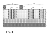
- FIG. 3 illustrates the formation of a mask 302 over portions of the insulator layer 220 .
- the mask 302 may be formed by, for example, a photolithographic process.
- the mask 302 may include, for example, an organic material.
- FIG. 4 illustrates a top view of the mask 302 arranged over portions of the insulator layer 220 .
- FIG. 5 illustrates a side view of the resultant structure following an etching process such as, for example, a reactive ion etching (RIE) process that removes exposed portions of the insulator layer 220 .
- the etching process is selective to the gate cap material on the gate stacks 210 and the spacers adjacent to the gate stacks 210 and results in cavities 502 and 504 adjacent to the gate stacks 210 a and 210 b respectively.
- the gate stack 210 cap layer and spacer materials may include, for example, a SiN or low k materials such as SiBCN, SiOCN, or SiOC.
- FIG. 6 illustrates the resultant structure after the mask 302 (of FIG. 5 ) is removed using a suitable process such as, for example an oxygen plasma ashing process.
- exposed portions of the liner layer 222 in the cavities 502 and 504 may be removed by a suitable etching process such as, for example a RIE process that is selective to the spacer materials.
- the exposed portions of the liner layer 222 may be removed after the insulator layer 220 is etched, but before the mask 302 is removed.
- the liner layer 222 may be removed when the mask 302 is removed or after the mask 302 is removed.
- FIG. 8 illustrates the resultant structure following a planarization process such as, for example, a chemical mechanical polishing (CMP) process that removes portions of the conductive material to define contacts 802 and 804 adjacent to the gates 210 a and 210 b .
- the contacts 802 of the FET devices 206 have a width w′ while the contacts 804 of the FET devices 208 have a width w′′.
- the width w′ is less than the width w′′.
- the gate stacks 210 a have a width G′ and the gate stacks 210 b have a width G′′ where the width G′ is less than the width G′′.
- the embodiments described herein provide devices with a reduced aspect ratio and contacts that reduce external resistance in the devices.
- the contacts remain arranged in the RX region (active region) of the device and do not extend beyond the edges of the RX region.
- the methods and structures described herein provide for contacts having different widths being formed using a single mask in a self-aligned patterning and etching process.
Landscapes
- Engineering & Computer Science (AREA)
- Power Engineering (AREA)
- Microelectronics & Electronic Packaging (AREA)
- Computer Hardware Design (AREA)
- Physics & Mathematics (AREA)
- Condensed Matter Physics & Semiconductors (AREA)
- General Physics & Mathematics (AREA)
- Manufacturing & Machinery (AREA)
- Ceramic Engineering (AREA)
- Electrodes Of Semiconductors (AREA)
- Thin Film Transistor (AREA)
- Metal-Oxide And Bipolar Metal-Oxide Semiconductor Integrated Circuits (AREA)
- Chemical & Material Sciences (AREA)
- Composite Materials (AREA)
- Materials Engineering (AREA)
Abstract
Description
Claims (6)
Priority Applications (2)
| Application Number | Priority Date | Filing Date | Title |
|---|---|---|---|
| US14/812,330 US9484264B1 (en) | 2015-07-29 | 2015-07-29 | Field effect transistor contacts |
| US14/963,601 US9761496B2 (en) | 2015-07-29 | 2015-12-09 | Field effect transistor contacts |
Applications Claiming Priority (1)
| Application Number | Priority Date | Filing Date | Title |
|---|---|---|---|
| US14/812,330 US9484264B1 (en) | 2015-07-29 | 2015-07-29 | Field effect transistor contacts |
Related Child Applications (1)
| Application Number | Title | Priority Date | Filing Date |
|---|---|---|---|
| US14/963,601 Continuation US9761496B2 (en) | 2015-07-29 | 2015-12-09 | Field effect transistor contacts |
Publications (1)
| Publication Number | Publication Date |
|---|---|
| US9484264B1 true US9484264B1 (en) | 2016-11-01 |
Family
ID=57189593
Family Applications (2)
| Application Number | Title | Priority Date | Filing Date |
|---|---|---|---|
| US14/812,330 Expired - Fee Related US9484264B1 (en) | 2015-07-29 | 2015-07-29 | Field effect transistor contacts |
| US14/963,601 Expired - Fee Related US9761496B2 (en) | 2015-07-29 | 2015-12-09 | Field effect transistor contacts |
Family Applications After (1)
| Application Number | Title | Priority Date | Filing Date |
|---|---|---|---|
| US14/963,601 Expired - Fee Related US9761496B2 (en) | 2015-07-29 | 2015-12-09 | Field effect transistor contacts |
Country Status (1)
| Country | Link |
|---|---|
| US (2) | US9484264B1 (en) |
Cited By (2)
| Publication number | Priority date | Publication date | Assignee | Title |
|---|---|---|---|---|
| US9761496B2 (en) * | 2015-07-29 | 2017-09-12 | International Business Machines Corporation | Field effect transistor contacts |
| US10186599B1 (en) * | 2017-07-20 | 2019-01-22 | International Business Machines Corporation | Forming self-aligned contact with spacer first |
Families Citing this family (5)
| Publication number | Priority date | Publication date | Assignee | Title |
|---|---|---|---|---|
| US10068980B1 (en) | 2017-04-26 | 2018-09-04 | International Business Machines Corporation | Vertical fin with a gate structure having a modified gate geometry |
| US11404423B2 (en) * | 2018-04-19 | 2022-08-02 | Taiwan Semiconductor Manufacturing Co., Ltd | Fin-based strap cell structure for improving memory performance |
| US10943990B2 (en) | 2018-10-25 | 2021-03-09 | International Business Machines Corporation | Gate contact over active enabled by alternative spacer scheme and claw-shaped cap |
| CN111370306B (en) * | 2018-12-26 | 2023-04-28 | 中芯集成电路(宁波)有限公司上海分公司 | Manufacturing method of transistor and full-surrounding grid electrode device structure |
| US10991689B2 (en) * | 2019-04-05 | 2021-04-27 | Globalfoundries U.S. Inc. | Additional spacer for self-aligned contact for only high voltage FinFETs |
Citations (29)
| Publication number | Priority date | Publication date | Assignee | Title |
|---|---|---|---|---|
| US6465310B2 (en) | 1998-11-20 | 2002-10-15 | Samsung Electronics Co., Ltd. | Methods of forming self-aligned contact pads on electrically conductive lines |
| US20070114612A1 (en) * | 2005-11-24 | 2007-05-24 | Samsung Electronics Co., Ltd. | Method of fabricating semiconductor devices having MCFET/finFET and related device |
| US20070141798A1 (en) | 2005-12-20 | 2007-06-21 | Intel Corporation | Silicide layers in contacts for high-k/metal gate transistors |
| US20070284669A1 (en) * | 2004-05-25 | 2007-12-13 | Abadeer Wagdi W | Method and structure to process thick and thin fins and variable fin to fin spacing |
| US20080093674A1 (en) * | 2004-12-03 | 2008-04-24 | Samsung Electronics Co., Ltd. | Fin field effect transistor and method of manufacturing the same |
| US7547947B2 (en) * | 2005-11-15 | 2009-06-16 | International Business Machines Corporation | SRAM cell |
| US8293616B2 (en) * | 2009-02-24 | 2012-10-23 | Taiwan Semiconductor Manufacturing Company, Ltd. | Methods of fabrication of semiconductor devices with low capacitance |
| US8298913B2 (en) * | 2010-10-12 | 2012-10-30 | International Business Machines Corporation | Devices with gate-to-gate isolation structures and methods of manufacture |
| US20120273895A1 (en) * | 2010-10-29 | 2012-11-01 | International Business Machines Corporation | Damascene method of forming a semiconductor structure and a semiconductor structure with multiple fin-shaped channel regions having different widths |
| US8440533B2 (en) | 2011-03-04 | 2013-05-14 | Globalfoundries Singapore Pte. Ltd. | Self-aligned contact for replacement metal gate and silicide last processes |
| US20130187171A1 (en) | 2012-01-23 | 2013-07-25 | Globalfoundries Inc. | Method to form silicide contact in trenches |
| US8604562B2 (en) * | 2010-06-21 | 2013-12-10 | Taiwan Semiconductor Manufacturing Company, Ltd. | Post CMP planarization by cluster ion beam etch |
| US8637359B2 (en) | 2011-06-10 | 2014-01-28 | International Business Machines Corporation | Fin-last replacement metal gate FinFET process |
| US8686514B2 (en) * | 2010-08-23 | 2014-04-01 | International Business Machines Corporation | Multiple threshold voltages in field effect transistor devices |
| US8815659B2 (en) * | 2012-12-17 | 2014-08-26 | Globalfoundries Inc. | Methods of forming a FinFET semiconductor device by performing an epitaxial growth process |
| US8878311B2 (en) | 2012-01-06 | 2014-11-04 | International Business Machines Corporation | Integrated circuit having raised source drains devices with reduced silicide contact resistance and methods to fabricate same |
| US8927378B2 (en) | 2010-11-11 | 2015-01-06 | International Business Machines Corporation | Trench silicide contact with low interface resistance |
| US8963257B2 (en) * | 2011-11-10 | 2015-02-24 | Taiwan Semiconductor Manufacturing Company, Ltd. | Fin field effect transistors and methods for fabricating the same |
| US8975712B2 (en) | 2013-05-14 | 2015-03-10 | Globalfoundries Inc. | Densely packed standard cells for integrated circuit products, and methods of making same |
| US8999779B2 (en) | 2013-09-06 | 2015-04-07 | International Business Machines Corporation | Locally raised epitaxy for improved contact by local silicon capping during trench silicide processings |
| US9029263B1 (en) * | 2013-12-12 | 2015-05-12 | Texas Instruments Incorporated | Method of printing multiple structure widths using spacer double patterning |
| US9041107B2 (en) * | 2010-10-12 | 2015-05-26 | International Business Machines Corporation | Devices with gate-to-gate isolation structures and methods of manufacture |
| US20150228722A1 (en) * | 2014-02-07 | 2015-08-13 | Samsung Electronics Co., Ltd. | Semiconductor device including fin-type field effect transistor |
| US20150294913A1 (en) * | 2013-05-06 | 2015-10-15 | International Business Machines Corporation | Method to make dual material finfet on same substrate |
| US9287129B2 (en) * | 2012-02-28 | 2016-03-15 | Taiwan Semiconductor Manufacturing Company, Ltd. | Method of fabricating FinFETs |
| US9299842B2 (en) * | 2012-09-14 | 2016-03-29 | Samsung Electronics Co., Ltd. | Fin transistor and semiconductor integrated circuit including the same |
| US20160093620A1 (en) * | 2013-07-15 | 2016-03-31 | Ju-youn Kim | Semiconductor device and method for fabricating the same |
| US20160104704A1 (en) * | 2014-10-08 | 2016-04-14 | Taiwan Semiconductor Manufacturing Co., Ltd | Semiconductor device structure and method for forming the same |
| US20160148998A1 (en) * | 2014-11-20 | 2016-05-26 | United Microelectronics Corporation | Finfet structure |
Family Cites Families (2)
| Publication number | Priority date | Publication date | Assignee | Title |
|---|---|---|---|---|
| US8896030B2 (en) * | 2012-09-07 | 2014-11-25 | Intel Corporation | Integrated circuits with selective gate electrode recess |
| US9484264B1 (en) * | 2015-07-29 | 2016-11-01 | International Business Machines Corporation | Field effect transistor contacts |
-
2015
- 2015-07-29 US US14/812,330 patent/US9484264B1/en not_active Expired - Fee Related
- 2015-12-09 US US14/963,601 patent/US9761496B2/en not_active Expired - Fee Related
Patent Citations (30)
| Publication number | Priority date | Publication date | Assignee | Title |
|---|---|---|---|---|
| US6465310B2 (en) | 1998-11-20 | 2002-10-15 | Samsung Electronics Co., Ltd. | Methods of forming self-aligned contact pads on electrically conductive lines |
| US20070284669A1 (en) * | 2004-05-25 | 2007-12-13 | Abadeer Wagdi W | Method and structure to process thick and thin fins and variable fin to fin spacing |
| US20080093674A1 (en) * | 2004-12-03 | 2008-04-24 | Samsung Electronics Co., Ltd. | Fin field effect transistor and method of manufacturing the same |
| US7547947B2 (en) * | 2005-11-15 | 2009-06-16 | International Business Machines Corporation | SRAM cell |
| US20070114612A1 (en) * | 2005-11-24 | 2007-05-24 | Samsung Electronics Co., Ltd. | Method of fabricating semiconductor devices having MCFET/finFET and related device |
| US20070141798A1 (en) | 2005-12-20 | 2007-06-21 | Intel Corporation | Silicide layers in contacts for high-k/metal gate transistors |
| US8293616B2 (en) * | 2009-02-24 | 2012-10-23 | Taiwan Semiconductor Manufacturing Company, Ltd. | Methods of fabrication of semiconductor devices with low capacitance |
| US8604562B2 (en) * | 2010-06-21 | 2013-12-10 | Taiwan Semiconductor Manufacturing Company, Ltd. | Post CMP planarization by cluster ion beam etch |
| US8686514B2 (en) * | 2010-08-23 | 2014-04-01 | International Business Machines Corporation | Multiple threshold voltages in field effect transistor devices |
| US9041107B2 (en) * | 2010-10-12 | 2015-05-26 | International Business Machines Corporation | Devices with gate-to-gate isolation structures and methods of manufacture |
| US8298913B2 (en) * | 2010-10-12 | 2012-10-30 | International Business Machines Corporation | Devices with gate-to-gate isolation structures and methods of manufacture |
| US20120273895A1 (en) * | 2010-10-29 | 2012-11-01 | International Business Machines Corporation | Damascene method of forming a semiconductor structure and a semiconductor structure with multiple fin-shaped channel regions having different widths |
| US8927378B2 (en) | 2010-11-11 | 2015-01-06 | International Business Machines Corporation | Trench silicide contact with low interface resistance |
| US8440533B2 (en) | 2011-03-04 | 2013-05-14 | Globalfoundries Singapore Pte. Ltd. | Self-aligned contact for replacement metal gate and silicide last processes |
| US8637359B2 (en) | 2011-06-10 | 2014-01-28 | International Business Machines Corporation | Fin-last replacement metal gate FinFET process |
| US8963257B2 (en) * | 2011-11-10 | 2015-02-24 | Taiwan Semiconductor Manufacturing Company, Ltd. | Fin field effect transistors and methods for fabricating the same |
| US8878311B2 (en) | 2012-01-06 | 2014-11-04 | International Business Machines Corporation | Integrated circuit having raised source drains devices with reduced silicide contact resistance and methods to fabricate same |
| US20130187171A1 (en) | 2012-01-23 | 2013-07-25 | Globalfoundries Inc. | Method to form silicide contact in trenches |
| US9287129B2 (en) * | 2012-02-28 | 2016-03-15 | Taiwan Semiconductor Manufacturing Company, Ltd. | Method of fabricating FinFETs |
| US9299842B2 (en) * | 2012-09-14 | 2016-03-29 | Samsung Electronics Co., Ltd. | Fin transistor and semiconductor integrated circuit including the same |
| US8815659B2 (en) * | 2012-12-17 | 2014-08-26 | Globalfoundries Inc. | Methods of forming a FinFET semiconductor device by performing an epitaxial growth process |
| US20150294913A1 (en) * | 2013-05-06 | 2015-10-15 | International Business Machines Corporation | Method to make dual material finfet on same substrate |
| US8975712B2 (en) | 2013-05-14 | 2015-03-10 | Globalfoundries Inc. | Densely packed standard cells for integrated circuit products, and methods of making same |
| US20160093620A1 (en) * | 2013-07-15 | 2016-03-31 | Ju-youn Kim | Semiconductor device and method for fabricating the same |
| US20160163706A1 (en) * | 2013-07-15 | 2016-06-09 | Ju-youn Kim | Semiconductor device and method for fabricating the same |
| US8999779B2 (en) | 2013-09-06 | 2015-04-07 | International Business Machines Corporation | Locally raised epitaxy for improved contact by local silicon capping during trench silicide processings |
| US9029263B1 (en) * | 2013-12-12 | 2015-05-12 | Texas Instruments Incorporated | Method of printing multiple structure widths using spacer double patterning |
| US20150228722A1 (en) * | 2014-02-07 | 2015-08-13 | Samsung Electronics Co., Ltd. | Semiconductor device including fin-type field effect transistor |
| US20160104704A1 (en) * | 2014-10-08 | 2016-04-14 | Taiwan Semiconductor Manufacturing Co., Ltd | Semiconductor device structure and method for forming the same |
| US20160148998A1 (en) * | 2014-11-20 | 2016-05-26 | United Microelectronics Corporation | Finfet structure |
Non-Patent Citations (1)
| Title |
|---|
| IBM; "Trench Silicide Contacts"; IP.com; IP.com No. 000184729; p. 1-2; Jul. 1, 2009. |
Cited By (2)
| Publication number | Priority date | Publication date | Assignee | Title |
|---|---|---|---|---|
| US9761496B2 (en) * | 2015-07-29 | 2017-09-12 | International Business Machines Corporation | Field effect transistor contacts |
| US10186599B1 (en) * | 2017-07-20 | 2019-01-22 | International Business Machines Corporation | Forming self-aligned contact with spacer first |
Also Published As
| Publication number | Publication date |
|---|---|
| US9761496B2 (en) | 2017-09-12 |
| US20170033016A1 (en) | 2017-02-02 |
Similar Documents
| Publication | Publication Date | Title |
|---|---|---|
| US9484264B1 (en) | Field effect transistor contacts | |
| US10770591B2 (en) | Source/drain contacts for non-planar transistors | |
| US9711647B2 (en) | Thin-sheet FinFET device | |
| US9257505B2 (en) | Structures and formation methods of finFET device | |
| US8492228B1 (en) | Field effect transistor devices having thick gate dielectric layers and thin gate dielectric layers | |
| US9196694B2 (en) | Integrated circuits with dual silicide contacts and methods for fabricating same | |
| KR101612646B1 (en) | Non-planar transistors and methods of fabrication thereof | |
| US10269644B2 (en) | Fin pitch scaling for high voltage devices and low voltage devices on the same wafer | |
| US10236253B2 (en) | Self-aligned local interconnect technology | |
| US20160260741A1 (en) | Semiconductor devices having fins, and methods of forming semiconductor devices having fins | |
| US9728622B1 (en) | Dummy gate formation using spacer pull down hardmask | |
| US10032680B2 (en) | Strained finFET device fabrication | |
| US20150024584A1 (en) | Methods for forming integrated circuits with reduced replacement metal gate height variability | |
| US9634010B2 (en) | Field effect transistor device spacers | |
| US8697514B2 (en) | FinFET device | |
| US10930768B2 (en) | Low current leakage finFET and methods of making the same | |
| CN114616654A (en) | Horizontal GAA nanowire and nano-flat transistor |
Legal Events
| Date | Code | Title | Description |
|---|---|---|---|
| AS | Assignment |
Owner name: INTERNATIONAL BUSINESS MACHINES CORPORATION, NEW Y Free format text: ASSIGNMENT OF ASSIGNORS INTEREST;ASSIGNORS:BASKER, VEERARAGHAVAN S.;CHENG, KANGGUO;STANDAERT, THEODORUS E.;AND OTHERS;SIGNING DATES FROM 20150717 TO 20150722;REEL/FRAME:036210/0098 |
|
| STCF | Information on status: patent grant |
Free format text: PATENTED CASE |
|
| AS | Assignment |
Owner name: ELPIS TECHNOLOGIES INC., CANADA Free format text: ASSIGNMENT OF ASSIGNORS INTEREST;ASSIGNOR:INTERNATIONAL BUSINESS MACHINES CORPORATION;REEL/FRAME:052620/0961 Effective date: 20200306 |
|
| FEPP | Fee payment procedure |
Free format text: MAINTENANCE FEE REMINDER MAILED (ORIGINAL EVENT CODE: REM.); ENTITY STATUS OF PATENT OWNER: LARGE ENTITY |
|
| LAPS | Lapse for failure to pay maintenance fees |
Free format text: PATENT EXPIRED FOR FAILURE TO PAY MAINTENANCE FEES (ORIGINAL EVENT CODE: EXP.); ENTITY STATUS OF PATENT OWNER: LARGE ENTITY |
|
| STCH | Information on status: patent discontinuation |
Free format text: PATENT EXPIRED DUE TO NONPAYMENT OF MAINTENANCE FEES UNDER 37 CFR 1.362 |
|
| FP | Expired due to failure to pay maintenance fee |
Effective date: 20201101 |