US9483663B2 - Countermeasure method for protecting stored data - Google Patents
Countermeasure method for protecting stored data Download PDFInfo
- Publication number
- US9483663B2 US9483663B2 US12/849,130 US84913010A US9483663B2 US 9483663 B2 US9483663 B2 US 9483663B2 US 84913010 A US84913010 A US 84913010A US 9483663 B2 US9483663 B2 US 9483663B2
- Authority
- US
- United States
- Prior art keywords
- data
- secret key
- list
- key
- cryptographic
- Prior art date
- Legal status (The legal status is an assumption and is not a legal conclusion. Google has not performed a legal analysis and makes no representation as to the accuracy of the status listed.)
- Active, expires
Links
Images


Classifications
-
- G—PHYSICS
- G06—COMPUTING; CALCULATING OR COUNTING
- G06F—ELECTRIC DIGITAL DATA PROCESSING
- G06F21/00—Security arrangements for protecting computers, components thereof, programs or data against unauthorised activity
- G06F21/70—Protecting specific internal or peripheral components, in which the protection of a component leads to protection of the entire computer
- G06F21/78—Protecting specific internal or peripheral components, in which the protection of a component leads to protection of the entire computer to assure secure storage of data
-
- G06F21/558—
-
- G—PHYSICS
- G06—COMPUTING; CALCULATING OR COUNTING
- G06F—ELECTRIC DIGITAL DATA PROCESSING
- G06F21/00—Security arrangements for protecting computers, components thereof, programs or data against unauthorised activity
- G06F21/60—Protecting data
- G06F21/62—Protecting access to data via a platform, e.g. using keys or access control rules
-
- G—PHYSICS
- G06—COMPUTING; CALCULATING OR COUNTING
- G06F—ELECTRIC DIGITAL DATA PROCESSING
- G06F21/00—Security arrangements for protecting computers, components thereof, programs or data against unauthorised activity
- G06F21/70—Protecting specific internal or peripheral components, in which the protection of a component leads to protection of the entire computer
- G06F21/71—Protecting specific internal or peripheral components, in which the protection of a component leads to protection of the entire computer to assure secure computing or processing of information
- G06F21/75—Protecting specific internal or peripheral components, in which the protection of a component leads to protection of the entire computer to assure secure computing or processing of information by inhibiting the analysis of circuitry or operation
- G06F21/755—Protecting specific internal or peripheral components, in which the protection of a component leads to protection of the entire computer to assure secure computing or processing of information by inhibiting the analysis of circuitry or operation with measures against power attack
-
- H—ELECTRICITY
- H04—ELECTRIC COMMUNICATION TECHNIQUE
- H04L—TRANSMISSION OF DIGITAL INFORMATION, e.g. TELEGRAPHIC COMMUNICATION
- H04L9/00—Cryptographic mechanisms or cryptographic arrangements for secret or secure communications; Network security protocols
- H04L9/002—Countermeasures against attacks on cryptographic mechanisms
- H04L9/003—Countermeasures against attacks on cryptographic mechanisms for power analysis, e.g. differential power analysis [DPA] or simple power analysis [SPA]
-
- H—ELECTRICITY
- H04—ELECTRIC COMMUNICATION TECHNIQUE
- H04L—TRANSMISSION OF DIGITAL INFORMATION, e.g. TELEGRAPHIC COMMUNICATION
- H04L9/00—Cryptographic mechanisms or cryptographic arrangements for secret or secure communications; Network security protocols
- H04L9/002—Countermeasures against attacks on cryptographic mechanisms
- H04L9/004—Countermeasures against attacks on cryptographic mechanisms for fault attacks
-
- H—ELECTRICITY
- H04—ELECTRIC COMMUNICATION TECHNIQUE
- H04L—TRANSMISSION OF DIGITAL INFORMATION, e.g. TELEGRAPHIC COMMUNICATION
- H04L9/00—Cryptographic mechanisms or cryptographic arrangements for secret or secure communications; Network security protocols
- H04L9/08—Key distribution or management, e.g. generation, sharing or updating, of cryptographic keys or passwords
- H04L9/0861—Generation of secret information including derivation or calculation of cryptographic keys or passwords
- H04L9/0869—Generation of secret information including derivation or calculation of cryptographic keys or passwords involving random numbers or seeds
-
- G—PHYSICS
- G06—COMPUTING; CALCULATING OR COUNTING
- G06F—ELECTRIC DIGITAL DATA PROCESSING
- G06F2221/00—Indexing scheme relating to security arrangements for protecting computers, components thereof, programs or data against unauthorised activity
- G06F2221/21—Indexing scheme relating to G06F21/00 and subgroups addressing additional information or applications relating to security arrangements for protecting computers, components thereof, programs or data against unauthorised activity
- G06F2221/2107—File encryption
-
- H—ELECTRICITY
- H04—ELECTRIC COMMUNICATION TECHNIQUE
- H04L—TRANSMISSION OF DIGITAL INFORMATION, e.g. TELEGRAPHIC COMMUNICATION
- H04L2209/00—Additional information or applications relating to cryptographic mechanisms or cryptographic arrangements for secret or secure communication H04L9/00
- H04L2209/12—Details relating to cryptographic hardware or logic circuitry
Definitions
- the present disclosure relates to a countermeasure method to protect stored sensitive data from attacks aiming to discover these data. It also relates to a portable microcircuit device implementing the method, such as a chip card.
- the sensitive data may notably be encryption or decryption keys, and more generally cryptographic data used or developed during cryptographic calculations, such as the intermediary data of such calculations, and identifiers kept secret. These data may be stored in a temporary or permanent manner in registers or memories, volatile such as memories of the RAM type, or non-volatile such as memories of the ROM and EEPROM types.
- Microcircuit devices storing such sensitive data are sometimes the object of attacks aiming to determine the data that they handle.
- attacks of the type SPA (Simple Power Analysis) or DPA (Differential Power Analysis) comprise measuring the currents and voltages going into and coming out of the microcircuit during the execution of a program by the microcircuit, with the aim of determining the protected data that the microcircuit treated or used.
- attacks of the type EMA (Electromagnetic Analysis) are based upon the analysis of electromagnetic radiation emitted by the microcircuit.
- Physical analysis type attacks target circuits such as the memories and registers, of the ROM type, with the aim of determining the data stored during the fabrication of the circuit, or the cryptographic calculation circuits in order to determine the calculations performed.
- fault injection attacks consist of introducing disruptions into the microcircuit while it is executing sensitive algorithms such as cryptographic algorithms, or with the aim of launching an uploading routine that emits, upon one of the ports, data that is memorized.
- a disruption may be caused by applying to the microcircuit, on one of its contacts, one or more brief lightings or voltage peaks.
- the disclosure relates in particular to those which aim to protect the data stored by a microcircuit, whether they are stored permanently or temporarily.
- Embodiments of the present disclosure relate to a method of read or write access by an electronic component to storage addresses of data, comprising steps of applying a cryptographic operation using a secret key for each data read or to be written, generating a first secret key for a first data of an ordered list of data read or to be written, and for each data of the list, following the first data, generating a distinct secret key by means of a deterministic function applied to a secret key generated for a previous data of the list, the application of the cryptographic operation to each data read or to be written of the list carried out by using the secret key generated for the data.
- the deterministic function is a generation function of pseudo-random numbers.
- a secret key is generated by applying the deterministic function to a secret key generated for a previous data of the list, and to the data read or to be written, before or after the application of the cryptographic operation to the previous data.
- the method comprises steps of comparison of a last data accessed of the list and treated by the cryptographic operation to a reference data, and if the comparison reveals a difference, the electronic component passes into an error state.
- the generation of a secret key for a data of the list is started by a particular instruction detected before the access to the data, during the execution of a program by the electronic component.
- the generation of a secret key for a data of the list is started when the address of the data belongs to an ensemble of particular addresses.
- the cryptographic operation applied to the accessed data uses a common secret key.
- the first secret key is generated by applying the deterministic function to an initial value.
- the method comprises two consecutive read accesses to a same storage address of data, carried out by using two distinct secret keys so that the cryptographic operation supplies two different data.
- the method comprises two consecutive read accesses to two distinct data storage addresses, carried out by using two distinct secret keys such that the cryptographic operation supplies two identical data.
- Embodiments of the present disclosure also relate to an electronic component configured to implement the method according to one of the above embodiments.
- the electronic component comprises a processor configured to implement the method according to one of the above embodiments.
- the electronic component comprises a processor, memories connected to the processor by a bus, and a countermeasure device interposed between each memory and the bus and configured to implement the method according to one of the embodiments disclosed herein.
- Embodiments of the present disclosure also relate to a microcircuit portable device comprising an electronic component according to one of the above embodiments.
- a method of read or write access by an electronic component to storage addresses of data comprises a step of applying a cryptographic operation using a secret key for each data read or to be written, comprising steps of: generating a first secret key for a first data of an ordered list of data read or to be written, and for each data of the list, following the first data, generating a distinct secret key by means of a deterministic function applied to a secret key generated for a previous data of the list, the application of the cryptographic operation to each data read or to be written of the list carried out by using the secret key generated for the data.
- the deterministic function is a generation function of pseudo-random numbers.
- a secret key is generated by applying the deterministic function to a secret key generated for a previous data of the list, and to the data read or to be written, before or after the application of the cryptographic operation to the previous data.
- the method comprises steps of comparison of a last data accessed of the list and treated by the cryptographic operation to a reference data, and if the comparison reveals a difference, the electronic component passes into an error state.
- the generation of a secret key for a data of the list is started by a particular instruction detected before the access to the data, during the execution of a program by the electronic component.
- the generation of a secret key for a data of the list is started when the address of the data belongs to an ensemble of particular addresses.
- the cryptographic operation applied to the accessed data uses a common secret key.
- the first secret key is generated by applying the deterministic function to an initial value.
- the method comprises two consecutive read accesses to a same storage address of data, carried out by using two distinct secret keys so that the cryptographic operation supplies two different data.
- the method comprising two consecutive read accesses to two distinct data storage addresses, carried out by using two distinct secret keys such that the cryptographic operation supplies two identical data.
- a method comprises: generating a first secret key for a first data of an ordered list of data read or to be written by an electronic device; for each data of the list, following the first data, generating a distinct secret key based on a deterministic function; applying a cryptographic operation to each data read or to be written of the list based on the secret key generated for the data, wherein the deterministic function is applied to a secret key generated for a previous data of the list and at least one of: the previous data; and a result of application of the cryptographic operation to the previous data; comparing a result of application of the cryptographic operation to a last data of the ordered list to a reference data; and selectively causing the electronic device to enter an error state based on the comparison.
- the deterministic function is a generation function of pseudo-random numbers.
- the electronic device passes into the error state.
- the generation of a secret key for a data of the list is started by a particular instruction detected before the access to the data, during the execution of a program by the electronic device.
- the generation of a secret key for a data of the list is started when an address of the data belongs to an ensemble of particular addresses.
- the cryptographic operation applied to the accessed data uses a common secret key.
- the first secret key is generated by applying the deterministic function to an initial value.
- the method comprises performing two consecutive read accesses to a same storage address of data, carried out by using two distinct secret keys so that the cryptographic operation supplies two different data. In an embodiment, the method comprises performing two consecutive read accesses to two distinct data storage addresses, carried out by using two distinct secret keys such that the cryptographic operation supplies two identical data.
- an electronic device comprises: a key generator configured to: generate a first secret key for a first data of an ordered list of data read or to be written by the electronic device; and for each data of the list, following the first data, generate a distinct secret key based on a deterministic function; a cryptographic unit coupled to the key generator and configured to apply a cryptographic operation to each data read or to be written of the list based on the secret key generated for the data, wherein the deterministic function is applied to a secret key generated for a previous data of the list and at least one of: the previous data; and a result of application of the cryptographic operation to the previous data; and a comparator configured to: compare a result of application of the cryptographic operation to a last data of the ordered list to a reference data; and control a state of the electronic device based on the comparison.
- the deterministic function is a generation function of pseudo-random numbers.
- the comparator is configured to generate a signal to cause the electronic device to enter an error state when the comparison reveals a difference.
- the electronic device further comprises a processor configured to execute instructions, wherein the generation of a secret key for a data of the list is started by a particular instruction detected before the access to the data, during the execution of a program by the electronic device.
- the electronic device further comprises an address decoder, wherein the key generator is configured to start generation of a secret key for a data of the list when the address decoder determines an address of the data belongs to an ensemble of particular addresses.
- the key generator is configured to generate the first secret key by applying the deterministic function to an initial value.
- the cryptographic unit is configured to perform two consecutive cryptographic operations on data associated with a single storage address, carried out by using two distinct secret keys, producing two different output data.
- the cryptographic unit is configured to perform two consecutive cryptographic operations on data associated with two distinct data storage addresses, carried out by using two distinct secret keys, producing identical output data.
- a system comprises: a processor; a memory; a countermeasure device coupled between the processor and the memory, the countermeasure device comprising: a key generator configured to: generate a first secret key for a first data of an ordered list of data to be transferred between the processor and the memory; and for each data of the list, following the first data, generate a distinct secret key based on a deterministic function; and a cryptographic unit coupled to the key generator and configured to apply a cryptographic operation to each data of the list based on the secret key generated for the data, wherein the deterministic function is applied to a secret key generated for a previous data of the list and at least one of: the previous data; and a result of application of the cryptographic operation to the previous data; and an error detector configured to: compare a result of application of the cryptographic operation to a last data of the ordered list to a reference data; and control a state of the system based on the comparison.
- a key generator configured to: generate a first secret key for a first data of an ordered list of
- the error detector is configured to generate a signal to cause the electronic device to enter an error state when the comparison reveals a difference.
- the generation of a secret key for a data of the list is started by a particular instruction detected before the access to the data, during the execution of a program by the processor.
- the system further comprises an address decoder, wherein the key generator is configured to start generation of a secret key for a data of the list when the address decoder determines an address of the data belongs to an ensemble of particular addresses.
- the cryptographic unit is configured to perform two consecutive cryptographic operations on data associated with a single storage address, carried out by using two distinct secret keys, producing two different output data.
- the cryptographic unit is configured to perform two consecutive cryptographic operations on data associated with two distinct data storage addresses, carried out by using two distinct secret keys, producing identical output data.
- a device comprises: means for generating a first secret key for a first data of an ordered list of data, and, for each data of the list following the first data, generating a distinct secret key based on a deterministic function; means for applying a cryptographic operation to each data read or to be written of the list based on the secret key generated for the data, wherein the deterministic function is applied to a secret key generated for a previous data of the list and at least one of: the previous data; and a result of application of the cryptographic operation to the previous data; and means for causing the device to enter an error state when a result of application of the cryptographic operation to a last data of the ordered list differs from a reference data.
- the device further comprises: means for activating the means for generating. In an embodiment, the device further comprises: means for supplying the means for applying a cryptographic operation with a fixed key or a key generated by the means for generating. In an embodiment, the device further comprises: means for selecting between an output and an input of the means for applying a cryptographic operation.
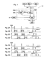
- FIG. 1 shows schematically a countermeasure device to protect data stored in an electronic component, according to one embodiment
- FIGS. 2A to 2D are timing diagrams showing steps of a read access of protected data in the electronic component, according to one embodiment
- FIGS. 3A to 3D are timing diagrams showing steps of a write access of protected data in the electronic component, according to one embodiment
- FIG. 4 shows schematically a countermeasure device to protect data stored in an electronic component, according to another embodiment
- FIG. 5 shows an electronic component equipped with a countermeasure device, according to one embodiment
- FIG. 6 shows an electronic component equipped with a countermeasure device, according to another embodiment
- FIG. 7 is a chart showing steps of a read access of stored data, according to one embodiment.
- FIG. 8 is a chart showing steps of a write access of stored data, according to one embodiment.
- FIG. 9 shows schematically two memories of the electronic component, protected by an embodiment of a countermeasure device.
- FIG. 1 shows a data path DPT in an embodiment of an electronic component 100 , between data sources SRC 1 , SRC 2 , . . . SRCn and a destination DEST.
- a countermeasure device PRD to protect the data stored in the electronic component is interposed on the path DPT.
- the sources SRC 1 -SRCn and the destination DEST are for example addresses in a memory and/or registers, belonging to the component itself or external to the component.
- the device PRD comprises a cryptographic calculation unit ECDC interposed on the data path DPT between the data sources SRC 1 -SRCn and the destination DEST.
- the unit ECDC applies a cryptographic operation to a data ED ⁇ i> received and supplies a transformed data D ⁇ i>.
- the cryptographic operation may be an encryption or decryption operation, for example of a symmetric type.
- the device PRD may also comprise a multiplexer MUX 1 comprising an input connected to a data output of the unit ECDC, one input connected to data sources SRC 1 -SRCn and one output connected to the destination DEST.
- the multiplexer MUX 1 is controlled by an address decoder ADEC receiving on input a source or destination address AD of a data ED ⁇ i> transferred in the path DPT.
- the multiplexer MUX 1 thus optionally allows to encrypt/decrypt or to let a data ED ⁇ i> circulate in the path DPT without being encrypted/decrypted, depending on the address of the source or of the destination of the data, or both.
- the countermeasure device PRD also comprises a key generation unit KGEN supplying secret keys SK ⁇ i> to a key input of the unit ECDC.
- the unit ECDC is configured to encrypt or decrypt each data ED ⁇ i> received with the last key SK ⁇ i> received from the unit KGEN.
- the unit KGEN receives a synchronization signal that starts the supply of a key SK ⁇ i> to the unit ECDC.
- the deterministic function PRF employed by the unit KGEN to generate the keys SK ⁇ i> may be a pseudo-random number generation function. Such a function may combine logic operations such as shifts, addition and/or multiplication. It may for example be performed by means of a Linear Feedback Shift Register (LFSR). It may also be performed by means of a substitution table SBOX such as those used in symmetric encryption algorithms, the substitution table being looped back upon itself such that the next state of the table depends upon its previous state.
- the signal SYNC may be emitted by the address decoder ADEC when an address or a specific zone of addresses is accessed. It may also be emitted, during the reading of a particular instruction code, by a processor of the electronic component executing a program.
- the protected data ED ⁇ i> are accessed in a deterministic order, generally defined by the program executed by the electronic component. It suffices therefore to encrypt and store in the electronic component the protected data in the order in which they will be read by the electronic component, by using the keys obtained by the deterministic function implemented by the unit KGEN, from a same initial value also stored in the electronic component.
- the unit ECDC may be made by simple logic gates exclusive OR (XOR), each combining a bit of a data to encrypt or to decrypt ED ⁇ i> with a respective bit of a key SK ⁇ i>.
- FIGS. 2A, 2B, 2C and 2D are respective timing diagrams of the signal SYNC, of a signal supplied to a key input of the unit ECDC, of a signal supplied to a data input of the unit ECDC, and of a signal of data output from the unit ECDC, for example in the case of an encrypted data read.
- the signal SYNC comprises pulses that are emitted by the component at instants when a data is to be decrypted by the unit ECDC.
- the unit KGEN At each pulse of signal SYNC, the unit KGEN generates a key SK 1 , SK 2 , . . . SK ⁇ n> that it transmits to the unit ECDC ( FIG. 2B ).
- the unit ECDC receives a data to decrypt ED 1 , ED 2 , . . . ED ⁇ n> ( FIG. 2C ) and decrypts it by using the last key received. Therefore, the unit ECDC supplies decrypted data D 1 , D 2 , . . . DSK ⁇ n> ( FIG. 2D ) corresponding to the encrypted data ED 1 , ED 2 , . . . ED ⁇ n> received.
- FIGS. 3A, 3B, 3C and 3D are timing diagrams respectively of the signal SYNC, of the signal supplied to a key input of the unit ECDC, of the signal supplied to a data input of the unit ECDC, and of the signal of data output from the unit ECDC, for example in the case of a data write.
- the unit KGEN At each pulse of signal SYNC shown in FIG. 3A , the unit KGEN generates a key SK 1 , SK 2 , . . . SK ⁇ n> that it transmits to the unit ECDC ( FIG. 3B ).
- the unit ECDC receives a data to encrypt D 1 , D 2 , . . . D ⁇ n> ( FIG.
- the unit ECDC supplies encrypted data ED 1 , ED 2 , . . . ED ⁇ n> ( FIG. 3D ) corresponding to un-encrypted data D 1 , D 2 , . . . D ⁇ n> received.
- the order in which these data will be read is defined by the program executed by the electronic component. This order, which defines an ordered list of accessed addresses, is respected to define with which secret key SK ⁇ i>, generated by the unit KGEN, each data to be written is encrypted before it is written in the memory.
- the unit KGEN is first initialized with the same initial value as that used for the encryption of the stored data. At each address read of a stored data, the unit KGEN supplies a new secret key to be used to decrypt the data read.
- the unit KGEN may be initialized with a randomly generated initial value. Then, each sensitive data to be written in the memory is encrypted beforehand by means of a new secret key generated by the unit KGEN. To access sensitive data thus stored in the volatile memory, the unit KGEN is first initialized with the initial value used during the writing of the sensitive data in the volatile memory. The sensitive data are then read and decrypted in the order in which they were stored in the memory, by using a new secret key generated by the unit KGEN at each read of a sensitive data. The initial value used by the unit KGEN is therefore different for each session of the electronic component, or for each write access in the volatile memory.
- a fraudulent access of protected data requires the determination of the non-volatile memory zone where the initial value IVAL is stored and the analysis of this memory zone, the analysis of the key generation unit KGEN to determine the deterministic function used, the analysis of the unit ECDC to determine the encryption algorithm implemented, the localization of the memory zones where the protected data are stored and the analysis of these zones in order to extract the encrypted data. If a data uploading operation from a memory is fraudulently launched, it seems that it would be difficult to initialize at the same time the unit KGEN with the correct initial value and to correctly synchronize it in order to decrypt the uploaded data.
- the countermeasure device PRD may be made on a relatively small integrated circuit area, and may only impose during the writing of the program executed by the electronic component so as to determine the access order of the protected data, and to control the initialization of the unit KGEN with the initial value used during the writing of the protected data.
- the unit KGEN may be initialized several times with different values. It may also be provided to not use all the keys generated by the unit KGEN by sending several synchronization pulses to it without activating the unit ECDC to encrypt or decrypt a data.
- the data is known ahead of time. In this manner, it is possible to verify that no data of an ordered list of data read was fraudulently modified by comparing a last data of the list, read and treated by the unit ECDC, with a reference value.
- DFA Different Fault Analysis
- FIG. 4 shows a countermeasure device PRD 1 according to another embodiment.
- the device PRD 1 differs from device PRD shown in FIG. 1 in that it comprises a second multiplexer MUX 2 interposed between the key generation unit KGEN and the cryptographic calculation unit ECDC.
- the multiplexer MUX 2 sends to the unit ECDC either a key SK ⁇ i> supplied by the unit KGEN, or else a fixed key SSK provided to encrypt less sensitive data, as a function of the address AD of the data read or to store.
- the multiplexer MUX 2 is controlled by a signal from the address decoder ADEC.
- FIG. 4 also shows an error detector ERRO comprising a comparator COMP configured to compare an output of the cryptographic calculation unit ECDC of a last data in a list of data to reference data REFD, and to generate an output signal ER based on the comparison.
- the signal ER when the comparison indicates a difference, causes the device or a system including the device to enter an error state.
- FIG. 5 shows an electronic component IC comprising a processor MP, for example of the microprocessor or microcontroller type, memories MEM 1 , MEM 2 , MEM 3 , an interface unit INT allowing the component to communicate with external equipment, and address and data buses ADB to which the processor, the memories, and the interface unit are connected.
- the memories MEM 1 , MEM 2 are for example non-volatile memories and the memory MEM 3 a volatile memory for example of the type RAM.
- the memories MEM 1 and MEM 2 are for example of the type ROM and EEPROM.
- the component IC may also comprise cryptographic calculation circuits CAU also connected to the buses ADB.
- the electronic component IC comprises countermeasure devices PRD 1 , PRD 2 , PRD 3 such as those previously described in reference to FIG. 1 or 4 , interposed between each of the memories MEM 1 , MEM 2 , MEM 3 and the address bus ADB.
- each of devices PRD 1 , PRD 2 , PRD 3 comprises its own key generation unit KGEN.
- one unit KGEN may be shared by two or more of the countermeasure devices PRD 1 , PRD 2 , PRD 3 , to supply a secret key to the cryptographic calculation units ECDC of each of the countermeasure devices, as a sensitive data is accessed in one or another of the memories MEM 1 , MEM 2 , MEM 3 .
- FIG. 6 shows an electronic component 101 according to another embodiment.
- the component 101 only differs from component IC in that it comprises only one countermeasure device PRD interposed between the processor MP and the bus ADB.
- the sensitive data read in the memories are transmitted by the data bus in an encrypted form and are decrypted just before being used by the processor MP.
- the sensitive data supplied by the processor MP are encrypted before being transmitted by the data bus to be stored in an encrypted form in a memory or a register.
- FIGS. 7 and 8 show sequences of steps of a countermeasure method according to one embodiment.
- FIG. 7 shows a read sequence P 1 of a data stored at an address AD.
- the sequence P 1 comprises steps S 1 to S 7 .
- the processor MP reads a data ED at the address AD.
- the processor executes steps S 3 and S 4 , otherwise it executes step S 5 .
- the processor orders the generation of a new key SK 1 , as a function of a previous key SK 0 , and the new key SK 1 is stored as the previous key SK 0 .
- the key SK 1 is the first key of an ordered list of generated keys
- the key SK 0 is initialized with an initial value IVAL before the sequence P 1 is executed.
- the initial value IVAL is that which was used to initialize the sequence of keys used during the writing of the data to be read.
- the processor orders the decryption of the data ED, by means of the key SK 1 , to obtain a decrypted data D.
- step S 5 if the read address belongs to addresses of less sensitive yet still encrypted data, the processor executes step S 6 , otherwise it executes step S 7 .
- step S 6 the processor MP decrypts the data ED to obtain a decrypted data D, by using a key SSK used to encrypt all or part of the less sensitive yet still encrypted data.
- step S 7 the data ED read in the memory correspond to the data decrypted D.
- the sequence P 1 of steps finishes at the end of step S 4 , S 6 or S 7 by the supply of non-encrypted data D.
- FIG. 8 shows a write sequence P 2 of a data D at an address AD.
- the sequence P 2 comprises steps S 11 to S 17 .
- the processor MP determines whether the write address corresponds to a storage address of a sensitive data. If so, then the processor executes the steps S 12 to S 14 , otherwise it executes the step S 15 .
- the processor orders the generation of a new key SK 1 to be used to encrypt the data D as a function of a previous key SK 0 , and the new key SK 1 is stored as the previous key SK 0 .
- the key SK 1 is the first key of an ordered list of generated keys
- the key SK 0 is initialized at an initial value IVAL before the execution of the sequence P 2 .
- the processor encrypts the data D by means of the key SK 1 to obtain an encrypted data ED.
- the processor MP writes the encrypted data ED at the address AD.
- the processor executes step S 16 , otherwise it executes step S 17 .
- the processor MP encrypts the data D to obtain an encrypted data ED, by using the key SSK used to encrypt all or part of the less sensitive yet still encrypted data.
- step S 17 the data D to store correspond to the data ED to be written at address AD.
- the processor MP executes step S 14 to write the data ED at the address AD.
- the sequence P 2 of steps finishes at the end of step S 14 .
- the calculation of a new key may be completely done by the processor or by an external circuit, for example by the circuit CAU.
- the decryption and encryption operations performed at steps S 4 , S 6 , S 13 and S 16 may be done by the processor MP or by an external circuit, such as the circuit CAU.
- the emission of the signal SYNC may be not necessary.
- the processor MP itself may order a new key SK 1 each time a sensitive data is to be encrypted or decrypted.
- the steps S 3 and S 12 may also be replaced by the emission of the synchronization signal SYNC to start the generation of a new key.
- FIG. 9 shows the memories MEM 1 , MEM 2 of the electronic component of FIG. 6 , protected by countermeasure devices PRD 1 , PRD 2 , such as that shown in FIG. 4 .
- the device PRD 1 comprises a cryptographic calculation unit ECDC 1 , multiplexers MUX 1 , MUX 2 , and a key generation unit KGN 1 .
- the unit ECDC 1 is connected to a data output of the memory MEM 1 .
- the multiplexer MUX 1 comprises an input connected to a data output of the unit ECDC 1 , an input connected to a data output of the memory MEM 1 , and a data D output.
- the multiplexer MUX 2 sends to the unit ECDC 1 either a key supplied by the unit KGN 1 , or else a fixed key SSK 1 common to several protected data.
- the unit KGN 1 is initialized by an initial value IVAL 1 stored in the memory MEM 2 .
- the device PRD 2 comprises a cryptographic calculation unit ECDC 2 , multiplexers MUX 3 , MUX 4 , and a key generation unit KGN 2 .
- the unit ECDC 2 is connected to a data output of the memory MEM 2 .
- the multiplexer MUX 3 comprises an input connected to a data output of the unit ECDC 2 , an input connected to the data output of the memory MEM 2 , and a data D output.
- the multiplexer MUX 4 sends to the unit ECDC 2 either a key supplied by the unit KGN 2 , or else a fixed key SSK 2 common to several protected data.
- the unit KGN 2 is initialized by an initial value IVAL 2 stored in the memory MEM 1 .
- the units KGN 1 , KGN 2 are synchronized by signals SYNC 1 , SYNC 2 , which may be identical or different.
- the initial value IVAL 1 stored in the memory MEM 2 . It is also necessary to know the encryption algorithm implemented by the unit ECDC 1 and the algorithm implemented by the unit KGN 1 . If the initial value IVAL 1 is encrypted by means of an encryption key generated by the unit KGN 2 , it is also necessary to know the encryption algorithm implemented by the unit ECDC 2 and the algorithm implemented by the unit KGN 2 , as well as the initial value IVAL 2 used by the unit KGN 2 . The initial value IVAL 2 may be stored in the memory MEM 1 in an encrypted form by means of the key SSK 1 . It is therefore necessary to also know this key. In other words, the access to a sensitive data requires the knowledge of a large number of the circuits of the electronic component as well as the stored data.
- Certain cryptographic calculations such as 3-DES (Data Encryption Standard), use two cryptographic keys.
- An embodiment of a device according to the disclosure allows for the reading of two different keys at the same addresses of the memory, by using different decryption keys SK supplied by the unit KGEN, that is to say generated from different previous values.
- the two cryptographic keys may be obtained by reading two times the address or the same addresses and by starting the generation of a new decryption key for each read.
- the electronic component may read two different data at the same storage address.
- the electronic component IC, IC 1 emits identical electromagnetic signatures and electrical consumption signatures during the reading of two cryptographic keys.
- a countermeasure device may also allow the storage of a same cryptographic key at two different addresses in the form of two different values resulting from an encryption using two different keys generated by the unit KGEN from different previous values. In this manner, a cryptographic key may be accessed several times at different addresses, while the electronic component emits different electromagnetic and electrical consumption signatures.
- the disclosure is not limited to a deterministic function supplying a new secret key as a function of a previously generated secret key, and if necessary, of a data previously encrypted or decrypted.
- the deterministic function may also relate to, for example, a second previously generated secret key and/or any other determinable value, such as an order number in the ordered list of secret keys generated, or the address of the last data accessed or of the previous data accessed.
- the access method previously described does not require that the accessed addresses be consecutive or accessed in an increasing or deceasing order of their respective values, or that the data be accessed in a certain order. It only matters that the order in which the data were written at these addresses is determinable and that this order is taken into consideration during the read access of these addresses, so that the secret key used to decrypt a data read is that which was used to encrypt the data. It also is not necessary to read all the data written during a write sequence. Indeed, if a data does not need to be read, it suffices to request two times the generation of a key by the unit KGEN to be able to access the following data in the sequence.
- the data protected by a key generated by the unit KGEN may be read in any order, as long as the order in which these data were written is known, that is to say the rank of their encryption key in the ordered list of generated keys.
- each data may be read and decrypted by ordering the initialization of the unit KGEN with the initial value IVAL and by ordering the generation of a key a number of times corresponding to the rank in the list of generated keys of the encryption key of the data.
- Each data may be equally read and decrypted by means of a key obtained by initializing the unit KGEN with the value of the key SK ⁇ n> having a rank n in the list of generated keys, immediately less than that n+1 of the key SK ⁇ n+1> to be used to decrypt the data to be read, by application of the formula (2).
- the cryptographic operation performed by the cryptographic calculation unit ECDC is not necessarily an encryption or decryption operation. Indeed, this operation may also perform a signature calculation.
- the unit ECDC may apply the same cryptographic function to encrypt and to decrypt a data or apply different functions.
- a computer readable medium comprising a computer program adapted to perform one or more of the methods described above.
- the medium may be a physical storage medium such as for example a Read Only Memory (ROM) chip, or a disk such as a Digital Versatile Disk (DVD-ROM), Compact Disk (CD-ROM), a hard disk, a memory, a network, or a portable media article to be read by an appropriate drive or via an appropriate connection, including as encoded in one or more barcodes or other related codes stored on one or more such computer-readable mediums and being readable by an appropriate reader device.
- ROM Read Only Memory
- DVD-ROM Digital Versatile Disk
- CD-ROM Compact Disk
- some or all of the systems and/or modules may be implemented or provided in other manners, such as at least partially in firmware and/or hardware, including, but not limited to, one or more application-specific integrated circuits (ASICs), discrete circuitry, standard integrated circuits, controllers (e.g., by executing appropriate instructions, and including microcontrollers and/or embedded controllers), field-programmable gate arrays (FPGAs), complex programmable logic devices (CPLDs), etc., as well as devices that employ RFID technology.
- ASICs application-specific integrated circuits
- controllers e.g., by executing appropriate instructions, and including microcontrollers and/or embedded controllers
- FPGAs field-programmable gate arrays
- CPLDs complex programmable logic devices
- some of the modules or controllers separately described herein may be combined, split into further modules and/or split and recombined in various manners.
- the systems, modules and data structures may also be transmitted as generated data signals (e.g., as part of a carrier wave) on a variety of computer-readable transmission mediums, including wireless-based and wired/cable-based mediums.
Landscapes
- Engineering & Computer Science (AREA)
- Computer Security & Cryptography (AREA)
- Theoretical Computer Science (AREA)
- Computer Hardware Design (AREA)
- Physics & Mathematics (AREA)
- Signal Processing (AREA)
- Computer Networks & Wireless Communication (AREA)
- Software Systems (AREA)
- General Engineering & Computer Science (AREA)
- General Physics & Mathematics (AREA)
- Health & Medical Sciences (AREA)
- General Health & Medical Sciences (AREA)
- Bioethics (AREA)
- Mathematical Physics (AREA)
- Storage Device Security (AREA)
Applications Claiming Priority (2)
| Application Number | Priority Date | Filing Date | Title |
|---|---|---|---|
| FR0903865 | 2009-08-05 | ||
| FR0903865A FR2949010A1 (fr) | 2009-08-05 | 2009-08-05 | Procede de contremesure pour proteger des donnees memorisees |
Publications (2)
| Publication Number | Publication Date |
|---|---|
| US20110033045A1 US20110033045A1 (en) | 2011-02-10 |
| US9483663B2 true US9483663B2 (en) | 2016-11-01 |
Family
ID=41581149
Family Applications (1)
| Application Number | Title | Priority Date | Filing Date |
|---|---|---|---|
| US12/849,130 Active 2031-06-26 US9483663B2 (en) | 2009-08-05 | 2010-08-03 | Countermeasure method for protecting stored data |
Country Status (3)
| Country | Link |
|---|---|
| US (1) | US9483663B2 (fr) |
| EP (1) | EP2284748B1 (fr) |
| FR (1) | FR2949010A1 (fr) |
Families Citing this family (5)
| Publication number | Priority date | Publication date | Assignee | Title |
|---|---|---|---|---|
| DE102012209404A1 (de) * | 2012-06-04 | 2013-12-05 | Robert Bosch Gmbh | Vorrichtung zur Ausführung eines kryptographischen Verfahrens und Betriebsverfahren hierfür |
| EP3084968A4 (fr) * | 2013-12-16 | 2017-11-29 | McAfee, LLC | Prétraitement efficace de processus pour un standard de chiffrement |
| US10984136B2 (en) * | 2017-04-21 | 2021-04-20 | Micron Technology, Inc. | Secure memory device with unique identifier for authentication |
| CN108199832B (zh) * | 2017-12-28 | 2021-02-26 | 东华大学 | 一种cloc认证加密算法抵御差分故障攻击的检测方法 |
| CN111464568B (zh) * | 2020-06-17 | 2020-09-25 | 广东电网有限责任公司佛山供电局 | 一种增强多网口防网络攻击能力的方法和系统 |
Citations (10)
| Publication number | Priority date | Publication date | Assignee | Title |
|---|---|---|---|---|
| US5146498A (en) * | 1991-01-10 | 1992-09-08 | Motorola, Inc. | Remote key manipulations for over-the-air re-keying |
| WO2003085881A1 (fr) | 2002-04-08 | 2003-10-16 | Oberthur Card Systems S.A. | Procede de securisation d'une entite electronique a acces crypte |
| US20040179690A1 (en) * | 2003-03-13 | 2004-09-16 | New Mexico Technical Research Foundation | Dynamic security authentication for wireless communication networks |
| US20050114653A1 (en) * | 1999-07-15 | 2005-05-26 | Sudia Frank W. | Certificate revocation notification systems |
| US6996723B1 (en) * | 1999-08-10 | 2006-02-07 | Fuji Xerox Co., Ltd. | Data generating apparatus and data verifying apparatus |
| US7110539B1 (en) | 1999-03-22 | 2006-09-19 | Kent Ridge Digital Labs | Method and apparatus for encrypting and decrypting data |
| US20060212506A1 (en) * | 2005-03-19 | 2006-09-21 | Samsung Electronics Co., Ltd. | Scalar multiplication apparatus and method |
| WO2007069236A2 (fr) | 2005-12-14 | 2007-06-21 | Nds Limited | Procede et systeme pour l'usage de criptage de chiffrement par bloc |
| JP2007195132A (ja) | 2005-12-20 | 2007-08-02 | Sony Corp | 暗号処理装置 |
| US20090028143A1 (en) * | 2007-07-26 | 2009-01-29 | Anand Eswaran | Pattern Matching In A Network Flow Across Multiple Packets |
-
2009
- 2009-08-05 FR FR0903865A patent/FR2949010A1/fr not_active Withdrawn
-
2010
- 2010-07-29 EP EP10007904.5A patent/EP2284748B1/fr active Active
- 2010-08-03 US US12/849,130 patent/US9483663B2/en active Active
Patent Citations (10)
| Publication number | Priority date | Publication date | Assignee | Title |
|---|---|---|---|---|
| US5146498A (en) * | 1991-01-10 | 1992-09-08 | Motorola, Inc. | Remote key manipulations for over-the-air re-keying |
| US7110539B1 (en) | 1999-03-22 | 2006-09-19 | Kent Ridge Digital Labs | Method and apparatus for encrypting and decrypting data |
| US20050114653A1 (en) * | 1999-07-15 | 2005-05-26 | Sudia Frank W. | Certificate revocation notification systems |
| US6996723B1 (en) * | 1999-08-10 | 2006-02-07 | Fuji Xerox Co., Ltd. | Data generating apparatus and data verifying apparatus |
| WO2003085881A1 (fr) | 2002-04-08 | 2003-10-16 | Oberthur Card Systems S.A. | Procede de securisation d'une entite electronique a acces crypte |
| US20040179690A1 (en) * | 2003-03-13 | 2004-09-16 | New Mexico Technical Research Foundation | Dynamic security authentication for wireless communication networks |
| US20060212506A1 (en) * | 2005-03-19 | 2006-09-21 | Samsung Electronics Co., Ltd. | Scalar multiplication apparatus and method |
| WO2007069236A2 (fr) | 2005-12-14 | 2007-06-21 | Nds Limited | Procede et systeme pour l'usage de criptage de chiffrement par bloc |
| JP2007195132A (ja) | 2005-12-20 | 2007-08-02 | Sony Corp | 暗号処理装置 |
| US20090028143A1 (en) * | 2007-07-26 | 2009-01-29 | Anand Eswaran | Pattern Matching In A Network Flow Across Multiple Packets |
Non-Patent Citations (1)
| Title |
|---|
| International Search Report mailed Dec. 8, 2010, for corresponding Application No. EP 10 00 7904, 9 pages. |
Also Published As
| Publication number | Publication date |
|---|---|
| FR2949010A1 (fr) | 2011-02-11 |
| EP2284748A1 (fr) | 2011-02-16 |
| EP2284748B1 (fr) | 2013-10-02 |
| US20110033045A1 (en) | 2011-02-10 |
Similar Documents
| Publication | Publication Date | Title |
|---|---|---|
| US8799679B2 (en) | Message authentication code pre-computation with applications to secure memory | |
| KR102628466B1 (ko) | 메시지 부호화 및 복호화를 위한 블록 암호화 방법 및 이 방법을 구현하기 위한 암호화 장치 | |
| US9418246B2 (en) | Decryption systems and related methods for on-the-fly decryption within integrated circuits | |
| US20170046281A1 (en) | Address dependent data encryption | |
| JP6182371B2 (ja) | 半導体集積回路を含むシステム | |
| US20110126023A1 (en) | Systems And Methods For Data Security | |
| WO2017041603A1 (fr) | Procédé et appareil de chiffrement de données, terminal mobile, et support de stockage informatique | |
| US20190384938A1 (en) | Storage apparatus and method for address scrambling | |
| US20150242332A1 (en) | Self-encrypting flash drive | |
| US9483663B2 (en) | Countermeasure method for protecting stored data | |
| US8577024B2 (en) | Concealing plain text in scrambled blocks | |
| US9729319B2 (en) | Key management for on-the-fly hardware decryption within integrated circuits | |
| EP2629225A1 (fr) | Système, dispositifs et procédés pour l'exécution collaborative d'une application logicielle comportant au moins une instruction cryptée | |
| US11328097B2 (en) | Encryption circuit for performing virtual encryption operations | |
| CN101167301B (zh) | 机密信息处理用主机及机密信息处理方法 | |
| US9946662B2 (en) | Double-mix Feistel network for key generation or encryption | |
| US11244078B2 (en) | Side channel attack protection | |
| US10389521B2 (en) | Protection of encrypted information during a processing by a processing unit | |
| US20190384894A1 (en) | Intrinsic authentication of program code | |
| TW202403773A (zh) | 半導體裝置及用以管理其之安全操作的系統與方法 | |
| JP2013157761A (ja) | 半導体装置及び演算処理方法 | |
| EP2945092A1 (fr) | Dispositif mémoire à mode d'essai sécurisé | |
| CN104685823A (zh) | 随机化电流注入电路以遮蔽栅极噪声以获得附加安全性 |
Legal Events
| Date | Code | Title | Description |
|---|---|---|---|
| AS | Assignment |
Owner name: STMICROELECTRONICS (ROUSSET) SAS, FRANCE Free format text: ASSIGNMENT OF ASSIGNORS INTEREST;ASSIGNOR:BANCEL, FREDERIC;REEL/FRAME:024780/0589 Effective date: 20100611 |
|
| STCF | Information on status: patent grant |
Free format text: PATENTED CASE |
|
| MAFP | Maintenance fee payment |
Free format text: PAYMENT OF MAINTENANCE FEE, 4TH YEAR, LARGE ENTITY (ORIGINAL EVENT CODE: M1551); ENTITY STATUS OF PATENT OWNER: LARGE ENTITY Year of fee payment: 4 |