US9479184B2 - Frequency calibration apparatus of phase locked loop and method thereof - Google Patents
Frequency calibration apparatus of phase locked loop and method thereof Download PDFInfo
- Publication number
- US9479184B2 US9479184B2 US12/858,315 US85831510A US9479184B2 US 9479184 B2 US9479184 B2 US 9479184B2 US 85831510 A US85831510 A US 85831510A US 9479184 B2 US9479184 B2 US 9479184B2
- Authority
- US
- United States
- Prior art keywords
- frequency
- count
- vco
- counter
- pll
- Prior art date
- Legal status (The legal status is an assumption and is not a legal conclusion. Google has not performed a legal analysis and makes no representation as to the accuracy of the status listed.)
- Expired - Fee Related, expires
Links
Images


Classifications
-
- H—ELECTRICITY
- H03—ELECTRONIC CIRCUITRY
- H03L—AUTOMATIC CONTROL, STARTING, SYNCHRONISATION OR STABILISATION OF GENERATORS OF ELECTRONIC OSCILLATIONS OR PULSES
- H03L7/00—Automatic control of frequency or phase; Synchronisation
- H03L7/06—Automatic control of frequency or phase; Synchronisation using a reference signal applied to a frequency- or phase-locked loop
- H03L7/08—Details of the phase-locked loop
- H03L7/099—Details of the phase-locked loop concerning mainly the controlled oscillator of the loop
-
- H—ELECTRICITY
- H03—ELECTRONIC CIRCUITRY
- H03L—AUTOMATIC CONTROL, STARTING, SYNCHRONISATION OR STABILISATION OF GENERATORS OF ELECTRONIC OSCILLATIONS OR PULSES
- H03L7/00—Automatic control of frequency or phase; Synchronisation
- H03L7/06—Automatic control of frequency or phase; Synchronisation using a reference signal applied to a frequency- or phase-locked loop
- H03L7/08—Details of the phase-locked loop
- H03L7/085—Details of the phase-locked loop concerning mainly the frequency- or phase-detection arrangement including the filtering or amplification of its output signal
- H03L7/087—Details of the phase-locked loop concerning mainly the frequency- or phase-detection arrangement including the filtering or amplification of its output signal using at least two phase detectors or a frequency and phase detector in the loop
-
- H—ELECTRICITY
- H03—ELECTRONIC CIRCUITRY
- H03L—AUTOMATIC CONTROL, STARTING, SYNCHRONISATION OR STABILISATION OF GENERATORS OF ELECTRONIC OSCILLATIONS OR PULSES
- H03L2207/00—Indexing scheme relating to automatic control of frequency or phase and to synchronisation
- H03L2207/06—Phase locked loops with a controlled oscillator having at least two frequency control terminals
Definitions
- the present disclosure relates to a phase locked loop (PLL), and more particularly, to a frequency calibration apparatus of a PLL and an operating method thereof.
- PLL phase locked loop
- a PLL mainly comprises a phase detector, a charge pump, a loop filter and a voltage controlled oscillator (VCO).
- VCO voltage controlled oscillator
- the PLL is widely applied to electronic and communication products, e.g., memories, microprocessors, hard disk driving apparatuses, radio frequency (RF) transceivers, and fiber optic transceivers.
- FIG. 1 shows a block diagram of a conventional frequency calibration apparatus applied to a PLL.
- a frequency calibration apparatus 1 comprises a frequency detecting module 10 and a state machine 12 .
- the frequency detecting module 10 comprises a multiplier 100 , a first counter 102 , a second counter 104 and a comparing unit 106 .
- the multiplier 100 is coupled to the first counter 102 ; the first counter 102 and the second counter 104 are coupled to the comparing unit 106 ; and the comparing unit 106 is coupled to the state machine 12 .
- a reference clock CKR entering the frequency calibration apparatus 1 is generated from dividing a reference frequency by a reference frequency divider.
- a feedback clock CKV entering the frequency calibration apparatus 1 is generated from dividing an output frequency of a VCO of the PLL by a main frequency divider.
- the multiplier 100 multiplies the low-speed reference clock CKR by a constant to generate a high-speed clock MCKR. After that, the first counter 102 generates a first count according to the high-speed clock MCKR.
- the second counter 104 directly generates a second count according to the feedback clock CKV. It is to be noted that the first counter 102 and the second counter 104 are operated with a high-speed as well.
- the comparing unit 106 receives the first count and the second count from the first counter 102 and the second counter 104 , respectively, and compares the first count with the second count to generate a comparison result indicating that the second count is greater or smaller than the first count.
- the state machine 12 selects an optimal frequency curve and calibrates the output frequency of the VCO of the PLL according to the optimal frequency curve. It is to be noted that, the frequency calibration apparatus 1 iterates the foregoing frequency calibration procedure to the PLL in a frequency locked mode until a ratio of the calibrated output frequency and the reference frequency approximates a predetermined ratio. Further, monitoring periods applied every time the calibration procedure is iterated are the same length.
- the conventional calibration apparatus 1 still has numerous disadvantages to be overcome. For example, since the conventional frequency calibration apparatus 1 adopts a low-speed reference clock CKR and a same monitoring period in every calibration procedure, an overall calibration time for calibrating the output frequency of the PLL by the conventional frequency calibration apparatus 1 is long.
- the frequency calibration apparatus 1 first applies the multiplier 100 to process the low-speed reference clock CKR, and then applies the first counter 102 to generate the first count according to the high-speed clock MCKR, such that not only the first counter 102 and the second counter 104 need to be operated with the high-speed, but also cost of the frequency calibration apparatus 1 is additionally increased due to the multiplier 100 .
- a main object of the present disclosure is to provide a frequency calibration apparatus applied to a PLL and an operating method thereof to solve the foregoing issues.
- a frequency calibration apparatus applied to a PLL, comprises a reference frequency divider, a main frequency divider, and a VCO.
- the frequency calibration apparatus comprises a frequency detecting module and a search module.
- the frequency detecting module comprises a first counter, a second counter and a comparing unit.
- the first counter receives a reference clock from the reference frequency divider, and generates a first count according to the reference clock.
- the second counter receives a feedback clock from the main frequency divider, and generates a second count according to the feedback clock.
- the comparing unit compares the second count with the first count to generate a comparison result that indicates at least three statuses.
- the search module selects a frequency curve in response to the comparison result, and calibrates configuration of the VCO according to the frequency curve.
- a frequency calibration method is applied to a PLL.
- the PLL comprises a frequency calibration apparatus, a reference frequency divider, a main frequency divider, and a VCO.
- the method comprises receiving a reference clock from the reference frequency divider and generating a first count according to the reference clock; and receiving a feedback clock from the main frequency divider and generating a second count according to the feedback clock.
- the method further comprises comparing the second count with the first count to generate a comparison result that indicates at least three statuses; and selecting a frequency curve in response to the comparison result and calibrating configuration of the VCO according to the frequency curve.
- a PLL comprises a reference frequency divider, a main frequency divider, a frequency calibration apparatus, and a VCO.
- the reference frequency divider generates a reference clock.
- the main frequency divider generates a feedback clock.
- the frequency calibration apparatus comprises a frequency detecting module and a search module.
- the frequency detecting module comprises a first counter, a second counter, a shifting unit, and a comparing unit.
- the first counter receives the reference clock from the reference frequency divider, and generates a first count according to the reference clock.
- the second counter receives the feedback clock from the main frequency divider, and generates a second count according to the feedback clock.
- a frequency of the feedback clock is greater than that of the reference clock.
- the shifting unit shifts the first count to generate a shifted count.
- the comparing unit compares the second count with the shifted count to generate a comparison result.
- the search module selects a frequency curve in response to the comparison result.
- the VCO adjusts its configuration according to the frequency curve.
- a frequency calibration apparatus applied to a PLL according to the present disclosure implements a low-speed reference clock and adopts monitoring periods having different lengths every time a calibration procedure is iterated, an overall calibration time for calibrating an output frequency of the PLL by the frequency calibration apparatus is significantly reduced.
- the frequency calibration apparatus according to the present disclosure first applies a counter to generate a count according to the low-speed reference clock, and then applies a shifting unit to shift the count, such that the counter only needs to be operated with a low-speed. Further, since cost of the shifting unit is much lower than that of a multiplier, production cost of the frequency calibration apparatus applied to the PLL is accordingly reduced to increase market competitiveness.
- FIG. 1 is a block diagram of a conventional frequency calibration apparatus applied to a PLL.
- FIG. 2 is a block diagram of a PLL in accordance with a first embodiment of the present disclosure.
- FIG. 3 is a block diagram of a frequency calibration apparatus of a PLL.
- FIG. 4A to FIG. 4D are curves of an output frequency f VCO of a VCO and a control voltage Vc.
- FIG. 5 is a schematic diagram of searching for by a frequency calibration apparatus an optimal frequency curve from performing a calibration procedure several times.
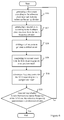
- FIG. 6 is a flow chart of a frequency calibration method in accordance with a third embodiment of the present disclosure.
- FIG. 2 shows a block diagram of the PLL.
- a PLL 2 mainly comprises a reference frequency divider 20 , a PFD (Phase-Frequency Detector) 21 , a charge pump 22 , a loop filter 23 , a VCO 24 , a main frequency divider 25 , and a frequency calibration apparatus 26 .
- PFD Phase-Frequency Detector
- the reference frequency divider 20 is coupled to the PFD 21 ; the PFD 21 is respectively coupled to the charge pump 22 and the main frequency divider 25 ; the loop filter 23 is respectively coupled to the charge pump 22 and the VCO 24 ; the main frequency divider 25 is coupled to the VCO 24 ; the frequency calibration apparatus 26 is respectively coupled to the reference frequency divider 20 , the VCO 24 and the main frequency divider 25 ; and a reference voltage V REF is coupled between the loop filter 23 and the VCO 24 .
- the reference frequency divider 20 of the PLL 2 receives a reference frequency f REF , and the VCO 24 generates an output frequency f VCO .
- the PLL 2 further comprises a first switch SW 1 , a second switch SW 2 and a third switch SW 3 .
- the first SW 1 is coupled between the loop filter 23 and the VCO 24 ;
- the second switch SW 2 is coupled between the reference voltage V REF and the VCO 24 ;
- the third switch SW 3 is for switching between a first feedback clock CKV and a second feedback clock CKV 0 to allow either of them to reach the frequency calibration apparatus 26 .
- the first feedback clock CKV is a high-speed clock
- the second feedback clock CKV 0 is a normal-speed clock, which are determined from adjusting a divisor M by the main frequency divider 25 .
- FIG. 3 shows a block diagram of the frequency calibration apparatus of the PLL 2 .
- the frequency calibration apparatus 26 comprises a frequency detecting module 260 and a binary search module 262 .
- the frequency detecting module 260 comprises a first counter 2600 , a second counter 2602 , a shifting unit 2604 , and a comparing unit 2606 .
- the first counter 2600 is coupled to the reference frequency divider 20 and the shifting unit 2604 ; the second counter 2602 is coupled to the main frequency divider 25 ; the comparing unit 2606 is coupled to the shifting unit 2604 and the second counter 2602 ; and the binary search module 262 is coupled to the first counter 2600 , the second counter 2602 and the comparing unit 2606 .
- the frequency calibration apparatus 26 of the PLL 2 is operated in a frequency locked mode.
- the first switch SW 1 is open
- the second switch SW 2 is closed
- the third switch SW 3 is coupled to the first feedback clock CKV.
- the frequency calibration apparatus 26 calibrates the output frequency f VCO outputted by the VCO 24 , so that a ratio of the output frequency f VCO and the reference frequency f REF approximates a predetermined ratio. Operations of the frequency calibration apparatus 26 in the frequency locked mode are to be discussed.
- the frequency detecting module 260 compares the reference clock CKR with the first feedback clock CKV (or the second feedback clock CKV 0 ) to generate a comparison result that is regarded as a basis for the binary search module 262 to adjust the VCO 24 .
- the reference clock CKR is generated from the reference frequency f REF by the reference frequency divider 20 according to a predetermined multiple (e.g. 1 ⁇ 4).
- the first counter 2600 generates a first count according to the reference clock CKR.
- the first feedback clock CKV and the second feedback clock CKV 0 are respectively generated from frequency dividing the output frequency f VCO of the VCO 24 by the predetermined divisor M by the main frequency divider 25 .
- the second counter 2602 generates a second count according to the first feedback clock CKV (or the second feedback CKV 0 ). More specifically, the first feedback clock CKV, a relative high-speed clock, is provided to the frequency calibration apparatus 26 in the frequency locked mode to calibrate the output frequency f VCO , so as to reduce an overall calibration time.
- the second feedback clock CKV 0 a normal-speed clock, is provided to the PFD 21 in a phase locked mode, or is provided to the frequency calibration apparatus 26 in the frequency locked mode to calibrate the output frequency f VCO , but without rendering the advantage of reducing the overall calibration time.
- the first feedback clock CKV rate is designed as a power of 2 times the reference clock CKR rate, e.g., 2, 4, 8 times, and so forth. Therefore, the shifting unit 2604 shifts the first count generated by the first counter 2600 to generate a shifted count (i.e., the first count is multiplied by the power of 2). The shifted count is transmitted to the comparing unit 16 to be compared with the second count, so that an accurate comparison result is obtained.
- the comparing unit 16 e.g., an N-bit comparing unit
- the first count is shifted by M bits by the shifting unit 2604 , i.e., M-bit zeros are complemented (i.e., the first count is multiplied by the M-th power of 2), so that the second count also has N bits to accurately determine an output frequency range of the VCO 24 .
- the reference clock CKR is a low-speed clock and the first feedback clock CKV is a high-speed clock. Therefore, the first counter 2600 of the frequency calibration apparatus 26 only needs to operate with a low-speed, instead of with the high-speed as the second counter 2602 does.
- the shifting unit 2604 may be a common shifting unit to replace the multiplier in the prior art. The foregoing design is capable of significantly reducing circuit cost of the present disclosure.
- the comparing unit 2606 compares the second count with the shifted count both having N bits to generate a comparison result. It is to be noted that, the comparing unit 2606 compares a value of the second count with that of the shifted count, such that the comparison result indicates three possible situations—(1) the second count is larger than the shifted count, (2) the second count is equal to the shifted count, and (3) the second count is smaller than the shifted count. Therefore, in order to represent the three possible situations, the comparing unit 2606 outputs the comparison result in the form of two control bits to the binary search module 262 .
- the second search module 262 is for selecting an optimal VCO frequency curve from n VCO frequency curves of the VCO 24 .
- the binary search module 262 determines one bit of the optimal VCO frequency curve every time according to the comparison result of the comparing unit 2606 , and iterates several times to determine the optimal VCO frequency curve. For example, supposing that the VCO frequency curve has 16 curves (i.e., 4-th power of 2 curves) and a predetermined VCO frequency curve is 1000, when the comparing unit 2606 generates a first comparison result, the binary search module 262 determines a most significant bit (MSB) and a second MSB according to the first comparison result, while other bits are set to “0”.
- MSB most significant bit
- the optimal frequency curve is selected and is provided to the VCO 24 to calibrate the output frequency f VCO according to the optimal frequency curve.
- the frequency calibration apparatus 26 adopts monitoring periods having different lengths when iterating the calibration procedure. More specifically, in an initial stage of the calibration procedure, when the binary search module 262 determines the MSB of the VCO frequency curve, the VCO frequency curves determined at this point are far from the optimal VCO frequency curve, and hence the comparing unit 2606 can nevertheless generate a difference even when only a short period is adopted (i.e., the first counter 2600 and the second counter 2602 only needs to perform fewer of calculations).
- the binary search module 262 determines a least significant bit (LSB) of the VCO frequency curve
- the VCO frequency curves determined at this point are approximate to the optimal VCO frequency curve, and hence the comparing unit 2606 can only generate a difference when a long period is adopted (i.e., the first counter 2600 and the second counter 2602 have to perform more calculations).
- the frequency calibration apparatus 26 determines the MSB
- a shorter monitoring period is adopted; when the frequency calibration apparatus 26 determines the LSB, a longer monitoring period is adopted.
- the bits of the optimal VCO frequency curve are accurately determined, and the overall calibration time of the frequency calibration apparatus 26 is significantly reduced, so as to effectively overcome the disadvantage that the overall calibration time is too long due to the monitoring periods having the same length as in the prior art.
- the binary search module 262 transmits a control signal to halt the first counter 2600 and the second counter 2602 , and the PLL 2 enters the phase locked mode. That is to say, the first switch SW 1 becomes closed, and the second switch SW 2 becomes open.
- FIG. 2 shows operations of the PLL 2 in the phase locked mode.
- the PFD 21 When the PLL 2 is in the phase locked mode, the PFD 21 respectively receives the reference clock CKR and the second feedback clock CKV 0 from the reference frequency divider 20 and the main frequency divider 25 , and detects a phase difference between the reference clock CKR and the feedback clock CKV 0 to selectively generate an up index UP and a down index DN.
- the charge pump 22 adjusts a control current according to the up index UP or the down index DN
- the loop filter 23 adjusts its control voltage outputted to the VCO 24 according to the control current, so that the ratio of the output frequency f VCO of the VCO 24 and the reference frequency f REF approximates the predetermined ratio.
- FIG. 4A shows a relation curve of the output frequency f VCO of the VCO 24 and a control voltage Vc.
- a predetermined control voltage Vc(center) is in the middle of a range between a minimum control voltage Vc(min) and a maximum control voltage Vc(max), and frequency curves respectively correspond to different shifted counts.
- each of the shifted counts has four control bits, such that a minimum shifted count is “0000” and a maximum shifted count is “1111”, which respectively correspond to a lower frequency limit F_L and an upper frequency limit F_H.
- areas I, area II and area III, formed by the minimum control voltage Vc(min), the maximum control voltage Vc(max), the upper frequency limit F_H and the lower frequency limit F_L, are represented by frequency curves corresponding to shifted counts “0100”, “1000” and “1100”.
- the binary search module 262 selects the frequency curve “1000”, and two frequency curves “0110” and “1010” above and below the frequency curve “1000”, as three candidate frequency curves.
- the binary search module 262 selects the frequency curve “0100”, and two frequency curves the “0110” and “0010” above and below the frequency curve “0100”, as three candidate frequency curves.
- FIG. 5 shows a schematic diagram of how to determine an optimal frequency curve by the frequency calibration apparatus 26 via several of calibration procedures. Supposing that there are eight frequency curves each having four bits, an initial frequency curve is defined as “1000”, the optimal frequency curve is “1001”, and the control bits comprise at least two bits including three statuses of being “greater than”, “equal to” and “smaller than”. Under such circumstances, the binary search module 262 performs the calibration procedure three times to determine the optimal frequency curve. More specifically, in this embodiment, the first calibration procedure and the second calibration procedure adopt a shorter monitoring period, and the third calibration procedure adopt a longer monitoring period.
- the binary search module 262 first determines a first bit and a second bit, i.e., one frequency curve is selected from the three candidate frequency curves “1000”, “1100” and “0100”. For example, when the control signal is “greater than”, the frequency curve “1100” is selected; when the control signal is “smaller than”, the frequency curve “ 0100 ” is selected; when the control signal is “equal to”, the frequency curve “1000” is selected. Since the first monitoring period is set to be a short monitoring period and the initial frequency curve “1000” approximates to the optimal frequency curve “1001”, there is no difference between the second count and the shifted count when the first monitoring period ends. Thus, the comparing unit 2606 outputs the control signal indicating the “equal to” situation, and accordingly the binary search module 262 selects the frequency curve “1000”.
- the binary search module 262 determines the second bit and a third bit, i.e., one frequency curve is selected from the three frequency curves “1000”, “1010” and “0110”. Likewise, since the second monitoring period is also set to be a short monitoring period and the current frequency curve “1000” approximates the optimal frequency curve “1001”, there is no difference between the second count and the shifted count when the second monitoring period ends. Thus, the comparing unit 2606 outputs the control signal indicating the “equal to” situation, and accordingly the binary search module 262 selects the frequency curve “1000”.
- the binary search module 262 determines the third bit and a fourth bit, i.e., one frequency curve is selected from the three frequency curves “1000”, “1001” and “0111”. Since the third calibration procedure adopts is set to be a long monitoring period, there is a difference between the second count and shifted count even when the current frequency curve “1000” approximates the optimal frequency curve “1001”. Thus, the comparing unit 2606 outputs the control signal indicating the “greater than” situation, and accordingly the binary search module 262 selects the frequency curve “1001” as a result of the optimal frequency curve “1000” obtained in the first calibration procedure due to the first comparison result indicating that the second count is equal to the shifted count. It is to be noted that, for that the frequency calibration apparatus 26 adopts monitoring periods of different time lengths each time the calibration procedure iterates, effect of reducing the calibration time becomes more obvious as the number of frequency curves gets larger.
- a method for operating a frequency calibration apparatus is provided.
- the frequency calibration apparatus is applied to a PLL and is operated in a phase locked mode.
- the PLL comprises a reference frequency divider, a main frequency divider and a VCO.
- FIG. 6 shows a flow chart of the method for operating the frequency calibration apparatus in accordance with the second embodiment of the present disclosure.
- Step S 10 a reference clock is received from the reference frequency divider and a first count is generated according to the reference clock.
- the reference clock is generated from frequency dividing a reference frequency by the reference frequency divider of the PLL.
- Step S 12 a first feedback clock is received from the main frequency divider and a second count is generated according to the first feedback clock.
- the first feedback clock is generated from frequency dividing an output frequency of the VCO by the main frequency divider of the PLL.
- the first feedback clock rate is higher than the reference clock rate, i.e., compared to the high-speed first feedback clock, a low-speed reference clock is implemented in this embodiment.
- the main frequency divider also generates a second feedback clock to the PLL, with the second feedback clock rate being lower than the first feedback clock rate. That is to say, the main frequency divider generates the faster feedback clock to the frequency calibration apparatus, and generates the slower feedback clock to the PLL.
- Step S 14 the first count is shifted to generate a shifted count.
- the first count comprises (N ⁇ M) control bits
- the second count comprises N control bits
- N and M are positive integers, where N is larger than M.
- the first count shifted by M control bits becomes the shifted count that comprises the same number of N control bits as the second count.
- Step S 16 the second count is compared with the shifted count to generate a comparison result.
- the comparison result indicates three possible situations—(1) the second count is greater than the shifted count, (2) the second count is equal to the shifted count, and (3) the second count is smaller than the shifted count.
- an optimal reference curve is selected from three candidate VCO frequency curves in response to the comparison result to calibrate an output frequency of the VCO.
- the three candidate VCO frequency curves respectively correspond to the three possible situations of the comparison result.
- Step S 10 to Step S 18 a procedure for calibrating the output frequency of the VCO is completed once.
- the method proceeds to Step S 20 in which it is determined whether a ratio between the output frequency of the VCO and the reference frequency approximates a predetermined ratio.
- the predetermined ratio is specifically limited. For example, when the predetermined ratio is equal to 1, it means that the output frequency is equal to the reference frequency.
- Step S 20 When the determination result of Step S 20 is positive, it means that the frequency calibration procedure of the PLL is completed by the frequency calibration apparatus, so that the PLL enters a phase locked mode.
- the determination result of Step S 20 is negative, it means that the ratio between the output frequency and the reference frequency does not approximate the predetermined ratio, i.e., the frequency calibration procedure of the PLL is not yet completed, such that the frequency calibration apparatus iterates Steps S 10 to S 18 until the ratio between the calibrated output frequency and the reference frequency approximates the predetermined ratio. It is to be noted that, during each iteration of the frequency calibration procedure carried out by the frequency calibration apparatus, monitoring periods of different time lengths are adopted to reduce an overall calibration time of the frequency calibration apparatus.
- a frequency calibration apparatus applied to a PLL according to the present disclosure implements a low-speed reference clock and monitoring periods of different time lengths during each iteration of a frequency calibration procedure, an overall time for calibrating by the frequency calibration apparatus a frequency of the PLL is significantly reduced.
- the frequency calibration apparatus first applies a counter to generate a count according to the low-speed reference clock, and then applies a shifting unit to shift the count, so that the counter only needs to be operated with a low-speed.
- production cost of the frequency calibration apparatus applied to the PLL according to the present disclosure is accordingly reduced to improve market competitiveness.
Landscapes
- Stabilization Of Oscillater, Synchronisation, Frequency Synthesizers (AREA)
Abstract
Description
Claims (20)
Applications Claiming Priority (3)
| Application Number | Priority Date | Filing Date | Title |
|---|---|---|---|
| TW98129821A TWI470937B (en) | 2009-09-04 | 2009-09-04 | Frequency calibration apparatus and method of phase locked loop |
| TW98129821A | 2009-09-04 | ||
| TW098129821 | 2009-09-04 |
Publications (2)
| Publication Number | Publication Date |
|---|---|
| US20110057696A1 US20110057696A1 (en) | 2011-03-10 |
| US9479184B2 true US9479184B2 (en) | 2016-10-25 |
Family
ID=43647244
Family Applications (1)
| Application Number | Title | Priority Date | Filing Date |
|---|---|---|---|
| US12/858,315 Expired - Fee Related US9479184B2 (en) | 2009-09-04 | 2010-08-17 | Frequency calibration apparatus of phase locked loop and method thereof |
Country Status (2)
| Country | Link |
|---|---|
| US (1) | US9479184B2 (en) |
| TW (1) | TWI470937B (en) |
Cited By (1)
| Publication number | Priority date | Publication date | Assignee | Title |
|---|---|---|---|---|
| US11496137B2 (en) | 2020-12-10 | 2022-11-08 | Samsung Electronics Co., Ltd. | Automatic frequency calibration and lock detection circuit and phase locked loop including te same |
Families Citing this family (10)
| Publication number | Priority date | Publication date | Assignee | Title |
|---|---|---|---|---|
| US8513992B1 (en) * | 2010-09-10 | 2013-08-20 | Integrated Device Technology, Inc. | Method and apparatus for implementation of PLL minimum frequency via voltage comparison |
| US9048850B2 (en) * | 2012-07-02 | 2015-06-02 | Qualcomm Incorporated | Frequency synthesizer apparatus and methods for improving capacitor code search accuracy using LSB modulation |
| US9065454B2 (en) * | 2012-11-29 | 2015-06-23 | Taiwan Semiconductor Manufacturing Company, Ltd. | Phase locked loop with self-calibration |
| CN107005244B (en) * | 2017-02-08 | 2020-05-05 | 香港应用科技研究院有限公司 | Gain Calibration of Direct Modulation Synthesizers Using Lookup Table Search by Decreasing Count of Overflow Counters |
| US9935640B1 (en) * | 2017-02-08 | 2018-04-03 | Hong Kong Applied Science and Technology Research Institute Company, Limited | Gain calibration for direct modulation synthesizer using a look-up table searched by a reduced count from an overflow counter |
| US10700669B2 (en) * | 2018-06-19 | 2020-06-30 | Aura Semiconductor Pvt. Ltd | Avoiding very low duty cycles in a divided clock generated by a frequency divider |
| US11070218B2 (en) * | 2019-04-17 | 2021-07-20 | Texas Instruments Incorporated | Real time counter-based method for the determination and measurement of frequency lock time in phase-locked loops |
| US10991447B2 (en) * | 2019-06-25 | 2021-04-27 | Sandisk Technologies Llc | Clock frequency counting during high-voltage operations for immediate leakage detection and response |
| US11075638B1 (en) | 2020-12-28 | 2021-07-27 | Nxp Usa, Inc. | System and method for calibrating digital phase locked loop |
| CN113285712B (en) * | 2021-04-25 | 2022-05-17 | 中国电子科技集团公司第二十九研究所 | Multi-stage VCO (voltage controlled oscillator) frequency calibration method applied to phase-locked loop |
Citations (30)
| Publication number | Priority date | Publication date | Assignee | Title |
|---|---|---|---|---|
| US4672556A (en) * | 1984-09-17 | 1987-06-09 | Sundstrand Corporation | Frequency detector system |
| US6150891A (en) * | 1998-05-29 | 2000-11-21 | Silicon Laboratories, Inc. | PLL synthesizer having phase shifted control signals |
| US6311050B1 (en) * | 1998-05-29 | 2001-10-30 | Silicon Laboratories, Inc. | Single integrated circuit phase locked loop for synthesizing high-frequency signals for wireless communications and method for operating same |
| US20020008585A1 (en) * | 1998-05-29 | 2002-01-24 | Silicon Laboratories, Inc. | Method and apparatus for synthesizing dual band high-frequency signals for wireless communications |
| US6539320B1 (en) * | 1998-12-24 | 2003-03-25 | Mitsubishi Denki Kabushiki Kaisha | Time delay determination and determination of signal shift |
| US20030171105A1 (en) * | 2002-03-06 | 2003-09-11 | Dunworth Jeremy D. | Calibration techniques for frequency synthesizers |
| US20030197564A1 (en) * | 2002-04-22 | 2003-10-23 | Humphreys Scott Robert | Coarse tuning for fractional-n synthesizers |
| US20040000956A1 (en) * | 2002-06-28 | 2004-01-01 | Rolf Jaehne | Phase-locked loop with automatic frequency tuning |
| US20040075506A1 (en) * | 1998-05-29 | 2004-04-22 | Silicon Laboratories Inc. | Method and apparatus for operating a PLL with a phase detector/sample hold circuit for synthesizing high-frequency signals for wireless communications |
| US20050083137A1 (en) * | 2003-10-18 | 2005-04-21 | Samsung Electronics Co., Ltd. | Frequency synthesizer using a wide-band voltage controlled oscillator and a fast adaptive frequency calibration method |
| US20050137816A1 (en) * | 2003-12-19 | 2005-06-23 | Chao-Shi Chuang | Method for automatically calibrating the frequency range of a pll and associated pll capable of automatic calibration |
| US7023282B1 (en) * | 2004-05-11 | 2006-04-04 | Rf Micro Devices, Inc. | Coarse tuning for fractional-N synthesizers having reduced period comparison error |
| US7064591B1 (en) * | 2004-05-11 | 2006-06-20 | Rf Micro Devices, Inc. | Coarse tuning for fractional-N synthesizers |
| US20060214737A1 (en) * | 2005-03-28 | 2006-09-28 | Texas Instruments Incorporated | Phase-locked loop with a digital calibration loop and an analog calibration loop |
| US20060269014A1 (en) * | 2005-05-27 | 2006-11-30 | Intel Corporation | Oscillator frequency selection |
| US20080015800A1 (en) * | 2006-06-22 | 2008-01-17 | Qimonda Ag | Method and system for determining frequency |
| US20080054960A1 (en) * | 2006-08-18 | 2008-03-06 | Texas Instruments Deutschland Gmbh | Phase-locked loop (pll) circuit and method |
| US20080100385A1 (en) * | 2006-11-01 | 2008-05-01 | Eric-Wei Lin | Loop system capable of auto-calibrating oscillating frequency range and related method |
| US20080195341A1 (en) * | 2007-01-18 | 2008-08-14 | International Business Machines, Inc. | System and method for determining a delay time interval of components |
| US20080297221A1 (en) * | 2007-05-29 | 2008-12-04 | Shinko Electric Industries Co., Ltd. | Delay circuit and delay time adjustment method |
| US7486147B2 (en) * | 2006-12-06 | 2009-02-03 | Broadcom Corporation | Low phase noise phase locked loops with minimum lock time |
| US20090237132A1 (en) * | 2008-03-20 | 2009-09-24 | Integrated Device Technology, Inc. | Phase-locked loop |
| US20090290717A1 (en) * | 2008-05-21 | 2009-11-26 | Yamaha Corporation | Delay time calculation apparatus, delay time calculation method, and storage medium storing program therefor |
| US20100057390A1 (en) * | 2008-08-27 | 2010-03-04 | Aerodyne Research, Inc. | System and method for precision phase shift measurement |
| US20100073048A1 (en) * | 2008-09-24 | 2010-03-25 | Mediatek Inc. | Phase locked loop and calibration method |
| US20100171535A1 (en) * | 2008-09-19 | 2010-07-08 | Hyman Shanan | Calibration system and method for phase-locked loops |
| US20100171652A1 (en) * | 2009-01-06 | 2010-07-08 | Gutt Gregory M | Local clock frequency calibration using low earth orbit (leo) satellites |
| US20100213984A1 (en) * | 2009-02-24 | 2010-08-26 | Kwangwoon University Industry-Academic Collaboration Foundation | Automatic frequency calibration apparatus and method for a phase-locked loop based frequency synthesizer |
| US20110082657A1 (en) * | 2009-10-05 | 2011-04-07 | Fujitsu Limited | Delay analysis device, delay analysis method, and delay analysis program |
| US7969248B1 (en) * | 2009-07-30 | 2011-06-28 | Lattice Semiconductor Corporation | Oscillator tuning for phase-locked loop circuit |
Family Cites Families (1)
| Publication number | Priority date | Publication date | Assignee | Title |
|---|---|---|---|---|
| US6900675B2 (en) * | 2003-09-02 | 2005-05-31 | Standard Microsystems Corporation | All digital PLL trimming circuit |
-
2009
- 2009-09-04 TW TW98129821A patent/TWI470937B/en not_active IP Right Cessation
-
2010
- 2010-08-17 US US12/858,315 patent/US9479184B2/en not_active Expired - Fee Related
Patent Citations (31)
| Publication number | Priority date | Publication date | Assignee | Title |
|---|---|---|---|---|
| US4672556A (en) * | 1984-09-17 | 1987-06-09 | Sundstrand Corporation | Frequency detector system |
| US6741846B1 (en) * | 1998-05-29 | 2004-05-25 | Silicon Laboratories Inc. | Method and apparatus for operating a PLL with a phase detector/sample hold circuit for synthesizing high-frequency signals for wireless communications |
| US6311050B1 (en) * | 1998-05-29 | 2001-10-30 | Silicon Laboratories, Inc. | Single integrated circuit phase locked loop for synthesizing high-frequency signals for wireless communications and method for operating same |
| US20020008585A1 (en) * | 1998-05-29 | 2002-01-24 | Silicon Laboratories, Inc. | Method and apparatus for synthesizing dual band high-frequency signals for wireless communications |
| US20040075506A1 (en) * | 1998-05-29 | 2004-04-22 | Silicon Laboratories Inc. | Method and apparatus for operating a PLL with a phase detector/sample hold circuit for synthesizing high-frequency signals for wireless communications |
| US6150891A (en) * | 1998-05-29 | 2000-11-21 | Silicon Laboratories, Inc. | PLL synthesizer having phase shifted control signals |
| US6539320B1 (en) * | 1998-12-24 | 2003-03-25 | Mitsubishi Denki Kabushiki Kaisha | Time delay determination and determination of signal shift |
| US20030171105A1 (en) * | 2002-03-06 | 2003-09-11 | Dunworth Jeremy D. | Calibration techniques for frequency synthesizers |
| US20030197564A1 (en) * | 2002-04-22 | 2003-10-23 | Humphreys Scott Robert | Coarse tuning for fractional-n synthesizers |
| US20040000956A1 (en) * | 2002-06-28 | 2004-01-01 | Rolf Jaehne | Phase-locked loop with automatic frequency tuning |
| US20050083137A1 (en) * | 2003-10-18 | 2005-04-21 | Samsung Electronics Co., Ltd. | Frequency synthesizer using a wide-band voltage controlled oscillator and a fast adaptive frequency calibration method |
| US20050137816A1 (en) * | 2003-12-19 | 2005-06-23 | Chao-Shi Chuang | Method for automatically calibrating the frequency range of a pll and associated pll capable of automatic calibration |
| US7023282B1 (en) * | 2004-05-11 | 2006-04-04 | Rf Micro Devices, Inc. | Coarse tuning for fractional-N synthesizers having reduced period comparison error |
| US7064591B1 (en) * | 2004-05-11 | 2006-06-20 | Rf Micro Devices, Inc. | Coarse tuning for fractional-N synthesizers |
| US20060214737A1 (en) * | 2005-03-28 | 2006-09-28 | Texas Instruments Incorporated | Phase-locked loop with a digital calibration loop and an analog calibration loop |
| US20060269014A1 (en) * | 2005-05-27 | 2006-11-30 | Intel Corporation | Oscillator frequency selection |
| US20080015800A1 (en) * | 2006-06-22 | 2008-01-17 | Qimonda Ag | Method and system for determining frequency |
| US20080054960A1 (en) * | 2006-08-18 | 2008-03-06 | Texas Instruments Deutschland Gmbh | Phase-locked loop (pll) circuit and method |
| US20080100385A1 (en) * | 2006-11-01 | 2008-05-01 | Eric-Wei Lin | Loop system capable of auto-calibrating oscillating frequency range and related method |
| US7486147B2 (en) * | 2006-12-06 | 2009-02-03 | Broadcom Corporation | Low phase noise phase locked loops with minimum lock time |
| US20080195341A1 (en) * | 2007-01-18 | 2008-08-14 | International Business Machines, Inc. | System and method for determining a delay time interval of components |
| US20080297221A1 (en) * | 2007-05-29 | 2008-12-04 | Shinko Electric Industries Co., Ltd. | Delay circuit and delay time adjustment method |
| US20090237132A1 (en) * | 2008-03-20 | 2009-09-24 | Integrated Device Technology, Inc. | Phase-locked loop |
| US20090290717A1 (en) * | 2008-05-21 | 2009-11-26 | Yamaha Corporation | Delay time calculation apparatus, delay time calculation method, and storage medium storing program therefor |
| US20100057390A1 (en) * | 2008-08-27 | 2010-03-04 | Aerodyne Research, Inc. | System and method for precision phase shift measurement |
| US20100171535A1 (en) * | 2008-09-19 | 2010-07-08 | Hyman Shanan | Calibration system and method for phase-locked loops |
| US20100073048A1 (en) * | 2008-09-24 | 2010-03-25 | Mediatek Inc. | Phase locked loop and calibration method |
| US20100171652A1 (en) * | 2009-01-06 | 2010-07-08 | Gutt Gregory M | Local clock frequency calibration using low earth orbit (leo) satellites |
| US20100213984A1 (en) * | 2009-02-24 | 2010-08-26 | Kwangwoon University Industry-Academic Collaboration Foundation | Automatic frequency calibration apparatus and method for a phase-locked loop based frequency synthesizer |
| US7969248B1 (en) * | 2009-07-30 | 2011-06-28 | Lattice Semiconductor Corporation | Oscillator tuning for phase-locked loop circuit |
| US20110082657A1 (en) * | 2009-10-05 | 2011-04-07 | Fujitsu Limited | Delay analysis device, delay analysis method, and delay analysis program |
Cited By (1)
| Publication number | Priority date | Publication date | Assignee | Title |
|---|---|---|---|---|
| US11496137B2 (en) | 2020-12-10 | 2022-11-08 | Samsung Electronics Co., Ltd. | Automatic frequency calibration and lock detection circuit and phase locked loop including te same |
Also Published As
| Publication number | Publication date |
|---|---|
| TWI470937B (en) | 2015-01-21 |
| US20110057696A1 (en) | 2011-03-10 |
| TW201110561A (en) | 2011-03-16 |
Similar Documents
| Publication | Publication Date | Title |
|---|---|---|
| US9479184B2 (en) | Frequency calibration apparatus of phase locked loop and method thereof | |
| US8183950B2 (en) | Auto-calibration for ring oscillator VCO | |
| US9042854B2 (en) | Apparatus and methods for tuning a voltage controlled oscillator | |
| US7948286B2 (en) | Bandwidth control apparatus for phase lock loop and method thereof | |
| US8750448B2 (en) | Frequency calibration apparatus of frequency synthesizer and frequency calibration method thereof | |
| WO2018145326A1 (en) | Gain calibration for direct modulation synthesizer using look-up table searched by reduced count from overflow counter | |
| US8004367B2 (en) | VCO control and methods therefor | |
| TW200935746A (en) | Dynamic biasing of a VCO in a phase-locked loop | |
| US11356108B2 (en) | Frequency generator and associated method | |
| US7859346B2 (en) | Clock generator and associated self-test and switching-control method | |
| US11070215B2 (en) | Locked loop circuit and method with digitally-controlled oscillator (DCO) gain normalization | |
| US12483254B2 (en) | Automatic hybrid oscillator gain adjustor circuit | |
| CN100426674C (en) | Fast frequency locking device, frequency synthesizer and fast frequency locking method | |
| US7548124B2 (en) | System and method for self calibrating voltage-controlled oscillator | |
| US8629728B2 (en) | VCO control circuit and method thereof, fast locking PLL and method for fast locking PLL | |
| US8509372B1 (en) | Multi-band clock generator with adaptive frequency calibration and enhanced frequency locking | |
| US20150130544A1 (en) | Method and apparatus to calibrate frequency synthesizer | |
| US10270487B2 (en) | Frequency generator and associated method | |
| US20080157879A1 (en) | Decreasing frequency synthesizer lock time for a phase locked loop | |
| US11496139B2 (en) | Frequency measurement circuit with adaptive accuracy | |
| JP4807156B2 (en) | Voltage controlled oscillator and control method thereof | |
| CN102013888A (en) | Frequency correction device of phase-locked loop and operating method thereof | |
| EP2797224A1 (en) | PLL direct modulator and frequency gain mismatch compensation method in the modulator | |
| JP4105169B2 (en) | Frequency synthesizer, radio communication system using the same, and control method of frequency synthesizer | |
| CN117176146A (en) | Method for improving frequency hopping speed and application |
Legal Events
| Date | Code | Title | Description |
|---|---|---|---|
| AS | Assignment |
Owner name: MSTAR SEMICONDUCTOR, INC., TAIWAN Free format text: ASSIGNMENT OF ASSIGNORS INTEREST;ASSIGNORS:HSIEH, MING-YU;YEN, SHIH-CHIEH;WANG, YAO-CHI;SIGNING DATES FROM 20100525 TO 20100617;REEL/FRAME:024848/0888 |
|
| FEPP | Fee payment procedure |
Free format text: PAYOR NUMBER ASSIGNED (ORIGINAL EVENT CODE: ASPN); ENTITY STATUS OF PATENT OWNER: LARGE ENTITY |
|
| ZAAA | Notice of allowance and fees due |
Free format text: ORIGINAL CODE: NOA |
|
| ZAAB | Notice of allowance mailed |
Free format text: ORIGINAL CODE: MN/=. |
|
| STCF | Information on status: patent grant |
Free format text: PATENTED CASE |
|
| AS | Assignment |
Owner name: MEDIATEK INC., TAIWAN Free format text: MERGER;ASSIGNOR:MSTAR SEMICONDUCTOR, INC.;REEL/FRAME:052381/0368 Effective date: 20190115 |
|
| MAFP | Maintenance fee payment |
Free format text: PAYMENT OF MAINTENANCE FEE, 4TH YEAR, LARGE ENTITY (ORIGINAL EVENT CODE: M1551); ENTITY STATUS OF PATENT OWNER: LARGE ENTITY Year of fee payment: 4 |
|
| AS | Assignment |
Owner name: XUESHAN TECHNOLOGIES INC., CANADA Free format text: ASSIGNMENT OF ASSIGNORS INTEREST;ASSIGNOR:MEDIATEK INC.;REEL/FRAME:055486/0870 Effective date: 20201223 |
|
| FEPP | Fee payment procedure |
Free format text: MAINTENANCE FEE REMINDER MAILED (ORIGINAL EVENT CODE: REM.); ENTITY STATUS OF PATENT OWNER: LARGE ENTITY |
|
| LAPS | Lapse for failure to pay maintenance fees |
Free format text: PATENT EXPIRED FOR FAILURE TO PAY MAINTENANCE FEES (ORIGINAL EVENT CODE: EXP.); ENTITY STATUS OF PATENT OWNER: LARGE ENTITY |
|
| STCH | Information on status: patent discontinuation |
Free format text: PATENT EXPIRED DUE TO NONPAYMENT OF MAINTENANCE FEES UNDER 37 CFR 1.362 |
|
| FP | Lapsed due to failure to pay maintenance fee |
Effective date: 20241025 |