US9478662B2 - Gate and source/drain contact structures for a semiconductor device - Google Patents
Gate and source/drain contact structures for a semiconductor device Download PDFInfo
- Publication number
- US9478662B2 US9478662B2 US15/063,604 US201615063604A US9478662B2 US 9478662 B2 US9478662 B2 US 9478662B2 US 201615063604 A US201615063604 A US 201615063604A US 9478662 B2 US9478662 B2 US 9478662B2
- Authority
- US
- United States
- Prior art keywords
- conductive contact
- dielectric spacer
- source
- conductive
- contact
- Prior art date
- Legal status (The legal status is an assumption and is not a legal conclusion. Google has not performed a legal analysis and makes no representation as to the accuracy of the status listed.)
- Active
Links
- 239000004065 semiconductor Substances 0.000 title claims description 36
- 125000006850 spacer group Chemical group 0.000 claims abstract description 67
- 239000000463 material Substances 0.000 claims description 20
- 239000000758 substrate Substances 0.000 claims description 18
- 229910052751 metal Inorganic materials 0.000 claims description 17
- 239000002184 metal Substances 0.000 claims description 17
- 239000010410 layer Substances 0.000 description 58
- 238000000034 method Methods 0.000 description 54
- 230000008569 process Effects 0.000 description 34
- 238000001465 metallisation Methods 0.000 description 8
- 239000003989 dielectric material Substances 0.000 description 7
- 238000005137 deposition process Methods 0.000 description 6
- 238000004519 manufacturing process Methods 0.000 description 6
- XUIMIQQOPSSXEZ-UHFFFAOYSA-N Silicon Chemical compound [Si] XUIMIQQOPSSXEZ-UHFFFAOYSA-N 0.000 description 5
- 238000002955 isolation Methods 0.000 description 5
- 229910052710 silicon Inorganic materials 0.000 description 5
- 239000010703 silicon Substances 0.000 description 5
- RYGMFSIKBFXOCR-UHFFFAOYSA-N Copper Chemical compound [Cu] RYGMFSIKBFXOCR-UHFFFAOYSA-N 0.000 description 4
- VYPSYNLAJGMNEJ-UHFFFAOYSA-N Silicium dioxide Chemical compound O=[Si]=O VYPSYNLAJGMNEJ-UHFFFAOYSA-N 0.000 description 4
- 229910052802 copper Inorganic materials 0.000 description 4
- 239000010949 copper Substances 0.000 description 4
- 239000011229 interlayer Substances 0.000 description 4
- 238000012856 packing Methods 0.000 description 4
- 229910021417 amorphous silicon Inorganic materials 0.000 description 3
- 238000009413 insulation Methods 0.000 description 3
- 238000011112 process operation Methods 0.000 description 3
- 238000012545 processing Methods 0.000 description 3
- 230000004888 barrier function Effects 0.000 description 2
- 230000008901 benefit Effects 0.000 description 2
- 239000004020 conductor Substances 0.000 description 2
- 230000003247 decreasing effect Effects 0.000 description 2
- 238000011161 development Methods 0.000 description 2
- 230000018109 developmental process Effects 0.000 description 2
- 238000005516 engineering process Methods 0.000 description 2
- 239000011810 insulating material Substances 0.000 description 2
- 238000012986 modification Methods 0.000 description 2
- 230000004048 modification Effects 0.000 description 2
- 229910021420 polycrystalline silicon Inorganic materials 0.000 description 2
- 229920005591 polysilicon Polymers 0.000 description 2
- 229910021332 silicide Inorganic materials 0.000 description 2
- FVBUAEGBCNSCDD-UHFFFAOYSA-N silicide(4-) Chemical compound [Si-4] FVBUAEGBCNSCDD-UHFFFAOYSA-N 0.000 description 2
- 235000012239 silicon dioxide Nutrition 0.000 description 2
- 239000000377 silicon dioxide Substances 0.000 description 2
- WFKWXMTUELFFGS-UHFFFAOYSA-N tungsten Chemical compound [W] WFKWXMTUELFFGS-UHFFFAOYSA-N 0.000 description 2
- 229910052721 tungsten Inorganic materials 0.000 description 2
- 239000010937 tungsten Substances 0.000 description 2
- 229910052581 Si3N4 Inorganic materials 0.000 description 1
- 229910000577 Silicon-germanium Inorganic materials 0.000 description 1
- ATJFFYVFTNAWJD-UHFFFAOYSA-N Tin Chemical compound [Sn] ATJFFYVFTNAWJD-UHFFFAOYSA-N 0.000 description 1
- LEVVHYCKPQWKOP-UHFFFAOYSA-N [Si].[Ge] Chemical compound [Si].[Ge] LEVVHYCKPQWKOP-UHFFFAOYSA-N 0.000 description 1
- 230000004323 axial length Effects 0.000 description 1
- 230000015572 biosynthetic process Effects 0.000 description 1
- 230000000295 complement effect Effects 0.000 description 1
- 238000010276 construction Methods 0.000 description 1
- 238000013461 design Methods 0.000 description 1
- 239000002019 doping agent Substances 0.000 description 1
- 230000000694 effects Effects 0.000 description 1
- 239000007772 electrode material Substances 0.000 description 1
- 125000001475 halogen functional group Chemical group 0.000 description 1
- 239000007943 implant Substances 0.000 description 1
- 239000012212 insulator Substances 0.000 description 1
- 238000001459 lithography Methods 0.000 description 1
- 229910044991 metal oxide Inorganic materials 0.000 description 1
- 150000004706 metal oxides Chemical class 0.000 description 1
- 238000013508 migration Methods 0.000 description 1
- 230000005012 migration Effects 0.000 description 1
- 239000000203 mixture Substances 0.000 description 1
- 239000002070 nanowire Substances 0.000 description 1
- TWNQGVIAIRXVLR-UHFFFAOYSA-N oxo(oxoalumanyloxy)alumane Chemical compound O=[Al]O[Al]=O TWNQGVIAIRXVLR-UHFFFAOYSA-N 0.000 description 1
- 230000003071 parasitic effect Effects 0.000 description 1
- HQVNEWCFYHHQES-UHFFFAOYSA-N silicon nitride Chemical compound N12[Si]34N5[Si]62N3[Si]51N64 HQVNEWCFYHHQES-UHFFFAOYSA-N 0.000 description 1
- 238000003860 storage Methods 0.000 description 1
Images


Classifications
-
- H—ELECTRICITY
- H01—ELECTRIC ELEMENTS
- H01L—SEMICONDUCTOR DEVICES NOT COVERED BY CLASS H10
- H01L29/00—Semiconductor devices adapted for rectifying, amplifying, oscillating or switching, or capacitors or resistors with at least one potential-jump barrier or surface barrier, e.g. PN junction depletion layer or carrier concentration layer; Details of semiconductor bodies or of electrodes thereof ; Multistep manufacturing processes therefor
- H01L29/66—Types of semiconductor device ; Multistep manufacturing processes therefor
- H01L29/68—Types of semiconductor device ; Multistep manufacturing processes therefor controllable by only the electric current supplied, or only the electric potential applied, to an electrode which does not carry the current to be rectified, amplified or switched
- H01L29/76—Unipolar devices, e.g. field effect transistors
- H01L29/772—Field effect transistors
- H01L29/78—Field effect transistors with field effect produced by an insulated gate
- H01L29/785—Field effect transistors with field effect produced by an insulated gate having a channel with a horizontal current flow in a vertical sidewall of a semiconductor body, e.g. FinFET, MuGFET
-
- H—ELECTRICITY
- H01—ELECTRIC ELEMENTS
- H01L—SEMICONDUCTOR DEVICES NOT COVERED BY CLASS H10
- H01L21/00—Processes or apparatus adapted for the manufacture or treatment of semiconductor or solid state devices or of parts thereof
- H01L21/70—Manufacture or treatment of devices consisting of a plurality of solid state components formed in or on a common substrate or of parts thereof; Manufacture of integrated circuit devices or of parts thereof
- H01L21/71—Manufacture of specific parts of devices defined in group H01L21/70
- H01L21/768—Applying interconnections to be used for carrying current between separate components within a device comprising conductors and dielectrics
- H01L21/76801—Applying interconnections to be used for carrying current between separate components within a device comprising conductors and dielectrics characterised by the formation and the after-treatment of the dielectrics, e.g. smoothing
- H01L21/76802—Applying interconnections to be used for carrying current between separate components within a device comprising conductors and dielectrics characterised by the formation and the after-treatment of the dielectrics, e.g. smoothing by forming openings in dielectrics
- H01L21/76816—Aspects relating to the layout of the pattern or to the size of vias or trenches
-
- H—ELECTRICITY
- H01—ELECTRIC ELEMENTS
- H01L—SEMICONDUCTOR DEVICES NOT COVERED BY CLASS H10
- H01L21/00—Processes or apparatus adapted for the manufacture or treatment of semiconductor or solid state devices or of parts thereof
- H01L21/70—Manufacture or treatment of devices consisting of a plurality of solid state components formed in or on a common substrate or of parts thereof; Manufacture of integrated circuit devices or of parts thereof
- H01L21/71—Manufacture of specific parts of devices defined in group H01L21/70
- H01L21/768—Applying interconnections to be used for carrying current between separate components within a device comprising conductors and dielectrics
- H01L21/76801—Applying interconnections to be used for carrying current between separate components within a device comprising conductors and dielectrics characterised by the formation and the after-treatment of the dielectrics, e.g. smoothing
- H01L21/76829—Applying interconnections to be used for carrying current between separate components within a device comprising conductors and dielectrics characterised by the formation and the after-treatment of the dielectrics, e.g. smoothing characterised by the formation of thin functional dielectric layers, e.g. dielectric etch-stop, barrier, capping or liner layers
- H01L21/76831—Applying interconnections to be used for carrying current between separate components within a device comprising conductors and dielectrics characterised by the formation and the after-treatment of the dielectrics, e.g. smoothing characterised by the formation of thin functional dielectric layers, e.g. dielectric etch-stop, barrier, capping or liner layers in via holes or trenches, e.g. non-conductive sidewall liners
-
- H—ELECTRICITY
- H01—ELECTRIC ELEMENTS
- H01L—SEMICONDUCTOR DEVICES NOT COVERED BY CLASS H10
- H01L21/00—Processes or apparatus adapted for the manufacture or treatment of semiconductor or solid state devices or of parts thereof
- H01L21/70—Manufacture or treatment of devices consisting of a plurality of solid state components formed in or on a common substrate or of parts thereof; Manufacture of integrated circuit devices or of parts thereof
- H01L21/71—Manufacture of specific parts of devices defined in group H01L21/70
- H01L21/768—Applying interconnections to be used for carrying current between separate components within a device comprising conductors and dielectrics
- H01L21/76897—Formation of self-aligned vias or contact plugs, i.e. involving a lithographically uncritical step
-
- H—ELECTRICITY
- H01—ELECTRIC ELEMENTS
- H01L—SEMICONDUCTOR DEVICES NOT COVERED BY CLASS H10
- H01L29/00—Semiconductor devices adapted for rectifying, amplifying, oscillating or switching, or capacitors or resistors with at least one potential-jump barrier or surface barrier, e.g. PN junction depletion layer or carrier concentration layer; Details of semiconductor bodies or of electrodes thereof ; Multistep manufacturing processes therefor
- H01L29/40—Electrodes ; Multistep manufacturing processes therefor
- H01L29/43—Electrodes ; Multistep manufacturing processes therefor characterised by the materials of which they are formed
- H01L29/45—Ohmic electrodes
-
- H—ELECTRICITY
- H01—ELECTRIC ELEMENTS
- H01L—SEMICONDUCTOR DEVICES NOT COVERED BY CLASS H10
- H01L2924/00—Indexing scheme for arrangements or methods for connecting or disconnecting semiconductor or solid-state bodies as covered by H01L24/00
- H01L2924/0001—Technical content checked by a classifier
- H01L2924/0002—Not covered by any one of groups H01L24/00, H01L24/00 and H01L2224/00
Definitions
- the present disclosure generally relates to the fabrication of integrated circuits, and, more particularly, to various methods of forming contacts on semiconductor devices and the resulting gate and source/drain contact structures on such semiconductor devices.
- Transistors come in a variety of shapes and forms, e.g., planar transistors, FinFET transistors, nanowire devices, etc.
- the transistors are typically either NMOS (NFET) or PMOS (PFET) type devices wherein the “N” and “P” designation is based upon the type of dopants used to create the source/drain regions of the devices.
- CMOS Complementary Metal Oxide Semiconductor
- CMOS Complementary Metal Oxide Semiconductor
- each device comprises drain and source regions and a gate electrode structure positioned above and between the source/drain regions.
- a gate electrode structure positioned above and between the source/drain regions.
- a conductive channel region forms between the drain region and the source region.
- FIG. 1 is a perspective view of an illustrative prior art FinFET semiconductor device 100 that is formed above a semiconductor substrate 105 at an intermediate point during fabrication.
- the FinFET device 100 includes three illustrative fins 110 , a gate structure 115 , sidewall spacers 120 , a gate cap layer 125 , and an isolation material 130 .
- the fins 110 have a three-dimensional configuration: a height, a width, and an axial length.
- the portions of the fins 110 covered by the gate structure 115 are the channel regions of the FinFET device 100 , while the portions of the fins 110 positioned laterally outside of the spacers 120 are part of the source/drain regions of the device 100 .
- the portions of the fins 110 in the source/drain regions may have additional epi semiconductor material formed thereon in either a merged or unmerged condition.
- the electrical connections of the individual circuit elements cannot be established within the same device level on which the circuit elements are manufactured, but require one or more additional metallization layers, which generally include metal-containing lines providing the intra-level electrical connection, and also include a plurality of inter-level connections or vertical connections, which are also referred to as vias.
- additional metallization layers which generally include metal-containing lines providing the intra-level electrical connection, and also include a plurality of inter-level connections or vertical connections, which are also referred to as vias.
- These vertical interconnect structures comprise an appropriate metal and provide the electrical connection of the various stacked metallization layers.
- an appropriate vertical contact structure is provided, a first end of which is connected to a respective contact region of a circuit element, such as a gate electrode and/or the drain and source regions of transistors, and a second end that is connected to a respective metal line in the metallization layer by a conductive via.
- the second end of the contact structure may be connected to a contact region of a further semiconductor-based circuit element, in which case the interconnect structure in the contact level is also referred to as a local interconnect.
- the contact structure may comprise contact elements or contact plugs having a generally square-like or round shape that are formed in an interlayer dielectric material, which in turn encloses and passivates the circuit elements.
- the critical dimensions of the circuit elements in the device level decreased, the dimensions of metal lines, vias and contact elements were also reduced.
- the increased packing density mandated the use of sophisticated metal-containing materials and dielectric materials in order to reduce the parasitic capacitance in the metallization layers and provide a sufficiently high conductivity of the individual metal lines and vias.
- dielectric materials which are to be understood as dielectric materials having a dielectric constant of approximately 3.0 or less, are typically used in order to achieve the required electrical performance and the electromigration behavior as is required in view of reliability of the integrated circuits. Consequently, in lower-lying metallization levels, metal lines and vias having critical dimensions of approximately 100 nm and significantly less may have to be provided in order to achieve the required packing density in accordance with density of circuit elements in the device level.
- the conductive contact elements in the contact level have to be provided with critical dimensions in the same order of magnitude.
- the contact elements typically represent plugs or line-type features, which are formed of an appropriate metal or metal composition, wherein, in sophisticated semiconductor devices, tungsten, in combination with appropriate barrier materials, has proven to be a viable contact metal.
- the interlayer dielectric material is formed first and is patterned so as to receive contact openings, which extend through the interlayer dielectric material to the corresponding contact areas of the circuit elements.
- the lateral size of the drain and source areas which defines the available area for the contact regions, may be about 100 nm and significantly less, thereby requiring extremely complex lithography and etch techniques in order to form the contact openings with well-defined lateral dimensions and with a high degree of alignment accuracy.
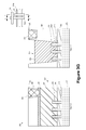
- FIG. 2 is a simplistic plan view of an illustrative prior art FinFET device 200 that will be referenced to discuss one particular problem as it relates to the formation of contact structures on a FinFET device.
- the FinFET device 200 is formed above an active region 205 that is defined in a semiconductor substrate by an isolation structure (not shown), such as a shallow trench isolation structure.
- the FinFET device 200 is comprised of three illustrative fins 210 and an illustrative gate structure 215 .
- a sidewall spacer 215 A and a gate cap layer 215 B may be formed so as to encapsulate the gate structure 215 .
- the fins 210 may be either merged on unmerged.
- the fins 210 are unmerged.
- the portions of the fins 210 positioned laterally outside of the spacers 215 A constitute the source/drain (S/D) regions of the device 200 .
- S/D source/drain
- illustrative source/drain contact structures 220 which are line-type structures that are sometimes referred to as “trench silicide” or “TS” or “CA” structures
- a gate contact structure 225 which is sometimes referred to as a “CB” structure.
- the source/drain contact structures 220 may be formed as a line-type structure to ensure, to the extent possible, good contact is achieved with all of the exterior surfaces of all of the fins 210 , even when assuming a “worst-case” misalignment scenario.
- the line-type source/drain contact structures 220 extend across the entire width 230 of the active region 205 in the gate-width direction 230 of the device 200 .
- the space 235 between the gate contact structure 225 and the source/drain contact structures 220 must be large enough such that a short circuit cannot form between the gate contact structure 225 and one of the line-type source/drain contact structures 220 .
- the distance 235 may be very small, and accordingly, the distance 240 between the active region 205 and the gate contact structure 225 may be set to be about 30-60 nm.
- One way to ensure that such a short circuit is not created would be to simply increase the distance 240 , i.e., position the gate contact structure 225 farther away from the ends of line-type source/drain contact structures 220 .
- the present disclosure is directed to various methods of forming contacts on FinFET semiconductor devices, and the resulting semiconductor devices, that may avoid, or at least reduce, the effects of one or more of the problems identified above.
- One method of forming a transistor device comprised of a source/drain region and a gate structure includes forming a dielectric layer above the source/drain region and the gate structure.
- a first opening is formed in at least the dielectric layer to expose the gate structure.
- a first spacer is formed on sidewalls of the first opening.
- a second opening is formed in at least the dielectric later to expose a portion of the source/drain region.
- the first spacer at least partially defines a spacing between the first opening and the second opening.
- a conductive gate contact is formed in the first opening and a conductive source/drain contact is formed in the second opening.
- Another illustrative method disclosed herein includes, among other things, forming a dielectric layer above a gate electrode and a source/drain region.
- a first opening is formed in at least the dielectric layer to expose the gate electrode.
- a first spacer is formed on sidewalls of the first opening.
- a second opening is formed in at least the dielectric layer to expose the source/drain region. The first spacer at least partially defines a spacing between the first opening and the second opening.
- a first conductive contact is formed in the first opening and a second conductive contact is formed in the second opening.
- One illustrative device disclosed herein includes, among other things, a substrate, a source/drain region defined in the substrate and a gate structure.
- a dielectric layer is disposed above the source/drain region and the gate structure.
- a first conductive contact is positioned in the dielectric layer and contacts the gate structure.
- a first spacer is disposed on a sidewall of the first conductive contact.
- a second conductive contact is positioned in the dielectric layer and contacts the source/drain region. The first spacer at least partially defines a spacing between the first conductive contact and the second conductive contact.
- FIG. 1 is a perspective view of one illustrative embodiment of a prior art FinFET device
- FIG. 2 is a simplistic plan view of one illustrative embodiment of a prior art FinFET device with various contact structures formed on the device;
- FIGS. 3A-3K depict one illustrative method disclosed for forming contacts on FinFET semiconductor devices and the resulting semiconductor devices;
- FIGS. 4A-4B depict an alternative process flow for forming contacts on FinFET semiconductor devices and the resulting semiconductor devices.
- FIGS. 5A-5C depict another alternative process flow for forming contacts on FinFET semiconductor devices and the resulting semiconductor devices.
- the present disclosure generally relates to various methods of forming contacts on FinFET semiconductor devices and the resulting semiconductor devices. Moreover, as will be readily apparent to those skilled in the art upon a complete reading of the present application, the present method is applicable to a variety of devices, including, but not limited to, logic devices, memory devices, etc., and the methods disclosed herein may be employed to form N-type or P-type semiconductor devices. The methods and devices disclosed herein may be employed in manufacturing products using a variety of technologies, e.g., NMOS, PMOS, CMOS, etc., and they may be employed in manufacturing a variety of different devices, e.g., memory devices, logic devices, ASICs, etc.
- technologies e.g., NMOS, PMOS, CMOS, etc.
- the inventions disclosed herein may be employed in forming integrated circuit products using a variety of so-called 3D devices, such as FinFETs.
- 3D devices such as FinFETs.
- the inventions will be disclosed in the context of forming the gate structures using a replacement gate (“gate-last”) processing technique.
- gate-last replacement gate
- the methods, structures and products disclosed herein may be employed where the gate structures of the transistors are formed using so-called “gate-first” processing techniques.
- the inventions disclosed herein should not be considered to be limited to the illustrative examples depicted and described herein.
- various illustrative embodiments of the methods and devices disclosed herein will now be described in more detail.
- FIGS. 3A-3K depict one illustrative method disclosed for forming contacts for FinFET semiconductor devices and the resulting semiconductor devices.
- the illustrative device 300 is formed in and above a semiconductor substrate 305 .
- the device 300 may be either an NMOS or a PMOS transistor or a combination thereof with a shared gate structure. Additionally, various doped regions, e.g., source/drain regions, halo implant regions, well regions and the like, are also not depicted in the attached drawings.
- the substrate 305 may have a variety of configurations, such as the depicted bulk silicon configuration.
- the substrate 305 may also have a silicon-on-insulator (SOI) configuration that includes a bulk silicon layer, a buried insulation layer and an active layer, wherein semiconductor devices are formed in and above the active layer.
- SOI silicon-on-insulator
- the substrate 305 may be made of silicon or it may be made of materials other than silicon.
- substrate or “semiconductor substrate” should be understood to cover all semiconducting materials and all forms of such materials.
- FIGS. 3A-3J also include a simplistic plan view of the device 300 (in the upper right corner) that depicts the location where various cross-sectional views depicted in the following drawings will be taken. More specifically, the view “X-X” is taken along the long axis of a gate structure of the device 300 (i.e., in the gate width direction of the device), and the view “Y-Y” is a cross-sectional view that is taken through the source/drain region of the device in a direction that is transverse to the long axis of the fins or parallel to the gate width direction of the device.
- FIG. 3A depicts the device 300 at a point in fabrication wherein several process operations have been performed.
- a plurality of trenches 302 were formed in the substrate 305 to thereby define a plurality of fins 310 .
- the illustrative FinFET device 300 disclosed herein will be depicted as being comprised of three illustrative fins 310 .
- the methods and devices disclosed herein may be employed when manufacturing FinFET devices having any number of fins.
- the illustrative example includes forming contacts for a FinFET transistor device, it may also be applied to other devices, such as planar transistor devices, or other devices.
- a recessed layer of insulating material 315 (e.g., silicon dioxide) was formed between the fins 310 to serve as an isolation structure.
- a gate structure 320 was then formed above a section of the fins 310 to define a channel region of the device 300 .
- the gate structure 320 includes a gate insulation layer 325 (e.g., a layer of high-k insulating material or silicon dioxide), and one or more conductive material layers (e.g., metal and/or polysilicon) that serve as the gate electrode 327 for the device 100 .
- the gate structure 320 may be formed using a replacement gate or “gate-last” technique (e.g., where a placeholder material is replaced with a metal gate electrode) or a “gate-first” technique (e.g., where the gate insulation layer and a gate electrode material, such as doped polysilicon, are deposited in a stack and patterned). Also depicted is an illustrative gate cap layer 330 (e.g., silicon nitride) formed above the gate structure 320 .
- a replacement gate or “gate-last” technique e.g., where a placeholder material is replaced with a metal gate electrode
- a “gate-first” technique e.g., where the gate insulation layer and a gate electrode material, such as doped polysilicon, are deposited in a stack and patterned.
- an illustrative gate cap layer 330 e.g., silicon nitride
- an optional epitaxial growth process was performed to form additional epitaxial semiconductor material 335 (e.g., silicon or silicon germanium) on the exposed surfaces of the fins 310 extending above the isolation structure 315 in the source/drain regions of the device 300 .
- additional epitaxial semiconductor material 335 e.g., silicon or silicon germanium
- the generally diamond-shaped nature of the epitaxial semiconductor material 335 results from the particular characteristics of the epitaxial growth process and the orientation of the crystallographic planes in the substrate 305 .
- a dashed-line 310 X reflects the outline of the original fins 310 in the source/drain regions of the device 300 .
- the epitaxial growth process is typically performed to increase the size of the material to which a conductive contact will later be formed.
- a so-called fin-merger epitaxial growth process is performed such that the epitaxial material grown on one fin 310 merges into the epitaxial material grown on an adjacent fin. Such merged fins are not depicted in the drawings.
- An interlayer dielectric (ILD) layer 345 is formed above the device 300 as part of a metallization system for establishing electrical contacts to the source/drain regions with the device 300 .
- FIG. 3B depicts the device 300 after several etch processes were performed.
- a masked etch process was performed through a patterned etch mask (not shown) to define a gate contact opening 350 in the ILD layer 345 above the gate structure 320 .
- the masked etch process was terminated on the gate cap layer 330 and terminates within the ILD layer 345 above the source/drain regions of the device 300 .
- One or more additional etch processes were performed to remove the portions of the gate cap layer 330 exposed by the gate contact opening 350 to thereby extend the gate contact opening 350 to expose the gate electrode 327 . Additionally, unless specifically noted otherwise, no attempt is made to show the various processing steps discussed herein in the simplistic plan views depicted in the drawings.
- FIG. 3C illustrates the device 300 after a first deposition process was performed to form a spacer layer 355 in the gate contact opening 350 and a second deposition process was performed to form a sacrificial layer 360 (e.g., amorphous silicon or aluminum oxide) above the spacer layer 355 .
- a sacrificial layer 360 e.g., amorphous silicon or aluminum oxide
- FIG. 3D illustrates the device 300 after a planarizing process, e.g., a CMP process, was performed to remove portions of the spacer layer 355 and the sacrificial layer 360 extending beyond the gate contact opening 350 .
- a planarizing process e.g., a CMP process
- FIG. 3E illustrates the device 300 after a patterned etch mask layer 365 (e.g., organic dielectric material) was formed above the ILD layer 345 and patterned to define an opening 370 above the fins 310 in the source/drain regions.
- a patterned etch mask layer 365 e.g., organic dielectric material
- an edge 370 E of the opening 370 is disposed above the spacer layer 355 .
- FIG. 3F illustrates the device 300 after a selective etch process was performed to define a fin contact opening 375 in the ILD layer 345 .
- the etch process in FIG. 3F etches oxide, but is selective to SiN and a-Si, such that even if the CA region is overlapped with the CB region due to overlay error, the regions will still be separated by the spacer layer 355 . Please note that, if this etch is not selective to spacer and a-Si, CA will still short with CB.
- FIG. 3G illustrates the device 300 after several process operations were performed.
- a stripping process was performed to remove the patterned etch mask layer 365 .
- a deposition process was performed to deposit a sacrificial layer 380 (e.g., an organic planarization layer (OPL)).
- OPL organic planarization layer
- an etch process was performed to recess the sacrificial layer 380 so that it at least partially fills the fin contact opening 375 and does not over-fill the contact opening 375 .
- OPL organic planarization layer
- FIG. 3H illustrates the device 300 after a first etch process was performed to remove the sacrificial layer 360 and a second anisotropic etch process was performed on the spacer layer 355 to thereby define a spacer 355 S on the sidewalls of the gate contact opening 350 .
- FIG. 3I illustrates the device 300 after a stripping process was performed to remove the sacrificial layer 380 .
- FIG. 3J illustrates the device 300 after a plurality of processes were performed to form a conductive gate contact structure 385 in the gate contact opening 350 and a source/drain contact structure 390 in the fin contact opening 375 .
- the processes may be performed at the same time, i.e., simultaneously, to form the gate contact structure 385 and the source/drain contact structure 390 .
- Such process operations may include performing one or more deposition processes to overfill the contact openings 350 , 375 and performing a planarization process to remove conductive material positioned outside of the contact openings 350 , 375 .
- the conductive contact structures 385 , 390 may include multiple layers, such as one or more barrier layers (e.g., Ta, TaN, TiN, etc.) to prevent migration of any metal (e.g., copper) into the ILD layer 345 , a metal seed layer (e.g., copper), a metal fill material (e.g., copper), a metal silicide material, etc., although such additional layers are not separately depicted in the drawings.
- barrier layers e.g., Ta, TaN, TiN, etc.
- FIG. 3K illustrates a plan view of the device 300 .
- the gate conductive contact structure 385 is relatively wider (in the gate length direction) than is the gate contact structure 225 shown in FIG. 2 . That is, the wider gate conductive contact structure 385 extends laterally beyond or “overlaps” the outer edges of the source/drain conductive contact structure 390 .
- the spacer 355 S contacts both the conductive contact structures 385 , 390 (i.e., at least near the top surface of the dielectric layer 345 ) in a region where the conductive contact structure 385 overlaps the conductive contact structure 390 , thereby defining the minimum spacing therebetween and preventing shorts.
- the width of the spacer 355 S may be controlled to control the minimum spacing between the conductive contact structures 385 , 390 .
- FIGS. 4A-4B illustrate an alternative process flow for forming a spacer in the gate contact opening 350 .
- FIG. 4A illustrates the device 300 after a deposition process was performed on the device 300 illustrated in FIG. 3B to form a spacer layer 400 in the gate contact opening 350 .
- FIG. 4B illustrates the device 300 after an etch process was performed on the spacer layer 400 to define a sidewall spacer 400 S.
- the processes of FIGS. 3G and 3H may be skipped and the remaining processes may be performed to define the conductive contact structures 385 , 390 .
- the spacer 400 S provides a self-aligned offset between the conductive contact structures 385 , 390 thereby preventing shorts.
- FIGS. 5A-5C illustrate an alternative process flow for forming a spacer in the gate contact opening 350 and the fin contact opening 375 .
- FIG. 5A illustrates the device 300 after a stripping process was performed to remove the mask layer 365 on the device 300 illustrated in FIG. 3F and after a deposition process was performed to deposit a spacer layer 500 to line the fin contact opening 375 .
- FIG. 5B illustrates the device 300 after an anisotropic etch process was performed on the spacer layer 500 to define a sidewall spacer 500 S on sidewalls of the fin contact opening 375 .
- the processes of FIGS. 3G-3L may be performed to define the conductive contact structures 385 , 390 .
- FIG. 5C illustrates a plan view of the device 300 .
- the spacer 500 S provides an additional self-aligned offset between the conductive contact structures 385 , 390 thereby preventing shorts.
- the spacing between the conductive contact structures 385 , 390 may be controlled by controlling the respective widths of the spacers 355 S, 500 S.
- the spacers 355 S, 500 S contact one another (i.e., at least near the top surface of the dielectric layer 345 ) in a region where the conductive contact structure 385 overlaps the conductive contact structure 390 .
Abstract
Description
Claims (19)
Priority Applications (1)
| Application Number | Priority Date | Filing Date | Title |
|---|---|---|---|
| US15/063,604 US9478662B2 (en) | 2015-03-09 | 2016-03-08 | Gate and source/drain contact structures for a semiconductor device |
Applications Claiming Priority (2)
| Application Number | Priority Date | Filing Date | Title |
|---|---|---|---|
| US14/641,551 US9324656B1 (en) | 2015-03-09 | 2015-03-09 | Methods of forming contacts on semiconductor devices and the resulting devices |
| US15/063,604 US9478662B2 (en) | 2015-03-09 | 2016-03-08 | Gate and source/drain contact structures for a semiconductor device |
Related Parent Applications (1)
| Application Number | Title | Priority Date | Filing Date |
|---|---|---|---|
| US14/641,551 Division US9324656B1 (en) | 2015-03-09 | 2015-03-09 | Methods of forming contacts on semiconductor devices and the resulting devices |
Publications (2)
| Publication Number | Publication Date |
|---|---|
| US20160268415A1 US20160268415A1 (en) | 2016-09-15 |
| US9478662B2 true US9478662B2 (en) | 2016-10-25 |
Family
ID=55754747
Family Applications (2)
| Application Number | Title | Priority Date | Filing Date |
|---|---|---|---|
| US14/641,551 Active US9324656B1 (en) | 2015-03-09 | 2015-03-09 | Methods of forming contacts on semiconductor devices and the resulting devices |
| US15/063,604 Active US9478662B2 (en) | 2015-03-09 | 2016-03-08 | Gate and source/drain contact structures for a semiconductor device |
Family Applications Before (1)
| Application Number | Title | Priority Date | Filing Date |
|---|---|---|---|
| US14/641,551 Active US9324656B1 (en) | 2015-03-09 | 2015-03-09 | Methods of forming contacts on semiconductor devices and the resulting devices |
Country Status (1)
| Country | Link |
|---|---|
| US (2) | US9324656B1 (en) |
Cited By (5)
| Publication number | Priority date | Publication date | Assignee | Title |
|---|---|---|---|---|
| US9911736B1 (en) | 2017-06-14 | 2018-03-06 | Globalfoundries Inc. | Method of forming field effect transistors with replacement metal gates and contacts and resulting structure |
| US10115728B1 (en) | 2017-04-27 | 2018-10-30 | International Business Machines Corporation | Laser spike annealing for solid phase epitaxy and low contact resistance in an SRAM with a shared PFET and NFET trench |
| US10468524B2 (en) | 2017-03-24 | 2019-11-05 | International Business Machines Corporation | Vertical field effect transistor with improved reliability |
| US10522410B2 (en) * | 2018-04-20 | 2019-12-31 | Globalfoundries Inc. | Performing concurrent diffusion break, gate and source/drain contact cut etch processes |
| US11244864B2 (en) | 2020-04-21 | 2022-02-08 | International Business Machines Corporation | Reducing parasitic capacitance within semiconductor devices |
Families Citing this family (14)
| Publication number | Priority date | Publication date | Assignee | Title |
|---|---|---|---|---|
| US9324656B1 (en) * | 2015-03-09 | 2016-04-26 | Globalfoundries Inc. | Methods of forming contacts on semiconductor devices and the resulting devices |
| KR102415327B1 (en) * | 2015-06-01 | 2022-06-30 | 삼성전자주식회사 | Semiconductor device having inactive-fin and method of forming the same |
| US9960273B2 (en) * | 2015-11-16 | 2018-05-01 | Taiwan Semiconductor Manufacturing Company, Ltd. | Integrated circuit structure with substrate isolation and un-doped channel |
| US9653604B1 (en) * | 2015-12-30 | 2017-05-16 | Taiwan Semiconductor Manufacturing Co., Ltd. | Semiconductor device and manufacturing method thereof |
| US10510599B2 (en) * | 2016-04-13 | 2019-12-17 | Taiwan Semiconductor Manufacturing Company Limited | FinFET switch |
| KR102593707B1 (en) | 2016-10-05 | 2023-10-25 | 삼성전자주식회사 | Semiconductor devices |
| US10121675B2 (en) | 2016-12-29 | 2018-11-06 | Taiwan Semiconductor Manufacturing Co., Ltd | Semiconductor device and a method for fabricating the same |
| KR102557123B1 (en) | 2017-01-02 | 2023-07-19 | 삼성전자주식회사 | A semiconductor device and method of manufacturing the semiconductor device |
| US10490641B2 (en) * | 2017-04-28 | 2019-11-26 | Globalfoundries Inc. | Methods of forming a gate contact structure for a transistor |
| US10504790B2 (en) * | 2017-07-25 | 2019-12-10 | Globalfoundries Inc. | Methods of forming conductive spacers for gate contacts and the resulting device |
| US10651284B2 (en) * | 2017-10-24 | 2020-05-12 | Globalfoundries Inc. | Methods of forming gate contact structures and cross-coupled contact structures for transistor devices |
| KR102612592B1 (en) * | 2018-10-15 | 2023-12-12 | 삼성전자주식회사 | Semiconductor device |
| US10892338B2 (en) * | 2018-10-24 | 2021-01-12 | Globalfoundries Inc. | Scaled gate contact and source/drain cap |
| US11791221B2 (en) * | 2019-02-22 | 2023-10-17 | Intel Corporation | Integration of III-N transistors and semiconductor layer transfer |
Citations (11)
| Publication number | Priority date | Publication date | Assignee | Title |
|---|---|---|---|---|
| US7915693B2 (en) | 2007-07-27 | 2011-03-29 | Kabushiki Kaisha Toshiba | Semiconductor device with fin and silicide structure |
| US20120273899A1 (en) | 2011-04-29 | 2012-11-01 | Taiwan Semiconductor Manufacturing Company, Ltd. | System and methods for converting planar design to finfet design |
| US20130187228A1 (en) | 2012-01-19 | 2013-07-25 | Globalfoundries Inc. | FinFET Semiconductor Devices with Improved Source/Drain Resistance and Methods of Making Same |
| US8772109B2 (en) | 2012-10-24 | 2014-07-08 | Taiwan Semiconductor Manufacturing Company, Ltd. | Apparatus and method for forming semiconductor contacts |
| US8921218B2 (en) | 2012-05-18 | 2014-12-30 | Taiwan Semiconductor Manufacturing Company, Ltd. | Metal gate finFET device and method of fabricating thereof |
| US20150091100A1 (en) | 2013-10-02 | 2015-04-02 | International Business Machines Corporation | Methods of forming finfet semiconductor devices using a replacement gate technique and the resulting devices |
| US9054172B2 (en) | 2012-12-05 | 2015-06-09 | United Microelectrnics Corp. | Semiconductor structure having contact plug and method of making the same |
| US9112031B2 (en) | 2013-11-08 | 2015-08-18 | International Business Machines Corporation | Reduced resistance finFET device with late spacer self aligned contact |
| US9117908B2 (en) | 2013-12-16 | 2015-08-25 | Globalfoundries Inc. | Methods of forming replacement gate structures for semiconductor devices and the resulting semiconductor products |
| US9166010B2 (en) | 2012-08-30 | 2015-10-20 | Taiwan Semiconductor Manufacturing Company, Ltd. | FinFET device with epitaxial structure |
| US9324656B1 (en) * | 2015-03-09 | 2016-04-26 | Globalfoundries Inc. | Methods of forming contacts on semiconductor devices and the resulting devices |
-
2015
- 2015-03-09 US US14/641,551 patent/US9324656B1/en active Active
-
2016
- 2016-03-08 US US15/063,604 patent/US9478662B2/en active Active
Patent Citations (11)
| Publication number | Priority date | Publication date | Assignee | Title |
|---|---|---|---|---|
| US7915693B2 (en) | 2007-07-27 | 2011-03-29 | Kabushiki Kaisha Toshiba | Semiconductor device with fin and silicide structure |
| US20120273899A1 (en) | 2011-04-29 | 2012-11-01 | Taiwan Semiconductor Manufacturing Company, Ltd. | System and methods for converting planar design to finfet design |
| US20130187228A1 (en) | 2012-01-19 | 2013-07-25 | Globalfoundries Inc. | FinFET Semiconductor Devices with Improved Source/Drain Resistance and Methods of Making Same |
| US8921218B2 (en) | 2012-05-18 | 2014-12-30 | Taiwan Semiconductor Manufacturing Company, Ltd. | Metal gate finFET device and method of fabricating thereof |
| US9166010B2 (en) | 2012-08-30 | 2015-10-20 | Taiwan Semiconductor Manufacturing Company, Ltd. | FinFET device with epitaxial structure |
| US8772109B2 (en) | 2012-10-24 | 2014-07-08 | Taiwan Semiconductor Manufacturing Company, Ltd. | Apparatus and method for forming semiconductor contacts |
| US9054172B2 (en) | 2012-12-05 | 2015-06-09 | United Microelectrnics Corp. | Semiconductor structure having contact plug and method of making the same |
| US20150091100A1 (en) | 2013-10-02 | 2015-04-02 | International Business Machines Corporation | Methods of forming finfet semiconductor devices using a replacement gate technique and the resulting devices |
| US9112031B2 (en) | 2013-11-08 | 2015-08-18 | International Business Machines Corporation | Reduced resistance finFET device with late spacer self aligned contact |
| US9117908B2 (en) | 2013-12-16 | 2015-08-25 | Globalfoundries Inc. | Methods of forming replacement gate structures for semiconductor devices and the resulting semiconductor products |
| US9324656B1 (en) * | 2015-03-09 | 2016-04-26 | Globalfoundries Inc. | Methods of forming contacts on semiconductor devices and the resulting devices |
Cited By (6)
| Publication number | Priority date | Publication date | Assignee | Title |
|---|---|---|---|---|
| US10468524B2 (en) | 2017-03-24 | 2019-11-05 | International Business Machines Corporation | Vertical field effect transistor with improved reliability |
| US10115728B1 (en) | 2017-04-27 | 2018-10-30 | International Business Machines Corporation | Laser spike annealing for solid phase epitaxy and low contact resistance in an SRAM with a shared PFET and NFET trench |
| US9911736B1 (en) | 2017-06-14 | 2018-03-06 | Globalfoundries Inc. | Method of forming field effect transistors with replacement metal gates and contacts and resulting structure |
| US10014298B1 (en) | 2017-06-14 | 2018-07-03 | Globalfoundries Inc. | Method of forming field effect transistors with replacement metal gates and contacts and resulting structure |
| US10522410B2 (en) * | 2018-04-20 | 2019-12-31 | Globalfoundries Inc. | Performing concurrent diffusion break, gate and source/drain contact cut etch processes |
| US11244864B2 (en) | 2020-04-21 | 2022-02-08 | International Business Machines Corporation | Reducing parasitic capacitance within semiconductor devices |
Also Published As
| Publication number | Publication date |
|---|---|
| US20160268415A1 (en) | 2016-09-15 |
| US9324656B1 (en) | 2016-04-26 |
Similar Documents
| Publication | Publication Date | Title |
|---|---|---|
| US9478662B2 (en) | Gate and source/drain contact structures for a semiconductor device | |
| US10038065B2 (en) | Method of forming a semiconductor device with a gate contact positioned above the active region | |
| US9780178B2 (en) | Methods of forming a gate contact above an active region of a semiconductor device | |
| CN108666268B (en) | Method for forming air gap and gate contact over active region of transistor | |
| US9853110B2 (en) | Method of forming a gate contact structure for a semiconductor device | |
| US11469309B2 (en) | Gate contact structures and cross-coupled contact structures for transistor devices | |
| US10243053B1 (en) | Gate contact structure positioned above an active region of a transistor device | |
| US11791263B2 (en) | Metallization lines on integrated circuit products | |
| US10490455B2 (en) | Gate contact structures and cross-coupled contact structures for transistor devices | |
| US9502286B2 (en) | Methods of forming self-aligned contact structures on semiconductor devices and the resulting devices | |
| US20160133623A1 (en) | Methods of forming a combined gate and source/drain contact structure and the resulting device | |
| US9330972B2 (en) | Methods of forming contact structures for semiconductor devices and the resulting devices | |
| US10297452B2 (en) | Methods of forming a gate contact structure for a transistor | |
| US9461171B2 (en) | Methods of increasing silicide to epi contact areas and the resulting devices | |
| US11621333B2 (en) | Gate contact structure for a transistor device | |
| US10727308B2 (en) | Gate contact structure for a transistor | |
| US11011604B2 (en) | Semiconductor device with recessed source/drain contacts and a gate contact positioned above the active region | |
| CN109300780B (en) | Method of forming conductive spacers for gate contact and resulting device | |
| US10388654B2 (en) | Methods of forming a gate-to-source/drain contact structure | |
| US9947589B1 (en) | Methods of forming a gate contact for a transistor above an active region and the resulting device |
Legal Events
| Date | Code | Title | Description |
|---|---|---|---|
| AS | Assignment |
Owner name: GLOBALFOUNDRIES INC., CAYMAN ISLANDS Free format text: ASSIGNMENT OF ASSIGNORS INTEREST;ASSIGNORS:LABONTE, ANDRE;XIE, RUILONG;REEL/FRAME:037917/0894 Effective date: 20150306 |
|
| STCF | Information on status: patent grant |
Free format text: PATENTED CASE |
|
| AS | Assignment |
Owner name: WILMINGTON TRUST, NATIONAL ASSOCIATION, DELAWARE Free format text: SECURITY AGREEMENT;ASSIGNOR:GLOBALFOUNDRIES INC.;REEL/FRAME:049490/0001 Effective date: 20181127 |
|
| MAFP | Maintenance fee payment |
Free format text: PAYMENT OF MAINTENANCE FEE, 4TH YEAR, LARGE ENTITY (ORIGINAL EVENT CODE: M1551); ENTITY STATUS OF PATENT OWNER: LARGE ENTITY Year of fee payment: 4 |
|
| AS | Assignment |
Owner name: GLOBALFOUNDRIES U.S. INC., CALIFORNIA Free format text: ASSIGNMENT OF ASSIGNORS INTEREST;ASSIGNOR:GLOBALFOUNDRIES INC.;REEL/FRAME:054633/0001 Effective date: 20201022 |
|
| AS | Assignment |
Owner name: GLOBALFOUNDRIES INC., CAYMAN ISLANDS Free format text: RELEASE BY SECURED PARTY;ASSIGNOR:WILMINGTON TRUST, NATIONAL ASSOCIATION;REEL/FRAME:054636/0001 Effective date: 20201117 |
|
| AS | Assignment |
Owner name: GLOBALFOUNDRIES U.S. INC., NEW YORK Free format text: RELEASE BY SECURED PARTY;ASSIGNOR:WILMINGTON TRUST, NATIONAL ASSOCIATION;REEL/FRAME:056987/0001 Effective date: 20201117 |
|
| MAFP | Maintenance fee payment |
Free format text: PAYMENT OF MAINTENANCE FEE, 8TH YEAR, LARGE ENTITY (ORIGINAL EVENT CODE: M1552); ENTITY STATUS OF PATENT OWNER: LARGE ENTITY Year of fee payment: 8 |