US9466722B2 - Large area contacts for small transistors - Google Patents
Large area contacts for small transistors Download PDFInfo
- Publication number
- US9466722B2 US9466722B2 US14/584,639 US201414584639A US9466722B2 US 9466722 B2 US9466722 B2 US 9466722B2 US 201414584639 A US201414584639 A US 201414584639A US 9466722 B2 US9466722 B2 US 9466722B2
- Authority
- US
- United States
- Prior art keywords
- contact
- finfet
- etch stop
- gate
- layer
- Prior art date
- Legal status (The legal status is an assumption and is not a legal conclusion. Google has not performed a legal analysis and makes no representation as to the accuracy of the status listed.)
- Active
Links
Images


Classifications
-
- H01L29/7851—
-
- H—ELECTRICITY
- H10—SEMICONDUCTOR DEVICES; ELECTRIC SOLID-STATE DEVICES NOT OTHERWISE PROVIDED FOR
- H10D—INORGANIC ELECTRIC SEMICONDUCTOR DEVICES
- H10D30/00—Field-effect transistors [FET]
- H10D30/60—Insulated-gate field-effect transistors [IGFET]
- H10D30/62—Fin field-effect transistors [FinFET]
- H10D30/6211—Fin field-effect transistors [FinFET] having fin-shaped semiconductor bodies integral with the bulk semiconductor substrates
-
- H01L21/02181—
-
- H01L21/823431—
-
- H01L21/823437—
-
- H01L29/0847—
-
- H01L29/41783—
-
- H01L29/41791—
-
- H01L29/45—
-
- H01L29/665—
-
- H01L29/6656—
-
- H01L29/66795—
-
- H—ELECTRICITY
- H10—SEMICONDUCTOR DEVICES; ELECTRIC SOLID-STATE DEVICES NOT OTHERWISE PROVIDED FOR
- H10D—INORGANIC ELECTRIC SEMICONDUCTOR DEVICES
- H10D30/00—Field-effect transistors [FET]
- H10D30/01—Manufacture or treatment
- H10D30/021—Manufacture or treatment of FETs having insulated gates [IGFET]
- H10D30/0212—Manufacture or treatment of FETs having insulated gates [IGFET] using self-aligned silicidation
-
- H—ELECTRICITY
- H10—SEMICONDUCTOR DEVICES; ELECTRIC SOLID-STATE DEVICES NOT OTHERWISE PROVIDED FOR
- H10D—INORGANIC ELECTRIC SEMICONDUCTOR DEVICES
- H10D30/00—Field-effect transistors [FET]
- H10D30/01—Manufacture or treatment
- H10D30/021—Manufacture or treatment of FETs having insulated gates [IGFET]
- H10D30/024—Manufacture or treatment of FETs having insulated gates [IGFET] of fin field-effect transistors [FinFET]
-
- H—ELECTRICITY
- H10—SEMICONDUCTOR DEVICES; ELECTRIC SOLID-STATE DEVICES NOT OTHERWISE PROVIDED FOR
- H10D—INORGANIC ELECTRIC SEMICONDUCTOR DEVICES
- H10D30/00—Field-effect transistors [FET]
- H10D30/60—Insulated-gate field-effect transistors [IGFET]
- H10D30/62—Fin field-effect transistors [FinFET]
- H10D30/6219—Fin field-effect transistors [FinFET] characterised by the source or drain electrodes
-
- H—ELECTRICITY
- H10—SEMICONDUCTOR DEVICES; ELECTRIC SOLID-STATE DEVICES NOT OTHERWISE PROVIDED FOR
- H10D—INORGANIC ELECTRIC SEMICONDUCTOR DEVICES
- H10D62/00—Semiconductor bodies, or regions thereof, of devices having potential barriers
- H10D62/10—Shapes, relative sizes or dispositions of the regions of the semiconductor bodies; Shapes of the semiconductor bodies
- H10D62/13—Semiconductor regions connected to electrodes carrying current to be rectified, amplified or switched, e.g. source or drain regions
- H10D62/149—Source or drain regions of field-effect devices
- H10D62/151—Source or drain regions of field-effect devices of IGFETs
-
- H—ELECTRICITY
- H10—SEMICONDUCTOR DEVICES; ELECTRIC SOLID-STATE DEVICES NOT OTHERWISE PROVIDED FOR
- H10D—INORGANIC ELECTRIC SEMICONDUCTOR DEVICES
- H10D64/00—Electrodes of devices having potential barriers
- H10D64/01—Manufacture or treatment
- H10D64/011—Manufacture or treatment of electrodes ohmically coupled to a semiconductor
- H10D64/0111—Manufacture or treatment of electrodes ohmically coupled to a semiconductor to Group IV semiconductors
- H10D64/0112—Manufacture or treatment of electrodes ohmically coupled to a semiconductor to Group IV semiconductors using conductive layers comprising silicides
-
- H—ELECTRICITY
- H10—SEMICONDUCTOR DEVICES; ELECTRIC SOLID-STATE DEVICES NOT OTHERWISE PROVIDED FOR
- H10D—INORGANIC ELECTRIC SEMICONDUCTOR DEVICES
- H10D64/00—Electrodes of devices having potential barriers
- H10D64/01—Manufacture or treatment
- H10D64/017—Manufacture or treatment using dummy gates in processes wherein at least parts of the final gates are self-aligned to the dummy gates, i.e. replacement gate processes
-
- H—ELECTRICITY
- H10—SEMICONDUCTOR DEVICES; ELECTRIC SOLID-STATE DEVICES NOT OTHERWISE PROVIDED FOR
- H10D—INORGANIC ELECTRIC SEMICONDUCTOR DEVICES
- H10D64/00—Electrodes of devices having potential barriers
- H10D64/01—Manufacture or treatment
- H10D64/021—Manufacture or treatment using multiple gate spacer layers, e.g. bilayered sidewall spacers
-
- H—ELECTRICITY
- H10—SEMICONDUCTOR DEVICES; ELECTRIC SOLID-STATE DEVICES NOT OTHERWISE PROVIDED FOR
- H10D—INORGANIC ELECTRIC SEMICONDUCTOR DEVICES
- H10D64/00—Electrodes of devices having potential barriers
- H10D64/20—Electrodes characterised by their shapes, relative sizes or dispositions
- H10D64/23—Electrodes carrying the current to be rectified, amplified, oscillated or switched, e.g. sources, drains, anodes or cathodes
- H10D64/251—Source or drain electrodes for field-effect devices
- H10D64/258—Source or drain electrodes for field-effect devices characterised by the relative positions of the source or drain electrodes with respect to the gate electrode
- H10D64/259—Source or drain electrodes being self-aligned with the gate electrode and having bottom surfaces higher than the interface between the channel and the gate dielectric
-
- H—ELECTRICITY
- H10—SEMICONDUCTOR DEVICES; ELECTRIC SOLID-STATE DEVICES NOT OTHERWISE PROVIDED FOR
- H10D—INORGANIC ELECTRIC SEMICONDUCTOR DEVICES
- H10D64/00—Electrodes of devices having potential barriers
- H10D64/60—Electrodes characterised by their materials
- H10D64/62—Electrodes ohmically coupled to a semiconductor
-
- H—ELECTRICITY
- H10—SEMICONDUCTOR DEVICES; ELECTRIC SOLID-STATE DEVICES NOT OTHERWISE PROVIDED FOR
- H10D—INORGANIC ELECTRIC SEMICONDUCTOR DEVICES
- H10D84/00—Integrated devices formed in or on semiconductor substrates that comprise only semiconducting layers, e.g. on Si wafers or on GaAs-on-Si wafers
- H10D84/01—Manufacture or treatment
- H10D84/0123—Integrating together multiple components covered by H10D12/00 or H10D30/00, e.g. integrating multiple IGBTs
- H10D84/0126—Integrating together multiple components covered by H10D12/00 or H10D30/00, e.g. integrating multiple IGBTs the components including insulated gates, e.g. IGFETs
- H10D84/013—Manufacturing their source or drain regions, e.g. silicided source or drain regions
- H10D84/0133—Manufacturing common source or drain regions between multiple IGFETs
-
- H—ELECTRICITY
- H10—SEMICONDUCTOR DEVICES; ELECTRIC SOLID-STATE DEVICES NOT OTHERWISE PROVIDED FOR
- H10D—INORGANIC ELECTRIC SEMICONDUCTOR DEVICES
- H10D84/00—Integrated devices formed in or on semiconductor substrates that comprise only semiconducting layers, e.g. on Si wafers or on GaAs-on-Si wafers
- H10D84/01—Manufacture or treatment
- H10D84/0123—Integrating together multiple components covered by H10D12/00 or H10D30/00, e.g. integrating multiple IGBTs
- H10D84/0126—Integrating together multiple components covered by H10D12/00 or H10D30/00, e.g. integrating multiple IGBTs the components including insulated gates, e.g. IGFETs
- H10D84/0135—Manufacturing their gate conductors
-
- H—ELECTRICITY
- H10—SEMICONDUCTOR DEVICES; ELECTRIC SOLID-STATE DEVICES NOT OTHERWISE PROVIDED FOR
- H10D—INORGANIC ELECTRIC SEMICONDUCTOR DEVICES
- H10D84/00—Integrated devices formed in or on semiconductor substrates that comprise only semiconducting layers, e.g. on Si wafers or on GaAs-on-Si wafers
- H10D84/01—Manufacture or treatment
- H10D84/0123—Integrating together multiple components covered by H10D12/00 or H10D30/00, e.g. integrating multiple IGBTs
- H10D84/0126—Integrating together multiple components covered by H10D12/00 or H10D30/00, e.g. integrating multiple IGBTs the components including insulated gates, e.g. IGFETs
- H10D84/0158—Integrating together multiple components covered by H10D12/00 or H10D30/00, e.g. integrating multiple IGBTs the components including insulated gates, e.g. IGFETs the components including FinFETs
-
- H—ELECTRICITY
- H10—SEMICONDUCTOR DEVICES; ELECTRIC SOLID-STATE DEVICES NOT OTHERWISE PROVIDED FOR
- H10D—INORGANIC ELECTRIC SEMICONDUCTOR DEVICES
- H10D84/00—Integrated devices formed in or on semiconductor substrates that comprise only semiconducting layers, e.g. on Si wafers or on GaAs-on-Si wafers
- H10D84/01—Manufacture or treatment
- H10D84/02—Manufacture or treatment characterised by using material-based technologies
- H10D84/03—Manufacture or treatment characterised by using material-based technologies using Group IV technology, e.g. silicon technology or silicon-carbide [SiC] technology
- H10D84/038—Manufacture or treatment characterised by using material-based technologies using Group IV technology, e.g. silicon technology or silicon-carbide [SiC] technology using silicon technology, e.g. SiGe
-
- H—ELECTRICITY
- H10—SEMICONDUCTOR DEVICES; ELECTRIC SOLID-STATE DEVICES NOT OTHERWISE PROVIDED FOR
- H10P—GENERIC PROCESSES OR APPARATUS FOR THE MANUFACTURE OR TREATMENT OF DEVICES COVERED BY CLASS H10
- H10P14/00—Formation of materials, e.g. in the shape of layers or pillars
- H10P14/60—Formation of materials, e.g. in the shape of layers or pillars of insulating materials
- H10P14/69—Inorganic materials
- H10P14/692—Inorganic materials composed of oxides, glassy oxides or oxide-based glasses
- H10P14/6938—Inorganic materials composed of oxides, glassy oxides or oxide-based glasses the material containing at least one metal element, e.g. metal oxides, metal oxynitrides or metal oxycarbides
- H10P14/6939—Inorganic materials composed of oxides, glassy oxides or oxide-based glasses the material containing at least one metal element, e.g. metal oxides, metal oxynitrides or metal oxycarbides characterised by the metal
- H10P14/69392—Inorganic materials composed of oxides, glassy oxides or oxide-based glasses the material containing at least one metal element, e.g. metal oxides, metal oxynitrides or metal oxycarbides characterised by the metal the material containing hafnium, e.g. HfO2
-
- H—ELECTRICITY
- H10—SEMICONDUCTOR DEVICES; ELECTRIC SOLID-STATE DEVICES NOT OTHERWISE PROVIDED FOR
- H10W—GENERIC PACKAGES, INTERCONNECTIONS, CONNECTORS OR OTHER CONSTRUCTIONAL DETAILS OF DEVICES COVERED BY CLASS H10
- H10W20/00—Interconnections in chips, wafers or substrates
- H10W20/01—Manufacture or treatment
- H10W20/031—Manufacture or treatment of conductive parts of the interconnections
- H10W20/069—Manufacture or treatment of conductive parts of the interconnections by forming self-aligned vias or self-aligned contact plugs
Definitions
- the present disclosure generally relates to scaling of integrated circuits and, in particular, to lowering contact resistance associated with integrated circuit transistors having device dimensions below 20 nm.
- dielectric materials may include sidewall spacers or a cap that protects the gate structure during formation of contacts to the source and drain.
- dielectric materials covering the gate electrode were simply made thicker to compensate for the erosion.
- smaller transistor dimensions now prevent further thickening the dielectric material covering the gate electrode.
- a self-aligned, tapered electrical contact for use in integrated circuits features a bottom profile that is substantially sloped or includes at least a substantially sloped portion.
- the sloped bottom profile provides a larger electrical contact area A, thus reducing the contact resistance R, while maintaining a small contact footprint.
- the sloped bottom profile can be formed by recessing an underlying layer, wherein the bottom profile can be crafted to have a V-shape, U-shape, crescent shape, or other profile shape that includes at least a substantially sloped portion in the vertical direction.
- the underlying layer in which the sloped bottom profile of the contact is created can be an epitaxial fin of a FinFET.
- a method of fabricating the self-aligned tapered electrical contact employs a thin hard mask for use as an etch stop liner during contact formation.
- the thin hard mask prevents erosion of an adjacent gate structure during the contact etch process.
- a dielectric cap on top of the gate electrode and sidewall spacers on either side of the gate electrode are protected by the thin hard mask while the sloped bottom profile of the contact is formed.
- the thin hard mask is made of halfnium oxide (HfO 2 ).
- FIG. 1 is a cross-sectional view of a pair of transistors in which a contact opening has compromised a dielectric cap covering the gate, according to the prior art.
- FIG. 2A is a cross-sectional view of a pair of transistors showing a large contact landing area between two conventional transistor gates, according to the prior art.
- FIG. 2B is a cross-sectional view of a pair of transistors showing the effect on contact landing area of scaling transistor size and spacing to meet target dimensions less than 20 nm, according to one exemplary embodiment described herein.
- FIG. 3 is a flow diagram showing a sequence of processing steps in an exemplary method of fabricating transistors having contacts with sloped bottom profiles, according to one exemplary embodiment described herein.
- FIGS. 4A-6B are cross-sectional views illustrating exemplary transistor fabrication process steps shown in FIG. 3 and described herein.
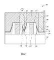
- FIG. 7 is a cross-sectional view of a completed pair of transistors having large area, low resistance source/drain contacts according to one exemplary embodiment described herein.
- references throughout the specification to conventional thin film deposition techniques for depositing silicon nitride, silicon dioxide, metals, or similar materials include such processes as chemical vapor deposition (CVD), low-pressure chemical vapor deposition (LPCVD), metal organic chemical vapor deposition (MOCVD), plasma-enhanced chemical vapor deposition (PECVD), plasma vapor deposition (PVD), atomic layer deposition (ALD), molecular beam epitaxy (MBE), electroplating, electro-less plating, and the like.
- CVD chemical vapor deposition
- LPCVD low-pressure chemical vapor deposition
- MOCVD metal organic chemical vapor deposition
- PECVD plasma-enhanced chemical vapor deposition
- PVD plasma vapor deposition
- ALD atomic layer deposition
- MBE molecular beam epitaxy
- electroplating electro-less plating, and the like.
- a description that references CVD may alternatively be done using PVD, or a description that specifies electroplating may alternatively be accomplished using electro-less plating.
- reference to conventional techniques of thin film formation may include growing a film in-situ.
- controlled growth of an oxide to a desired thickness can be achieved by exposing a silicon surface to oxygen gas or to moisture in a heated chamber.
- photoresist can also be used to pattern a hard mask (e.g., a silicon nitride hard mask), which, in turn, can be used to pattern an underlying film.
- a hard mask e.g., a silicon nitride hard mask
- etching techniques known in the art of semiconductor fabrication for selective removal of polysilicon, silicon nitride, silicon dioxide, metals, photoresist, polyimide, or similar materials includes such processes as wet chemical etching, reactive ion (plasma) etching (RIE), washing, wet cleaning, pre-cleaning, spray cleaning, chemical-mechanical planarization (CMP) and the like. Specific embodiments are described herein with reference to examples of such processes. However, the present disclosure and the reference to certain deposition techniques should not be limited to those described. In some instances, two such techniques may be interchangeable. For example, stripping photoresist may entail immersing a sample in a wet chemical bath or, alternatively, spraying wet chemicals directly onto the sample.
- RIE reactive ion
- CMP chemical-mechanical planarization
- FIG. 1 shows a pair of conventional transistor gate structures 100 formed on a silicon substrate 102 . Two such gate structures are shown.
- the transistor gate structures 100 may be parts of a FinFET transistor array, or an FD-SOI type transistor array, for example.
- Each gate structure 100 includes a metal gate 104 and, adjacent to the metal gate 104 , is a dielectric layer 106 made of silicon nitride (SiN).
- the dielectric layer 106 includes sidewall spacer portions 105 that protect sidewall surfaces of the metal gate 104 , and a dielectric cap portion 107 that protects a top surface of the metal gate 104 .
- a thick insulator 108 covers the gate structures 100 .
- Raised source and drain regions located on either side of each gate structure 100 are formed in an epitaxial layer 110 made of, for example, silicon (Si) or silicon germanium (SiGe).
- the source/drain region 112 located between two adjacent transistors includes a source region for one transistor and a drain region for the other transistor.
- the metal gate 104 is configured to control current flow within the channel region, between the source and the drain.
- the epitaxial layer 110 may form a fin of a FinFET, wherein a portion of the fin serves as the channel region of the FinFET.
- the source and drain regions in the epitaxial layer of the FinFET may extend above the substrate to form a raised source/drain.
- a contact opening 115 is formed by etching away the thick insulator 108 down to the source/drain region 112 .
- the etching step tends to erode the dielectric layer 106 , causing dielectric damage 116 . Erosion of the dielectric layer 106 occurs at a corner of the gate, thus affecting both the sidewall spacer portions 105 and the dielectric cap portion 107 .
- Increasing the thickness of the dielectric layer 106 is not a preferred solution for avoiding the dielectric damage 116 , due to consequences for later processing steps.
- FIGS. 2A and 2B show a comparison of two transistor geometries—a large source/drain region having a wide spacing 122 between adjacent gate structures 100 shown in FIG. 2A , and a scaled down source/drain region having a narrow spacing 124 between adjacent gate structures 100 shown in FIG. 2B .
- the top surface of the epitaxial layer 110 will later support a wide silicide layer 120 , and a narrow silicide layer 126 , respectively, to serve as landing areas for source/drain contacts.
- the spacings 122 , 124 define widths of the respective silicide layers 120 , 126 , which will later determine the contact resistance to the source and drain terminals located between the two gate structures 100 .
- the contact resistance R generally increases linearly with a decrease in the silicide area A.
- FIG. 3 shows a sequence of steps in an inventive method 130 of fabricating large area contacts to the scaled down source/drain region 118 , according to one embodiment. Steps in the method 130 are detailed below with reference to FIGS. 4A, 4B, 5A, 5B, 6A, 6B, and 7 . It is noted that elements of the inventive structures shown in FIGS. 4A-7 that may be similar to corresponding elements of conventional structures shown in the above prior art drawings share the same reference numerals.
- FIG. 4A shows polysilicon dummy gate structures 150 and an epitaxial layer 110 formed on the substrate 102 , according to one embodiment.
- the epitaxial layer 110 is an epitaxial silicon fin of a FinFET.
- dummy gate structures 150 are formed on the substrate 102 according to conventional methods well known in the art of semiconductor device fabrication.
- the substrate 102 can be made of silicon, or the substrate 102 can be a silicon-on-insulator (SOI) substrate that includes a buried oxide layer.
- Each dummy gate structure includes a temporary polysilicon gate 103 , dielectric layer 106 e.g., a conformal silicon nitride (SiN) spacer, and a thick interlayer dielectric (ILD) layer.
- the polysilicon gate 103 is initially formed as an amorphous silicon gate, and then annealed to form a polycrystalline structure.
- the conformal silicon nitride spacer covers the top and the sides of the polysilicon gate 103 .
- the dummy gate structures 150 serve as sacrificial layers that provide a temporary structure during formation of other parts of the FinFETs.
- a thick epitaxial layer 110 is grown from the silicon substrate, between and outside the gate structures 150 .
- the epitaxial layer 110 desirably has a height 151 in the range of about 40-65 nm.
- the epitaxial layer 110 will form source and drain regions and the fin that serves as the channel of the FinFET.
- a thick insulator 108 is formed by depositing a 50-100 nm thick ILD layer such as silicon dioxide (SiO 2 ) on top of the epitaxial layer 110 .
- FIG. 4B shows metal gate structures 152 formed on the substrate 102 , according to one embodiment.
- the metal gate structures 152 serve as gate electrodes configured to control current flow within a channel region of the device.
- the dummy polysilicon gates 103 are replaced with metal gates 104 .
- top portions of the thick insulator 108 and the dielectric layer 106 are removed by chemical-mechanical planarization (CMP). Removal continues down to a top surface of the polysilicon gate 103 , which serves as a polish stop layer, approximately 90 nm above the surface of the substrate 102 .
- CMP chemical-mechanical planarization
- the CMP process thus exposes the polysilicon gates 103 and creates sidewall spacers 158 .
- the polysilicon gates 103 are removed, for example, using a reactive ion etch (RIE) process followed by a wet chemical etch process that consumes silicon with high selectivity to SiN and SiO 2 .
- RIE reactive ion etch
- a high-k insulating material is conformally deposited to form a thin gate oxide, e.g., HfO 2 , followed by deposition of a metal gate that can include, for example, titanium nitride (TiN), titanium carbide (TiC), and tungsten (W).
- a metal gate that can include, for example, titanium nitride (TiN), titanium carbide (TiC), and tungsten (W).
- a tungsten polish step planarizes the metal gates 104 using the sidewall spacers 158 as a CMP stop layer.
- FIGS. 5A-5B show formation of recessed metal gate structures 160 having a dielectric cap 166 , according to one embodiment.
- the metal gates 104 are recessed using a shallow tungsten recess etch process that consumes about 20-30 nm of W with high selectivity to SiN and SiO 2 .
- the dielectric cap layer 162 is formed on top of the recessed metal gate structures 160 .
- the dielectric cap layer 162 can be made of an oxide, nitride, or similar insulating material.
- the dielectric cap layer is then planarized using the sidewall spacers 158 as a CMP stop layer, leaving dielectric caps 166 in the recessed areas over the metal gates 104 .
- FIGS. 6A-6B show formation of V-shaped recessed source and drain regions in the epitaxial layer 100 , according to one embodiment.
- the epitaxial layer 110 is recessed to form V-shaped surface features 172 so as to increase the surface area of the epitaxial layer 110 .
- the source and drain regions are exposed by removing the remainder of the thick insulator 108 using an oxide deglaze process.
- the oxide de-glaze process can be, for example, a hydrofluoric acid (HF) dip.
- the V-shaped surface features 172 will provide the desired sloped bottom profiles for contacts to the source and drain regions.
- the V-shaped epitaxial recess profile can be achieved using a silicon reactive ion etch (RIE) process, e.g., an HBr/O 2 -based plasma etch that is tuned to have a high selectivity to SiN and SiO 2 to prevent erosion of the sidewall spacers 158 and the dielectric caps 166 .
- RIE silicon reactive ion etch
- the etch process chemistry and parameters, e.g., gas pressure, power, and the like, that are used to recess the epitaxial layer 110 can be designed to remove silicon preferentially in a diagonal direction aligned with a certain crystal plane, e.g., the (111) crystal plane, as opposed to the (100) crystal plane which is aligned along the vertical direction.
- V-shaped or crescent-shaped surface features In this way, it is possible to create steeply-sloped sidewalls that form V-shaped or crescent-shaped surface features.
- the depth of the V-shaped surface features 172 is about 25-30 nm.
- the same etch process may result in a U-shaped profile instead of a V-shaped profile.
- a thin metal layer is conformally deposited on top of the metal gate structures and the recessed epitaxial layer 110 .
- a blanket silicide 176 is formed, having a thickness in the range of about 5-10 nm.
- the metal component of the blanket silicide 176 can be any suitable interconnect metal known in the art, e.g., titanium, tungsten, nickel, platinum, and the like.
- the blanket silicide 176 follows the V-shaped surface features 172 .
- a thin hard mask for use as an etch stop liner 179 is formed on the surface of the silicide 176 and the metal gate structures.
- the thin etch stop liner 179 can be, for example, a layer of halfnium oxide (HfO 2 ) having a thickness in the range of about 1-10 nm, with a thickness target of about 3 nm.
- the insulator 108 a thick oxide, is restored on top of the metal gate structures and the V-shaped surface features 172 .
- the insulator 108 then is planarized to a final thickness of at least 100 nm.
- FIG. 7 shows a completed transistor structure 180 having fully formed large surface area contacts 182 , 184 to the source and drain regions, according to one embodiment.
- the large surface area contacts 182 , 184 are vertical columns containing a conducting material, e.g., metal, having a planar top surface, a bottom surface that can have either a planar bottom profile 183 or a sloped bottom profile 185 , and sidewalls 187 that taper from the top surface to the bottom surface.
- the finished contacts shown in FIG. 7 are formed as follows:
- the thick insulator 108 is patterned with self-aligned contacts to form tapered source/drain contact openings.
- the thick oxide can be etched using a chlorine-based RIE process that is selective to the etch stop liner 179 .
- the etch stop liner 179 remains on the corners of the sidewall spacers 158 as a protective layer.
- the etch stop liner 179 also remains on the dielectric cap 166 as an additional mask that prevents erosion of the dielectric cap 166 during the contact etch step.
- the etch stop liner 179 is removed from the silicide 178 at the bottoms of the contact openings using a wet chemical dip.
- the contact openings are filled with metal to form the large surface area contacts 182 , 184 .
- the contact metal can be any suitable metal that is typically used in interconnects such as for example, tungsten, copper, silver, aluminum, titanium, titanium nitride, platinum, and the like, and combinations thereof.
- the contact is lined with TiN and then filled with tungsten (W).
- Contacts 182 that land on relatively open areas of the epitaxial layer 174 can have planar bottom profiles 183 .
- a contact 184 that lands close to a gate or between adjacent transistor gates desirably has a bottom profile 185 that includes one or more substantially sloped portions at the metal-silicide interface.
- the sloped portions can be V-shaped as shown.
- the sloped portions can be U-shaped, crescent-shaped, convex-shaped (conforming to a concave-shaped source/drain region), or they can have any other suitable profile, e.g., wavy, sawtooth, or the like that provides an increased contact area.
Landscapes
- Electrodes Of Semiconductors (AREA)
- Insulated Gate Type Field-Effect Transistor (AREA)
Abstract
Description
Claims (16)
Priority Applications (2)
| Application Number | Priority Date | Filing Date | Title |
|---|---|---|---|
| US14/584,639 US9466722B2 (en) | 2014-12-29 | 2014-12-29 | Large area contacts for small transistors |
| US15/273,778 US10749031B2 (en) | 2014-12-29 | 2016-09-23 | Large area contacts for small transistors |
Applications Claiming Priority (1)
| Application Number | Priority Date | Filing Date | Title |
|---|---|---|---|
| US14/584,639 US9466722B2 (en) | 2014-12-29 | 2014-12-29 | Large area contacts for small transistors |
Related Child Applications (1)
| Application Number | Title | Priority Date | Filing Date |
|---|---|---|---|
| US15/273,778 Continuation US10749031B2 (en) | 2014-12-29 | 2016-09-23 | Large area contacts for small transistors |
Publications (2)
| Publication Number | Publication Date |
|---|---|
| US20160190322A1 US20160190322A1 (en) | 2016-06-30 |
| US9466722B2 true US9466722B2 (en) | 2016-10-11 |
Family
ID=56165201
Family Applications (2)
| Application Number | Title | Priority Date | Filing Date |
|---|---|---|---|
| US14/584,639 Active US9466722B2 (en) | 2014-12-29 | 2014-12-29 | Large area contacts for small transistors |
| US15/273,778 Expired - Fee Related US10749031B2 (en) | 2014-12-29 | 2016-09-23 | Large area contacts for small transistors |
Family Applications After (1)
| Application Number | Title | Priority Date | Filing Date |
|---|---|---|---|
| US15/273,778 Expired - Fee Related US10749031B2 (en) | 2014-12-29 | 2016-09-23 | Large area contacts for small transistors |
Country Status (1)
| Country | Link |
|---|---|
| US (2) | US9466722B2 (en) |
Cited By (7)
| Publication number | Priority date | Publication date | Assignee | Title |
|---|---|---|---|---|
| US9755057B1 (en) * | 2016-07-28 | 2017-09-05 | United Microelectronics Corp. | Method of fabricating a semiconductor device |
| US20170278942A1 (en) * | 2014-08-01 | 2017-09-28 | International Business Machines Corporation | Extended contact area using undercut silicide extensions |
| US10312139B2 (en) * | 2015-06-26 | 2019-06-04 | Taiwan Semiconductor Manufacturing Company, Ltd. | Interconnect structure having an etch stop layer over conductive lines |
| US10388745B1 (en) * | 2018-03-22 | 2019-08-20 | Varian Semiconductor Equipment Associates, Inc. | Structure and method of forming transistor device having improved gate contact arrangement |
| US10403547B2 (en) * | 2017-12-12 | 2019-09-03 | Varian Semiconductor Equipment Associates, Inc. | Structure and method of forming self aligned contacts in semiconductor device |
| US10522423B2 (en) | 2017-08-30 | 2019-12-31 | Taiwan Semiconductor Manufacturing Co., Ltd. | Interconnect structure for fin-like field effect transistor |
| US11935931B2 (en) | 2020-06-06 | 2024-03-19 | International Business Machines Corporation | Selective shrink for contact trench |
Families Citing this family (13)
| Publication number | Priority date | Publication date | Assignee | Title |
|---|---|---|---|---|
| CN109196652A (en) * | 2016-07-02 | 2019-01-11 | 英特尔公司 | III-V FINFET transistors with V-groove S/D profile for improved access resistance |
| WO2018063207A1 (en) * | 2016-09-29 | 2018-04-05 | Intel Corporation | Resistive random access memory cell |
| EP3339244A1 (en) * | 2016-12-21 | 2018-06-27 | IMEC vzw | Source and drain contacts in fin- or nanowire- based semiconductor devices. |
| CN108878528B (en) * | 2017-05-16 | 2021-08-06 | 中芯国际集成电路制造(上海)有限公司 | Semiconductor structure and method of forming the same |
| US10522392B2 (en) * | 2017-05-31 | 2019-12-31 | Taiwan Semiconductor Manufacturing Co., Ltd. | Semiconductor device and method of fabricating the same |
| WO2019066789A1 (en) * | 2017-09-27 | 2019-04-04 | Intel Corporation | Epitaxial iii-n nanoribbon structures for device fabrication |
| CN109599337A (en) * | 2017-09-30 | 2019-04-09 | 中芯国际集成电路制造(上海)有限公司 | Semiconductor devices and forming method thereof |
| US10553492B2 (en) * | 2018-04-30 | 2020-02-04 | Taiwan Semiconductor Manufacturing Company, Ltd. | Selective NFET/PFET recess of source/drain regions |
| US10868118B2 (en) * | 2018-08-31 | 2020-12-15 | Taiwan Semiconductor Manufacturing Co., Ltd. | Methods of forming epitaxial source/drain features in semiconductor devices |
| US11195753B2 (en) * | 2018-09-18 | 2021-12-07 | International Business Machines Corporation | Tiered-profile contact for semiconductor |
| US10818548B1 (en) * | 2019-05-30 | 2020-10-27 | International Business Machines Corporation | Method and structure for cost effective enhanced self-aligned contacts |
| US11264419B2 (en) * | 2019-12-30 | 2022-03-01 | Omnivision Technologies, Inc. | Image sensor with fully depleted silicon on insulator substrate |
| US20240096806A1 (en) * | 2022-09-21 | 2024-03-21 | Taiwan Semiconductor Manufacturing Company Ltd. | Semiconductor structure and method of manufacturing the same |
Citations (9)
| Publication number | Priority date | Publication date | Assignee | Title |
|---|---|---|---|---|
| US20040262650A1 (en) | 2000-01-07 | 2004-12-30 | Sharp Kabushiki Kaisha | Semiconductor device, method for producing the same, and information processing apparatus |
| US20130065371A1 (en) * | 2011-09-13 | 2013-03-14 | Globalfoundries Inc. | Methods for fabricating integrated circuits |
| US20140001561A1 (en) | 2012-06-27 | 2014-01-02 | International Business Machines Corporation | Cmos devices having strain source/drain regions and low contact resistance |
| US20140054715A1 (en) | 2012-08-21 | 2014-02-27 | Stmicroelectronics, Inc. | Semiconductor device with an inclined source/drain and associated methods |
| US20140264348A1 (en) * | 2013-03-13 | 2014-09-18 | Taiwan Semiconductor Manufacturing Co, Ltd. | Asymmetric Cyclic Desposition Etch Epitaxy |
| US20140361352A1 (en) * | 2013-06-06 | 2014-12-11 | United Microelectronics Corp. | Semiconductor device and fabrication method thereof |
| US20140363984A1 (en) * | 2013-06-10 | 2014-12-11 | Fujitsu Semiconductor Limited | Manufacturing method of semiconductor device |
| US8946828B2 (en) * | 2010-02-09 | 2015-02-03 | Taiwan Semiconductor Manufacturing Company, Ltd. | Semiconductor device having elevated structure and method of manufacturing the same |
| US9331159B1 (en) * | 2015-02-06 | 2016-05-03 | Globalfoundries Inc. | Fabricating transistor(s) with raised active regions having angled upper surfaces |
-
2014
- 2014-12-29 US US14/584,639 patent/US9466722B2/en active Active
-
2016
- 2016-09-23 US US15/273,778 patent/US10749031B2/en not_active Expired - Fee Related
Patent Citations (10)
| Publication number | Priority date | Publication date | Assignee | Title |
|---|---|---|---|---|
| US20040262650A1 (en) | 2000-01-07 | 2004-12-30 | Sharp Kabushiki Kaisha | Semiconductor device, method for producing the same, and information processing apparatus |
| US8946828B2 (en) * | 2010-02-09 | 2015-02-03 | Taiwan Semiconductor Manufacturing Company, Ltd. | Semiconductor device having elevated structure and method of manufacturing the same |
| US20130065371A1 (en) * | 2011-09-13 | 2013-03-14 | Globalfoundries Inc. | Methods for fabricating integrated circuits |
| US20140001561A1 (en) | 2012-06-27 | 2014-01-02 | International Business Machines Corporation | Cmos devices having strain source/drain regions and low contact resistance |
| US20140054715A1 (en) | 2012-08-21 | 2014-02-27 | Stmicroelectronics, Inc. | Semiconductor device with an inclined source/drain and associated methods |
| US9012999B2 (en) * | 2012-08-21 | 2015-04-21 | Stmicroelectronics, Inc. | Semiconductor device with an inclined source/drain and associated methods |
| US20140264348A1 (en) * | 2013-03-13 | 2014-09-18 | Taiwan Semiconductor Manufacturing Co, Ltd. | Asymmetric Cyclic Desposition Etch Epitaxy |
| US20140361352A1 (en) * | 2013-06-06 | 2014-12-11 | United Microelectronics Corp. | Semiconductor device and fabrication method thereof |
| US20140363984A1 (en) * | 2013-06-10 | 2014-12-11 | Fujitsu Semiconductor Limited | Manufacturing method of semiconductor device |
| US9331159B1 (en) * | 2015-02-06 | 2016-05-03 | Globalfoundries Inc. | Fabricating transistor(s) with raised active regions having angled upper surfaces |
Cited By (11)
| Publication number | Priority date | Publication date | Assignee | Title |
|---|---|---|---|---|
| US20170278942A1 (en) * | 2014-08-01 | 2017-09-28 | International Business Machines Corporation | Extended contact area using undercut silicide extensions |
| US10347739B2 (en) * | 2014-08-01 | 2019-07-09 | International Business Machines Corporation | Extended contact area using undercut silicide extensions |
| US10312139B2 (en) * | 2015-06-26 | 2019-06-04 | Taiwan Semiconductor Manufacturing Company, Ltd. | Interconnect structure having an etch stop layer over conductive lines |
| US10861742B2 (en) | 2015-06-26 | 2020-12-08 | Taiwan Semiconductor Manufacturing Company, Ltd. | Interconnect structure having an etch stop layer over conductive lines |
| US11569124B2 (en) | 2015-06-26 | 2023-01-31 | Taiwan Semiconductor Manufacturing Company, Ltd. | Interconnect structure having an etch stop layer over conductive lines |
| US9755057B1 (en) * | 2016-07-28 | 2017-09-05 | United Microelectronics Corp. | Method of fabricating a semiconductor device |
| US10177245B2 (en) | 2016-07-28 | 2019-01-08 | United Microelectronics Corp. | Method of fabricating a semiconductor device |
| US10522423B2 (en) | 2017-08-30 | 2019-12-31 | Taiwan Semiconductor Manufacturing Co., Ltd. | Interconnect structure for fin-like field effect transistor |
| US10403547B2 (en) * | 2017-12-12 | 2019-09-03 | Varian Semiconductor Equipment Associates, Inc. | Structure and method of forming self aligned contacts in semiconductor device |
| US10388745B1 (en) * | 2018-03-22 | 2019-08-20 | Varian Semiconductor Equipment Associates, Inc. | Structure and method of forming transistor device having improved gate contact arrangement |
| US11935931B2 (en) | 2020-06-06 | 2024-03-19 | International Business Machines Corporation | Selective shrink for contact trench |
Also Published As
| Publication number | Publication date |
|---|---|
| US20160190322A1 (en) | 2016-06-30 |
| US10749031B2 (en) | 2020-08-18 |
| US20170012130A1 (en) | 2017-01-12 |
Similar Documents
| Publication | Publication Date | Title |
|---|---|---|
| US9466722B2 (en) | Large area contacts for small transistors | |
| US9685555B2 (en) | High-reliability, low-resistance contacts for nanoscale transistors | |
| US8586455B1 (en) | Preventing shorting of adjacent devices | |
| US9502518B2 (en) | Multi-channel gate-all-around FET | |
| US7935598B2 (en) | Vertical channel transistor and method of fabricating the same | |
| US9673100B2 (en) | Semiconductor device having contact plug in two dielectric layers and two etch stop layers | |
| US10886386B2 (en) | Dual width FinFET | |
| US10326000B2 (en) | FinFET with reduced parasitic capacitance | |
| US20160293715A1 (en) | Semiconductor structure having source/drain gouging immunity | |
| US20200321252A1 (en) | Geometry for Threshold Voltage Tuning on Semiconductor Device | |
| US20200312849A1 (en) | Gate recess uniformity in vertical field effect transistor | |
| US10665590B2 (en) | Wrap-around contact surrounding epitaxial regions of integrated circuit structures and method of forming same | |
| US10115724B1 (en) | Double diffusion break gate structure without vestigial antenna capacitance | |
| KR102849318B1 (en) | Semiconductor device and method | |
| US8927406B2 (en) | Dual damascene metal gate | |
| US10008409B2 (en) | Method for fabricating a semiconductor device | |
| US9748349B2 (en) | Semiconductor device | |
| US10438955B2 (en) | Devices with contact-to-gate shorting through conductive paths between fins and fabrication methods | |
| US20150325695A1 (en) | Semiconductor apparatus, method for fabricating the same, and variable resistive memory device | |
| US20150129939A1 (en) | Method and structure for forming contacts | |
| US20170047251A1 (en) | Method of manufacturing a semiconductor device including forming a dielectric layer around a patterned etch mask | |
| US20260107557A1 (en) | Selective gate electrode layer desposition in stacking transistors and structures resulting therefrom | |
| US20140264553A1 (en) | Method of fabricating monos semiconductor device |
Legal Events
| Date | Code | Title | Description |
|---|---|---|---|
| AS | Assignment |
Owner name: GLOBALFOUNDRIES INC., CAYMAN ISLANDS Free format text: ASSIGNMENT OF ASSIGNORS INTEREST;ASSIGNORS:XIE, RUILONG;CAI, XIUYU;SIGNING DATES FROM 20141219 TO 20141222;REEL/FRAME:034603/0828 Owner name: STMICROELECTRONICS, INC., TEXAS Free format text: ASSIGNMENT OF ASSIGNORS INTEREST;ASSIGNOR:LIU, QING;REEL/FRAME:034603/0817 Effective date: 20141218 Owner name: INTERNATIONAL BUSINESS MACHINES CORPORATION, NEW Y Free format text: ASSIGNMENT OF ASSIGNORS INTEREST;ASSIGNOR:YEH, CHUN-CHEN;REEL/FRAME:034603/0831 Effective date: 20141219 |
|
| STCF | Information on status: patent grant |
Free format text: PATENTED CASE |
|
| CC | Certificate of correction | ||
| AS | Assignment |
Owner name: WILMINGTON TRUST, NATIONAL ASSOCIATION, DELAWARE Free format text: SECURITY AGREEMENT;ASSIGNOR:GLOBALFOUNDRIES INC.;REEL/FRAME:049490/0001 Effective date: 20181127 |
|
| MAFP | Maintenance fee payment |
Free format text: PAYMENT OF MAINTENANCE FEE, 4TH YEAR, LARGE ENTITY (ORIGINAL EVENT CODE: M1551); ENTITY STATUS OF PATENT OWNER: LARGE ENTITY Year of fee payment: 4 |
|
| AS | Assignment |
Owner name: GLOBALFOUNDRIES U.S. INC., CALIFORNIA Free format text: ASSIGNMENT OF ASSIGNORS INTEREST;ASSIGNOR:GLOBALFOUNDRIES INC.;REEL/FRAME:054633/0001 Effective date: 20201022 |
|
| AS | Assignment |
Owner name: GLOBALFOUNDRIES INC., CAYMAN ISLANDS Free format text: RELEASE BY SECURED PARTY;ASSIGNOR:WILMINGTON TRUST, NATIONAL ASSOCIATION;REEL/FRAME:054636/0001 Effective date: 20201117 |
|
| AS | Assignment |
Owner name: GLOBALFOUNDRIES U.S. INC., NEW YORK Free format text: RELEASE BY SECURED PARTY;ASSIGNOR:WILMINGTON TRUST, NATIONAL ASSOCIATION;REEL/FRAME:056987/0001 Effective date: 20201117 Owner name: GLOBALFOUNDRIES U.S. INC., NEW YORK Free format text: RELEASE OF SECURITY INTEREST;ASSIGNOR:WILMINGTON TRUST, NATIONAL ASSOCIATION;REEL/FRAME:056987/0001 Effective date: 20201117 |
|
| MAFP | Maintenance fee payment |
Free format text: PAYMENT OF MAINTENANCE FEE, 8TH YEAR, LARGE ENTITY (ORIGINAL EVENT CODE: M1552); ENTITY STATUS OF PATENT OWNER: LARGE ENTITY Year of fee payment: 8 |