US9466620B2 - Method for manufacturing array substrate, array substrate, and display device - Google Patents
Method for manufacturing array substrate, array substrate, and display device Download PDFInfo
- Publication number
- US9466620B2 US9466620B2 US14/488,029 US201414488029A US9466620B2 US 9466620 B2 US9466620 B2 US 9466620B2 US 201414488029 A US201414488029 A US 201414488029A US 9466620 B2 US9466620 B2 US 9466620B2
- Authority
- US
- United States
- Prior art keywords
- electrode
- layer
- gate
- insulating layer
- source
- Prior art date
- Legal status (The legal status is an assumption and is not a legal conclusion. Google has not performed a legal analysis and makes no representation as to the accuracy of the status listed.)
- Expired - Fee Related
Links
Images


Classifications
-
- H—ELECTRICITY
- H10—SEMICONDUCTOR DEVICES; ELECTRIC SOLID-STATE DEVICES NOT OTHERWISE PROVIDED FOR
- H10D—INORGANIC ELECTRIC SEMICONDUCTOR DEVICES
- H10D64/00—Electrodes of devices having potential barriers
- H10D64/20—Electrodes characterised by their shapes, relative sizes or dispositions
- H10D64/27—Electrodes not carrying the current to be rectified, amplified, oscillated or switched, e.g. gates
- H10D64/311—Gate electrodes for field-effect devices
- H10D64/411—Gate electrodes for field-effect devices for FETs
- H10D64/511—Gate electrodes for field-effect devices for FETs for IGFETs
- H10D64/514—Gate electrodes for field-effect devices for FETs for IGFETs characterised by the insulating layers
-
- H01L27/1237—
-
- G—PHYSICS
- G02—OPTICS
- G02F—OPTICAL DEVICES OR ARRANGEMENTS FOR THE CONTROL OF LIGHT BY MODIFICATION OF THE OPTICAL PROPERTIES OF THE MEDIA OF THE ELEMENTS INVOLVED THEREIN; NON-LINEAR OPTICS; FREQUENCY-CHANGING OF LIGHT; OPTICAL LOGIC ELEMENTS; OPTICAL ANALOGUE/DIGITAL CONVERTERS
- G02F1/00—Devices or arrangements for the control of the intensity, colour, phase, polarisation or direction of light arriving from an independent light source, e.g. switching, gating or modulating; Non-linear optics
- G02F1/01—Devices or arrangements for the control of the intensity, colour, phase, polarisation or direction of light arriving from an independent light source, e.g. switching, gating or modulating; Non-linear optics for the control of the intensity, phase, polarisation or colour
- G02F1/13—Devices or arrangements for the control of the intensity, colour, phase, polarisation or direction of light arriving from an independent light source, e.g. switching, gating or modulating; Non-linear optics for the control of the intensity, phase, polarisation or colour based on liquid crystals, e.g. single liquid crystal display cells
- G02F1/133—Constructional arrangements; Operation of liquid crystal cells; Circuit arrangements
- G02F1/136—Liquid crystal cells structurally associated with a semi-conducting layer or substrate, e.g. cells forming part of an integrated circuit
- G02F1/1362—Active matrix addressed cells
-
- H01L21/31111—
-
- H01L21/32051—
-
- H01L21/32133—
-
- H01L21/56—
-
- H01L21/76802—
-
- H01L23/3171—
-
- H01L27/127—
-
- H01L29/41733—
-
- H01L29/42384—
-
- H01L29/66765—
-
- H01L29/78684—
-
- H—ELECTRICITY
- H10—SEMICONDUCTOR DEVICES; ELECTRIC SOLID-STATE DEVICES NOT OTHERWISE PROVIDED FOR
- H10D—INORGANIC ELECTRIC SEMICONDUCTOR DEVICES
- H10D30/00—Field-effect transistors [FET]
- H10D30/01—Manufacture or treatment
- H10D30/021—Manufacture or treatment of FETs having insulated gates [IGFET]
- H10D30/031—Manufacture or treatment of FETs having insulated gates [IGFET] of thin-film transistors [TFT]
- H10D30/0312—Manufacture or treatment of FETs having insulated gates [IGFET] of thin-film transistors [TFT] characterised by the gate electrodes
- H10D30/0316—Manufacture or treatment of FETs having insulated gates [IGFET] of thin-film transistors [TFT] characterised by the gate electrodes of lateral bottom-gate TFTs comprising only a single gate
-
- H—ELECTRICITY
- H10—SEMICONDUCTOR DEVICES; ELECTRIC SOLID-STATE DEVICES NOT OTHERWISE PROVIDED FOR
- H10D—INORGANIC ELECTRIC SEMICONDUCTOR DEVICES
- H10D30/00—Field-effect transistors [FET]
- H10D30/01—Manufacture or treatment
- H10D30/021—Manufacture or treatment of FETs having insulated gates [IGFET]
- H10D30/031—Manufacture or treatment of FETs having insulated gates [IGFET] of thin-film transistors [TFT]
- H10D30/0321—Manufacture or treatment of FETs having insulated gates [IGFET] of thin-film transistors [TFT] comprising silicon, e.g. amorphous silicon or polysilicon
-
- H—ELECTRICITY
- H10—SEMICONDUCTOR DEVICES; ELECTRIC SOLID-STATE DEVICES NOT OTHERWISE PROVIDED FOR
- H10D—INORGANIC ELECTRIC SEMICONDUCTOR DEVICES
- H10D30/00—Field-effect transistors [FET]
- H10D30/60—Insulated-gate field-effect transistors [IGFET]
- H10D30/67—Thin-film transistors [TFT]
- H10D30/6729—Thin-film transistors [TFT] characterised by the electrodes
- H10D30/673—Thin-film transistors [TFT] characterised by the electrodes characterised by the shapes, relative sizes or dispositions of the gate electrodes
-
- H—ELECTRICITY
- H10—SEMICONDUCTOR DEVICES; ELECTRIC SOLID-STATE DEVICES NOT OTHERWISE PROVIDED FOR
- H10D—INORGANIC ELECTRIC SEMICONDUCTOR DEVICES
- H10D30/00—Field-effect transistors [FET]
- H10D30/60—Insulated-gate field-effect transistors [IGFET]
- H10D30/67—Thin-film transistors [TFT]
- H10D30/674—Thin-film transistors [TFT] characterised by the active materials
- H10D30/6741—Group IV materials, e.g. germanium or silicon carbide
- H10D30/6743—Silicon
- H10D30/6744—Monocrystalline silicon
-
- H—ELECTRICITY
- H10—SEMICONDUCTOR DEVICES; ELECTRIC SOLID-STATE DEVICES NOT OTHERWISE PROVIDED FOR
- H10D—INORGANIC ELECTRIC SEMICONDUCTOR DEVICES
- H10D84/00—Integrated devices formed in or on semiconductor substrates that comprise only semiconducting layers, e.g. on Si wafers or on GaAs-on-Si wafers
- H10D84/01—Manufacture or treatment
-
- H—ELECTRICITY
- H10—SEMICONDUCTOR DEVICES; ELECTRIC SOLID-STATE DEVICES NOT OTHERWISE PROVIDED FOR
- H10D—INORGANIC ELECTRIC SEMICONDUCTOR DEVICES
- H10D86/00—Integrated devices formed in or on insulating or conducting substrates, e.g. formed in silicon-on-insulator [SOI] substrates or on stainless steel or glass substrates
- H10D86/01—Manufacture or treatment
- H10D86/021—Manufacture or treatment of multiple TFTs
- H10D86/0221—Manufacture or treatment of multiple TFTs comprising manufacture, treatment or patterning of TFT semiconductor bodies
-
- H—ELECTRICITY
- H10—SEMICONDUCTOR DEVICES; ELECTRIC SOLID-STATE DEVICES NOT OTHERWISE PROVIDED FOR
- H10D—INORGANIC ELECTRIC SEMICONDUCTOR DEVICES
- H10D86/00—Integrated devices formed in or on insulating or conducting substrates, e.g. formed in silicon-on-insulator [SOI] substrates or on stainless steel or glass substrates
- H10D86/01—Manufacture or treatment
- H10D86/021—Manufacture or treatment of multiple TFTs
- H10D86/0231—Manufacture or treatment of multiple TFTs using masks, e.g. half-tone masks
-
- H—ELECTRICITY
- H10—SEMICONDUCTOR DEVICES; ELECTRIC SOLID-STATE DEVICES NOT OTHERWISE PROVIDED FOR
- H10D—INORGANIC ELECTRIC SEMICONDUCTOR DEVICES
- H10D86/00—Integrated devices formed in or on insulating or conducting substrates, e.g. formed in silicon-on-insulator [SOI] substrates or on stainless steel or glass substrates
- H10D86/40—Integrated devices formed in or on insulating or conducting substrates, e.g. formed in silicon-on-insulator [SOI] substrates or on stainless steel or glass substrates characterised by multiple TFTs
- H10D86/431—Integrated devices formed in or on insulating or conducting substrates, e.g. formed in silicon-on-insulator [SOI] substrates or on stainless steel or glass substrates characterised by multiple TFTs having different compositions, shapes, layouts or thicknesses of gate insulators in different TFTs
-
- H—ELECTRICITY
- H10—SEMICONDUCTOR DEVICES; ELECTRIC SOLID-STATE DEVICES NOT OTHERWISE PROVIDED FOR
- H10D—INORGANIC ELECTRIC SEMICONDUCTOR DEVICES
- H10D86/00—Integrated devices formed in or on insulating or conducting substrates, e.g. formed in silicon-on-insulator [SOI] substrates or on stainless steel or glass substrates
- H10D86/40—Integrated devices formed in or on insulating or conducting substrates, e.g. formed in silicon-on-insulator [SOI] substrates or on stainless steel or glass substrates characterised by multiple TFTs
- H10D86/441—Interconnections, e.g. scanning lines
-
- H—ELECTRICITY
- H10—SEMICONDUCTOR DEVICES; ELECTRIC SOLID-STATE DEVICES NOT OTHERWISE PROVIDED FOR
- H10D—INORGANIC ELECTRIC SEMICONDUCTOR DEVICES
- H10D86/00—Integrated devices formed in or on insulating or conducting substrates, e.g. formed in silicon-on-insulator [SOI] substrates or on stainless steel or glass substrates
- H10D86/40—Integrated devices formed in or on insulating or conducting substrates, e.g. formed in silicon-on-insulator [SOI] substrates or on stainless steel or glass substrates characterised by multiple TFTs
- H10D86/451—Integrated devices formed in or on insulating or conducting substrates, e.g. formed in silicon-on-insulator [SOI] substrates or on stainless steel or glass substrates characterised by multiple TFTs characterised by the compositions or shapes of the interlayer dielectrics
-
- H—ELECTRICITY
- H10—SEMICONDUCTOR DEVICES; ELECTRIC SOLID-STATE DEVICES NOT OTHERWISE PROVIDED FOR
- H10D—INORGANIC ELECTRIC SEMICONDUCTOR DEVICES
- H10D86/00—Integrated devices formed in or on insulating or conducting substrates, e.g. formed in silicon-on-insulator [SOI] substrates or on stainless steel or glass substrates
- H10D86/40—Integrated devices formed in or on insulating or conducting substrates, e.g. formed in silicon-on-insulator [SOI] substrates or on stainless steel or glass substrates characterised by multiple TFTs
- H10D86/60—Integrated devices formed in or on insulating or conducting substrates, e.g. formed in silicon-on-insulator [SOI] substrates or on stainless steel or glass substrates characterised by multiple TFTs wherein the TFTs are in active matrices
-
- H—ELECTRICITY
- H10—SEMICONDUCTOR DEVICES; ELECTRIC SOLID-STATE DEVICES NOT OTHERWISE PROVIDED FOR
- H10D—INORGANIC ELECTRIC SEMICONDUCTOR DEVICES
- H10D89/00—Aspects of integrated devices not covered by groups H10D84/00 - H10D88/00
-
- H—ELECTRICITY
- H10—SEMICONDUCTOR DEVICES; ELECTRIC SOLID-STATE DEVICES NOT OTHERWISE PROVIDED FOR
- H10P—GENERIC PROCESSES OR APPARATUS FOR THE MANUFACTURE OR TREATMENT OF DEVICES COVERED BY CLASS H10
- H10P14/00—Formation of materials, e.g. in the shape of layers or pillars
- H10P14/40—Formation of materials, e.g. in the shape of layers or pillars of conductive or resistive materials
- H10P14/412—Deposition of metallic or metal-silicide materials
-
- H—ELECTRICITY
- H10—SEMICONDUCTOR DEVICES; ELECTRIC SOLID-STATE DEVICES NOT OTHERWISE PROVIDED FOR
- H10P—GENERIC PROCESSES OR APPARATUS FOR THE MANUFACTURE OR TREATMENT OF DEVICES COVERED BY CLASS H10
- H10P50/00—Etching of wafers, substrates or parts of devices
- H10P50/20—Dry etching; Plasma etching; Reactive-ion etching
- H10P50/26—Dry etching; Plasma etching; Reactive-ion etching of conductive or resistive materials
- H10P50/264—Dry etching; Plasma etching; Reactive-ion etching of conductive or resistive materials by chemical means
-
- H—ELECTRICITY
- H10—SEMICONDUCTOR DEVICES; ELECTRIC SOLID-STATE DEVICES NOT OTHERWISE PROVIDED FOR
- H10P—GENERIC PROCESSES OR APPARATUS FOR THE MANUFACTURE OR TREATMENT OF DEVICES COVERED BY CLASS H10
- H10P50/00—Etching of wafers, substrates or parts of devices
- H10P50/20—Dry etching; Plasma etching; Reactive-ion etching
- H10P50/28—Dry etching; Plasma etching; Reactive-ion etching of insulating materials
- H10P50/282—Dry etching; Plasma etching; Reactive-ion etching of insulating materials of inorganic materials
- H10P50/283—Dry etching; Plasma etching; Reactive-ion etching of insulating materials of inorganic materials by chemical means
-
- H—ELECTRICITY
- H10—SEMICONDUCTOR DEVICES; ELECTRIC SOLID-STATE DEVICES NOT OTHERWISE PROVIDED FOR
- H10W—GENERIC PACKAGES, INTERCONNECTIONS, CONNECTORS OR OTHER CONSTRUCTIONAL DETAILS OF DEVICES COVERED BY CLASS H10
- H10W20/00—Interconnections in chips, wafers or substrates
- H10W20/01—Manufacture or treatment
- H10W20/071—Manufacture or treatment of dielectric parts thereof
- H10W20/081—Manufacture or treatment of dielectric parts thereof by forming openings in the dielectric parts
-
- H—ELECTRICITY
- H10—SEMICONDUCTOR DEVICES; ELECTRIC SOLID-STATE DEVICES NOT OTHERWISE PROVIDED FOR
- H10W—GENERIC PACKAGES, INTERCONNECTIONS, CONNECTORS OR OTHER CONSTRUCTIONAL DETAILS OF DEVICES COVERED BY CLASS H10
- H10W74/00—Encapsulations, e.g. protective coatings
- H10W74/01—Manufacture or treatment
-
- H—ELECTRICITY
- H10—SEMICONDUCTOR DEVICES; ELECTRIC SOLID-STATE DEVICES NOT OTHERWISE PROVIDED FOR
- H10W—GENERIC PACKAGES, INTERCONNECTIONS, CONNECTORS OR OTHER CONSTRUCTIONAL DETAILS OF DEVICES COVERED BY CLASS H10
- H10W74/00—Encapsulations, e.g. protective coatings
- H10W74/10—Encapsulations, e.g. protective coatings characterised by their shape or disposition
- H10W74/131—Encapsulations, e.g. protective coatings characterised by their shape or disposition the semiconductor body being only partially enclosed
- H10W74/137—Encapsulations, e.g. protective coatings characterised by their shape or disposition the semiconductor body being only partially enclosed the encapsulations being directly on the semiconductor body
-
- G—PHYSICS
- G02—OPTICS
- G02F—OPTICAL DEVICES OR ARRANGEMENTS FOR THE CONTROL OF LIGHT BY MODIFICATION OF THE OPTICAL PROPERTIES OF THE MEDIA OF THE ELEMENTS INVOLVED THEREIN; NON-LINEAR OPTICS; FREQUENCY-CHANGING OF LIGHT; OPTICAL LOGIC ELEMENTS; OPTICAL ANALOGUE/DIGITAL CONVERTERS
- G02F1/00—Devices or arrangements for the control of the intensity, colour, phase, polarisation or direction of light arriving from an independent light source, e.g. switching, gating or modulating; Non-linear optics
- G02F1/01—Devices or arrangements for the control of the intensity, colour, phase, polarisation or direction of light arriving from an independent light source, e.g. switching, gating or modulating; Non-linear optics for the control of the intensity, phase, polarisation or colour
- G02F1/13—Devices or arrangements for the control of the intensity, colour, phase, polarisation or direction of light arriving from an independent light source, e.g. switching, gating or modulating; Non-linear optics for the control of the intensity, phase, polarisation or colour based on liquid crystals, e.g. single liquid crystal display cells
- G02F1/133—Constructional arrangements; Operation of liquid crystal cells; Circuit arrangements
- G02F1/136—Liquid crystal cells structurally associated with a semi-conducting layer or substrate, e.g. cells forming part of an integrated circuit
- G02F1/1362—Active matrix addressed cells
- G02F1/136231—Active matrix addressed cells for reducing the number of lithographic steps
- G02F1/136236—Active matrix addressed cells for reducing the number of lithographic steps using a grey or half tone lithographic process
-
- G02F2001/136236—
-
- H01L2924/00—
-
- H01L2924/0002—
-
- H—ELECTRICITY
- H10—SEMICONDUCTOR DEVICES; ELECTRIC SOLID-STATE DEVICES NOT OTHERWISE PROVIDED FOR
- H10D—INORGANIC ELECTRIC SEMICONDUCTOR DEVICES
- H10D30/00—Field-effect transistors [FET]
- H10D30/60—Insulated-gate field-effect transistors [IGFET]
- H10D30/67—Thin-film transistors [TFT]
- H10D30/6729—Thin-film transistors [TFT] characterised by the electrodes
- H10D30/673—Thin-film transistors [TFT] characterised by the electrodes characterised by the shapes, relative sizes or dispositions of the gate electrodes
- H10D30/6736—Thin-film transistors [TFT] characterised by the electrodes characterised by the shapes, relative sizes or dispositions of the gate electrodes characterised by the shape of gate insulators
-
- H—ELECTRICITY
- H10—SEMICONDUCTOR DEVICES; ELECTRIC SOLID-STATE DEVICES NOT OTHERWISE PROVIDED FOR
- H10P—GENERIC PROCESSES OR APPARATUS FOR THE MANUFACTURE OR TREATMENT OF DEVICES COVERED BY CLASS H10
- H10P50/00—Etching of wafers, substrates or parts of devices
- H10P50/73—Etching of wafers, substrates or parts of devices using masks for insulating materials
-
- H—ELECTRICITY
- H10—SEMICONDUCTOR DEVICES; ELECTRIC SOLID-STATE DEVICES NOT OTHERWISE PROVIDED FOR
- H10P—GENERIC PROCESSES OR APPARATUS FOR THE MANUFACTURE OR TREATMENT OF DEVICES COVERED BY CLASS H10
- H10P76/00—Manufacture or treatment of masks on semiconductor bodies, e.g. by lithography or photolithography
- H10P76/20—Manufacture or treatment of masks on semiconductor bodies, e.g. by lithography or photolithography of masks comprising organic materials
- H10P76/204—Manufacture or treatment of masks on semiconductor bodies, e.g. by lithography or photolithography of masks comprising organic materials of organic photoresist masks
- H10P76/2041—Photolithographic processes
Definitions
- the present invention relates to the field of liquid crystal display, in particular to a method for manufacturing an array substrate, the array substrate, and a display device.
- a liquid crystal display mainly comprises a liquid crystal panel, which includes a thin film transistor (TFT) array substrate, a color filter substrate, and liquid crystals arranged therebetween.
- the TFT array substrate is a mainstream one now, and usually it includes a multilayered structure consisting of a gate electrode layer, a gate insulating layer, an active layer, a source/drain electrode layer, an insulation protecting layer, and a pixel electrode layer.
- a layer of a non-metallic material is deposited by plasma-enhanced chemical deposition.
- An important improvement in the liquid crystal display is to enhance an aperture ratio and reduce power consumption.
- In order to enhance the aperture ratio usually two ITO layers and multilayered wiring are arranged on the TFT array substrate.
- the capacitance between source and drain electrodes and a gate electrode will be relatively large, and a load of the TFT will be increased, and as a result, the power consumption of a liquid crystal display screen is very high.
- a battery of an existing mobile phone generally has poor endurance, and it is required to reduce the power consumption.
- An object of the present invention is to provide a method for manufacturing an array substrate with low power consumption, so as to prevent an increase in the load of a TFT and the load of a pixel due to the large capacitance between source and drain electrodes and a gate electrode in the prior art, thereby to reduce the power consumption of the entire display device.
- the present invention provides a method for manufacturing an array substrate with low power consumption, comprising:
- a pattern of a gate electrode by a one-time patterning process, the pattern of the gate electrode covering the partially-etched region of the gate insulating layer and a region of the gate insulating layer corresponding to the source and drain electrodes.
- the pattern of the gate electrode and the active layer are located at different sides of the gate insulating layer, and the gate insulating layer between the source and drain electrodes and the pattern of the gate electrode has a thickness greater than that of the gate insulating layer between the active layer, located between the source electrode and the drain electrode, and the pattern of the gate electrode.
- the gate insulating layer between the source and drain electrodes and the pattern of the gate electrode has a thickness greater than that of the gate insulating layer between the active layer and the pattern of the gate electrode. Due to the thick gate insulating layer between the source and drain electrodes and the pattern of the gate electrode, the capacitance between the source and drain electrodes and the gate electrode will be reduced. In addition, the capacitance between the active layer and the pattern of the gate electrode remains unchanged. As a result, it is able to reduce the capacity of Cgs and Cgd corresponding to the source electrode and the drain electrode respectively and reduce the load of a pixel, thereby to reduce the power consumption of the entire display device without affecting a display effect of the array substrate.
- the step of subjecting the gate insulating layer in the region between the source electrode and the drain electrode to the partial etching treatment by a one-time patterning process comprises:
- the gate insulating layer in the region between the source electrode and the drain electrode to a partial etching treatment by a half-exposure process, and subjecting a via-hole region of the gate insulating layer to a full-exposure treatment, so as to form a via-hole in the gate insulating layer.
- the region between the source electrode and the drain electrode and the via-hole region are formed by a one-time patterning process. As a result, merely the one-time patterning process is required, and it is able to simplify the manufacturing process.
- the method comprises:
- the method comprises:
- the gate insulating layer and the active layer are deposited separately.
- the gate insulating layer between the source electrode and the drain electrode is exposed at a half-exposure mode and partially etched, so that the capacitance between the active layer and the gate electrode substantially remains unchanged.
- the thickness of the gate insulating layer between the source and drain electrodes and the pattern of the gate electrode is increased, and the capacitance between the source and drain electrodes and the pattern of the gate electrode is reduced.
- the patterning process for the via-hole is performed before that for the active layer, so the number of times of the patterning process during the manufacturing procedure remains unchanged.
- the gate insulating layer has a thickness of 6000 ⁇ to 8000 ⁇ in a region other than the region between the source electrode and the drain electrode.
- the capacitance between the source and drain electrodes and the gate electrode and the electric energy loss will be small. As a result, it is able to remarkably reduce the power consumption.
- the gate insulating layer has a thickness of 3000 ⁇ to 4000 ⁇ in the region between the source electrode and the drain electrode.
- a capacitor formed by the active layer and the gate electrode is configured to form a channel after receiving the current, so the capacity of the capacitor shall not be too small. Otherwise, the current flowing therethrough is low, and as a result, it is easy to cause a muted color excited in a pixel unit, thereby to cause an adverse display effect.
- the gate insulating layer between the active layer and the gate electrodes has a small thickness, and the capacity of Cga remains unchanged, i.e., it is able to ensure the capacity of Cga.
- the present invention provides an array substrate, comprising:
- the gate insulating layer between the source and drain electrodes and the pattern of the gate electrode has a thickness greater than that of the gate insulating layer between the active layer, located between the source electrode and the drain electrode, and the pattern of the gate electrode.
- the gate insulating layer between the source and drain electrodes and the pattern of the gate electrode has a thickness greater than that of the gate insulating layer between the active layer and the pattern of the gate electrode. Due to the thick gate insulating layer between the source and drain electrodes and the pattern of the gate electrode, the capacitance between the source and drain electrodes and the gate electrode will be reduced. In addition, the capacitance between the active layer and the pattern of the gate electrode remains unchanged. As a result, it is able to reduce the capacity of Cgs and Cgd corresponding to the source electrode and the drain electrode respectively and reduce the load of a pixel, thereby to reduce the power consumption of the entire display device without affecting a display effect of the array substrate.
- the array substrate comprises:
- the source electrode, the drain electrode and a pixel electrode layer formed on the active layer
- the array substrate comprises:
- a passivation layer and a slit-like common electrode layer formed on the pattern of the gate electrode.
- the gate insulating layer and the active layer are deposited separately.
- the gate insulating layer between the source electrode and the drain electrode is exposed at a half-exposure mode and partially etched, so that the capacitance between the active layer and the gate electrode substantially remains unchanged.
- the thickness of the gate insulating layer between the source and drain electrodes and the pattern of the gate electrode is increased, and the capacitance between the source and drain electrodes and the pattern of the gate electrode is reduced.
- the patterning process for the via-hole is performed before that for the active layer, so the number of times of the patterning process during the manufacturing procedure remains unchanged.
- the gate insulating layer has a thickness of 6000 ⁇ to 8000 ⁇ in a region other than a region between the source electrode and the drain electrode.
- the capacitance between the source and drain electrodes and the gate electrodes and the electric energy loss will be small. As a result, it is able to remarkably reduce the power consumption.
- the gate insulating layer has a thickness of 3000 ⁇ to 4000 ⁇ in the region between the source electrode and the drain electrode.
- a capacitor formed by the active layer and the gate electrode is configured to form a channel after receiving the current, so the capacitor of the capacitor shall not be too small. Otherwise, the current flowing therethrough is relatively small, and as a result, it is easy to cause a muted color excited in a pixel unit, thereby to cause an adverse display effect.
- the gate insulating layer between the active layer and the gate electrode has a small thickness, and the capacity of Cga remains unchanged, i.e., it is able to ensure the capacity of Cga.
- the present invention provides a display device comprising the above-mentioned array substrate.
- the gate insulating layer between the source and drain electrodes and the pattern of the gate electrode has a thickness greater than that of the gate insulating layer between the active layer and the pattern of the gate electrode. Due to the thick gate insulating layer between the source and drain electrodes and the pattern of the gate electrode, the capacitance between the source and drain electrodes and the gate electrodes will be reduced. In addition, the capacitance between the active layer and the pattern of the gate electrode remains unchanged. As a result, it is able to reduce the capacity of Cgs and Cgd corresponding to the source electrode and the drain electrode respectively and reduce the load of a pixel, thereby to reduce the power consumption of the entire display device without affecting a display effect of the array substrate.
- FIG. 1 is a flow chart of a method for manufacturing an array substrate according to an embodiment of the present invention
- FIG. 2 is a flow chart of the method for manufacturing the array substrate where a pattern of a gate electrode is located at a side adjacent to a substrate according to an embodiment of the present invention
- FIG. 3 is a specific flow chart of the method for manufacturing the array substrate where the pattern of the gate electrode is located at a side adjacent to the substrate according to an embodiment of the present invention
- FIG. 4 is a schematic view showing the substrate with the pattern of the gate electrode according to an embodiment of the present invention.
- FIG. 5 is a schematic view showing the substrate after a gate insulating layer is deposited according to an embodiment of the present invention
- FIG. 6 is a schematic view showing the substrate coated with a photoresist and being subjected to an exposure treatment according to an embodiment of the present invention
- FIG. 7 is a schematic view showing the substrate with the exposed photoresist being removed according to an embodiment of the present invention.
- FIG. 8 is a schematic view showing the substrate formed with a pattern of a via-hole according to an embodiment of the present invention.
- FIG. 9 is a schematic view showing the substrate after being treated with an ashing process according to an embodiment of the present invention.
- FIG. 10 is a schematic view showing the substrate with the gate insulating layer, having a predetermined thickness within a region between a source electrode and a drain electrode, being removed according to an embodiment of the present invention
- FIG. 11 is a schematic view showing the substrate formed with an active layer according to an embodiment of the present invention.
- FIG. 12 is a schematic view showing the substrate formed with the source electrodes and the drain electrodes according to an embodiment of the present invention.
- FIG. 13 is a schematic view showing the substrate formed with a pattern of pixel electrodes according to an embodiment of the present invention.
- FIG. 14 is a schematic view showing the substrate on which a passivation layer is deposited according to an embodiment of the present invention.
- FIG. 15 is a schematic view showing the array substrate according to an embodiment of the present invention.
- FIG. 16 is a sectional view of the array substrate at a via-hole in the passivation layer according to an embodiment of the present invention.
- FIG. 17 is a flow chart of the method for manufacturing the array substrate where the pattern of the gate electrode is located at a side away from the substrate according to an embodiment of the present invention
- FIG. 18 is a specific flow chart of the method for manufacturing the array substrate where the pattern of the gate electrode is located at a side away from the substrate according to an embodiment of the present invention
- FIG. 19 is a schematic view showing another substrate formed with the active layer according to an embodiment of the present invention.
- FIG. 20 is a schematic view showing another substrate on which the source electrodes and the drain electrodes are deposited according to an embodiment of the present invention.
- FIG. 21 is a schematic view showing another substrate formed with the pattern of the pixel electrode according to an embodiment of the present invention.
- FIG. 22 is a schematic view showing another substrate on which the gate insulating layer is deposited according to an embodiment of the present invention.
- FIG. 23 is a schematic view showing another substrate, on which a pattern of a via-hole is formed and from which the gate insulating layer having a predetermined thickness within the region between the source electrode and the drain electrode is removed, according to an embodiment of the present invention
- FIG. 24 is a schematic view showing another substrate formed with the pattern of the gate electrode according to an embodiment of the present invention.
- FIG. 25 is a schematic view showing another substrate on which the passivation layer is deposited according to an embodiment of the present invention.
- FIG. 26 is a schematic view showing another array substrate according to an embodiment of the present invention.
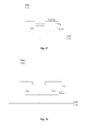
- FIG. 27 is a circuit diagram of a pixel unit when the region of the array substrate between the source electrode and the drain electrode is in an on state according to an embodiment of the present invention
- FIG. 28 is a circuit diagram of the pixel unit when the region of the array substrate between the source electrode and the drain electrode is in an off state according to an embodiment of the present invention
- FIG. 29 is a schematic view showing the array substrate where the pattern of the gate electrode is located at a side adjacent to the substrate according to an embodiment of the present invention.
- FIG. 30 is a schematic view showing the array substrate where the pattern of the gate electrode is located at a side away from the substrate according to an embodiment of the present invention.
- the present invention provides an array substrate with low power consumption.
- a gate insulating layer between source and drain electrodes and a pattern of a gate electrode has a thickness greater than that of the gate insulating layer between an active layer and the pattern of the gate electrode. Due to the thick gate insulating layer between the source and drain electrodes and the pattern of the gate electrode, the capacitance between the source and drain electrodes and the gate electrode will be reduced. In addition, the capacitance between the active layer and the pattern of the gate electrode remains unchanged. As a result, it is able to reduce the capacity of Cgs and Cgd corresponding to the source electrode and the drain electrode respectively and reduce the load of a pixel, thereby to reduce the power consumption of the entire display device.
- a method for manufacturing an array substrate comprises the steps of:
- Step 101 subjecting a gate insulating layer in a region between a source electrode and a drain electrode to a partial etching treatment by a one-time patterning process;
- Step 102 forming an active layer by a one-time patterning process, the active layer covering a partially-etched region of the gate insulating layer;
- Step 103 forming a pattern of a gate electrode by a one-time patterning process, the pattern of the gate electrode covering the partially-etched region of the gate insulating layer and a region of the gate insulating layer corresponding to the source and drain electrodes.
- the pattern of the gate electrode and the active layer are located at different sides of the gate insulating layer, and the gate insulating layer between the source and drain electrodes and the pattern of the gate electrode has a thickness greater than that of the gate insulating layer between the active layer, located between the source electrode and the drain electrode, and the pattern of the gate electrode.
- the Step 101 of subjecting the gate insulating layer in the region between the source electrode and the drain electrode to the partial etching treatment by a one-time patterning process comprises: subjecting the gate insulating layer in the region between the source electrode and the drain electrode to the partial etching treatment by a half-exposure process, and subjecting a via-hole region of the gate insulating layer to a full-exposure treatment, so as to form a via-hole in the gate insulating layer.
- a layer of photoresist is coated onto the gate insulating layer.
- the photoresist in a region between the source electrode and the drain electrode corresponding to the pattern of the gate electrode is subjected to a half-exposure treatment through a semipermeable membrane or grating, and the photoresist in a via-hole region corresponding to the pattern of the gate electrode is subjected to a full-exposure treatment. All the photoresist in the via-hole region, and the photoresist with a certain thickness that has been exposed in the region between the source electrode and the drain electrode, are removed through an exposure and development treatment.
- the gate insulating layer has a thickness of 6000 ⁇ to 8000 ⁇ in a region other than the region between the source electrode and the drain electrode, and the gate insulating layer has a thickness of 3000 ⁇ to 4000 ⁇ in the region between the source electrode and the drain electrode.
- Capacitors of a traditional TFT include a capacitor Cgs between the gate electrode and the source electrode, a capacitor Cga between the gate electrode and the active layer, and a capacitor Cgd between the gate electrode and the drain electrode.
- the capacitor Cga is mainly related to the electron distribution that will affect the properties of the TFT. The current flows through the capacitor Cga to form the channel, so that the electrons directionally migrate to a pixel electrode.
- the current is required to flow through the source electrode at first, then through the channel region and the drain electrode, and finally through a first ITO layer connected to the drain electrode, so as to transmit the current to the pixel electrode.
- the current flows through the source electrode and the drain electrode, due to the existence of the capacitors Cgs and Cgd, a relatively large current intensity is required to break energy barriers of Cgs and Cgd.
- it is required to provide a high voltage.
- the higher the voltage the higher the power consumption when the electric energy is converted into the other kind of energy, and as a result, unnecessary power consumption will occur.
- the capacitor formed by the active layer and the gate electrode is configured to form the channel after receiving the current, so the capacity of the capacitor shall not be too small. Otherwise, the current flowing therethrough will be small, and as a result, it is easy to cause a muted color excited in a pixel unit, thereby to cause an adverse display effect.
- the gate insulating layer between the active layer and the gate electrode has a thickness of 3000 ⁇ to 4000 ⁇ , which may be equal to a thickness of the gate insulating layer between the active layer and the gate electrode in the prior art.
- the capacity of Cga remains unchanged, i.e., it is able to ensure the capacity of Cga.
- Two different array substrates may be manufactured according to the method of the present invention, and these two conditions will be described hereinafter.
- the method for manufacturing the array substrate where the pattern of the gate electrode is located at a side adjacent to the substrate comprises the steps of:
- Step 201 forming the pattern of the gate electrode on the substrate
- Step 202 forming the gate insulating layer on the substrate with the pattern of the gate electrode;
- Step 203 forming the active layer on the gate insulating layer
- Step 204 forming the source electrode, the drain electrode and a pixel electrode layer on the active layer;
- Step 205 forming a passivation layer and a slit-like common electrode layer on the source electrodes, the drain electrodes and the pixel electrode layer, the pixel electrode being electrically connected to the drain electrode.
- Step 201 forming the pattern of the gate electrode on the substrate by a one-time patterning process.
- the gate insulating layer formed on the substrate with the pattern of the gate electrode has a thickness about twice the thickness of the gate insulating layer in the prior art, i.e., about 6000 ⁇ to 8000 ⁇ .
- Step 203 comprises: coating a layer of photoresist onto the gate insulating layer, subjecting the photoresist in the region between the source electrode and the drain electrode corresponding to the pattern of the gate electrode to a half-exposure treatment by an exposure and development process, and subjecting the photoresist in the via-hole region corresponding to the pattern of the gate electrode to a full-exposure treatment; removing all the photoresist in the via-hole region and the photoresist with a certain thickness that has been exposed in the region between the source electrode and the drain electrode through an exposure and development treatment; removing all the gate insulating layer corresponding to the via-hole region by an etching process to form a pattern of the via-hole; removing the remaining photoresist in the region between the source electrode and the drain electrode by an ashing process, and removing the gate insulating layer with a predetermined thickness in the region between the source electrode and the drain electrode by an etching process, so that the remaining gate insulating layer in the region between the source electrode and the
- the remaining gate insulating layer has a thickness of about 3000 ⁇ to 4000 ⁇ .
- the pattern of the via-hole and the pattern of the region between the source electrode and the drain electrode are formed by a one-time patterning process, while in the prior art, these patterns are formed by two patterning processes.
- the substrate with the pattern of the via-hole and the pattern of the region between the source electrode and the drain electrode are coated with a layer of photoresist, and the photoresist corresponding to the pattern of the region between the source electrode and the drain electrode is removed by the exposure and development process.
- a surface of the pattern of the region between the source electrode and the drain electrode is treated with hydrogen plasma, and then a layer of A ⁇ Si:H and a layer of N+Si:H are deposited on the pattern of the region between the source electrode and the drain electrode by a one-time patterning process, and the active layer is formed.
- N+Si:H is a semiconductor material and can produce electrons. When the current flows therethrough, it is able to weaken the energy barriers of the source electrode and the drain electrode.
- Step 204 comprises: forming the source electrodes and the drain electrodes on the substrate with the active layer by a one-time patterning process; depositing a layer of materials for forming the source electrode and the drain electrode on the pattern of the via-hole; and removing the materials for forming the source electrode and the drain electrode deposited on a pattern of the channel region by a one-time patterning process using a wet etching method, and removing N+Si:H deposited on the pattern of the channel region using a dry etching method.
- the materials for forming the source electrode and the drain electrode include, but not limited to, Mo, and Mo/Al/Mo.
- the first ITO layer is formed on the substrate with the source electrode and the drain electrode as the pixel electrode, and a pattern of the pixel electrode is formed so as to be connected to the drain electrode.
- Step 205 comprises: depositing the passivation layer on the substrate with the first ITO layer and forming the via-hole in the passivation layer by a one-time patterning process; depositing a second ITO layer on the substrate with the passivation layer, and etching the second ITO layer into a bar-like structure by a one-time patterning process, so as to form a pattern of the slit-like common electrode; and transmitting a signal to the source electrode, the drain electrode and the gate electrode through the second ITO layer and the via-hole in the passivation layer.
- the method for manufacturing the array substrate where the pattern of the gate electrode is located at a side adjacent to the substrate comprises the following steps.
- Step 301 forming the pattern of the gate electrode on the substrate by a one-time patterning process.
- FIG. 4 is a schematic view showing the substrate with the pattern of the gate electrode, where 401 represents the substrate, and 402 represents the pattern of the gate electrode.
- Step 302 depositing a layer of SiNx having a thickness of about 6000 ⁇ to 8000 ⁇ on the substrate with the pattern of the gate electrode, so as to form the gate insulating layer.
- FIG. 5 is a schematic view showing the substrate on which the gate insulating layer is deposited, where 501 represents the gate insulating layer.
- Step 303 coating a layer of photoresist onto the gate insulating layer, subjecting the photoresist in the region between the source electrode and the drain electrode corresponding to the pattern of the gate electrode to a half-exposure treatment through a semipermeable membrane or grating, and subjecting the photoresist in the via-hole region corresponding to the pattern of the gate electrode to a full-exposure treatment.
- 6 is a schematic view showing the substrate coated with the photoresist and being subjected to an exposure treatment, where 601 represents the layer of photoresist, 602 represents the photoresist in the region between the source electrode and the drain electrode that is subjected to the half-exposure treatment, and 603 represents the photoresist in the via-hole region that is subjected to the full-exposure treatment.
- Step 304 removing all the photoresist in the via-hole region and the photoresist with a certain thickness that has been exposed in the region between the source electrode and the drain electrode by an exposure and development treatment.
- FIG. 7 is a schematic view showing the substrate with the exposed photoresist being removed.
- Step 305 removing the entire gate insulating layer corresponding to the via-hole region by an etching process, so as to form the pattern of the via-hole.
- FIG. 8 is a schematic view showing the substrate with the pattern of the via-hole, where 801 represents the pattern of the via-hole.
- Step 306 removing the remaining photoresist in the region between the source electrode and the drain electrode by an ashing process.
- FIG. 9 is a schematic view showing the substrate treated with an ashing process.
- Step 307 removing the gate insulating layer having a predetermined thickness in the region between the source electrode and the drain electrode by an etching process, the remaining gate insulating layer may have a thickness of about 3000 ⁇ to 4000 ⁇ .
- FIG. 10 is a schematic view showing the substrate with the gate insulating layer, having a predetermined thickness in the region between the source electrode and the drain electrode, being removed, where 1001 represents the pattern of the region between the source electrode and the drain electrode.
- Step 308 depositing the layer of A ⁇ Si:H and the layer of N+Si:H on the pattern of the region between the source electrode and the drain electrode corresponding to the pattern of the gate electrode by a one-time patterning process, and forming an active layer.
- FIG. 11 is a schematic view showing the substrate with the active layer, where 1101 represents the layer of A ⁇ Si:H in the active layer, and 1102 represents the layer of N+Si:H in the active layer.
- Step 309 forming the patterns of the source electrode and the drain electrode on the substrate with the pattern of the active layer and the pattern of the via-hole by a one-time patterning process.
- FIG. 12 is a schematic view showing the substrate with the source electrode and the drain electrode, where 1201 represents the drain electrode, and 1202 represents the source electrode.
- Step 310 forming the first ITO layer on the substrate with the source electrode and the drain electrode by a one-time patterning process, and forming the pattern of the pixel electrode.
- FIG. 13 is a schematic view showing the substrate with the pattern of the pixel electrode, where 1301 represents the first ITO layer.
- Step 311 depositing the passivation layer on the substrate with the pattern of the pixel electrode, the passivation layer may have a thickness of 6000 ⁇ .
- FIG. 14 is a schematic view showing the substrate with the passivation layer, where 1401 represents the passivation layer.
- Step 312 forming the via-hole in the passivation layer by a one-time patterning process, and transmitting the signal to the source electrode, the drain electrode and the gate electrode through the via-hole.
- Step 313 depositing the second ITO layer on the substrate with the passivation layer, and etching the second ITO layer into a bar-like structure by a one-time patterning process, so as to form the pattern of the slit-like common electrode, thereby to form the array substrate.
- FIG. 15 is a schematic view showing the array substrate, where 1501 represents the second ITO layer.
- FIG. 16 is a sectional view of the array substrate at the via-hole in the passivation layer, where 1501 represents the second ITO layer, and 1601 represents the via-hole in the passivation layer.
- the method for manufacturing the array substrate where the pattern of the gate electrode is located at a side away from the substrate comprises the following steps:
- Step 1701 forming the active layer on the substrate
- Step 1702 forming the source electrodes, the drain electrodes and the pixel electrode layer on the active layer;
- Step 1703 forming the gate insulating layer on the source electrodes, the drain electrodes and the pixel electrode layer;
- Step 1704 forming the pattern of the gate electrode on the gate insulating layer.
- Step 1705 forming the passivation layer and the slit-like common electrode layer on the pattern of the gate electrode.
- Step 1701 comprises: depositing the layer of A ⁇ Si:H and the layer of N+Si:H on the substrate by a one-time patterning process, and forming the active layer.
- N+Si:H is a semiconductor material and can produce electrons. When the current flows therethrough, it is able to weaken the energy barriers of the source electrode and the drain electrode.
- Step 1702 comprises: forming the source electrodes and the drain electrodes on the substrate with the active layer by a one-time patterning process; depositing a layer of materials for forming the source electrode and the drain electrode on the pattern of the via-hole; and removing the materials for forming the source electrode and the drain electrode deposited on the pattern of the region between the source electrode and the drain electrode by a one-time patterning process using a wet etching method, and removing N+Si:H deposited on the pattern of the region between the source electrode and the drain electrode using a dry etching method.
- the materials for forming the source electrode and the drain electrode include, but not limited to, Mo, and Mo/Al/Mo.
- the first ITO layer is formed on the substrate with the source electrode and the drain electrode as the pixel electrode, and a pattern of the pixel electrode is formed so as to be connected to the drain electrode.
- Step 1703 forming the gate insulating layer having a thickness about twice the thickness of the gate insulating layer in the prior art, i.e., about 6000 ⁇ to 8000 ⁇ , on the substrate with the patterns of the source electrode and the drain electrode as well as the pattern of the active layer.
- Step 1703 the layer of photoresist is coated onto the gate insulating layer, the photoresist in the region between the source electrode and the drain electrode is subjected to a half-exposure treatment by an exposure and development process, and the photoresist in the via-hole region is subjected to a full-exposure treatment. All the photoresist in the via-hole region and the photoresist with a certain thickness that has been exposed in the region between the source electrode and the drain electrode are removed through an exposure and development treatment. The entire gate insulating layer in the via-hole region is removed by an etching process, and the pattern of the via-hole is formed.
- the remaining photoresist in the region between the source electrode and the drain electrode is removed by an ashing process, and the then the gate insulating layer having a predetermined thickness in the region between the source electrode and the drain electrode is removed by an etching process, so that the remaining gate insulating layer in the region between the source electrode and the drain electrode has a thickness substantially equal to the gate insulating layer in the prior art.
- the remaining the gate insulating layer may have a thickness of about 3000 ⁇ to 4000 ⁇ .
- Step 1704 comprises forming the pattern of the gate electrode on the substrate with the gate insulating layer.
- the gate insulating layer between the source and drain electrodes and the pattern of the gate electrode may have a thickness of about 6000 ⁇ to 8000 ⁇ , and a thickness of the gate insulating layer between the active layer and the pattern of the gate electrode may be 3000 ⁇ to 4000 ⁇ .
- Step 1705 comprises: depositing the passivation layer on the substrate with the pattern of gate electrode and forming the via-hole in the passivation layer by a one-time patterning process; depositing the second ITO layer on the substrate with the passivation layer, and etching the second ITO layer into a bar-like structure by a one-time patterning process so as to form the pattern of the slit-like common electrode; and transmitting the signal to the source electrode, the drain electrode and the gate electrode through the second ITO layer and the via-hole in the passivation layer.
- the method for manufacturing the array substrate where the pattern of the gate electrode is located at a side away from the substrate comprises the following steps.
- Step 1801 forming the active layer on the substrate by a one-time patterning process.
- FIG. 19 is a schematic view showing the substrate with the active layer, where 1901 represents the substrate, and 1902 represents the pattern of the active layer.
- Step 1802 forming the source electrode and the drain electrode on the substrate with the active layer by a one-time patterning process, and depositing a layer of materials for forming the source electrode and the drain electrode at the pattern of the via-hole.
- FIG. 20 is a schematic view showing the substrate on which the source electrode and the drain electrode are deposited, where 2001 represents the drain electrode, and 2002 represents the source electrode.
- Step 1803 forming the first ITO layer on the substrate with the source electrode and the drain electrode by a one-time patterning process, and forming the pattern of the pixel electrode.
- FIG. 21 is a schematic view showing the substrate with the pattern of the pixel electrode, where 2101 represents the first ITO layer.
- Step 1804 depositing a layer of SiNx having a thickness of 6000 ⁇ to 8000 ⁇ on the source electrodes, the drain electrodes and the pixel electrode layer, and forming the gate insulating layer.
- FIG. 22 is a schematic view showing the substrate on which the gate insulating layer is deposited, where 2201 represents the gate insulating layer.
- Step 1805 forming the pattern of the via-hole by a one-time patterning process, and removing the gate insulating layer having a predetermined thickness in the region between the source electrode and the drain electrode, the remaining gate insulating layer having a thickness of about 3000 ⁇ to 4000 ⁇ .
- FIG. 23 is a schematic view showing the substrate on which the pattern of the via-hole is formed and from which the gate insulating layer having a predetermined thickness in the region between the source electrode and the drain electrode is removed, where 2301 represents the pattern of the region between the source electrode and the drain electrode, and 2302 represents the pattern of the via-hole.
- Step 1806 forming the pattern of the gate electrode on the gate insulating layer by a one-time patterning process.
- FIG. 24 is a schematic view showing the substrate with the pattern of the gate electrode, where 2401 represents the pattern of the gate electrode.
- Step 1807 depositing the passivation layer on the substrate with the pattern of the gate electrode, the passivation layer having a thickness of 6000 ⁇ .
- FIG. 25 is a schematic view showing the substrate on which the passivation layer is deposited, where 2501 represents the passivation layer.
- Step 1808 forming the via-hole in the passivation layer by a one-time patterning process, and transmitting the signal to the source electrode, the drain electrode and the gate electrode through the via-hole.
- Step 1809 depositing the second ITO layer on the substrate with the passivation layer, and etching the second ITO layer into a bar-like structure by a one-time patterning process, so as to form the pattern of the slit-like common electrode, thereby to form the array substrate.
- FIG. 26 is a schematic view showing the array substrate, where 2601 represents the second ITO layer.
- FIG. 27 is a circuit diagram of a pixel unit when the region of the array substrate in the region between the source electrode and the drain electrode is in an on state.
- the source electrode and the gate electrode form the capacitor Cgs
- the drain electrode and the gate electrode form the capacitor Cgd
- the active layer and the gate electrode form the capacitor Cga.
- the capacitor Cga formed by the active layer and the gate electrode is located in the region between the active layer and the drain electrode, so as to form the channel after receiving the current, so the capacity of the capacitor shall not be too small. Otherwise, the current flowing therethrough will be relatively small, and as a result, it is easy to cause a muted color excited in a pixel unit, thereby to cause an adverse display effect.
- the capacitors formed by the source and drain electrodes and the gate electrode will block the flow of the current. When the current flows through these two capacitors, a relatively large current intensity is required so as to break the energy barriers of the capacitors, and a large amount of electric energy will be converted into thermal energy or the others. As a result, the energy loss will occur.
- the capacitors formed by the source and drain electrodes and the gate electrode are required to have small capacity.
- the gate insulating layer between the source and drain electrodes and the gate electrode has a thickness twice an ordinary insulating layer, so as to remarkably reduce the energy loss.
- the gate insulating layer between the active layer and the gate electrode has a small thickness, and the capacitor Cga formed thereby remains unchanged, i.e., it is able to ensure the capacity of the capacitor Cga and reduce the capacity of the capacitors Cgs and Cgd.
- I ds represents the current for the source and drain electrodes
- I on represents an on-state current for the channel
- ⁇ eff represents the equivalent carrier mobility
- ⁇ ins represents a dielectric constant of the gate insulating layer
- ⁇ 0 represents a vacuum dielectric constant
- t ins represents the thickness of the gate insulating layer in the region between the source electrode and the drain electrode
- ⁇ ins ⁇ 0 /t ins represents the capacitance of the gate insulating layer per unit area
- W represents a width of the region between the source electrode and the drain electrode
- L represents a length of the region between the source electrode and the drain electrode
- v gs represents a voltage between the gate electrode and the source electrode
- v ds represents a voltage between the gate electrode and the drain electrode
- v th represents a threshold voltage.
- FIG. 28 is a circuit diagram of the pixel unit when the region of the array substrate between the source electrode and the drain electrode is in an off state.
- the source electrode and the drain electrode form the capacitor Cgs
- the drain electrode and the gate electrode form the capacitor Cgd.
- Gate Line represents a gate line
- Data Line represents a data line. Because the capacity of the capacitors Cgd and Cgs decreases, the consumed electric energy will decrease too, and as a result, it is able to reduce the power consumption of the array substrate.
- the present invention further provides an array substrate.
- the principle of the array substrate for solving the technical problems is similar to that mentioned in the method for manufacturing an array substrate in the first embodiment, so the implementation of the array substrate may refer to those mentioned above, and it will not be repeated herein.
- the array substrate comprises a gate insulating layer; an active layer, a source electrode and a drain electrode covering one side of the gate insulating layer; and a pattern of a gate electrode covering the other side of the gate insulating layer.
- the gate insulating layer between the source and drain electrodes and the pattern of the gate electrode has a thickness greater than that of the gate insulating layer between the active layer, located between the source electrode and the drain electrode, and the pattern of the gate electrode.
- the array substrate where the pattern of the gate electrode is located at a side adjacent to a substrate comprises: the substrate 2901 ; the gate electrode 2902 formed on the substrate 2901 ; the gate insulating layer 2903 formed on the gate electrode and on a region of the substrate which is not covered by the gate electrode; the active layer 2904 formed on the pattern of the gate electrode; the source and drain electrodes 2905 and a pixel electrode 2907 formed on the active layer; a pattern 2906 of a via-hole formed on the gate insulating layer and connected to the pattern of the gate electrode; a first ITO layer 2907 formed on the gate insulating layer and connected to the drain electrode; a passivation layer 2908 covering the source electrode, the drain electrode, the first ITO layer and pattern of the via-hole; the via-hole (not shown) formed in the passivation layer; and a second ITO layer 2909 formed on the passivation layer.
- the gate insulating layer between the active layer and the pattern of the gate electrode may have a thickness of 3000 ⁇ to 4000 ⁇ , and the gate insulating layer between the source and drain electrodes and the pattern of the gate electrode may have a thickness of 6000 ⁇ to 8000 ⁇ .
- the pattern of the via-hole is covered with materials for forming the source electrode and the drain electrode, and the passivation layer may have a thickness of about 6000 ⁇ .
- a signal is transmitted to the source electrode, the drain electrode and the gate electrode through the second ITO layer and the via-hole in the passivation layer.
- the array substrate where the pattern of the gate electrode is located at a side away from the substrate comprises: the substrate 3001 ; the active layer 3002 formed on the substrate; a layer of the source and drain electrodes 3003 and the pixel electrode layer 3004 formed on the active layer; patterns 3005 of the source and drain electrodes formed on the substrate; the gate insulating layer 3006 formed on the source electrodes, the drain electrodes and the pixel electrode layer and above a region of the substrate which is not covered with the active layer; the pattern 3007 of the gate electrode formed on the gate insulating layer; the passivation layer 3008 covering the gate insulating layer 3006 and the pattern 3007 of the gate electrode; the via-hole (not shown) formed in the passivation layer; and the second ITO layer 3009 formed on the passivation layer.
- the pixel electrode is connected to the drain electrode.
- the pattern 3007 of the gate electrode is connected to the patterns 3005 of the source electrode and the drain electrode on the substrate through the pattern of the via-hole.
- the gate insulating layer between the active layer and the pattern of the gate electrode may have a thickness of 3000 ⁇ to 4000 ⁇ , and the gate insulating layer between the source and drain electrodes and the pattern of the gate electrode may have a thickness of 6000 ⁇ to 8000 ⁇ .
- the thickness of the passivation layer may be about 6000 ⁇ .
- the source electrode and the gate electrode form the capacitor Cgs
- the drain electrode and the gate electrode form the capacitor Cgd
- the active layer and the gate electrode form the capacitor Cga.
- the current flowing therethrough will be relatively small, and as a result, it is easy to cause a muted color excited in a pixel unit, thereby to cause an adverse display effect.
- the capacitors formed by the source and drain electrodes and the gate electrode will block the flow of the current.
- a relatively large current intensity is required so as to break the energy barriers of the capacitors, and a large amount of electric energy will be converted into thermal energy or the others. As a result, the energy loss will occur.
- the capacitors formed by the source and drain electrodes and the gate electrode are required to have small capacity.
- the gate insulating layer between the source and drain electrodes and the gate electrode has a thickness twice an ordinary insulating layer, so as to remarkably reduce the energy loss.
- the gate insulating layer between the active layer and the gate electrode has a small thickness, and the capacitor Cga formed thereby remains unchanged, i.e., it is able to ensure the capacity of the capacitor Cga and reduce the capacity of the capacitors Cgs and Cgd.
- the source electrode and the gate electrode form the capacitor Cgs
- the drain electrode and the gate electrode form the capacitor Cgd. Because the capacity of the capacitors Cgd and Cgs decreases, the consumed electric energy will decrease too, and as a result, it is able to reduce the power consumption of the array substrate.
- the present invention further provides a display device comprising any one of the above-mentioned array substrates.
Landscapes
- Physics & Mathematics (AREA)
- Nonlinear Science (AREA)
- Chemical & Material Sciences (AREA)
- Mathematical Physics (AREA)
- Crystallography & Structural Chemistry (AREA)
- General Physics & Mathematics (AREA)
- Optics & Photonics (AREA)
- Engineering & Computer Science (AREA)
- Microelectronics & Electronic Packaging (AREA)
- Chemical Kinetics & Catalysis (AREA)
- General Chemical & Material Sciences (AREA)
- Thin Film Transistor (AREA)
- Liquid Crystal (AREA)
- Geometry (AREA)
Abstract
Description
I ds =I on=μeff(εinsε0 /t ins)(W/L)(V gs −V th)V ds (1-1)
Claims (20)
Applications Claiming Priority (3)
| Application Number | Priority Date | Filing Date | Title |
|---|---|---|---|
| CN201410126488.2A CN103915380A (en) | 2014-03-31 | 2014-03-31 | Manufacturing method of array substrate, array substrate and display device |
| CN201410126488 | 2014-03-31 | ||
| CN201410126488.2 | 2014-03-31 |
Publications (2)
| Publication Number | Publication Date |
|---|---|
| US20150279866A1 US20150279866A1 (en) | 2015-10-01 |
| US9466620B2 true US9466620B2 (en) | 2016-10-11 |
Family
ID=51040970
Family Applications (1)
| Application Number | Title | Priority Date | Filing Date |
|---|---|---|---|
| US14/488,029 Expired - Fee Related US9466620B2 (en) | 2014-03-31 | 2014-09-16 | Method for manufacturing array substrate, array substrate, and display device |
Country Status (2)
| Country | Link |
|---|---|
| US (1) | US9466620B2 (en) |
| CN (1) | CN103915380A (en) |
Families Citing this family (6)
| Publication number | Priority date | Publication date | Assignee | Title |
|---|---|---|---|---|
| CN108666218A (en) * | 2017-03-29 | 2018-10-16 | 京东方科技集团股份有限公司 | Thin film transistor (TFT) and display base plate and preparation method thereof, display device |
| CN107768306A (en) * | 2017-10-12 | 2018-03-06 | 惠科股份有限公司 | Display panel and manufacturing method thereof |
| CN109712995B (en) * | 2019-01-30 | 2021-03-09 | 上海天马有机发光显示技术有限公司 | Display panel and display device |
| KR102948072B1 (en) | 2020-10-22 | 2026-04-03 | 삼성디스플레이 주식회사 | Display device and method for manufacturing the same |
| CN114220824B (en) * | 2021-12-20 | 2025-12-30 | 北海惠科光电技术有限公司 | Array substrate, manufacturing method and display panel |
| CN115390302A (en) * | 2022-08-23 | 2022-11-25 | 广州华星光电半导体显示技术有限公司 | Liquid crystal display panel and preparation method thereof |
Citations (5)
| Publication number | Priority date | Publication date | Assignee | Title |
|---|---|---|---|---|
| US6211928B1 (en) | 1996-03-26 | 2001-04-03 | Lg Electronics Inc. | Liquid crystal display and method for manufacturing the same |
| US20120107982A1 (en) * | 2010-04-26 | 2012-05-03 | Beijing Boe Optoelectronics Technology Co., Ltd. | Manufacturing method for array substrate with fringe field switching type thin film transistor liquid crystal display |
| CN102629046A (en) | 2011-06-29 | 2012-08-08 | 北京京东方光电科技有限公司 | Array substrate, manufacturing method of array substrate and liquid crystal display device |
| US20130037814A1 (en) * | 2011-08-09 | 2013-02-14 | Lg Display Co., Ltd., | Thin film transistor, method fabricating thereof, liquid crystal display device and method for fabricating the same |
| CN103489892A (en) | 2013-09-25 | 2014-01-01 | 北京京东方光电科技有限公司 | Array substrate, preparing method of array substrate and display device of array substrate |
-
2014
- 2014-03-31 CN CN201410126488.2A patent/CN103915380A/en active Pending
- 2014-09-16 US US14/488,029 patent/US9466620B2/en not_active Expired - Fee Related
Patent Citations (5)
| Publication number | Priority date | Publication date | Assignee | Title |
|---|---|---|---|---|
| US6211928B1 (en) | 1996-03-26 | 2001-04-03 | Lg Electronics Inc. | Liquid crystal display and method for manufacturing the same |
| US20120107982A1 (en) * | 2010-04-26 | 2012-05-03 | Beijing Boe Optoelectronics Technology Co., Ltd. | Manufacturing method for array substrate with fringe field switching type thin film transistor liquid crystal display |
| CN102629046A (en) | 2011-06-29 | 2012-08-08 | 北京京东方光电科技有限公司 | Array substrate, manufacturing method of array substrate and liquid crystal display device |
| US20130037814A1 (en) * | 2011-08-09 | 2013-02-14 | Lg Display Co., Ltd., | Thin film transistor, method fabricating thereof, liquid crystal display device and method for fabricating the same |
| CN103489892A (en) | 2013-09-25 | 2014-01-01 | 北京京东方光电科技有限公司 | Array substrate, preparing method of array substrate and display device of array substrate |
Non-Patent Citations (2)
| Title |
|---|
| First Chinese Office Action regarding Application No. 2014101264882 dated Jan. 12, 2016. English translation provided by Dragon Intellectual Property Law Firm. |
| Second Chinese Office Action regarding Application No. 2014101264882 dated May 12, 2016. English translation provided by Dragon Intellectual Property Law Firm. |
Also Published As
| Publication number | Publication date |
|---|---|
| US20150279866A1 (en) | 2015-10-01 |
| CN103915380A (en) | 2014-07-09 |
Similar Documents
| Publication | Publication Date | Title |
|---|---|---|
| US9466620B2 (en) | Method for manufacturing array substrate, array substrate, and display device | |
| CN104393000B (en) | Array substrate, manufacturing method thereof and display device | |
| KR101679252B1 (en) | Thin film transistor substrate and method of manufacturing the same and Display Device using the same | |
| CN103928470B (en) | A kind of oxide semiconductor TFT array substrate and its manufacturing method | |
| KR101321218B1 (en) | Tft substrate and method for manufacture thereof | |
| CN102842601B (en) | Array substrate and manufacture method thereof | |
| US20140346502A1 (en) | Semiconductor device | |
| US20110019117A1 (en) | Tft-lcd array substrate and manufacturing method thereof | |
| WO2016045241A1 (en) | Array substrate, manufacturing method thereof and display device | |
| US10177257B2 (en) | Thin film transistor, method for fabricating the same, display substrate and display device | |
| CN109037150A (en) | Metal oxide semiconductor films transistor (TFT) array substrate and preparation method thereof | |
| US20180151749A1 (en) | Thin Film Transistor, Array Substrate and Methods for Manufacturing and Driving the same and Display Device | |
| KR20110104299A (en) | Thin film transistor, manufacturing method and display substrate using thin film transistor | |
| CN103928399B (en) | Preparation method, tft array substrate and the display device of tft array substrate | |
| WO2018209736A1 (en) | Thin film transistor and manufacturing method therefor | |
| CN108695342A (en) | Production method, array substrate and the liquid crystal display panel of array substrate | |
| US20160284737A1 (en) | Display substrate, its manufacturing method, and display device | |
| US9741861B2 (en) | Display device and method for manufacturing the same | |
| US20160231629A1 (en) | Array substrate and manufacturing method thereof, and liquid crystal display panel | |
| CN102779783A (en) | Pixel structure, as well as manufacturing method and display device thereof | |
| WO2015096374A1 (en) | Array substrate and manufacturing method therefor, display device, and thin-film transistor | |
| US9269637B2 (en) | Thin film transistor substrate | |
| US8421941B2 (en) | TFT substrate and method of manufacturing the same | |
| CN105629598A (en) | FFS mode array substrate and manufacturing method | |
| CN105097826A (en) | Gate driver on array (GOA) unit, fabrication method thereof, display substrate and display device |
Legal Events
| Date | Code | Title | Description |
|---|---|---|---|
| AS | Assignment |
Owner name: BOE TECHNOLOGY GROUP CO., LTD., CHINA Free format text: ASSIGNMENT OF ASSIGNORS INTEREST;ASSIGNOR:ZHANG, JINZHONG;REEL/FRAME:033752/0289 Effective date: 20140904 Owner name: BEIJING BOE OPTOELECTRONICS TECHNOLOGY CO., LTD., Free format text: ASSIGNMENT OF ASSIGNORS INTEREST;ASSIGNOR:ZHANG, JINZHONG;REEL/FRAME:033752/0289 Effective date: 20140904 |
|
| STCF | Information on status: patent grant |
Free format text: PATENTED CASE |
|
| MAFP | Maintenance fee payment |
Free format text: PAYMENT OF MAINTENANCE FEE, 4TH YEAR, LARGE ENTITY (ORIGINAL EVENT CODE: M1551); ENTITY STATUS OF PATENT OWNER: LARGE ENTITY Year of fee payment: 4 |
|
| FEPP | Fee payment procedure |
Free format text: MAINTENANCE FEE REMINDER MAILED (ORIGINAL EVENT CODE: REM.); ENTITY STATUS OF PATENT OWNER: LARGE ENTITY |
|
| LAPS | Lapse for failure to pay maintenance fees |
Free format text: PATENT EXPIRED FOR FAILURE TO PAY MAINTENANCE FEES (ORIGINAL EVENT CODE: EXP.); ENTITY STATUS OF PATENT OWNER: LARGE ENTITY |
|
| STCH | Information on status: patent discontinuation |
Free format text: PATENT EXPIRED DUE TO NONPAYMENT OF MAINTENANCE FEES UNDER 37 CFR 1.362 |
|
| FP | Lapsed due to failure to pay maintenance fee |
Effective date: 20241011 |