US9462656B2 - Lamp base having integral semiconductor transient protection device - Google Patents
Lamp base having integral semiconductor transient protection device Download PDFInfo
- Publication number
- US9462656B2 US9462656B2 US14/572,224 US201414572224A US9462656B2 US 9462656 B2 US9462656 B2 US 9462656B2 US 201414572224 A US201414572224 A US 201414572224A US 9462656 B2 US9462656 B2 US 9462656B2
- Authority
- US
- United States
- Prior art keywords
- lamp base
- terminal
- protection device
- contact
- semiconductor
- Prior art date
- Legal status (The legal status is an assumption and is not a legal conclusion. Google has not performed a legal analysis and makes no representation as to the accuracy of the status listed.)
- Active, expires
Links
Images


Classifications
-
- H05B33/0887—
-
- H—ELECTRICITY
- H01—ELECTRIC ELEMENTS
- H01R—ELECTRICALLY-CONDUCTIVE CONNECTIONS; STRUCTURAL ASSOCIATIONS OF A PLURALITY OF MUTUALLY-INSULATED ELECTRICAL CONNECTING ELEMENTS; COUPLING DEVICES; CURRENT COLLECTORS
- H01R33/00—Coupling devices specially adapted for supporting apparatus and having one part acting as a holder providing support and electrical connection via a counterpart which is structurally associated with the apparatus, e.g. lamp holders; Separate parts thereof
- H01R33/945—Holders with built-in electrical component
- H01R33/95—Holders with built-in electrical component with fuse; with thermal switch
-
- H—ELECTRICITY
- H01—ELECTRIC ELEMENTS
- H01J—ELECTRIC DISCHARGE TUBES OR DISCHARGE LAMPS
- H01J5/00—Details relating to vessels or to leading-in conductors common to two or more basic types of discharge tubes or lamps
- H01J5/50—Means forming part of the tube or lamps for the purpose of providing electrical connection to it
- H01J5/54—Means forming part of the tube or lamps for the purpose of providing electrical connection to it supported by a separate part, e.g. base
-
- H—ELECTRICITY
- H01—ELECTRIC ELEMENTS
- H01J—ELECTRIC DISCHARGE TUBES OR DISCHARGE LAMPS
- H01J61/00—Gas-discharge or vapour-discharge lamps
- H01J61/02—Details
- H01J61/30—Vessels; Containers
- H01J61/32—Special longitudinal shape, e.g. for advertising purposes
- H01J61/327—"Compact"-lamps, i.e. lamps having a folded discharge path
-
- H—ELECTRICITY
- H01—ELECTRIC ELEMENTS
- H01J—ELECTRIC DISCHARGE TUBES OR DISCHARGE LAMPS
- H01J61/00—Gas-discharge or vapour-discharge lamps
- H01J61/02—Details
- H01J61/56—One or more circuit elements structurally associated with the lamp
-
- H—ELECTRICITY
- H01—ELECTRIC ELEMENTS
- H01K—ELECTRIC INCANDESCENT LAMPS
- H01K1/00—Details
- H01K1/62—One or more circuit elements structurally associated with the lamp
-
- H—ELECTRICITY
- H01—ELECTRIC ELEMENTS
- H01K—ELECTRIC INCANDESCENT LAMPS
- H01K1/00—Details
- H01K1/62—One or more circuit elements structurally associated with the lamp
- H01K1/66—One or more circuit elements structurally associated with the lamp with built-in fuse
-
- H—ELECTRICITY
- H05—ELECTRIC TECHNIQUES NOT OTHERWISE PROVIDED FOR
- H05B—ELECTRIC HEATING; ELECTRIC LIGHT SOURCES NOT OTHERWISE PROVIDED FOR; CIRCUIT ARRANGEMENTS FOR ELECTRIC LIGHT SOURCES, IN GENERAL
- H05B41/00—Circuit arrangements or apparatus for igniting or operating discharge lamps
- H05B41/14—Circuit arrangements
-
- H—ELECTRICITY
- H05—ELECTRIC TECHNIQUES NOT OTHERWISE PROVIDED FOR
- H05B—ELECTRIC HEATING; ELECTRIC LIGHT SOURCES NOT OTHERWISE PROVIDED FOR; CIRCUIT ARRANGEMENTS FOR ELECTRIC LIGHT SOURCES, IN GENERAL
- H05B47/00—Circuit arrangements for operating light sources in general, i.e. where the type of light source is not relevant
- H05B47/20—Responsive to malfunctions or to light source life; for protection
-
- F—MECHANICAL ENGINEERING; LIGHTING; HEATING; WEAPONS; BLASTING
- F21—LIGHTING
- F21K—NON-ELECTRIC LIGHT SOURCES USING LUMINESCENCE; LIGHT SOURCES USING ELECTROCHEMILUMINESCENCE; LIGHT SOURCES USING CHARGES OF COMBUSTIBLE MATERIAL; LIGHT SOURCES USING SEMICONDUCTOR DEVICES AS LIGHT-GENERATING ELEMENTS; LIGHT SOURCES NOT OTHERWISE PROVIDED FOR
- F21K9/00—Light sources using semiconductor devices as light-generating elements, e.g. using light-emitting diodes [LED] or lasers
- F21K9/20—Light sources comprising attachment means
- F21K9/23—Retrofit light sources for lighting devices with a single fitting for each light source, e.g. for substitution of incandescent lamps with bayonet or threaded fittings
-
- F—MECHANICAL ENGINEERING; LIGHTING; HEATING; WEAPONS; BLASTING
- F21—LIGHTING
- F21Y—INDEXING SCHEME ASSOCIATED WITH SUBCLASSES F21K, F21L, F21S and F21V, RELATING TO THE FORM OR THE KIND OF THE LIGHT SOURCES OR OF THE COLOUR OF THE LIGHT EMITTED
- F21Y2115/00—Light-generating elements of semiconductor light sources
- F21Y2115/10—Light-emitting diodes [LED]
-
- H—ELECTRICITY
- H05—ELECTRIC TECHNIQUES NOT OTHERWISE PROVIDED FOR
- H05B—ELECTRIC HEATING; ELECTRIC LIGHT SOURCES NOT OTHERWISE PROVIDED FOR; CIRCUIT ARRANGEMENTS FOR ELECTRIC LIGHT SOURCES, IN GENERAL
- H05B45/00—Circuit arrangements for operating light-emitting diodes [LED]
- H05B45/50—Circuit arrangements for operating light-emitting diodes [LED] responsive to malfunctions or undesirable behaviour of LEDs; responsive to LED life; Protective circuits
- H05B45/56—Circuit arrangements for operating light-emitting diodes [LED] responsive to malfunctions or undesirable behaviour of LEDs; responsive to LED life; Protective circuits involving measures to prevent abnormal temperature of the LEDs
-
- Y—GENERAL TAGGING OF NEW TECHNOLOGICAL DEVELOPMENTS; GENERAL TAGGING OF CROSS-SECTIONAL TECHNOLOGIES SPANNING OVER SEVERAL SECTIONS OF THE IPC; TECHNICAL SUBJECTS COVERED BY FORMER USPC CROSS-REFERENCE ART COLLECTIONS [XRACs] AND DIGESTS
- Y02—TECHNOLOGIES OR APPLICATIONS FOR MITIGATION OR ADAPTATION AGAINST CLIMATE CHANGE
- Y02B—CLIMATE CHANGE MITIGATION TECHNOLOGIES RELATED TO BUILDINGS, e.g. HOUSING, HOUSE APPLIANCES OR RELATED END-USER APPLICATIONS
- Y02B20/00—Energy efficient lighting technologies, e.g. halogen lamps or gas discharge lamps
- Y02B20/30—Semiconductor lamps, e.g. solid state lamps [SSL] light emitting diodes [LED] or organic LED [OLED]
Definitions
- LED lighting has application in both residential and commercial implementations. LED lighting provides low maintenance costs, long life and reduced power consumption compared to more conventional lighting technologies. Another energy saving lighting technology is compact fluorescent lamps (CFL).
- CFL compact fluorescent lamps
- Lamps having LED light sources or CFL light sources can be susceptible to overvoltage transients.
- the electronics that drive the LED or CFL lamp needs to be protected from transients.
- a metal oxide varistor (MOV) can protect the LED, or CFL, lamp's driver electronics from overvoltage surges by clamping short duration voltage impulses.
- the MOV component can be placed on the circuit board containing the driver electronics (across the AC power input) so as to provide the overvoltage clamping protection against lightning-related, switching, and/or other electrical transients.
- FIG. 1 depicts a perspective view of a conventional lamp base
- FIG. 2 depicts a schematic of a semiconductor transient protection device in accordance with some embodiments
- FIG. 3A is a bottom view of semiconductor transient protection device in accordance with some embodiments.
- FIG. 3B is a cross-sectional view of the semiconductor transient protection device of FIG. 3A along line A-A;
- FIG. 4A is a plan view of a lamp base having a semiconductor transient protection device in accordance with some embodiments.
- FIG. 4B is a cross-sectional view of the lamp base of FIG. 4A along line A-A.
- the construction of the lamp base itself includes the MOV, or other transient protection device, as a replacement for the conventional insulator incorporated within the lamp base.
- a thermal limiting circuit e.g., a fuse or resistor
- FIG. 1 depicts a bottom perspective view of conventional lamp base 100 .
- the conventional lamp base can be, for example, an Edison base E27 or E15, or other type lamp base.
- Lamp base 100 includes neutral contact 110 , which is typically a large conductive metal surface area around the circumference of the lamp base.
- Line contact 120 is typically a smaller conductive metal surface located at the bottom of the lamp base. Isolating the neutral and line contacts is insulator 130 located between the contacts.
- the conventional insulator is a non-semiconductor, ceramic insulator that both electrically and mechanically isolates the neutral and line contacts.
- a three-way lamp base includes an additional contact and isolator.
- a semiconductor transient protection device replaces the conventional ceramic isolator in the lamp base construction.
- This semiconductor transient protection device can be an MOV, a transient voltage suppression (TVS) diode, and other voltage-clamping devices.
- the semiconductor transient protection device acts to isolate the neutral and line contacts of the lamp base from each other.
- the semiconductor provides a shunt path between the line contact and the neutral contact to protect the driver electronics located within the lamp base.
- the amount of excess voltage on the line contact can be predetermined by parameters of a semiconductor element with the transient protection device.
- the shunt path provided by the semiconductor element can be a low resistance path based on the parameters of the semiconductor element.
- FIG. 2 schematically depicts three-terminal semiconductor transient protection device 200 in accordance with some embodiments.
- Embodying devices include line input 210 and neutral input 220 .
- the neutral input is provided to the lamp's driver electronics mounted on a circuit board.
- thermal element 225 In series with the line input is thermal element 225 , which is depicted as a fusible resistor in FIG. 2 .
- the invention is not so limited, and other thermal elements which offer protection to high current conditions can also be implemented in semiconductor transient protection device 200 .
- the thermal element limits current into the MOV or into the electronics protected in series with it, which can make the product safer and allow for reduced size of the lamp's internal electronics.
- Semiconductor element 230 can be a two terminal device connected between the neutral line to the lamp and protected line input 240 .
- Semiconductor element 230 is depicted as a metal oxide varistor in FIG. 2 .
- the invention is not so limited, and other semiconductor elements can also be implemented in semiconductor transient protection device 200 .
- One side of thermal link is connected at the junction of the semiconductor element and the protected line input.
- FIG. 3A is a bottom view of three-terminal semiconductor transient protection device 300 in accordance with some embodiments.
- FIG. 3B is a cross-sectional view of three-terminal semiconductor transient protection device 300 along line A-A.
- the three-terminal semiconductor transient protection device includes semiconductor element 310 (e.g., a MOV, a TVS diode, etc.) across the output lines connected to the lamp's electronics and thermal element 320 (e.g., a fusible resistor, etc.) in series with the line voltage input.
- a lead-in wire ( FIG. 4B ; item 460 ) passes through central aperture 330 of the three-terminal semiconductor device to connect the junction of the thermal element and the semiconductor element with the line input of the electronic drive circuitry.
- Embodying devices can be constructed so that the semiconductor element is in contact with the neutral contact—i.e., a conductive metal-shell surface area around the circumference of the lamp base.
- the thermal link would be positioned to be in contact with the line contact of the lamp base, which is located at the bottom center of the lamp base.
- Embodying devices can be configured to accommodate a three-way lamp base having one neutral contact and two line contacts.
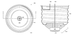
- FIG. 4A is a plan view of lamp base 400 having three-terminal semiconductor transient protection device 410 in accordance with some embodiments.
- FIG. 4B is a cross-sectional view of lamp base 400 along line A-A.
- three-terminal semiconductor transient protection device 410 includes semiconductor element 420 and thermal element 430 .
- Semiconductor element 420 is in electrical and mechanical contact with conductive metal-shell, neutral contact 440 of the lamp base. The semiconductor element is also in contact with the thermal element. Thermal element is in electrical and mechanical contact with line contact 470 of the lamp base.
- connection between the lamp base neutral contact and the neutral input of the driver circuit can be achieved by conductive mechanical connection to the conductive metal shell itself.
- extending from neutral contact 440 is lead-in wire 450 which connects with a neutral line input of an electronic driver circuit within the lamp base.
- Extending from the thermal element is lead-in wire 460 , which provides a protected line input to the electronic driver circuit.
- embodying devices may provide additional safety features to contain any spark, or flame, caused by the failure mode of the semiconductor element.
- the thermal element which is implemented as a fusible link, enhances these safety features by opening the line input circuit at a predetermined I 2 T level within the lamp base.
- Embodying devices which incorporate the semiconductor transient protection device as an integral component of a lamp base during manufacture may remove the need to incorporate a surge protection circuit in the driver circuitry of the electronic circuit board, which can save both space on the driver circuit board and reduce its manufacturing cost.
- the transient protection circuitry is among the largest volume components of many lamp designs. Having the protection circuitry built-in to the lamp base for CFL and LED lamps achieves cost and volume reductions. Further, an embodying semiconductor transient protection device can provide a more reliable lamp with fewer field returns.
- a CFL and/or a LED lamp can include an embodying lamp base with built-in protection circuitry.
- the embodying lamp base can include a neutral contact having a first conductive metal surface, a line contact having a second conductive metal surface, a semiconductor transient protection device having three terminals, the semiconductor transient protection device formed as an integral component of the lamp base, a first terminal of the semiconductor transient protection device in mechanical and electrical contact with the neutral contact, a second terminal of the semiconductor transient protection device in mechanical and electrical contact with the line contact, a third terminal of the semiconductor transient protection device in electrical contact with a lead-in wire, a thermal element in series with the first terminal and the third terminal, the third terminal being a surface of the thermal element, a two-terminal semiconductor element in electrical connection with the first terminal and the third terminal, the two-terminal semiconductor element having an aperture in which the lead-in wire is located, and the semiconductor transient protection device configured to isolate the line contact from the neutral contact during a first line voltage input, and to provide a low-re
Landscapes
- Circuit Arrangement For Electric Light Sources In General (AREA)
- Led Device Packages (AREA)
Abstract
Description
Claims (9)
Priority Applications (3)
| Application Number | Priority Date | Filing Date | Title |
|---|---|---|---|
| US14/572,224 US9462656B2 (en) | 2014-12-16 | 2014-12-16 | Lamp base having integral semiconductor transient protection device |
| PCT/US2015/058907 WO2016099683A1 (en) | 2014-12-16 | 2015-11-04 | Lamp base having integral semiconductor transient protection device |
| TW104140312A TW201633851A (en) | 2014-12-16 | 2015-12-02 | Lamp base having integral semiconductor transient protection device |
Applications Claiming Priority (1)
| Application Number | Priority Date | Filing Date | Title |
|---|---|---|---|
| US14/572,224 US9462656B2 (en) | 2014-12-16 | 2014-12-16 | Lamp base having integral semiconductor transient protection device |
Publications (2)
| Publication Number | Publication Date |
|---|---|
| US20160174328A1 US20160174328A1 (en) | 2016-06-16 |
| US9462656B2 true US9462656B2 (en) | 2016-10-04 |
Family
ID=54602025
Family Applications (1)
| Application Number | Title | Priority Date | Filing Date |
|---|---|---|---|
| US14/572,224 Active 2034-12-22 US9462656B2 (en) | 2014-12-16 | 2014-12-16 | Lamp base having integral semiconductor transient protection device |
Country Status (3)
| Country | Link |
|---|---|
| US (1) | US9462656B2 (en) |
| TW (1) | TW201633851A (en) |
| WO (1) | WO2016099683A1 (en) |
Families Citing this family (1)
| Publication number | Priority date | Publication date | Assignee | Title |
|---|---|---|---|---|
| US11362513B2 (en) * | 2017-03-07 | 2022-06-14 | Littelfuse Semiconductor (Wuxi) Co., Ltd. | Hybrid overvoltage protection device and assembly |
Citations (14)
| Publication number | Priority date | Publication date | Assignee | Title |
|---|---|---|---|---|
| US2197230A (en) * | 1937-12-20 | 1940-04-16 | Wilcolator Co | Thermostatic control |
| US3464048A (en) | 1967-10-16 | 1969-08-26 | Grayson G Stiles | Blowgun fuse adapter |
| US3930183A (en) * | 1973-04-30 | 1975-12-30 | Gen Electric | Incandescent lamps having protection against voltage surges |
| EP0957310A1 (en) | 1998-03-24 | 1999-11-17 | Powerone Electronic Co. Ltd. | PL Lamp holder |
| US20040166720A1 (en) * | 2003-02-25 | 2004-08-26 | Gibboney James W. | Safety light socket |
| US20100127625A1 (en) | 2008-11-26 | 2010-05-27 | Abl Ip Holding Llc | Surge Protection Module for Luminaires and Lighting Control Devices |
| US20110080740A1 (en) * | 2009-10-02 | 2011-04-07 | Lumination Llc | Led lamp with uniform omnidirectional light intensity output |
| US20110109164A1 (en) * | 2008-12-08 | 2011-05-12 | Tycka Design Private Limited | Intuitive Electronic Circuit |
| US20110193491A1 (en) * | 2010-02-05 | 2011-08-11 | Luxera, Inc. | Integrated Electronic Device for Controlling Light Emitting Diodes |
| US20110198996A1 (en) | 2010-02-12 | 2011-08-18 | Wen-Cheng Lai | Lighting Lamp Apparatus With Replaceable Fuse Element |
| US20110242816A1 (en) * | 2010-04-02 | 2011-10-06 | GE Lighting Solutions, LLC | Lightweight heat sinks and led lamps employing same |
| US20140340884A1 (en) * | 2013-05-17 | 2014-11-20 | Lightel Technologies, Inc. | Linear solid-state lighting with readily retrofittable modular structure |
| US20140375211A1 (en) * | 2013-06-19 | 2014-12-25 | Felipe A. Herrador | Led driver |
| US20150054338A1 (en) * | 2008-12-08 | 2015-02-26 | Shailendra Kumar Suman | Intuitive Electronic Circuit |
-
2014
- 2014-12-16 US US14/572,224 patent/US9462656B2/en active Active
-
2015
- 2015-11-04 WO PCT/US2015/058907 patent/WO2016099683A1/en not_active Ceased
- 2015-12-02 TW TW104140312A patent/TW201633851A/en unknown
Patent Citations (14)
| Publication number | Priority date | Publication date | Assignee | Title |
|---|---|---|---|---|
| US2197230A (en) * | 1937-12-20 | 1940-04-16 | Wilcolator Co | Thermostatic control |
| US3464048A (en) | 1967-10-16 | 1969-08-26 | Grayson G Stiles | Blowgun fuse adapter |
| US3930183A (en) * | 1973-04-30 | 1975-12-30 | Gen Electric | Incandescent lamps having protection against voltage surges |
| EP0957310A1 (en) | 1998-03-24 | 1999-11-17 | Powerone Electronic Co. Ltd. | PL Lamp holder |
| US20040166720A1 (en) * | 2003-02-25 | 2004-08-26 | Gibboney James W. | Safety light socket |
| US20100127625A1 (en) | 2008-11-26 | 2010-05-27 | Abl Ip Holding Llc | Surge Protection Module for Luminaires and Lighting Control Devices |
| US20150054338A1 (en) * | 2008-12-08 | 2015-02-26 | Shailendra Kumar Suman | Intuitive Electronic Circuit |
| US20110109164A1 (en) * | 2008-12-08 | 2011-05-12 | Tycka Design Private Limited | Intuitive Electronic Circuit |
| US20110080740A1 (en) * | 2009-10-02 | 2011-04-07 | Lumination Llc | Led lamp with uniform omnidirectional light intensity output |
| US20110193491A1 (en) * | 2010-02-05 | 2011-08-11 | Luxera, Inc. | Integrated Electronic Device for Controlling Light Emitting Diodes |
| US20110198996A1 (en) | 2010-02-12 | 2011-08-18 | Wen-Cheng Lai | Lighting Lamp Apparatus With Replaceable Fuse Element |
| US20110242816A1 (en) * | 2010-04-02 | 2011-10-06 | GE Lighting Solutions, LLC | Lightweight heat sinks and led lamps employing same |
| US20140340884A1 (en) * | 2013-05-17 | 2014-11-20 | Lightel Technologies, Inc. | Linear solid-state lighting with readily retrofittable modular structure |
| US20140375211A1 (en) * | 2013-06-19 | 2014-12-25 | Felipe A. Herrador | Led driver |
Non-Patent Citations (1)
| Title |
|---|
| PCT Search Report and Written Opinion issued in connection with corresponding PCT Application No. PCT/US2015/058907 on Feb. 24, 2016. |
Also Published As
| Publication number | Publication date |
|---|---|
| TW201633851A (en) | 2016-09-16 |
| WO2016099683A1 (en) | 2016-06-23 |
| US20160174328A1 (en) | 2016-06-16 |
Similar Documents
| Publication | Publication Date | Title |
|---|---|---|
| US8816812B2 (en) | Varistor fuse element | |
| EP3028541A1 (en) | Led replacement lamp for safe operation with electro-magnetic ballast | |
| US9872360B2 (en) | Photocontrol with surge protecting function | |
| CN107851990A (en) | Interphase surge protection device | |
| RU2663816C2 (en) | Led based replacement lamp for safe operation under the failure condition | |
| CN109313875B (en) | Modules for providing intrinsically safe electrical output power and explosion proof lamps | |
| US10098200B2 (en) | Photocontrol device with a surge protection function | |
| CN102074428B (en) | Switch module | |
| US20160359312A1 (en) | Surge protector having both fuse and alert functions | |
| JP2015135814A (en) | Ceramic chip fuse with offset fuse element | |
| US9000672B2 (en) | Connector with surge protection structure | |
| US9462656B2 (en) | Lamp base having integral semiconductor transient protection device | |
| US7973324B2 (en) | Lamp type light emitting device for safety fuse | |
| US20090237198A1 (en) | Safety power disconnection terminal apparatus with light indication | |
| US9933147B2 (en) | Terminal block assembly | |
| TWM512834U (en) | Power socket with over-current protection mechanism | |
| US10161571B1 (en) | LED tube with safety device | |
| US20120081004A1 (en) | Light emitting diode system | |
| KR101390387B1 (en) | System preventing thermal runway for varistor | |
| US10652982B2 (en) | Open-mode protection device and electronic device having same | |
| WO2015124520A1 (en) | Led circuit with surge protection | |
| US20100060408A1 (en) | Fuse module with indicating capability | |
| KR100842796B1 (en) | Lightning arrester disconnector | |
| KR20160071546A (en) | Lighting apparatus using pn junction light emitting means | |
| KR200456266Y1 (en) | fuse device |
Legal Events
| Date | Code | Title | Description |
|---|---|---|---|
| AS | Assignment |
Owner name: GE LIGHTING SOLUTIONS, LLC, OHIO Free format text: ASSIGNMENT OF ASSIGNORS INTEREST;ASSIGNORS:ROBERTS, BRUCE RICHARD;KNAPP, THOMAS ALEXANDER;TAUBERT, TIMOTHY A.;REEL/FRAME:034520/0773 Effective date: 20141215 |
|
| STCF | Information on status: patent grant |
Free format text: PATENTED CASE |
|
| MAFP | Maintenance fee payment |
Free format text: PAYMENT OF MAINTENANCE FEE, 4TH YEAR, LARGE ENTITY (ORIGINAL EVENT CODE: M1551); ENTITY STATUS OF PATENT OWNER: LARGE ENTITY Year of fee payment: 4 |
|
| AS | Assignment |
Owner name: PNC BANK, NATIONAL ASSOCIATION, PENNSYLVANIA Free format text: SECURITY INTEREST;ASSIGNORS:SAVANT SYSTEMS, INC.;CONSUMER LIGHTING (U.S.), LLC;REEL/FRAME:053095/0001 Effective date: 20200630 |
|
| AS | Assignment |
Owner name: CONSUMER LIGHTING, LLC, OHIO Free format text: ASSIGNMENT OF ASSIGNORS INTEREST;ASSIGNOR:CURRENT LIGHTING SOLUTIONS, LLC (FKA - GE LIGHTING SOLUTIONS, LLC);REEL/FRAME:059582/0748 Effective date: 20200224 |
|
| AS | Assignment |
Owner name: RACEPOINT ENERGY, LLC, OHIO Free format text: RELEASE BY SECURED PARTY;ASSIGNOR:PNC BANK, NATIONAL ASSOCIATION;REEL/FRAME:059910/0312 Effective date: 20220331 Owner name: SAVANT TECHNOLOGIES LLC, OHIO Free format text: RELEASE BY SECURED PARTY;ASSIGNOR:PNC BANK, NATIONAL ASSOCIATION;REEL/FRAME:059910/0312 Effective date: 20220331 Owner name: SAVANT SYSTEMS, INC., MASSACHUSETTS Free format text: RELEASE BY SECURED PARTY;ASSIGNOR:PNC BANK, NATIONAL ASSOCIATION;REEL/FRAME:059910/0312 Effective date: 20220331 |
|
| AS | Assignment |
Owner name: CURRENT LIGHTING SOLUTIONS, LLC, OHIO Free format text: CHANGE OF NAME;ASSIGNOR:GE LIGHTING SOLUTIONS, LLC;REEL/FRAME:060390/0276 Effective date: 20190401 |
|
| MAFP | Maintenance fee payment |
Free format text: PAYMENT OF MAINTENANCE FEE, 8TH YEAR, LARGE ENTITY (ORIGINAL EVENT CODE: M1552); ENTITY STATUS OF PATENT OWNER: LARGE ENTITY Year of fee payment: 8 |