US9461581B2 - Shadowing compensation device for solar cell module - Google Patents

Shadowing compensation device for solar cell module Download PDF

Info

Publication number
US9461581B2
US9461581B2 US14/072,875 US201314072875A US9461581B2 US 9461581 B2 US9461581 B2 US 9461581B2 US 201314072875 A US201314072875 A US 201314072875A US 9461581 B2 US9461581 B2 US 9461581B2
Authority
US
United States
Prior art keywords
solar cell
cell module
output
compensation device
shaded
Prior art date
Legal status (The legal status is an assumption and is not a legal conclusion. Google has not performed a legal analysis and makes no representation as to the accuracy of the status listed.)
Active, expires
Application number
US14/072,875
Other versions
US20150122312A1 (en
Inventor
Ya-Tsung Feng
Jia-Min Shen
Wen-Jie Hou
Current Assignee (The listed assignees may be inaccurate. Google has not performed a legal analysis and makes no representation or warranty as to the accuracy of the list.)
Ablerex Electronics Co Ltd
Original Assignee
Ablerex Electronics Co Ltd
Priority date (The priority date is an assumption and is not a legal conclusion. Google has not performed a legal analysis and makes no representation as to the accuracy of the date listed.)
Filing date
Publication date
Application filed by Ablerex Electronics Co Ltd filed Critical Ablerex Electronics Co Ltd
Priority to US14/072,875 priority Critical patent/US9461581B2/en
Assigned to ABLEREX ELECTRONICS CO., LTD. reassignment ABLEREX ELECTRONICS CO., LTD. ASSIGNMENT OF ASSIGNORS INTEREST (SEE DOCUMENT FOR DETAILS). Assignors: FENG, YA-TSUNG, HOU, Wen-jie, SHEN, JIA-MIN
Publication of US20150122312A1 publication Critical patent/US20150122312A1/en
Application granted granted Critical
Publication of US9461581B2 publication Critical patent/US9461581B2/en
Active legal-status Critical Current
Adjusted expiration legal-status Critical

Links

Images

Classifications

    • HELECTRICITY
    • H02GENERATION; CONVERSION OR DISTRIBUTION OF ELECTRIC POWER
    • H02JCIRCUIT ARRANGEMENTS OR SYSTEMS FOR SUPPLYING OR DISTRIBUTING ELECTRIC POWER; SYSTEMS FOR STORING ELECTRIC ENERGY
    • H02J3/00Circuit arrangements for ac mains or ac distribution networks
    • H02J3/38Arrangements for parallely feeding a single network by two or more generators, converters or transformers
    • H02J3/381Dispersed generators
    • HELECTRICITY
    • H02GENERATION; CONVERSION OR DISTRIBUTION OF ELECTRIC POWER
    • H02SGENERATION OF ELECTRIC POWER BY CONVERSION OF INFRARED RADIATION, VISIBLE LIGHT OR ULTRAVIOLET LIGHT, e.g. USING PHOTOVOLTAIC [PV] MODULES
    • H02S50/00Monitoring or testing of PV systems, e.g. load balancing or fault identification
    • HELECTRICITY
    • H01ELECTRIC ELEMENTS
    • H01LSEMICONDUCTOR DEVICES NOT COVERED BY CLASS H10
    • H01L31/00Semiconductor devices sensitive to infrared radiation, light, electromagnetic radiation of shorter wavelength or corpuscular radiation and specially adapted either for the conversion of the energy of such radiation into electrical energy or for the control of electrical energy by such radiation; Processes or apparatus specially adapted for the manufacture or treatment thereof or of parts thereof; Details thereof
    • H01L31/02Details
    • H01L31/02016Circuit arrangements of general character for the devices
    • H01L31/02019Circuit arrangements of general character for the devices for devices characterised by at least one potential jump barrier or surface barrier
    • H01L31/02021Circuit arrangements of general character for the devices for devices characterised by at least one potential jump barrier or surface barrier for solar cells
    • H02J3/383
    • HELECTRICITY
    • H02GENERATION; CONVERSION OR DISTRIBUTION OF ELECTRIC POWER
    • H02MAPPARATUS FOR CONVERSION BETWEEN AC AND AC, BETWEEN AC AND DC, OR BETWEEN DC AND DC, AND FOR USE WITH MAINS OR SIMILAR POWER SUPPLY SYSTEMS; CONVERSION OF DC OR AC INPUT POWER INTO SURGE OUTPUT POWER; CONTROL OR REGULATION THEREOF
    • H02M3/00Conversion of dc power input into dc power output
    • H02M3/22Conversion of dc power input into dc power output with intermediate conversion into ac
    • H02M3/24Conversion of dc power input into dc power output with intermediate conversion into ac by static converters
    • H02M3/28Conversion of dc power input into dc power output with intermediate conversion into ac by static converters using discharge tubes with control electrode or semiconductor devices with control electrode to produce the intermediate ac
    • H02M3/325Conversion of dc power input into dc power output with intermediate conversion into ac by static converters using discharge tubes with control electrode or semiconductor devices with control electrode to produce the intermediate ac using devices of a triode or a transistor type requiring continuous application of a control signal
    • H02M3/335Conversion of dc power input into dc power output with intermediate conversion into ac by static converters using discharge tubes with control electrode or semiconductor devices with control electrode to produce the intermediate ac using devices of a triode or a transistor type requiring continuous application of a control signal using semiconductor devices only
    • HELECTRICITY
    • H02GENERATION; CONVERSION OR DISTRIBUTION OF ELECTRIC POWER
    • H02JCIRCUIT ARRANGEMENTS OR SYSTEMS FOR SUPPLYING OR DISTRIBUTING ELECTRIC POWER; SYSTEMS FOR STORING ELECTRIC ENERGY
    • H02J2300/00Systems for supplying or distributing electric power characterised by decentralized, dispersed, or local generation
    • H02J2300/20The dispersed energy generation being of renewable origin
    • H02J2300/22The renewable source being solar energy
    • H02J2300/24The renewable source being solar energy of photovoltaic origin
    • HELECTRICITY
    • H02GENERATION; CONVERSION OR DISTRIBUTION OF ELECTRIC POWER
    • H02MAPPARATUS FOR CONVERSION BETWEEN AC AND AC, BETWEEN AC AND DC, OR BETWEEN DC AND DC, AND FOR USE WITH MAINS OR SIMILAR POWER SUPPLY SYSTEMS; CONVERSION OF DC OR AC INPUT POWER INTO SURGE OUTPUT POWER; CONTROL OR REGULATION THEREOF
    • H02M1/00Details of apparatus for conversion
    • H02M1/0083Converters characterised by their input or output configuration
    • H02M1/0093Converters characterised by their input or output configuration wherein the output is created by adding a regulated voltage to or subtracting it from an unregulated input
    • H02M2001/0093
    • HELECTRICITY
    • H02GENERATION; CONVERSION OR DISTRIBUTION OF ELECTRIC POWER
    • H02MAPPARATUS FOR CONVERSION BETWEEN AC AND AC, BETWEEN AC AND DC, OR BETWEEN DC AND DC, AND FOR USE WITH MAINS OR SIMILAR POWER SUPPLY SYSTEMS; CONVERSION OF DC OR AC INPUT POWER INTO SURGE OUTPUT POWER; CONTROL OR REGULATION THEREOF
    • H02M3/00Conversion of dc power input into dc power output
    • H02M3/22Conversion of dc power input into dc power output with intermediate conversion into ac
    • H02M3/24Conversion of dc power input into dc power output with intermediate conversion into ac by static converters
    • H02M3/28Conversion of dc power input into dc power output with intermediate conversion into ac by static converters using discharge tubes with control electrode or semiconductor devices with control electrode to produce the intermediate ac
    • H02M3/325Conversion of dc power input into dc power output with intermediate conversion into ac by static converters using discharge tubes with control electrode or semiconductor devices with control electrode to produce the intermediate ac using devices of a triode or a transistor type requiring continuous application of a control signal
    • H02M3/335Conversion of dc power input into dc power output with intermediate conversion into ac by static converters using discharge tubes with control electrode or semiconductor devices with control electrode to produce the intermediate ac using devices of a triode or a transistor type requiring continuous application of a control signal using semiconductor devices only
    • H02M3/33507Conversion of dc power input into dc power output with intermediate conversion into ac by static converters using discharge tubes with control electrode or semiconductor devices with control electrode to produce the intermediate ac using devices of a triode or a transistor type requiring continuous application of a control signal using semiconductor devices only with automatic control of the output voltage or current, e.g. flyback converters
    • HELECTRICITY
    • H02GENERATION; CONVERSION OR DISTRIBUTION OF ELECTRIC POWER
    • H02MAPPARATUS FOR CONVERSION BETWEEN AC AND AC, BETWEEN AC AND DC, OR BETWEEN DC AND DC, AND FOR USE WITH MAINS OR SIMILAR POWER SUPPLY SYSTEMS; CONVERSION OF DC OR AC INPUT POWER INTO SURGE OUTPUT POWER; CONTROL OR REGULATION THEREOF
    • H02M3/00Conversion of dc power input into dc power output
    • H02M3/22Conversion of dc power input into dc power output with intermediate conversion into ac
    • H02M3/24Conversion of dc power input into dc power output with intermediate conversion into ac by static converters
    • H02M3/28Conversion of dc power input into dc power output with intermediate conversion into ac by static converters using discharge tubes with control electrode or semiconductor devices with control electrode to produce the intermediate ac
    • H02M3/325Conversion of dc power input into dc power output with intermediate conversion into ac by static converters using discharge tubes with control electrode or semiconductor devices with control electrode to produce the intermediate ac using devices of a triode or a transistor type requiring continuous application of a control signal
    • H02M3/335Conversion of dc power input into dc power output with intermediate conversion into ac by static converters using discharge tubes with control electrode or semiconductor devices with control electrode to produce the intermediate ac using devices of a triode or a transistor type requiring continuous application of a control signal using semiconductor devices only
    • H02M3/33538Conversion of dc power input into dc power output with intermediate conversion into ac by static converters using discharge tubes with control electrode or semiconductor devices with control electrode to produce the intermediate ac using devices of a triode or a transistor type requiring continuous application of a control signal using semiconductor devices only of the forward type
    • YGENERAL TAGGING OF NEW TECHNOLOGICAL DEVELOPMENTS; GENERAL TAGGING OF CROSS-SECTIONAL TECHNOLOGIES SPANNING OVER SEVERAL SECTIONS OF THE IPC; TECHNICAL SUBJECTS COVERED BY FORMER USPC CROSS-REFERENCE ART COLLECTIONS [XRACs] AND DIGESTS
    • Y02TECHNOLOGIES OR APPLICATIONS FOR MITIGATION OR ADAPTATION AGAINST CLIMATE CHANGE
    • Y02BCLIMATE CHANGE MITIGATION TECHNOLOGIES RELATED TO BUILDINGS, e.g. HOUSING, HOUSE APPLIANCES OR RELATED END-USER APPLICATIONS
    • Y02B10/00Integration of renewable energy sources in buildings
    • Y02B10/10Photovoltaic [PV]
    • YGENERAL TAGGING OF NEW TECHNOLOGICAL DEVELOPMENTS; GENERAL TAGGING OF CROSS-SECTIONAL TECHNOLOGIES SPANNING OVER SEVERAL SECTIONS OF THE IPC; TECHNICAL SUBJECTS COVERED BY FORMER USPC CROSS-REFERENCE ART COLLECTIONS [XRACs] AND DIGESTS
    • Y02TECHNOLOGIES OR APPLICATIONS FOR MITIGATION OR ADAPTATION AGAINST CLIMATE CHANGE
    • Y02EREDUCTION OF GREENHOUSE GAS [GHG] EMISSIONS, RELATED TO ENERGY GENERATION, TRANSMISSION OR DISTRIBUTION
    • Y02E10/00Energy generation through renewable energy sources
    • Y02E10/50Photovoltaic [PV] energy
    • Y02E10/56Power conversion systems, e.g. maximum power point trackers
    • Y02E10/563

Definitions

  • the present invention relates to a shadowing compensation device for a solar cell module and, more particularly, to a shadowing compensation device that outputs a compensation current to a shaded solar cell module of a solar cell array, thereby improving an output voltage and output power of the entire solar cell array.
  • a solar cell array is comprised of multiple solar cell modules connected in series.
  • the solar cell array When setting up the solar cell array on buildings, the solar cell array may be installed on a roof or a top floor. However, the circumstances may have water tanks, parapet walls, roof ventilators, etc. around the solar cell array. It may result in a shadow, such that one or more solar cell modules will be shaded. Since the solar cell modules are mounted at designated positions, the specific solar cell module possibly being shaded may be known beforehand. In other words, some specific solar cell modules in the solar cell array may encounter the shadow problem.
  • the shaded solar cell module may reduce its output current. If a total output current of the whole solar cell array is controlled to be larger than the output current of the shaded solar cell module, the shaded solar cell module can no longer generate energy, and turns to be a load. Thus, the shaded solar cell module will overheat and eventually cause damage.
  • each solar cell module will be connected with one or more inversed diodes in parallel during packaging processes of the solar cell module.
  • the diode is conducted to clamp a voltage across the shaded solar cell module to about 0 volt. Since the shaded solar cell module stops providing the output power, the solar cell array will decrease its total output voltage and the total output power. Multiple peak points will appear on the P-V (power-voltage) curve that shows relationships between the maximum output power (P) and the total output voltage (V) of the solar cell array, and will cause great complexity in tracking the maximum output power of the solar cell array.
  • a conventional voltage balancing circuit for the solar cell array is proposed to deal with the problem of unequal voltage resulting from the shaded solar cell module.
  • the voltage balancing circuit is connected to all solar cell modules PV 1 -PV 4 for controlling their voltages to be equal.
  • the shaded solar cell module can still sustain its output voltage and provide partial power.
  • the total output power of the whole solar cell array remains regular.
  • the voltage balancing circuit For a solar cell array comprised of n number of solar cell modules, the voltage balancing circuit needs an inductor, n capacitors, (n+1) ⁇ 2 diodes, and n ⁇ 2 power switches.
  • the power switches S 1 -S 8 are alternately switching at high frequency when any one of the solar cell modules is shaded, the efficiency will deteriorate.
  • FIG. 2A Another conventional way for solving the problems of shadowing is shown.
  • Four solar cell modules PV 1 -PV 4 are connected in series as a solar cell array.
  • Each solar cell module PV 1 -PV 4 has two output terminals connected to a respective input terminal of a DC-DC power converter 41 .
  • Output terminals of the four DC-DC power converters 41 are connected in sequence and then further connected to input terminals of a power converter 42 .
  • Each DC-DC power converter 41 controls the output voltage of the respective solar cell module PV 1 -PV 4 .
  • the shaded solar cell module can still provide partial output power to improve the total output power of the solar cell array.
  • each DC-DC power converter 41 needs two capacitors C 1 -C 2 , five power switches S 1 -S 5 , an inductor L and a diode D 1 .
  • the capacitor C 1 is parallel connected to the output of a solar cell module.
  • the diode D 1 is parallel connected to the output terminal of DC-DC power converter 41 . If a solar cell array consists of n solar cell modules accompanied with DC-DC power converters, such large number of elements will cause the problems of high cost and complicated circuit connections.
  • the present invention thus develops a shadowing compensation device for a solar cell module to mitigate or solve the problems mentioned above.
  • the main objective of the present invention is to provide a shadowing compensation device with features of relatively simple circuit configuration, easy control and low cost for compensating a shaded solar cell module of a solar cell array, thereby increasing the total output voltage and the total output power of the solar cell array.
  • the shadowing compensation device comprises an input port, an output port and an isolated DC-DC power converter.
  • the input port is for connecting to two output ends of the solar cell array.
  • the output port is for connecting to one of the solar cell modules of the solar cell array.
  • the isolated DC-DC power converter draws a part of energy of the solar cell array and converts the energy to a compensation current for compensating the solar cell module being shaded. Therefore, the solar cell module being shaded is able to sustain its output voltage and continuously output power to ensure the total output voltage and the total output power of the solar cell array.
  • the present invention at least has the following advantages.
  • the shadowing compensation device is only connected to the solar cell module that will be shaded, not connected to all of the solar cell modules of the solar cell array, the circuit connection and circuit control are simplified, and high system reliability is obtained.
  • the conventional way for dealing with the problems of shadowing needs to manage the total output power of the solar cell array.
  • the shadowing compensation device of the present invention is only connected to the solar cell module that will be shaded.
  • the shadowing compensation device only processes a relative small power of the shaded solar cell module, such that its manage power is reduced. Therefore, the power loss of the shadowing compensation device is reduced as much as possible.
  • the shadowing compensation device is operated only when the solar cell module is shaded. When there is no solar cell module being shaded, the non-operated shadowing compensation device will not affect the solar cell array to ensure a high power converting efficiency.
  • FIG. 1 shows a conventional voltage balancing circuit for a solar cell array
  • FIG. 2A is a circuit block diagram showing a conventional way for solving the problems of shadowing
  • FIG. 2B is a detailed circuit diagram of the DC-DC power converters in FIG. 2A ;
  • FIG. 3 is a block circuit diagram of a shadowing compensation device in accordance with the present invention applied to a solar cell array;
  • FIG. 4 is a first embodiment of the shadowing compensation device in accordance with the present invention.
  • FIG. 5 is a second embodiment of the shadowing compensation device in accordance with the present invention.
  • a shadowing compensation device 2 of the present invention is applied to a solar power generating system that includes a solar cell array 1 and a power converter 3 .
  • the shadowing compensation device 2 comprises an input port 20 , an isolated DC-DC power converter 21 , and an output port 22 .
  • the solar cell array 1 comprises multiple solar cell modules 11 - 14 connected in series and forms two output ends.
  • the solar cell array 1 comprises four solar cell modules 11 - 14 of the same type.
  • the output voltages and the output powers of the solar cell modules 11 - 14 are substantially equal to each other under the same environmental conditions.
  • a sum of the four output voltages of the four solar cell modules 11 - 14 is defined as a total output voltage V T of the solar cell array 1 across the two output ends.
  • the input port 20 and output port 22 of the shadowing compensation device 2 have two connecting nodes respectively as shown in FIG. 3 .
  • the two connecting nodes of the input port 20 are connected to the two output ends of the solar cell array 1 respectively. Any one of the solar cell modules 11 - 14 may be shaded. For demonstration purpose, the solar cell module 14 is supposed to be completely or partially shaded. Therefore, the two connecting nodes of the output port 22 have to be connected across the two ends of the solar cell module 14 .
  • the power converter 3 may be a DC-DC power converter to control the total output voltage VT and perform a maximum power tracking to the solar cell array 1 .
  • the shadowing compensation device 2 will not work as long as no solar cell module is shaded. Therefore, the shadowing compensation device 2 will not cause additional energy loss.
  • the shadowing compensation device 2 operates.
  • the shaded solar cell module 14 will slightly change its maximum-power voltage V MPP , but will significantly reduce its maximum-power current I MPP .
  • the extent of the reduction of the maximum-power current I MPP depends on the shaded degree of the solar cell module 14 .
  • the shadowing compensation device 2 has a voltage gain 1/n, wherein “n” is the number of the solar cell modules of the solar cell array 1 .
  • n is the number of the solar cell modules of the solar cell array 1 .
  • n is the number of the solar cell modules of the solar cell array 1 .
  • the shadowing compensation device 2 supplies a compensation current I COM to the shaded solar cell module 14 . Therefore, the output voltage of the shaded solar cell module 14 can be maintained as close to its maximum-power voltage V MPP as possible. Thereby, the shaded solar cell module 14 remains at its regular output current for continuously supplying power.
  • the solar power generating system works alone without using the shadowing compensation device 2 of the present invention, the following problems may occur. Since the output current of each unshaded solar cell module 11 - 13 operated at the maximum-power voltage is larger than the output current of the shaded solar cell module 14 , a diode connected across the shaded solar cell module 14 is turned on to clamp the output voltage of the shaded solar cell module 14 to about 0 volt. The shaded solar cell module 14 stops supplying the output power. The total output voltage and the total output power of the solar cell array 1 are decreased. The P-V curve showing relationships between the maximum output power (P) and the total output voltage (V) of the solar cell array 1 will have multiple peak points. Multiple peak points increase difficulties in tracking the maximum output power.
  • the shadowing compensation device 2 of the present invention draws a part of energy from the two output ends of the solar cell array 1 to supply the compensation current I COM to the shaded solar cell module 14 .
  • the compensation current I COM is equal to a difference between the output current of the shaded solar cell module 14 and the output current of each unshaded solar cell module 11 - 13 operated at the maximum output power.
  • the shadowing compensation device 2 is operated only when the solar cell module 14 has been shaded.
  • the amount of the compensation power P COM depends on the shaded degree of the solar cell module 14 , but it is smaller than or equal to one fourth of the total output power of the solar cell array 1 .
  • the shadowing compensation device 2 with a small capacity can be accomplished, and the manage power for solving the problems of shadowing is also small as compared with the conventional way where it needs to manage the total output power of the whole solar cell array 1 .
  • using the shadowing compensation device 2 of the present invention can reduce power loss. Since the shadowing compensation device 2 will not operate until the solar cell module 14 is shaded, the efficiency of the solar cell array 1 is almost unaffected by the shadowing compensation device 2 .
  • the shadowing compensation device 2 is only connected to the solar cell module 14 that will be shaded, and is not connected to all of the solar cell modules 11 - 14 , the circuit connection and control can be simplified to obtain high system reliability.
  • each shadowing compensation device 2 In the situation that multiple solar cell modules will be shaded, multiple shadowing compensation devices 2 should be applied to these solar cell modules, respectively.
  • the input port 20 of each shadowing compensation device 2 is connected to the two output ends of the solar cell array 1 , and the output port 22 of each shadowing compensation device 2 is connected to the output terminals of the corresponding solar cell module that will be shaded.
  • a first embodiment of the isolated DC-DC power converter 21 of the shadowing compensation device 2 is implemented by a flyback DC-DC power converter 21 A.
  • the flyback DC-DC power converter 21 A comprises an input capacitor 2111 , a transformer 2112 with two sides, a power switch 2113 , a diode 2114 and an output capacitor 2115 .
  • the transformer 2112 transfers DC power from one side into the other side.
  • the power switch 2113 is connected between the transformer 2112 and the input port 20 .
  • the diode 2114 is connected between the transformer 2112 and the output port ( 22 ).
  • the input capacitor 2111 is connected to the input port 20
  • the output capacitor 2115 is connected to the output port 22 .
  • a second embodiment of the isolated DC-DC power converter 21 of the shadowing compensation device 2 is implemented by a forward DC-DC power converter 21 B.
  • the forward DC-DC power converter 21 B comprises an input capacitor 2121 , a transformer 2122 , a power switch 2123 , a diode 2124 , a diode 2125 , an inductor 2126 and an output capacitor 2127 .
  • the input capacitor 2121 is connected to the input port 20
  • the output capacitor 2127 is connected to the output port 22 .

Landscapes

  • Engineering & Computer Science (AREA)
  • Power Engineering (AREA)
  • Electromagnetism (AREA)
  • Sustainable Energy (AREA)
  • Physics & Mathematics (AREA)
  • Condensed Matter Physics & Semiconductors (AREA)
  • Life Sciences & Earth Sciences (AREA)
  • General Physics & Mathematics (AREA)
  • Computer Hardware Design (AREA)
  • Microelectronics & Electronic Packaging (AREA)
  • Sustainable Development (AREA)
  • Photovoltaic Devices (AREA)
  • Control Of Electrical Variables (AREA)

Abstract

A shadowing compensation device for a solar cell module has an input port, an isolated DC-DC power converter, and an output port. The input port is connected to two output ends of a solar cell array including multiple solar cell modules connected in series. The output port is connected to one of the multiple solar cell modules of the solar cell array. When one of the solar cell modules connected to the output port of shadowing compensation device has been shaded, the isolated DC-DC power converter outputs a compensating current to the solar cell module that has been shaded for increasing the output voltage of the solar cell module that has been shaded, and increasing the output voltage and output power of the solar cell array.

Description

BACKGROUND OF THE INVENTION
1. Field of the Invention
The present invention relates to a shadowing compensation device for a solar cell module and, more particularly, to a shadowing compensation device that outputs a compensation current to a shaded solar cell module of a solar cell array, thereby improving an output voltage and output power of the entire solar cell array.
2. Description of the Prior Art
A solar cell array is comprised of multiple solar cell modules connected in series. When setting up the solar cell array on buildings, the solar cell array may be installed on a roof or a top floor. However, the circumstances may have water tanks, parapet walls, roof ventilators, etc. around the solar cell array. It may result in a shadow, such that one or more solar cell modules will be shaded. Since the solar cell modules are mounted at designated positions, the specific solar cell module possibly being shaded may be known beforehand. In other words, some specific solar cell modules in the solar cell array may encounter the shadow problem.
When the solar cell module has been completely or partially shaded, the shaded solar cell module may reduce its output current. If a total output current of the whole solar cell array is controlled to be larger than the output current of the shaded solar cell module, the shaded solar cell module can no longer generate energy, and turns to be a load. Thus, the shaded solar cell module will overheat and eventually cause damage.
To prevent the shaded solar cell module from causing damage, each solar cell module will be connected with one or more inversed diodes in parallel during packaging processes of the solar cell module. When the solar cell module has been shaded, the diode is conducted to clamp a voltage across the shaded solar cell module to about 0 volt. Since the shaded solar cell module stops providing the output power, the solar cell array will decrease its total output voltage and the total output power. Multiple peak points will appear on the P-V (power-voltage) curve that shows relationships between the maximum output power (P) and the total output voltage (V) of the solar cell array, and will cause great complexity in tracking the maximum output power of the solar cell array.
With reference to FIG. 1, a conventional voltage balancing circuit for the solar cell array is proposed to deal with the problem of unequal voltage resulting from the shaded solar cell module. The voltage balancing circuit is connected to all solar cell modules PV1-PV4 for controlling their voltages to be equal. When any one of the solar cell modules is shaded, the shaded solar cell module can still sustain its output voltage and provide partial power. Thus, the total output power of the whole solar cell array remains regular.
For a solar cell array comprised of n number of solar cell modules, the voltage balancing circuit needs an inductor, n capacitors, (n+1)×2 diodes, and n×2 power switches. For example, the solar cell array shown in FIG. 1 has four solar cell modules PV1-PV4 (n=4), and therefore the voltage balancing circuit should have an inductor L, four capacitors C1-C4, ten diodes D1-D10, and eight power switches S1-S8. As the number of solar cell modules increases, the corresponding capacitors, power switches and diodes of the voltage balancing circuit will proportionally increase in number, which causes relatively expensive cost and complicated circuit connections. Because the power switches S1-S8 are alternately switching at high frequency when any one of the solar cell modules is shaded, the efficiency will deteriorate.
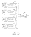
With reference to FIG. 2A, another conventional way for solving the problems of shadowing is shown. Four solar cell modules PV1-PV4 are connected in series as a solar cell array. Each solar cell module PV1-PV4 has two output terminals connected to a respective input terminal of a DC-DC power converter 41. Output terminals of the four DC-DC power converters 41 are connected in sequence and then further connected to input terminals of a power converter 42. Each DC-DC power converter 41 controls the output voltage of the respective solar cell module PV1-PV4. When any one of the solar cell modules PV1-PV4 is shaded, the shaded solar cell module can still provide partial output power to improve the total output power of the solar cell array.
With reference to FIG. 2B, each DC-DC power converter 41 needs two capacitors C1-C2, five power switches S1-S5, an inductor L and a diode D1. The capacitor C1 is parallel connected to the output of a solar cell module. The diode D1 is parallel connected to the output terminal of DC-DC power converter 41. If a solar cell array consists of n solar cell modules accompanied with DC-DC power converters, such large number of elements will cause the problems of high cost and complicated circuit connections.
The present invention thus develops a shadowing compensation device for a solar cell module to mitigate or solve the problems mentioned above.
SUMMARY OF THE INVENTION
The main objective of the present invention is to provide a shadowing compensation device with features of relatively simple circuit configuration, easy control and low cost for compensating a shaded solar cell module of a solar cell array, thereby increasing the total output voltage and the total output power of the solar cell array.
The shadowing compensation device comprises an input port, an output port and an isolated DC-DC power converter. The input port is for connecting to two output ends of the solar cell array. The output port is for connecting to one of the solar cell modules of the solar cell array. When the solar cell module connected to the output port has been shaded, the isolated DC-DC power converter draws a part of energy of the solar cell array and converts the energy to a compensation current for compensating the solar cell module being shaded. Therefore, the solar cell module being shaded is able to sustain its output voltage and continuously output power to ensure the total output voltage and the total output power of the solar cell array. In short, the present invention at least has the following advantages.
1. Because the shadowing compensation device is only connected to the solar cell module that will be shaded, not connected to all of the solar cell modules of the solar cell array, the circuit connection and circuit control are simplified, and high system reliability is obtained.
2. The conventional way for dealing with the problems of shadowing needs to manage the total output power of the solar cell array. In contrast with the conventional way, the shadowing compensation device of the present invention is only connected to the solar cell module that will be shaded. When the solar cell module is shaded, the shadowing compensation device only processes a relative small power of the shaded solar cell module, such that its manage power is reduced. Therefore, the power loss of the shadowing compensation device is reduced as much as possible.
3. The shadowing compensation device is operated only when the solar cell module is shaded. When there is no solar cell module being shaded, the non-operated shadowing compensation device will not affect the solar cell array to ensure a high power converting efficiency.
Other objectives, advantages and novel features of the invention will become more apparent from the following detailed description when taken in conjunction with the accompanying drawings.
BRIEF DESCRIPTION OF THE DRAWINGS
FIG. 1 shows a conventional voltage balancing circuit for a solar cell array;
FIG. 2A is a circuit block diagram showing a conventional way for solving the problems of shadowing;
FIG. 2B is a detailed circuit diagram of the DC-DC power converters in FIG. 2A;
FIG. 3 is a block circuit diagram of a shadowing compensation device in accordance with the present invention applied to a solar cell array;
FIG. 4 is a first embodiment of the shadowing compensation device in accordance with the present invention; and
FIG. 5 is a second embodiment of the shadowing compensation device in accordance with the present invention.
DETAILED DESCRIPTION OF THE PREFERRED EMBODIMENTS
With reference to FIG. 3, a shadowing compensation device 2 of the present invention is applied to a solar power generating system that includes a solar cell array 1 and a power converter 3. The shadowing compensation device 2 comprises an input port 20, an isolated DC-DC power converter 21, and an output port 22.
The solar cell array 1 comprises multiple solar cell modules 11-14 connected in series and forms two output ends. In this embodiment, the solar cell array 1 comprises four solar cell modules 11-14 of the same type. Thus, the output voltages and the output powers of the solar cell modules 11-14 are substantially equal to each other under the same environmental conditions. A sum of the four output voltages of the four solar cell modules 11-14 is defined as a total output voltage VT of the solar cell array 1 across the two output ends.
The input port 20 and output port 22 of the shadowing compensation device 2 have two connecting nodes respectively as shown in FIG. 3. The two connecting nodes of the input port 20 are connected to the two output ends of the solar cell array 1 respectively. Any one of the solar cell modules 11-14 may be shaded. For demonstration purpose, the solar cell module 14 is supposed to be completely or partially shaded. Therefore, the two connecting nodes of the output port 22 have to be connected across the two ends of the solar cell module 14. The power converter 3 may be a DC-DC power converter to control the total output voltage VT and perform a maximum power tracking to the solar cell array 1.
Still referring to FIG. 3, the shadowing compensation device 2 will not work as long as no solar cell module is shaded. Therefore, the shadowing compensation device 2 will not cause additional energy loss. When the solar cell module 14 is shaded, the shadowing compensation device 2 operates. The shaded solar cell module 14 will slightly change its maximum-power voltage VMPP, but will significantly reduce its maximum-power current IMPP. The extent of the reduction of the maximum-power current IMPP depends on the shaded degree of the solar cell module 14.
The shadowing compensation device 2 has a voltage gain 1/n, wherein “n” is the number of the solar cell modules of the solar cell array 1. For the solar cell array 1 shown in FIG. 3, n=4. With such a voltage gain, the output voltage of the shaded solar cell module 14 approximates the output voltage of each solar cell module 11-13 unshaded. By applying the shadowing compensation device 2 to the solar power generating system, the shadowing compensation device 2 supplies a compensation current ICOM to the shaded solar cell module 14. Therefore, the output voltage of the shaded solar cell module 14 can be maintained as close to its maximum-power voltage VMPP as possible. Thereby, the shaded solar cell module 14 remains at its regular output current for continuously supplying power.
If the solar power generating system works alone without using the shadowing compensation device 2 of the present invention, the following problems may occur. Since the output current of each unshaded solar cell module 11-13 operated at the maximum-power voltage is larger than the output current of the shaded solar cell module 14, a diode connected across the shaded solar cell module 14 is turned on to clamp the output voltage of the shaded solar cell module 14 to about 0 volt. The shaded solar cell module 14 stops supplying the output power. The total output voltage and the total output power of the solar cell array 1 are decreased. The P-V curve showing relationships between the maximum output power (P) and the total output voltage (V) of the solar cell array 1 will have multiple peak points. Multiple peak points increase difficulties in tracking the maximum output power.
However, the shadowing compensation device 2 of the present invention draws a part of energy from the two output ends of the solar cell array 1 to supply the compensation current ICOM to the shaded solar cell module 14. The compensation current ICOM is equal to a difference between the output current of the shaded solar cell module 14 and the output current of each unshaded solar cell module 11-13 operated at the maximum output power.
The shadowing compensation device 2 is operated only when the solar cell module 14 has been shaded. The shadowing compensation device 2 supplies a compensation power PCOM approximating to a product of the compensation current ICOM and one fourth of the total output voltage (VT) of the solar cell array 1, i.e. PCOM=(VT/4)×ICOM. The amount of the compensation power PCOM depends on the shaded degree of the solar cell module 14, but it is smaller than or equal to one fourth of the total output power of the solar cell array 1. Therefore, the shadowing compensation device 2 with a small capacity can be accomplished, and the manage power for solving the problems of shadowing is also small as compared with the conventional way where it needs to manage the total output power of the whole solar cell array 1. In contrast with the conventional way, using the shadowing compensation device 2 of the present invention can reduce power loss. Since the shadowing compensation device 2 will not operate until the solar cell module 14 is shaded, the efficiency of the solar cell array 1 is almost unaffected by the shadowing compensation device 2.
Because the shadowing compensation device 2 is only connected to the solar cell module 14 that will be shaded, and is not connected to all of the solar cell modules 11-14, the circuit connection and control can be simplified to obtain high system reliability.
In the situation that multiple solar cell modules will be shaded, multiple shadowing compensation devices 2 should be applied to these solar cell modules, respectively. The input port 20 of each shadowing compensation device 2 is connected to the two output ends of the solar cell array 1, and the output port 22 of each shadowing compensation device 2 is connected to the output terminals of the corresponding solar cell module that will be shaded.
With reference to FIG. 4, a first embodiment of the isolated DC-DC power converter 21 of the shadowing compensation device 2 is implemented by a flyback DC-DC power converter 21A. The flyback DC-DC power converter 21A comprises an input capacitor 2111, a transformer 2112 with two sides, a power switch 2113, a diode 2114 and an output capacitor 2115. The transformer 2112 transfers DC power from one side into the other side. The power switch 2113 is connected between the transformer 2112 and the input port 20. The diode 2114 is connected between the transformer 2112 and the output port (22). The input capacitor 2111 is connected to the input port 20, and the output capacitor 2115 is connected to the output port 22.
With reference to FIG. 5, a second embodiment of the isolated DC-DC power converter 21 of the shadowing compensation device 2 is implemented by a forward DC-DC power converter 21B. The forward DC-DC power converter 21B comprises an input capacitor 2121, a transformer 2122, a power switch 2123, a diode 2124, a diode 2125, an inductor 2126 and an output capacitor 2127. The input capacitor 2121 is connected to the input port 20, and the output capacitor 2127 is connected to the output port 22.
Even though numerous characteristics and advantages of the present invention have been set forth in the foregoing description, together with details of the structure and features of the invention, the disclosure is illustrative only. Changes may be made in the details, especially in matters of shape, size, and arrangement of parts within the principles of the invention to the full extent indicated by the broad general meaning of the terms in which the appended claims are expressed.

Claims (5)

What is claimed is:
1. A solar cell system with shadowing compensation comprising: a solar cell array comprising multiple solar cell modules connected in series to form two output ends, with the multiple solar cell modules comprising a single first solar cell module and multiple second solar cell modules; and a single shadowing compensation device only connected to the first solar cell module but not the multiple second cell modules comprising: an input port connecting to the two output ends of the solar cell array; an output port only connecting to the single first solar cell module of the solar cell array without connecting to the multiple second solar cell modules of the solar cell array; and an isolated DC-DC power converter, wherein the isolated DC-DC power converter outputs a compensation current to the single first solar cell module connected to the output port; wherein each of the second solar cell modules is not connected to any respective shadowing compensation device
wherein the compensation current is equal to a difference between an output current of the multiple second solar cell modules operated at a maximum output power and an output current of the first solar cell module.
2. The solar cell system as claimed in claim 1, wherein the isolated DC-DC power converter is a flyback DC-DC power converter.
3. The solar cell system as claimed in claim 1, wherein the isolated DC-DC power converter is a forward DC-DC power converter.
4. The solar cell system as claimed in claim 1, wherein the isolated DC-DC power converter is operated only when the single first solar cell module connected to the output port is completely or partially shaded.
5. A solar cell system with shadowing compensation comprising: a solar cell array comprising multiple solar cell modules connected in series to form two output ends, with the multiple solar cell modules comprising a single first solar cell module and multiple second solar cell modules; and a single shadowing compensation device only connected to the first solar cell module but not the multiple second cell modules comprising: an input port connecting to the two output ends of the solar cell array; an output port only connecting to the single first solar cell module of the solar cell array without connecting to the multiple second solar cell modules of the solar cell array; and an isolated DC-DC power converter, wherein the isolated DC-DC power converter outputs a compensation current to the single first solar cell module connected to the output port;
wherein the shadowing compensation device has a voltage gain 1/n, n is a total number of the first solar cell module and the second solar modules of the solar cell array, each of the second solar cell modules is not connected to any respective shadowing compensation device and
wherein the compensation current is equal to a difference between an output current of the multiple second solar cell modules operated at a maximum output power and an output current of the first solar cell module.
US14/072,875 2013-11-06 2013-11-06 Shadowing compensation device for solar cell module Active 2034-01-06 US9461581B2 (en)

Priority Applications (1)

Application Number Priority Date Filing Date Title
US14/072,875 US9461581B2 (en) 2013-11-06 2013-11-06 Shadowing compensation device for solar cell module

Applications Claiming Priority (1)

Application Number Priority Date Filing Date Title
US14/072,875 US9461581B2 (en) 2013-11-06 2013-11-06 Shadowing compensation device for solar cell module

Publications (2)

Publication Number Publication Date
US20150122312A1 US20150122312A1 (en) 2015-05-07
US9461581B2 true US9461581B2 (en) 2016-10-04

Family

ID=53006091

Family Applications (1)

Application Number Title Priority Date Filing Date
US14/072,875 Active 2034-01-06 US9461581B2 (en) 2013-11-06 2013-11-06 Shadowing compensation device for solar cell module

Country Status (1)

Country Link
US (1) US9461581B2 (en)

Families Citing this family (2)

* Cited by examiner, † Cited by third party
Publication number Priority date Publication date Assignee Title
US20180013377A1 (en) * 2016-07-11 2018-01-11 International Business Machines Corporation Mitigating the Effects on Shading in Photovoltaic Cells Using Flow Batteries
CN108258715B (en) * 2018-03-05 2022-01-14 南京南瑞继保电气有限公司 Inspection method and control device for bypass thyristor valve bank

Citations (6)

* Cited by examiner, † Cited by third party
Publication number Priority date Publication date Assignee Title
US20090303703A1 (en) * 2008-06-06 2009-12-10 Ching-Shang Kao Solar-Powered LED Street Light
US20100001587A1 (en) * 2008-07-01 2010-01-07 Satcon Technology Corporation Photovoltaic dc/dc micro-converter
US20110031816A1 (en) * 2009-07-30 2011-02-10 Nxp B.V. Photovoltaic unit, a dc-dc converter therefor, and a method of operating the same
US20120091800A1 (en) * 2011-10-28 2012-04-19 The Board Of Trustees Of The University Of Illinois System and Method for Optimizing Solar Power Conversion
US20120098344A1 (en) * 2009-05-08 2012-04-26 Nxp B.V. Photovoltaic units, methods of operating photovoltaic units and controllers therefor
CN103066888A (en) 2013-01-23 2013-04-24 浙江大学 Photovoltaic module with self compensating function

Patent Citations (6)

* Cited by examiner, † Cited by third party
Publication number Priority date Publication date Assignee Title
US20090303703A1 (en) * 2008-06-06 2009-12-10 Ching-Shang Kao Solar-Powered LED Street Light
US20100001587A1 (en) * 2008-07-01 2010-01-07 Satcon Technology Corporation Photovoltaic dc/dc micro-converter
US20120098344A1 (en) * 2009-05-08 2012-04-26 Nxp B.V. Photovoltaic units, methods of operating photovoltaic units and controllers therefor
US20110031816A1 (en) * 2009-07-30 2011-02-10 Nxp B.V. Photovoltaic unit, a dc-dc converter therefor, and a method of operating the same
US20120091800A1 (en) * 2011-10-28 2012-04-19 The Board Of Trustees Of The University Of Illinois System and Method for Optimizing Solar Power Conversion
CN103066888A (en) 2013-01-23 2013-04-24 浙江大学 Photovoltaic module with self compensating function

Also Published As

Publication number Publication date
US20150122312A1 (en) 2015-05-07

Similar Documents

Publication Publication Date Title
US6151234A (en) Apparatus for converting a direct current into an alternating current
US20180233919A1 (en) Photovoltaic inverter system and operation method thereof
EP3163734B1 (en) Dc-dc converter with high transformer ratio
US20150236589A1 (en) Power conditioner and method of controlling power conditioner
US20120153729A1 (en) Multi-input bidirectional dc-dc converter
US9024594B2 (en) System and method for power conversion for renewable energy sources
US20140152107A1 (en) Photovoltaic power generation system
CN101958658A (en) Be used for system, the method and apparatus of DC power transfer to AC power
US9059643B2 (en) Switching configuration and method for the production of an alternating voltage from at least supply terminals with temporally variable output DC voltage
US20190148947A1 (en) System and device for exporting power, and method of configuring thereof
US9461581B2 (en) Shadowing compensation device for solar cell module
US9948172B2 (en) Power converter for eliminating ripples
US9647570B2 (en) Photovoltaic system and method of operation
KR101034263B1 (en) DC-DC Convert for the Photovoltaic System
KR101412352B1 (en) Dc-dc convert
Bodele et al. Multi‐input battery‐integrated single‐stage DC‐DC converter for reliable operation of solar photovoltaic‐based systems
US20150295409A1 (en) Micro-grid operation system with smart energy management
US20150326108A1 (en) Dual source dc to dc converter
KR20160047131A (en) Three-phase inverter and power converting apparatus in generation system
KR101687913B1 (en) UPFC device with a single transformer
US20130134785A1 (en) Single stage power conversion system
KR20220164883A (en) Solar charging system for vehicle
CN104425646A (en) Solar-battery-module shielding-compensating device
US10305287B2 (en) Method for operating a photovoltaic system
US20140117755A1 (en) Power system

Legal Events

Date Code Title Description
AS Assignment

Owner name: ABLEREX ELECTRONICS CO., LTD., TAIWAN

Free format text: ASSIGNMENT OF ASSIGNORS INTEREST;ASSIGNORS:FENG, YA-TSUNG;SHEN, JIA-MIN;HOU, WEN-JIE;REEL/FRAME:031551/0583

Effective date: 20131106

STCF Information on status: patent grant

Free format text: PATENTED CASE

MAFP Maintenance fee payment

Free format text: PAYMENT OF MAINTENANCE FEE, 4TH YR, SMALL ENTITY (ORIGINAL EVENT CODE: M2551); ENTITY STATUS OF PATENT OWNER: SMALL ENTITY

Year of fee payment: 4

MAFP Maintenance fee payment

Free format text: PAYMENT OF MAINTENANCE FEE, 8TH YR, SMALL ENTITY (ORIGINAL EVENT CODE: M2552); ENTITY STATUS OF PATENT OWNER: SMALL ENTITY

Year of fee payment: 8