US9459226B2 - Lens coating/contamination electronic detection - Google Patents
Lens coating/contamination electronic detection Download PDFInfo
- Publication number
- US9459226B2 US9459226B2 US14/024,740 US201314024740A US9459226B2 US 9459226 B2 US9459226 B2 US 9459226B2 US 201314024740 A US201314024740 A US 201314024740A US 9459226 B2 US9459226 B2 US 9459226B2
- Authority
- US
- United States
- Prior art keywords
- capacitor
- value
- capacitor plate
- optical element
- gap
- Prior art date
- Legal status (The legal status is an assumption and is not a legal conclusion. Google has not performed a legal analysis and makes no representation as to the accuracy of the status listed.)
- Expired - Fee Related, expires
Links
Images


Classifications
-
- G—PHYSICS
- G01—MEASURING; TESTING
- G01N—INVESTIGATING OR ANALYSING MATERIALS BY DETERMINING THEIR CHEMICAL OR PHYSICAL PROPERTIES
- G01N27/00—Investigating or analysing materials by the use of electric, electrochemical, or magnetic means
- G01N27/02—Investigating or analysing materials by the use of electric, electrochemical, or magnetic means by investigating impedance
- G01N27/22—Investigating or analysing materials by the use of electric, electrochemical, or magnetic means by investigating impedance by investigating capacitance
- G01N27/24—Investigating the presence of flaws
-
- G—PHYSICS
- G01—MEASURING; TESTING
- G01N—INVESTIGATING OR ANALYSING MATERIALS BY DETERMINING THEIR CHEMICAL OR PHYSICAL PROPERTIES
- G01N27/00—Investigating or analysing materials by the use of electric, electrochemical, or magnetic means
- G01N27/02—Investigating or analysing materials by the use of electric, electrochemical, or magnetic means by investigating impedance
- G01N27/22—Investigating or analysing materials by the use of electric, electrochemical, or magnetic means by investigating impedance by investigating capacitance
-
- G—PHYSICS
- G01—MEASURING; TESTING
- G01N—INVESTIGATING OR ANALYSING MATERIALS BY DETERMINING THEIR CHEMICAL OR PHYSICAL PROPERTIES
- G01N21/00—Investigating or analysing materials by the use of optical means, i.e. using sub-millimetre waves, infrared, visible or ultraviolet light
- G01N21/01—Arrangements or apparatus for facilitating the optical investigation
- G01N21/15—Preventing contamination of the components of the optical system or obstruction of the light path
- G01N2021/155—Monitoring cleanness of window, lens, or other parts
-
- G—PHYSICS
- G01—MEASURING; TESTING
- G01N—INVESTIGATING OR ANALYSING MATERIALS BY DETERMINING THEIR CHEMICAL OR PHYSICAL PROPERTIES
- G01N21/00—Investigating or analysing materials by the use of optical means, i.e. using sub-millimetre waves, infrared, visible or ultraviolet light
- G01N21/17—Systems in which incident light is modified in accordance with the properties of the material investigated
- G01N21/55—Specular reflectivity
-
- G—PHYSICS
- G01—MEASURING; TESTING
- G01N—INVESTIGATING OR ANALYSING MATERIALS BY DETERMINING THEIR CHEMICAL OR PHYSICAL PROPERTIES
- G01N27/00—Investigating or analysing materials by the use of electric, electrochemical, or magnetic means
- G01N27/02—Investigating or analysing materials by the use of electric, electrochemical, or magnetic means by investigating impedance
- G01N27/04—Investigating or analysing materials by the use of electric, electrochemical, or magnetic means by investigating impedance by investigating resistance
- G01N27/20—Investigating the presence of flaws
Definitions
- the present invention generally relates to optical systems, and more particularly to detecting contamination within such optical systems.
- Optical metrology and inspection equipment such as, for example, reflectometers may often use high power optical lens/objectives in close proximity to surfaces for measurement and/or inspection purposes. In manufacturing environments these surfaces may often release gases or vapors that can coat the lens/objectives in such a manner that light collected by these lens/objectives is distorted and/or attenuated. The measurement and/or inspection results may thus be distorted as a result of the measurement being influenced by the existing contamination.
- contaminants e.g., gases/vapors
- equipment e.g., reflectometer systems, photolithographic systems
- a contamination detection apparatus may include an optical element having an outer surface and an other surface opposing the outer surface, a first capacitor plate located on the outer surface at an outer periphery of the optical element, and a second capacitor plate located on the outer surface at the outer periphery of the optical element.
- the second capacitor plate is located adjacent the first capacitor plate and separated from the first capacitor by a gap to form a capacitor, whereby a contaminant is electrically detected based on the contaminant entering the gap and varying a capacitance value corresponding to the capacitor.
- a method of determining contamination over an outer surface of a final stage optical element of an optical system may include applying an alternating signal having a predetermined voltage amplitude to a first capacitor plate located on the outer surface at an outer periphery of the optical element, and applying a ground signal to a second capacitor plate located on the outer surface at the outer periphery of the optical element, whereby the second capacitor plate is located adjacent the first capacitor plate and separated from the first capacitor by a gap to form a capacitor.
- An electrical current value associated with the capacitor is measured based on the applied alternating signal.
- a capacitive reactance value for the capacitor is then measured based on the measured current value and the applied predetermined voltage amplitude.
- a contaminant on the outer surface of the optical element is detected based on the calculated capacitive reactance, whereby the capacitive reactance varies based on the contaminant entering the gap.
- a computer program product for determining contamination over an outer surface of a final stage optical element of an optical system
- the computer program product may include a computer readable storage medium readable by a processing circuit and storing instructions for execution by the processing circuit for performing a method.
- the method may include measuring an alternating signal having a voltage amplitude that is applied between a first capacitor plate located on the outer surface at an outer periphery of the optical element and a second capacitor plate located on the outer surface at the outer periphery of the optical element.
- the second capacitor plate is located adjacent the first capacitor plate and separated from the first capacitor by a gap to form a capacitor.
- An electrical current value associated with the capacitor is measured based on the applied alternating signal.
- a resistance value is calculated based on the measured current value and the measured voltage amplitude.
- a contaminant on the outer surface of the optical element is then determined based on the calculated resistance value, whereby the resistance value varies based on the contaminant entering the gap.
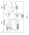
- FIG. 1A is an optical system, according to one embodiment
- FIG. 1B is an expanded cross sectional view of an optical element having an optical reflective device that is used as an optical reference within the optical system of FIG. 1A , according to one embodiment;
- FIG. 1C is a plan view of an outer surface of the optical element depicted in FIG. 1B , which shows a contamination detection capacitor, according to one embodiment
- FIG. 1D is a plan view of an inner surface of the optical element depicted in FIG. 1B , which shows a reference capacitor plate, according to one embodiment
- FIG. 2 is block diagram of an electronic contamination detection circuit used in the optical system of FIG. 1A , according to one embodiment
- FIG. 3 is a flow chart for an electronic contamination detection process corresponding to a final stage optical element within the optical system of FIG. 1A , according to one embodiment.
- FIG. 4 is a block diagram of hardware and software within the measurement processing unit of FIG. 1A , according to one embodiment.
- aspects of the present invention may be embodied as a system, method or computer program product. Accordingly, aspects of the present invention may take the form of an entirely hardware embodiment, an entirely software embodiment (including firmware, resident software, micro-code, etc.) or an embodiment combining software and hardware aspects that may all generally be referred to herein as a “circuit,” “module” or “system.” Furthermore, aspects of the present invention may take the form of a computer program product embodied in one or more computer readable medium(s) having computer readable program code embodied thereon.
- the computer readable medium may be a computer readable signal medium or a computer readable storage medium.
- a computer readable storage medium may be, for example, but not limited to, an electronic, magnetic, optical, electromagnetic, infrared, or semiconductor system, apparatus, or device, or any suitable combination of the foregoing.
- a computer readable storage medium may be any tangible medium that can contain, or store a program for use by or in connection with an instruction execution system, apparatus, or device.
- a computer readable signal medium may include a propagated data signal with computer readable program code embodied therein, for example, in baseband or as part of a carrier wave. Such a propagated signal may take any of a variety of forms, including, but not limited to, electro-magnetic, optical, or any suitable combination thereof.
- a computer readable signal medium may be any computer readable medium that is not a computer readable storage medium and that can communicate, propagate, or transport a program for use by or in connection with an instruction execution system, apparatus, or device.
- Program code embodied on a computer readable medium may be transmitted using any appropriate medium, including but not limited to wireless, wireline, optical fiber cable, RF, etc., or any suitable combination of the foregoing.
- Computer program code for carrying out operations for aspects of the present invention may be written in any combination of one or more programming languages, including an object oriented programming language such as Java, Smalltalk, C++ or the like and conventional procedural programming languages, such as the “C” programming language or similar programming languages.
- the program code may execute entirely on the user's computer, partly on the user's computer, as a stand-alone software package, partly on the user's computer and partly on a remote computer or entirely on the remote computer or server.
- the remote computer may be connected to the user's computer through any type of network, including a local area network (LAN) or a wide area network (WAN), or the connection may be made to an external computer (for example, through the Internet using an Internet Service Provider).
- LAN local area network
- WAN wide area network
- Internet Service Provider for example, AT&T, MCI, Sprint, EarthLink, MSN, GTE, etc.
- These computer program instructions may also be stored in a computer readable medium that can direct a computer, other programmable data processing apparatus, or other devices to function in a particular manner, such that the instructions stored in the computer readable medium produce an article of manufacture including instructions which implement the function/act specified in the flowchart and/or block diagram block or blocks.
- the computer program instructions may also be loaded onto a computer, other programmable data processing apparatus, or other devices to cause a series of operational steps to be performed on the computer, other programmable apparatus or other devices to produce a computer implemented process such that the instructions which execute on the computer or other programmable apparatus provide processes for implementing the functions/acts specified in the flowchart and/or block diagram block or blocks.
- the following one or more exemplary embodiments describe, among other things, an electronic surface contamination detection apparatus utilized within an optical system for determining measurement errors that may be caused by contaminants coating the one or more optical components of the optical system.
- the optical system 100 may include an optical source 102 , one or more optical elements 104 such as lenses, mirrors, splitters, etc., a collimating lens 106 , a first splitter 108 , a second splitter 110 , a final stage optical element 112 such as a focusing lens, a reference signal photodetector 114 , a surface reflected signal photodetector 116 , a photodetector focusing lens 118 , an electrical contamination detection circuit 121 , and a measurement processing unit 120 .
- the above-mentioned components 102 - 120 of the optical system 100 may be housed in a sealed and pressurized enclosure 122 in order to protect these optical components from debris (e.g., gases) that may impact the measurements.
- a focused incident optical signal I i illuminates a surface under test S, whereby a reflected portion (i.e., from surface S) I o , as indicated by 129 , of the focused incident optical signal I i is used to determine the reflectivity characteristics of the surface under test S.
- the surface under test S may include a film, dielectric, or any other layer associated with a device such as a manufactured semiconductor structure. By determining the reflectivity of such surfaces S, the characteristics and/or manufacturing tolerances of the films, dielectrics, or other layers may be determined.
- the optical source 102 e.g., arc lamp, incandescent lamp, fluorescent lamp, etc.
- the optical signal output from optical source 102 propagates along path 127 and is received by the one or more optical elements 104 such as lenses, mirrors, splitters, etc. As the optical signal traverses through the one or more optical elements 104 , it is received by collimating lens 106 .
- the incident optical signal is directed towards the beam splitter 108 (Path A), such that the beam splitter 108 reflects the collimated incident optical signal I i down onto the final stage optical element 112 (Path B), which may, for example, include a focusing lens.
- the final stage optical element 112 generates a focused incident optical signal I i at the surface under reflectivity test S (Path C).
- the surface under test S illuminated by the focused incident optical signal I i may then, based on its characteristic reflectivity (R), reflect anywhere between approximately all (total reflection) to approximately none (total absorption) of the focused incident optical signal I i at surface S back towards the final stage optical element 112 as a reflected optical signal I o (Path C).
- the final stage optical element 112 may then collimate the reflected optical signal I o from surface S back towards the beam splitter 108 (Path B).
- the reflected optical signal I o propagates through the beam splitter 108 (Path D) and onto beam splitter 110 .
- Beam splitter 110 subsequently directs reflected optical signal I o onto the photodetector focusing lens 118 (Path E) for focusing (Path F) onto the active area of the surface reflected signal photodetector 116 .
- the surface reflected signal photodetector 116 then converts the optical intensity of the reflected optical signal I o to a magnitude value (i.e., voltage or current value) that is determinative of the detected optical intensity (i.e., power).
- the magnitude value output from the photodetector 116 is then transmitted to the measurement unit 120 for processing.
- a portion of the incident optical signal is directed towards the beam splitter 108 (Path 1), such that the beam splitter 108 also reflects the portion of the incident optical signal I′ i down onto the final stage optical element 112 (Path 2), which may, for example, include a focusing lens.
- the final stage optical element 112 includes a reflective device 130 having a known reflective surface that reflects the portion of the incident optical signal I′ i back through the final stage optical element 112 and away from the surface under reflectivity test S (Path 3).
- the reflective surface of the reflective device 130 is set to provide maximum reflection, the reflective surface may include a high reflectivity material such as aluminum, silver, or gold with known reflectivity.
- Region 125 which includes the final stage optical element 112 and reflective device 130 , is further described below with the aid of an expanded view of region 125 , as depicted in FIG. 1B .
- the portion of the incident optical signal I′ i reflected back through the final stage optical element 112 by reflective device 130 is then received by the active area of the reference signal photodetector 114 .
- the reference signal photodetector 114 then converts the optical intensity of the portion of the incident optical signal I′ i to a magnitude value (i.e., voltage or current value) that is determinative of the detected optical intensity (i.e., power) based on the known reflectivity of reference device 130 .
- the magnitude value output from the photodetector 114 is then transmitted to the measurement unit 120 for processing.
- the portion of the incident optical signal I′ i detected by reference signal photodetector 114 acts a reference signal, whereby the ratio between the determined magnitude value corresponding to the reflected optical signal I o and the determined magnitude value corresponding to the portion of the incident optical signal I′ i provides the reflectivity (R) measure of the surface under test S.
- the portion of the incident optical signal I′ i detected by reference signal photodetector 114 may be a predetermined/known percentage (e.g., 10%) of the total optical signal that is output from the optical source 102 . Therefore, during the calibration of the optical system, this portion (i.e., 10%) of the incident optical signal I′ i detected by the reference signal photodetector 114 may be accordingly weighted (i.e., 90%) to be in proportion with incident optical signal I i that is applied to surface S.
- the weighting may be achieved by amplifying the output of photodetector 114 using known photoreceiver circuitry. In other implementations, the weighting may be achieved by the measurement processing unit 120 prior to calculating the reflectivity value (R).
- the reflectivity (R) measure of the surface under test S there may be a degree of uncertainty leading to a variation in power associated with the measured magnitude of the reflected optical signal I o and the measured magnitude of the portion of the incident optical signal I′ i .
- the measured magnitude of the reflected optical signal I o associated with surface S may deviate from its actual value.
- the measured magnitude of the portion of the incident optical signal I′ i serving as an optical reference signal may deviate from its actual value. Since the reflective device 130 is located at the last stage to reflect back the portion of the incident optical signal I′ i (the optical reference signal), it may be advantageous for the reflective device 130 to provide a reflective surface that is independent of any characteristic changes (e.g., loss) that could apply to the final stage optical element 112 .
- any deviations in optical power associated with the portion of incident optical signal I′ i may be attributed to any one of the components (i.e., 102 - 108 ) that are upstream from the final stage optical element 112 .
- a cross sectional view of the final stage optical element 112 depicts the reflective device 130 being integrated with the final stage optical element 112 in a manner that mitigates any contamination associated with the reflective device.
- the reflective device 130 provides a degree of measurement confidence that identifies any upstream fluctuations in power that results from the optical system components and not the reflectivity device 130 itself.
- reflective device 130 is formed on outer surface 156 of the final stage optical element 112 , whereby outer surface 156 faces the surface under test S.
- the reflective device 130 is also formed at a region offset X from the optical axis 135 of the final stage optical element 112 .
- the reflectivity device 130 includes a reflective surface layer 137 having top and bottom opposing surfaces 140 a , 140 b .
- the top surface 140 a of the reflective surface layer 137 is deposited on outer surface 156 of the final stage optical element 112 , such that top surface 140 a is encapsulated between surfaces 156 and 157 , while bottom surface 140 b of the reflective surface layer 137 remains exposed to the surface under test S.
- top surface 140 a Since the top surface 140 a is encapsulated between surfaces 156 and 157 , it is shielded from debris and contamination that may result from, for example, the surface under test S. Moreover, outer surface 156 of the final stage optical element 112 is enclosed in a sealed and/or pressurized enclosure. In contrast, the bottom surface 140 b of the reflective surface layer 137 that is exposed to the surface under test S may become contaminated by gases that may be released from surface S. This, however, does not affect the reflectivity of top surface 140 a , which as depicted, reflects the portion of the incident optical signal I′ i from the outer surface 156 of the final stage optical element 112 back through opposing surface 157 of the final stage optical element 112 .
- an exemplary embodiment of an electronic contamination detection system may be utilized to detect contamination on the outer surface of the final stage optical element 112 .
- the electronic contamination detection system i.e., FIGS. 1B-1D ) determines the measurement integrity of the optical system across the entire optical path leading to the illuminated surface.
- the outer surface 156 plan view of the final stage optical element 112 depicts capacitor plates 155 a , 155 b being formed on the outer periphery of the final stage optical element 112 .
- the capacitor plates 155 a , 155 b therefore create a capacitor for detecting debris or contamination on the outer surface of the optical element.
- the separation d between the capacitor plates 155 a , 155 b may, for example, be in the range of 0.5-2.0 millimeters (mm).
- the thickness t 1 , t 2 of the capacitor plates 155 a , 155 b may be, for example, 1 mm, while the height h of the capacitor plates 155 a , 155 b , as depicted by the A-A′ cross-section view, may be in the region of 2.0 mm.
- the height to thickness aspect ratio for the capacitor plates 155 a , 155 b should be no more than two (2) in order to avoid the capacitor plates 155 a , 155 b from breaking away from outer surface 156 of the final stage optical element 112 during, for example, cleaning processes. Larger aspect ratios may, however, be contemplated based on the type of cleaning and adhesion used to couple the capacitor plates 155 a , 155 b to the outer periphery of the final stage optical element 112 .
- the capacitor plates 155 a , 155 b , 155 c are depicted as elongate and extending circumferentially around the outer periphery of the optical element 112 , the plates may be any other shape and extend partially around the outer periphery of the optical element 112 .
- the capacitor plates 155 a , 155 b may, for example, be located at one or more regions of the outer surface 156 of the optical element 112 and be electrically coupled to generate an aggregate capacitance value (i.e., generating parallel capacitors).
- the separation d between the capacitor plates 155 a , 155 b is filled by air, whereby the electric constant ( ⁇ o ) for air is about 8.854 ⁇ 10 ⁇ 12 Fm ⁇ 1 .
- the capacitance (C) value is determined by:
- ⁇ o is the electric constant
- A is the surface area of each of the capacitor plates 155 a , 155 b
- d is the separation between the capacitor plates 155 a , 155 b .
- debris or a contaminant covers the outer surface 156 of the optical element 112 , the contaminant fills the gap g p separating the capacitor plates 155 a , 155 b by d.
- the relative static permittivity may vary between, for example, a factor of about 2 to 100.
- the capacitance value may vary between a factor of 2 to 100 when the outer surface 156 of the optical element 112 is covered by a contaminant.
- This change in capacitance (C) may, therefore, create enough sensitivity for an electrical contamination detection system 121 ( FIGS. 1A & 2 ) to determine the existence of the outer surface 156 contamination.
- the capacitor plates 155 a , 155 b may be formed from, for example, a silver material.
- the inner capacitor plate 155 a and the reflectivity device 130 may be integrated as a result of being formed from the same piece of silver.
- the optical element 112 may include a high numeric aperture lens having a diameter of about 20 mm and a working distance in the micrometer ( ⁇ m) range.
- a plan view corresponding to the other surface 157 of the final stage optical element 112 depicts capacitor plate 155 c being formed on the outer periphery of the final stage optical element 112 .
- surface 157 faces the internal optical elements of the system 100 ( FIG. 1A ), while outer surface 156 faces an external device or the surface S under test.
- the thickness t 3 of the capacitive plate 155 c may be, for example, 1 mm, while the height h of the capacitor plate 155 c , as depicted by the A-A′ cross-section view, may be in the region of 2.0 mm.
- capacitor plates 155 b and 155 c form a reference capacitor that may be utilized for evaluating the operation integrity of the electrical contamination detection system 121 ( FIGS. 1A & 2 ).
- the capacitance value of the reference capacitor formed by capacitor plate 155 b and 155 c remains at a fixed value regardless of whether the outer surface 156 of the optical element becomes covered with a contaminant.
- the electrical contamination detection system 121 FIGS. 1A & 2
- a change in capacitance value may generate a corresponding change in capacitive reactance given by:
- the electrical contamination detection system 121 depicted in FIG. 2 uses the changes in capacitive reactance value (X c ), which follows any changes in capacitance C, to determine the existence of a contaminant over the outer surface 156 ( FIG. 1C ) of the optical element 112 .
- the relative static permittivity ( ⁇ r ) may vary between, for example, a factor of about 2 to 100. This indicates that the capacitance C and, therefore, the capacitive reactance X c may vary between a factor of 2 to 100.
- one exemplary embodiment of the electrical contamination detection system 121 may include a signal generation source such as a signal generator 202 , an electrical current measurement device such as a current meter 204 , switch SW 1 , and switch SW 2 .
- the ground terminal 206 of the signal generator 202 may be electrically coupled to capacitor plate 155 b of the contamination detection capacitor (C CD ) 220 formed by capacitor plates 155 a and 155 b (also see FIG. 1C ).
- Terminal 208 of the signal generator 202 may be electrically coupled to input terminal 210 of the current meter 204 .
- Output terminal 212 of the current meter 204 couples to capacitor plate 155 a (also see FIG.
- the output terminal 212 of the current meter 204 also couples to capacitor plate 155 c of the reference capacitor (C R ) 225 formed by capacitor plates 155 b and 155 c (also see FIG. 1D ) via switch SW 2 .
- switch SW 2 may be periodically closed while SW 1 is opened.
- the signal generator 202 generates an alternating signal having a predetermined frequency (e.g., 1 MHz) and voltage value (e.g., 5V).
- the current meter 204 measures the current value (I r ) drawn by the reference capacitor (C R ) 225 based on its capacitive reactance.
- the current value remains constant at the different measurement periods based on the reference capacitor (C R ) 225 having a constant capacitance value.
- this current value (I r ) varies as a result of a change in capacitance value for the reference capacitor (C R ) 225 , it may be an indication of a circuit failure.
- switch SW 2 in a contamination detection mode of operation, switch SW 2 remains open while SW 1 is closed for continuous monitoring.
- the signal generator 202 generates an alternating signal having a predetermined frequency (e.g., 1 MHz) and voltage value (e.g., 5V).
- the current meter 204 measures the current value (I c ) drawn by the contamination detection capacitor (C CD ) 220 based on its capacitive reactance.
- the current value (I c ) is measured to be at a first value based on the contamination detection capacitor (C CD ) 220 having a capacitance and, therefore, a capacitive reactance that is based on a relative static permittivity ( ⁇ r ) of about one (1).
- the gap g p ( FIG. 1C ) between capacitor plates 155 a and 155 b may be almost entirely filled with air, which includes a relative static permittivity ( ⁇ r ) of about one (1).
- the gap g p ( FIG. 1C ) between capacitor plates 155 a and 155 b may almost entirely be filled with the contaminant, which includes a relative static permittivity ( ⁇ r ) ranging from, for example, 2-100.
- the capacitance (C) and, therefore, the capacitive reactance (X c ) may change by a factor of about 2-100 based on the variation in the relative static permittivity ( ⁇ r ).
- This change in the capacitance (C) and, therefore, the capacitive reactance (X c ) changes the current value (I c ) measured by the current meter 204 , which may be indicative of a contaminant covering the outer surface 156 ( FIG. 1C ) of the contamination detection capacitor (C CD ) 220 .
- the capacitive reactance (X c ) is magnified by a factor of about 2-100, the capacitive reactance (X c ) is accordingly reduced by a factor of about 2-100. This in turn may cause the current value (I c ) to increase by about 2-100 times, which will be measured by the current meter 204 .
- the current meter 204 measurements, and the predetermined frequency and voltage settings of the signal generator 202 are coupled to the measurement processing unit 120 ( FIG. 1A ) by the electrical contamination detection circuit 121 via communications link 123 ( FIG. 1A ).
- the communications link 123 may include either a wired or wireless link employing any suitable communication protocol and data communications format.
- an electrical contamination detection circuit may include any exemplary electrical circuit or device capable of generating electrical output changes as a function of variations in capacitance.
- an integrator circuit (not shown) employing an operational amplifier may be used to determine capacitance changes as a function of output rise time or fall time governed by the RC-time-constant of the integrator. Accordingly, the RC-time-constant may be measured and analyzed within measurement processing unit 120 ( FIG. 1A ) by sampling and digitizing the integrator output.
- the electrical contamination detection circuit 121 FIG. 1A
- the electrical contamination detection circuit 121 may be included, and thus, integrated within the measurement processing unit 120 ( FIG. 1A ).
- FIG. 3 is a flow chart 300 for an electronic contamination detection process corresponding to the outer surface of the final stage optical element 112 within the optical system of FIG. 1A , according to one embodiment.
- the process of flow chart 300 may be described with the aid of FIGS. 1A-1D and FIG. 2 .
- the process of flow chart 300 may be implemented as an executable program within measurement processing unit 120 ( FIG. 1A ).
- the process of flow chart 300 may, therefore, also be defined as electronic contamination detection process (ECDP) program 300 .
- ECDP electronic contamination detection process
- the measurement processing unit 120 receives the voltage (V) and frequency values (f) of a known alternating voltage (e.g., sinusoidal waveform) having a predetermined frequency that is applied to the contamination detection capacitor 220 (C CD ).
- the measurement processing unit 120 may set the voltage (V) and frequency values (f) of the known alternating voltage generated by the signal generator 202 , which is then applied to the contamination detection capacitor 220 (C CD ).
- the measurement processing unit 120 ( FIG. 1A ) may control the signal generator 202 via a control bus interface (not shown).
- the measurement processing unit 120 receives a measured current value (I c ) from the current meter 204 of the electrical contamination detection circuit 121 .
- the capacitive reactance X c of the contamination detection capacitor 220 (C CD ) is determined.
- a reference capacitive reactance X rc for the contamination detection capacitor 220 (C CD ) is retrieved based on measuring the capacitive reactance of the contamination detection capacitor 220 (C CD ) when the optical element 112 is contaminant free.
- the capacitive reactance X c of the contamination detection capacitor 220 (C CD ) is compared against the reference capacitive reactance X rc of the contamination detection capacitor 220 (C CD ) using the relationship of Equation (2). If the reference capacitive reactance X rc value exceeds the measured capacitive reactance X c value by a predetermined amount (e.g., X rc >X c , or X rc >X c +predetermined value), this may be indicative of the outer surface of the 156 of the optical element 112 being covered by a contaminant material.
- a predetermined amount e.g., X rc >X c , or X rc >X c +predetermined value
- the capacitive reactance X c value reduces based on the relative static permittivity ( ⁇ r ) increasing.
- the integrity of the electrical contamination detection circuit 121 is checked by monitoring the capacitive reactance value of the reference capacitor (C R ) 225 .
- This integrity may be evaluated by ensuring that the capacitive reactance value of the reference capacitor (C R ) 225 has remained substantially constant and the same as the capacitive reactance value obtained for the reference capacitor (C R ) 225 during the error-free operation of the electrical contamination detection circuit 121 .
- the operational integrity of the electrical contamination detection circuit 121 may need to be evaluated ( 314 ). However, if at 312 it is determined that the capacitive reactance value of the reference capacitor (C R ) 225 has not changed, at 316 a cleaning process for the optical element 112 may be initiated.
- the process returns to 302 and the contamination monitoring process continues.
- the relative static permittivity ( ⁇ r ) and, thus, the type of contaminant may be determined. Specifically, since the capacitive reactance X c is measured, using the known values of f, d, and A, the ⁇ r value may be calculated.
- the process of flow chart 300 may determine the existence of outer surface contaminant coatings using resistance value calculations in place of capacitive reactance. For example, the known or measured alternating voltage V value (i.e., amplitude) and the measured current I value may be used, based on the V/R relation, to determine a resistance value ( 306 ). Thus, for example, step 310 may determine whether a retrieved ( 308 ) predetermined reference resistance value (R R ) exceeds the determined resistance value (R) based on driving the contamination detection capacitor (C CD ) with an alternating signal.
- FIG. 4 shows a block diagram of the components of a data processing system 800 , 900 , such as measurement processing unit 120 ( FIG. 1A ) in accordance with an illustrative embodiment of the present invention. It should be appreciated that FIG. 4 provides only an illustration of one implementation and does not imply any limitations with regard to the environments in which different embodiments may be implemented. Many modifications to the depicted environments may be made based on design and implementation requirements.
- Data processing system 800 , 900 is representative of any electronic device capable of executing machine-readable program instructions.
- Data processing system 800 , 900 may be representative of a smart phone, a computer system, PDA, or other electronic devices.
- Examples of computing systems, environments, and/or configurations that may represented by data processing system 800 , 900 include, but are not limited to, personal computer systems, server computer systems, thin clients, thick clients, hand-held or laptop devices, multiprocessor systems, microprocessor-based systems, network PCs, minicomputer systems, and distributed cloud computing environments that include any of the above systems or devices.
- Measurement processing unit 120 may include respective sets of internal components 800 a, b, c and external components 900 a, b, c illustrated in FIG. 4 .
- Each of the sets of internal components 800 a, b, c includes one or more processors 820 , one or more computer-readable RAMs 822 and one or more computer-readable ROMs 824 on one or more buses 826 , and one or more operating systems 828 and one or more computer-readable tangible storage devices 830 .
- the one or more operating systems 828 and programs such as the ECDP program 300 corresponding to measurement processing unit 120 ( FIG.
- each of the computer-readable tangible storage devices 830 is a magnetic disk storage device of an internal hard drive.
- each of the computer-readable tangible storage devices 830 is a semiconductor storage device such as ROM 824 , EPROM, flash memory or any other computer-readable tangible storage device that can store a computer program and digital information.
- Each set of internal components 800 a, b, c also includes a R/W drive or interface 832 to read from and write to one or more portable computer-readable tangible storage devices 936 such as a CD-ROM, DVD, memory stick, magnetic tape, magnetic disk, optical disk or semiconductor storage device.
- the optical system processing program 300 ( FIG. 3 ) associated with measurement processing unit 120 ( FIG. 1A ) can be stored on one or more of the respective portable computer-readable tangible storage devices 936 , read via the respective R/W drive or interface 832 and loaded into the respective hard drive 830 .
- Each set of internal components 800 a, b, c may also include network adapters (or switch port cards) or interfaces 836 such as a TCP/IP adapter cards, wireless wi-fi interface cards, or 3G or 4G wireless interface cards or other wired or wireless communication links.
- Optical system processing program 300 ( FIG. 3 ), in measurement processing unit 120 ( FIG. 1A ), can be downloaded to measurement processing unit 120 ( FIG. 1A ) from an external computer (e.g., server) via a network (for example, the Internet, a local area network or other, wide area network) and respective network adapters or interfaces 836 . From the network adapters (or switch port adaptors) or interfaces 836 , the optical system processing program 300 ( FIG. 3 ) associated with measurement processing unit 120 ( FIG. 1A ) is loaded into the respective hard drive 830 .
- the network may comprise copper wires, optical fibers, wireless transmission, routers, firewalls, switches, gateway computers and/or edge servers.
- Each of the sets of external components 900 a, b, c can include a computer display monitor 920 , a keyboard 930 , and a computer mouse 934 .
- External components 900 a, b, c can also include touch screens, virtual keyboards, touch pads, pointing devices, and other human interface devices.
- Each of the sets of internal components 800 a, b, c also includes device drivers 840 to interface to computer display monitor 920 , keyboard 930 and computer mouse 934 .
- the device drivers 840 , R/W drive or interface 832 and network adapter or interface 836 comprise hardware and software (stored in storage device 830 and/or ROM 824 ).
- the aforementioned programs can be written in any combination of one or more programming languages, including low-level, high-level, object-oriented or non object-oriented languages, such as Java, Smalltalk, C, and C++.
- the program code may execute entirely on the user's computer, partly on the user's computer, as a stand-alone software package, partly on the user's computer and partly on a remote computer, or entirely on a remote computer or server.
- the remote computer may be connected to the user's computer through any type of network, including a local area network (LAN) or a wide area network (WAN), or the connection may be made to an external computer (for example, through the Internet using an Internet service provider).
- LAN local area network
- WAN wide area network
- the functions of the aforementioned programs can be implemented in whole or in part by computer circuits and other hardware (not shown).
- each block in the flowchart or block diagrams may represent a module, segment, or portion of code, which comprises one or more executable instructions for implementing the specified logical function(s).
- the functions noted in the block may occur out of the order noted in the figures. For example, two blocks shown in succession may, in fact, be executed substantially concurrently, or the blocks may sometimes be executed in the reverse order, depending upon the functionality involved.
Landscapes
- Chemical & Material Sciences (AREA)
- Chemical Kinetics & Catalysis (AREA)
- Electrochemistry (AREA)
- Physics & Mathematics (AREA)
- Health & Medical Sciences (AREA)
- Life Sciences & Earth Sciences (AREA)
- Analytical Chemistry (AREA)
- Biochemistry (AREA)
- General Health & Medical Sciences (AREA)
- General Physics & Mathematics (AREA)
- Immunology (AREA)
- Pathology (AREA)
- Investigating Or Analysing Materials By Optical Means (AREA)
Abstract
Description
Claims (17)
Priority Applications (1)
| Application Number | Priority Date | Filing Date | Title |
|---|---|---|---|
| US14/024,740 US9459226B2 (en) | 2013-09-12 | 2013-09-12 | Lens coating/contamination electronic detection |
Applications Claiming Priority (1)
| Application Number | Priority Date | Filing Date | Title |
|---|---|---|---|
| US14/024,740 US9459226B2 (en) | 2013-09-12 | 2013-09-12 | Lens coating/contamination electronic detection |
Publications (2)
| Publication Number | Publication Date |
|---|---|
| US20150070032A1 US20150070032A1 (en) | 2015-03-12 |
| US9459226B2 true US9459226B2 (en) | 2016-10-04 |
Family
ID=52624988
Family Applications (1)
| Application Number | Title | Priority Date | Filing Date |
|---|---|---|---|
| US14/024,740 Expired - Fee Related US9459226B2 (en) | 2013-09-12 | 2013-09-12 | Lens coating/contamination electronic detection |
Country Status (1)
| Country | Link |
|---|---|
| US (1) | US9459226B2 (en) |
Cited By (1)
| Publication number | Priority date | Publication date | Assignee | Title |
|---|---|---|---|---|
| US20240195950A1 (en) * | 2020-11-06 | 2024-06-13 | Waymo Llc | Localized Window Contaminant Detection |
Families Citing this family (1)
| Publication number | Priority date | Publication date | Assignee | Title |
|---|---|---|---|---|
| US10302585B2 (en) * | 2016-01-07 | 2019-05-28 | Apple Inc. | Capacitive DOE integrity monitor |
Citations (1)
| Publication number | Priority date | Publication date | Assignee | Title |
|---|---|---|---|---|
| GB2185578A (en) * | 1985-12-24 | 1987-07-22 | Land Infrared Ltd | Optical temperature transducers |
-
2013
- 2013-09-12 US US14/024,740 patent/US9459226B2/en not_active Expired - Fee Related
Patent Citations (1)
| Publication number | Priority date | Publication date | Assignee | Title |
|---|---|---|---|---|
| GB2185578A (en) * | 1985-12-24 | 1987-07-22 | Land Infrared Ltd | Optical temperature transducers |
Cited By (2)
| Publication number | Priority date | Publication date | Assignee | Title |
|---|---|---|---|---|
| US20240195950A1 (en) * | 2020-11-06 | 2024-06-13 | Waymo Llc | Localized Window Contaminant Detection |
| US12445594B2 (en) * | 2020-11-06 | 2025-10-14 | Waymo Llc | Localized window contaminant detection |
Also Published As
| Publication number | Publication date |
|---|---|
| US20150070032A1 (en) | 2015-03-12 |
Similar Documents
| Publication | Publication Date | Title |
|---|---|---|
| KR102214716B1 (en) | Apparatus for measuring thickness of thin film, measuring system comprising the same, and method for measuring thickness of thin film | |
| TWI516746B (en) | Method, device and computer program product for performing anharmonic cycle error compensation in an interference coding system, and lithography system | |
| Mayerhöfer et al. | Removing interference-based effects from the infrared transflectance spectra of thin films on metallic substrates: a fast and wave optics conform solution | |
| Chiang et al. | Effects of temperature on the surface plasmon resonance at a metal–semiconductor interface | |
| JP7259813B2 (en) | Gas analysis system and gas analysis method | |
| JP2023551818A (en) | Surface topography measurement device and method | |
| CN105066889A (en) | A portable thin film thickness measuring device and a film thickness measuring method thereof | |
| US9459226B2 (en) | Lens coating/contamination electronic detection | |
| CN107991728A (en) | Broadband and wide visual field angle compensator | |
| KR102320292B1 (en) | Defect inspection method for phase shift mask and defect inspection apparatus for same | |
| CN102830048A (en) | Wafer Particle Inspection Method | |
| CN112001900B (en) | Ultraviolet environment steel structure coating detection method, device, server and storage medium | |
| Knollenberg | The importance of media refractive index in evaluating liquid and surface microcontamination measurements | |
| CN114199527B (en) | OD value detection method, system and storage medium of graded optical filter | |
| US9116038B2 (en) | Integrated optical illumination reference source | |
| JP2011196766A (en) | Method for measuring shape of measured object having light transmittance | |
| KR20210076813A (en) | Global dynamic detection method and system for protective film of photomask | |
| US7369235B1 (en) | Method and system for measuring deep trenches in silicon | |
| CN114868257B (en) | Hybrid sensor including plasmon resonator | |
| JP3802028B2 (en) | Protective relay using photocurrent sensor | |
| US20070015295A1 (en) | Methods and systems for characterizing semiconductor materials | |
| EP1907789A1 (en) | Methods and systems for characterizing semiconductor materials | |
| Grezes-Besset et al. | Absorbing coating in magnetron sputtering for parasitic light reduction | |
| Cheng et al. | Combining cubic spline interpolation and fast Fourier transform to extend measuring range of reflectometry | |
| US11366059B2 (en) | System and method to measure refractive index at specific wavelengths |
Legal Events
| Date | Code | Title | Description |
|---|---|---|---|
| AS | Assignment |
Owner name: INTERNATIONAL BUSINESS MACHINES CORPORATION, NEW Y Free format text: ASSIGNMENT OF ASSIGNORS INTEREST;ASSIGNOR:STROCCHIA-RIVERA, CARLOS;REEL/FRAME:031190/0635 Effective date: 20130912 |
|
| AS | Assignment |
Owner name: GLOBALFOUNDRIES U.S. 2 LLC, NEW YORK Free format text: ASSIGNMENT OF ASSIGNORS INTEREST;ASSIGNOR:INTERNATIONAL BUSINESS MACHINES CORPORATION;REEL/FRAME:036550/0001 Effective date: 20150629 |
|
| AS | Assignment |
Owner name: GLOBALFOUNDRIES INC., CAYMAN ISLANDS Free format text: ASSIGNMENT OF ASSIGNORS INTEREST;ASSIGNORS:GLOBALFOUNDRIES U.S. 2 LLC;GLOBALFOUNDRIES U.S. INC.;REEL/FRAME:036779/0001 Effective date: 20150910 |
|
| STCF | Information on status: patent grant |
Free format text: PATENTED CASE |
|
| AS | Assignment |
Owner name: WILMINGTON TRUST, NATIONAL ASSOCIATION, DELAWARE Free format text: SECURITY AGREEMENT;ASSIGNOR:GLOBALFOUNDRIES INC.;REEL/FRAME:049490/0001 Effective date: 20181127 |
|
| FEPP | Fee payment procedure |
Free format text: MAINTENANCE FEE REMINDER MAILED (ORIGINAL EVENT CODE: REM.); ENTITY STATUS OF PATENT OWNER: LARGE ENTITY |
|
| LAPS | Lapse for failure to pay maintenance fees |
Free format text: PATENT EXPIRED FOR FAILURE TO PAY MAINTENANCE FEES (ORIGINAL EVENT CODE: EXP.); ENTITY STATUS OF PATENT OWNER: LARGE ENTITY |
|
| STCH | Information on status: patent discontinuation |
Free format text: PATENT EXPIRED DUE TO NONPAYMENT OF MAINTENANCE FEES UNDER 37 CFR 1.362 |
|
| AS | Assignment |
Owner name: GLOBALFOUNDRIES INC., CAYMAN ISLANDS Free format text: RELEASE BY SECURED PARTY;ASSIGNOR:WILMINGTON TRUST, NATIONAL ASSOCIATION;REEL/FRAME:054636/0001 Effective date: 20201117 |
|
| FP | Lapsed due to failure to pay maintenance fee |
Effective date: 20201004 |
|
| AS | Assignment |
Owner name: GLOBALFOUNDRIES U.S. INC., NEW YORK Free format text: RELEASE BY SECURED PARTY;ASSIGNOR:WILMINGTON TRUST, NATIONAL ASSOCIATION;REEL/FRAME:056987/0001 Effective date: 20201117 Owner name: GLOBALFOUNDRIES U.S. INC., NEW YORK Free format text: RELEASE OF SECURITY INTEREST;ASSIGNOR:WILMINGTON TRUST, NATIONAL ASSOCIATION;REEL/FRAME:056987/0001 Effective date: 20201117 |