US9449882B1 - Semiconductor device and manufacturing method thereof - Google Patents

Semiconductor device and manufacturing method thereof Download PDF

Info

Publication number
US9449882B1
US9449882B1 US14/927,190 US201514927190A US9449882B1 US 9449882 B1 US9449882 B1 US 9449882B1 US 201514927190 A US201514927190 A US 201514927190A US 9449882 B1 US9449882 B1 US 9449882B1
Authority
US
United States
Prior art keywords
layer
semiconductor layer
semiconductor
fin structure
fin
Prior art date
Legal status (The legal status is an assumption and is not a legal conclusion. Google has not performed a legal analysis and makes no representation as to the accuracy of the status listed.)
Expired - Fee Related
Application number
US14/927,190
Inventor
Sheng-Chen Wang
Kai-Hsuan LEE
Sai-Hooi Yeong
Chia-Ta Yu
Current Assignee (The listed assignees may be inaccurate. Google has not performed a legal analysis and makes no representation or warranty as to the accuracy of the list.)
Taiwan Semiconductor Manufacturing Co TSMC Ltd
Original Assignee
Taiwan Semiconductor Manufacturing Co TSMC Ltd
Priority date (The priority date is an assumption and is not a legal conclusion. Google has not performed a legal analysis and makes no representation as to the accuracy of the date listed.)
Filing date
Publication date
Application filed by Taiwan Semiconductor Manufacturing Co TSMC Ltd filed Critical Taiwan Semiconductor Manufacturing Co TSMC Ltd
Priority to US14/927,190 priority Critical patent/US9449882B1/en
Assigned to TAIWAN SEMICONDUCTOR MANUFACTURING CO., LTD. reassignment TAIWAN SEMICONDUCTOR MANUFACTURING CO., LTD. ASSIGNMENT OF ASSIGNORS INTEREST (SEE DOCUMENT FOR DETAILS). Assignors: LEE, KAI-HSUAN, WANG, SHENG-CHEN, YEONG, SAI-HOOI, YU, CHIA-TA
Priority to TW105124581A priority patent/TWI611459B/en
Priority to US15/242,155 priority patent/US10163728B2/en
Priority to DE102016117473.4A priority patent/DE102016117473A1/en
Publication of US9449882B1 publication Critical patent/US9449882B1/en
Application granted granted Critical
Priority to KR1020160135693A priority patent/KR20170051269A/en
Priority to CN201610907124.7A priority patent/CN106992154B/en
Priority to KR1020180127512A priority patent/KR101946765B1/en
Expired - Fee Related legal-status Critical Current
Anticipated expiration legal-status Critical

Links

Images

Classifications

    • H01L21/823431
    • HELECTRICITY
    • H10SEMICONDUCTOR DEVICES; ELECTRIC SOLID-STATE DEVICES NOT OTHERWISE PROVIDED FOR
    • H10DINORGANIC ELECTRIC SEMICONDUCTOR DEVICES
    • H10D30/00Field-effect transistors [FET]
    • H10D30/60Insulated-gate field-effect transistors [IGFET]
    • H10D30/611Insulated-gate field-effect transistors [IGFET] having multiple independently-addressable gate electrodes influencing the same channel
    • H01L21/823412
    • H01L27/0886
    • H01L29/165
    • H01L29/66795
    • HELECTRICITY
    • H10SEMICONDUCTOR DEVICES; ELECTRIC SOLID-STATE DEVICES NOT OTHERWISE PROVIDED FOR
    • H10DINORGANIC ELECTRIC SEMICONDUCTOR DEVICES
    • H10D30/00Field-effect transistors [FET]
    • H10D30/01Manufacture or treatment
    • H10D30/021Manufacture or treatment of FETs having insulated gates [IGFET]
    • H10D30/024Manufacture or treatment of FETs having insulated gates [IGFET] of fin field-effect transistors [FinFET]
    • HELECTRICITY
    • H10SEMICONDUCTOR DEVICES; ELECTRIC SOLID-STATE DEVICES NOT OTHERWISE PROVIDED FOR
    • H10DINORGANIC ELECTRIC SEMICONDUCTOR DEVICES
    • H10D30/00Field-effect transistors [FET]
    • H10D30/60Insulated-gate field-effect transistors [IGFET]
    • H10D30/62Fin field-effect transistors [FinFET]
    • H10D30/6215Fin field-effect transistors [FinFET] having multiple independently-addressable gate electrodes
    • HELECTRICITY
    • H10SEMICONDUCTOR DEVICES; ELECTRIC SOLID-STATE DEVICES NOT OTHERWISE PROVIDED FOR
    • H10DINORGANIC ELECTRIC SEMICONDUCTOR DEVICES
    • H10D30/00Field-effect transistors [FET]
    • H10D30/60Insulated-gate field-effect transistors [IGFET]
    • H10D30/62Fin field-effect transistors [FinFET]
    • H10D30/6219Fin field-effect transistors [FinFET] characterised by the source or drain electrodes
    • HELECTRICITY
    • H10SEMICONDUCTOR DEVICES; ELECTRIC SOLID-STATE DEVICES NOT OTHERWISE PROVIDED FOR
    • H10DINORGANIC ELECTRIC SEMICONDUCTOR DEVICES
    • H10D30/00Field-effect transistors [FET]
    • H10D30/60Insulated-gate field-effect transistors [IGFET]
    • H10D30/751Insulated-gate field-effect transistors [IGFET] having composition variations in the channel regions
    • HELECTRICITY
    • H10SEMICONDUCTOR DEVICES; ELECTRIC SOLID-STATE DEVICES NOT OTHERWISE PROVIDED FOR
    • H10DINORGANIC ELECTRIC SEMICONDUCTOR DEVICES
    • H10D30/00Field-effect transistors [FET]
    • H10D30/60Insulated-gate field-effect transistors [IGFET]
    • H10D30/791Arrangements for exerting mechanical stress on the crystal lattice of the channel regions
    • H10D30/797Arrangements for exerting mechanical stress on the crystal lattice of the channel regions being in source or drain regions, e.g. SiGe source or drain
    • HELECTRICITY
    • H10SEMICONDUCTOR DEVICES; ELECTRIC SOLID-STATE DEVICES NOT OTHERWISE PROVIDED FOR
    • H10DINORGANIC ELECTRIC SEMICONDUCTOR DEVICES
    • H10D62/00Semiconductor bodies, or regions thereof, of devices having potential barriers
    • H10D62/10Shapes, relative sizes or dispositions of the regions of the semiconductor bodies; Shapes of the semiconductor bodies
    • H10D62/17Semiconductor regions connected to electrodes not carrying current to be rectified, amplified or switched, e.g. channel regions
    • H10D62/351Substrate regions of field-effect devices
    • H10D62/357Substrate regions of field-effect devices of FETs
    • H10D62/364Substrate regions of field-effect devices of FETs of IGFETs
    • H10D62/371Inactive supplementary semiconductor regions, e.g. for preventing punch-through, improving capacity effect or leakage current
    • HELECTRICITY
    • H10SEMICONDUCTOR DEVICES; ELECTRIC SOLID-STATE DEVICES NOT OTHERWISE PROVIDED FOR
    • H10DINORGANIC ELECTRIC SEMICONDUCTOR DEVICES
    • H10D62/00Semiconductor bodies, or regions thereof, of devices having potential barriers
    • H10D62/80Semiconductor bodies, or regions thereof, of devices having potential barriers characterised by the materials
    • H10D62/82Heterojunctions
    • H10D62/822Heterojunctions comprising only Group IV materials heterojunctions, e.g. Si/Ge heterojunctions
    • HELECTRICITY
    • H10SEMICONDUCTOR DEVICES; ELECTRIC SOLID-STATE DEVICES NOT OTHERWISE PROVIDED FOR
    • H10DINORGANIC ELECTRIC SEMICONDUCTOR DEVICES
    • H10D62/00Semiconductor bodies, or regions thereof, of devices having potential barriers
    • H10D62/80Semiconductor bodies, or regions thereof, of devices having potential barriers characterised by the materials
    • H10D62/83Semiconductor bodies, or regions thereof, of devices having potential barriers characterised by the materials being Group IV materials, e.g. B-doped Si or undoped Ge
    • H10D62/832Semiconductor bodies, or regions thereof, of devices having potential barriers characterised by the materials being Group IV materials, e.g. B-doped Si or undoped Ge being Group IV materials comprising two or more elements, e.g. SiGe
    • HELECTRICITY
    • H10SEMICONDUCTOR DEVICES; ELECTRIC SOLID-STATE DEVICES NOT OTHERWISE PROVIDED FOR
    • H10DINORGANIC ELECTRIC SEMICONDUCTOR DEVICES
    • H10D84/00Integrated devices formed in or on semiconductor substrates that comprise only semiconducting layers, e.g. on Si wafers or on GaAs-on-Si wafers
    • H10D84/01Manufacture or treatment
    • H10D84/0123Integrating together multiple components covered by H10D12/00 or H10D30/00, e.g. integrating multiple IGBTs
    • H10D84/0126Integrating together multiple components covered by H10D12/00 or H10D30/00, e.g. integrating multiple IGBTs the components including insulated gates, e.g. IGFETs
    • H10D84/0128Manufacturing their channels
    • HELECTRICITY
    • H10SEMICONDUCTOR DEVICES; ELECTRIC SOLID-STATE DEVICES NOT OTHERWISE PROVIDED FOR
    • H10DINORGANIC ELECTRIC SEMICONDUCTOR DEVICES
    • H10D84/00Integrated devices formed in or on semiconductor substrates that comprise only semiconducting layers, e.g. on Si wafers or on GaAs-on-Si wafers
    • H10D84/01Manufacture or treatment
    • H10D84/0123Integrating together multiple components covered by H10D12/00 or H10D30/00, e.g. integrating multiple IGBTs
    • H10D84/0126Integrating together multiple components covered by H10D12/00 or H10D30/00, e.g. integrating multiple IGBTs the components including insulated gates, e.g. IGFETs
    • H10D84/0158Integrating together multiple components covered by H10D12/00 or H10D30/00, e.g. integrating multiple IGBTs the components including insulated gates, e.g. IGFETs the components including FinFETs
    • HELECTRICITY
    • H10SEMICONDUCTOR DEVICES; ELECTRIC SOLID-STATE DEVICES NOT OTHERWISE PROVIDED FOR
    • H10DINORGANIC ELECTRIC SEMICONDUCTOR DEVICES
    • H10D84/00Integrated devices formed in or on semiconductor substrates that comprise only semiconducting layers, e.g. on Si wafers or on GaAs-on-Si wafers
    • H10D84/01Manufacture or treatment
    • H10D84/0123Integrating together multiple components covered by H10D12/00 or H10D30/00, e.g. integrating multiple IGBTs
    • H10D84/0126Integrating together multiple components covered by H10D12/00 or H10D30/00, e.g. integrating multiple IGBTs the components including insulated gates, e.g. IGFETs
    • H10D84/0165Integrating together multiple components covered by H10D12/00 or H10D30/00, e.g. integrating multiple IGBTs the components including insulated gates, e.g. IGFETs the components including complementary IGFETs, e.g. CMOS devices
    • H10D84/0167Manufacturing their channels
    • HELECTRICITY
    • H10SEMICONDUCTOR DEVICES; ELECTRIC SOLID-STATE DEVICES NOT OTHERWISE PROVIDED FOR
    • H10DINORGANIC ELECTRIC SEMICONDUCTOR DEVICES
    • H10D84/00Integrated devices formed in or on semiconductor substrates that comprise only semiconducting layers, e.g. on Si wafers or on GaAs-on-Si wafers
    • H10D84/01Manufacture or treatment
    • H10D84/0123Integrating together multiple components covered by H10D12/00 or H10D30/00, e.g. integrating multiple IGBTs
    • H10D84/0126Integrating together multiple components covered by H10D12/00 or H10D30/00, e.g. integrating multiple IGBTs the components including insulated gates, e.g. IGFETs
    • H10D84/0165Integrating together multiple components covered by H10D12/00 or H10D30/00, e.g. integrating multiple IGBTs the components including insulated gates, e.g. IGFETs the components including complementary IGFETs, e.g. CMOS devices
    • H10D84/0188Manufacturing their isolation regions
    • HELECTRICITY
    • H10SEMICONDUCTOR DEVICES; ELECTRIC SOLID-STATE DEVICES NOT OTHERWISE PROVIDED FOR
    • H10DINORGANIC ELECTRIC SEMICONDUCTOR DEVICES
    • H10D84/00Integrated devices formed in or on semiconductor substrates that comprise only semiconducting layers, e.g. on Si wafers or on GaAs-on-Si wafers
    • H10D84/01Manufacture or treatment
    • H10D84/0123Integrating together multiple components covered by H10D12/00 or H10D30/00, e.g. integrating multiple IGBTs
    • H10D84/0126Integrating together multiple components covered by H10D12/00 or H10D30/00, e.g. integrating multiple IGBTs the components including insulated gates, e.g. IGFETs
    • H10D84/0165Integrating together multiple components covered by H10D12/00 or H10D30/00, e.g. integrating multiple IGBTs the components including insulated gates, e.g. IGFETs the components including complementary IGFETs, e.g. CMOS devices
    • H10D84/0193Integrating together multiple components covered by H10D12/00 or H10D30/00, e.g. integrating multiple IGBTs the components including insulated gates, e.g. IGFETs the components including complementary IGFETs, e.g. CMOS devices the components including FinFETs
    • HELECTRICITY
    • H10SEMICONDUCTOR DEVICES; ELECTRIC SOLID-STATE DEVICES NOT OTHERWISE PROVIDED FOR
    • H10DINORGANIC ELECTRIC SEMICONDUCTOR DEVICES
    • H10D84/00Integrated devices formed in or on semiconductor substrates that comprise only semiconducting layers, e.g. on Si wafers or on GaAs-on-Si wafers
    • H10D84/01Manufacture or treatment
    • H10D84/02Manufacture or treatment characterised by using material-based technologies
    • H10D84/03Manufacture or treatment characterised by using material-based technologies using Group IV technology, e.g. silicon technology or silicon-carbide [SiC] technology
    • H10D84/038Manufacture or treatment characterised by using material-based technologies using Group IV technology, e.g. silicon technology or silicon-carbide [SiC] technology using silicon technology, e.g. SiGe
    • HELECTRICITY
    • H10SEMICONDUCTOR DEVICES; ELECTRIC SOLID-STATE DEVICES NOT OTHERWISE PROVIDED FOR
    • H10DINORGANIC ELECTRIC SEMICONDUCTOR DEVICES
    • H10D84/00Integrated devices formed in or on semiconductor substrates that comprise only semiconducting layers, e.g. on Si wafers or on GaAs-on-Si wafers
    • H10D84/80Integrated devices formed in or on semiconductor substrates that comprise only semiconducting layers, e.g. on Si wafers or on GaAs-on-Si wafers characterised by the integration of at least one component covered by groups H10D12/00 or H10D30/00, e.g. integration of IGFETs
    • H10D84/82Integrated devices formed in or on semiconductor substrates that comprise only semiconducting layers, e.g. on Si wafers or on GaAs-on-Si wafers characterised by the integration of at least one component covered by groups H10D12/00 or H10D30/00, e.g. integration of IGFETs of only field-effect components
    • H10D84/83Integrated devices formed in or on semiconductor substrates that comprise only semiconducting layers, e.g. on Si wafers or on GaAs-on-Si wafers characterised by the integration of at least one component covered by groups H10D12/00 or H10D30/00, e.g. integration of IGFETs of only field-effect components of only insulated-gate FETs [IGFET]
    • H10D84/834Integrated devices formed in or on semiconductor substrates that comprise only semiconducting layers, e.g. on Si wafers or on GaAs-on-Si wafers characterised by the integration of at least one component covered by groups H10D12/00 or H10D30/00, e.g. integration of IGFETs of only field-effect components of only insulated-gate FETs [IGFET] comprising FinFETs
    • HELECTRICITY
    • H10SEMICONDUCTOR DEVICES; ELECTRIC SOLID-STATE DEVICES NOT OTHERWISE PROVIDED FOR
    • H10DINORGANIC ELECTRIC SEMICONDUCTOR DEVICES
    • H10D84/00Integrated devices formed in or on semiconductor substrates that comprise only semiconducting layers, e.g. on Si wafers or on GaAs-on-Si wafers
    • H10D84/80Integrated devices formed in or on semiconductor substrates that comprise only semiconducting layers, e.g. on Si wafers or on GaAs-on-Si wafers characterised by the integration of at least one component covered by groups H10D12/00 or H10D30/00, e.g. integration of IGFETs
    • H10D84/82Integrated devices formed in or on semiconductor substrates that comprise only semiconducting layers, e.g. on Si wafers or on GaAs-on-Si wafers characterised by the integration of at least one component covered by groups H10D12/00 or H10D30/00, e.g. integration of IGFETs of only field-effect components
    • H10D84/83Integrated devices formed in or on semiconductor substrates that comprise only semiconducting layers, e.g. on Si wafers or on GaAs-on-Si wafers characterised by the integration of at least one component covered by groups H10D12/00 or H10D30/00, e.g. integration of IGFETs of only field-effect components of only insulated-gate FETs [IGFET]
    • H10D84/85Complementary IGFETs, e.g. CMOS
    • H10D84/853Complementary IGFETs, e.g. CMOS comprising FinFETs
    • HELECTRICITY
    • H10SEMICONDUCTOR DEVICES; ELECTRIC SOLID-STATE DEVICES NOT OTHERWISE PROVIDED FOR
    • H10PGENERIC PROCESSES OR APPARATUS FOR THE MANUFACTURE OR TREATMENT OF DEVICES COVERED BY CLASS H10
    • H10P14/00Formation of materials, e.g. in the shape of layers or pillars
    • H10P14/60Formation of materials, e.g. in the shape of layers or pillars of insulating materials
    • H10P14/63Formation of materials, e.g. in the shape of layers or pillars of insulating materials characterised by the formation processes
    • H10P14/6326Deposition processes
    • H10P14/6328Deposition from the gas or vapour phase
    • H10P14/6334Deposition from the gas or vapour phase using decomposition or reaction of gaseous or vapour phase compounds, i.e. chemical vapour deposition
    • HELECTRICITY
    • H10SEMICONDUCTOR DEVICES; ELECTRIC SOLID-STATE DEVICES NOT OTHERWISE PROVIDED FOR
    • H10PGENERIC PROCESSES OR APPARATUS FOR THE MANUFACTURE OR TREATMENT OF DEVICES COVERED BY CLASS H10
    • H10P14/00Formation of materials, e.g. in the shape of layers or pillars
    • H10P14/60Formation of materials, e.g. in the shape of layers or pillars of insulating materials
    • H10P14/69Inorganic materials
    • H10P14/694Inorganic materials composed of nitrides
    • H10P14/6943Inorganic materials composed of nitrides containing silicon
    • H10P14/69433Inorganic materials composed of nitrides containing silicon the material being a silicon nitride not containing oxygen, e.g. SixNy or SixByNz
    • HELECTRICITY
    • H10SEMICONDUCTOR DEVICES; ELECTRIC SOLID-STATE DEVICES NOT OTHERWISE PROVIDED FOR
    • H10WGENERIC PACKAGES, INTERCONNECTIONS, CONNECTORS OR OTHER CONSTRUCTIONAL DETAILS OF DEVICES COVERED BY CLASS H10
    • H10W10/00Isolation regions in semiconductor bodies between components of integrated devices
    • H10W10/01Manufacture or treatment
    • H10W10/011Manufacture or treatment of isolation regions comprising dielectric materials
    • H10W10/014Manufacture or treatment of isolation regions comprising dielectric materials using trench refilling with dielectric materials, e.g. shallow trench isolations
    • HELECTRICITY
    • H10SEMICONDUCTOR DEVICES; ELECTRIC SOLID-STATE DEVICES NOT OTHERWISE PROVIDED FOR
    • H10WGENERIC PACKAGES, INTERCONNECTIONS, CONNECTORS OR OTHER CONSTRUCTIONAL DETAILS OF DEVICES COVERED BY CLASS H10
    • H10W10/00Isolation regions in semiconductor bodies between components of integrated devices
    • H10W10/10Isolation regions comprising dielectric materials
    • H10W10/17Isolation regions comprising dielectric materials formed using trench refilling with dielectric materials, e.g. shallow trench isolations

Definitions

  • the disclosure relates to a semiconductor integrated circuit, and more particularly to a semiconductor device having a fin structure and its manufacturing process.
  • Fin FET devices typically include semiconductor fins with high aspect ratios and in which channel and source/drain regions of semiconductor transistor devices are formed.
  • a gate is formed over and along the sides of the fin structure (e.g., wrapping) utilizing the advantage of the increased surface area of the channel and source/drain regions to produce faster, more reliable and better-controlled semiconductor transistor devices.
  • germanium or silicon germanium (SiGe) may be used as a channel region to enhance carrier mobility.
  • FIGS. 1-12 are exemplary cross sectional views illustrating a sequential process for manufacturing a semiconductor FET device according to one embodiment of the present disclosure.
  • FIG. 13 is an exemplary perspective view corresponding to FIG. 12 .
  • FIGS. 14A and 14B are exemplary cross sectional views of source/drain structures.
  • FIGS. 15 and 16 are cross sectional views illustrating a sequential process for manufacturing a semiconductor FET device according to a modified embodiment of the present disclosure.
  • FIGS. 17-24 are exemplary cross sectional views illustrating a sequential process for manufacturing a semiconductor FET device according to another embodiment of the present disclosure.
  • first and second features are formed in direct contact
  • additional features may be formed interposing the first and second features, such that the first and second features may not be in direct contact.
  • Various features may be arbitrarily drawn in different scales for simplicity and clarity.
  • spatially relative terms such as “beneath,” “below,” “lower,” “above,” “upper” and the like, may be used herein for ease of description to describe one element or feature's relationship to another element(s) or feature(s) as illustrated in the figures.
  • the spatially relative terms are intended to encompass different orientations of the device in use or operation in addition to the orientation depicted in the figures.
  • the apparatus may be otherwise oriented (rotated 90 degrees or at other orientations) and the spatially relative descriptors used herein may likewise be interpreted accordingly.
  • the term “made of” may mean either “comprising” or “consisting of.”
  • FIGS. 1-10 are exemplary cross sectional views illustrating a sequential process for manufacturing a semiconductor FET device according to one embodiment of the present disclosure. It is understood that additional operations can be provided before, during, and after operations shown by FIGS. 1-10 , and some of the operations described below can be replaced or eliminated, for additional embodiments of the method. The order of the operations may be interchangeable.
  • a substrate 100 is provided and a first semiconductor layer 110 is formed over the substrate 100 . Further, second semiconductor layer 120 is formed over the first semiconductor layer.
  • the substrate 100 is, for example, a p-type silicon substrate with an impurity concentration in a range of about 1 ⁇ 10 15 cm ⁇ 3 and about 1 ⁇ 10 16 cm ⁇ 3 .
  • the substrate 100 is an n-type silicon substrate with an impurity concentration in a range of about 1 ⁇ 10 15 cm ⁇ 3 and about 1 ⁇ 10 16 cm ⁇ 3 .
  • the substrate 100 may comprise another elementary semiconductor, such as germanium; a compound semiconductor including IV-IV compound semiconductors such as SiC and SiGe, III-V compound semiconductors such as GaAs, GaP, GaN, InP, InAs, InSb, GaAsP, AlGaN, AlInAs, AlGaAs, GaInAs, GaInP, and/or GaInAsP; or combinations thereof.
  • the substrate 100 is a silicon layer of an SOI (silicon-on insulator) substrate. When an SOI substrate is used, the fin structure may protrude from the silicon layer of the SOI substrate or may protrude from the insulator layer of the SOI substrate.
  • the silicon layer of the SOI substrate is used to form the fin structure.
  • the substrate 100 may include various regions that have been suitably doped with impurities (e.g., p-type or n-type conductivity).
  • the dopants are, for example boron (BF 2 ), phosphorus and/or arsenic.
  • the substrate is a silicon substrate (wafer).
  • a first semiconductor layer 110 is epitaxially grown over the surface of the substrate 100
  • a second semiconductor layer 120 is epitaxially grown over the first semiconductor layer 110
  • a mask layer including a first layer 130 and a second layer 140 is formed over the second semiconductor layer 120 .
  • the first semiconductor layer 110 is, for example Si (1-x) Ge x , where x is in a range of about 0.1 to about 0.5. In some embodiments, x in Si (1-x) Ge x may be in a range of about 0.2 to about 0.4. In the present disclosure, Si (1-x) Ge x may be simply referred to as SiGe.
  • the thickness of the SiGe first semiconductor layer 110 is in a range of about 0.5 ⁇ m to about 2 ⁇ m in some embodiments.
  • the thickness of the SiGe first semiconductor layer 110 is in a range of about 1 ⁇ m to about 1.5 ⁇ m.
  • a Ge layer or a Si (1-x) Ge x where x is less than about 0.1, may be used as the first semiconductor layer 110 .
  • III-V compound semiconductors such as GaAs, GaP, GaN, InP, InAs, InSb, GaAsP, AlGaN, AlInAs, AlGaAs, GaInAs, GaInP, and/or GaInAsP may be used as the first semiconductor layer 110 .
  • the first semiconductor layer 110 may be doped or may not be doped.
  • the doping may be performed during the epitaxial growth of the first semiconductor layer 110 or may be performed by ion implantation.
  • the second semiconductor layer 120 is, for example Si or Si (1-y) Ge y , where y is less than about 0.1. In this embodiment, the second semiconductor layer is epitaxially grown Si.
  • the second semiconductor layer 120 has a thickness in a range of about 30 nm to about 200 nm in some embodiments. In certain embodiments, the thickness of the second semiconductor layer 120 is in a range of about 50 nm to about 150 nm.
  • the mask layer may include, for example, a pad oxide (e.g., silicon oxide) layer 130 and a silicon nitride (SiN) mask layer 140 in some embodiments.
  • the thickness of the pad oxide layer is in a range of about 2 nm to about 15 nm and the thickness of the silicon nitride mask layer is in a range of about 10 nm to about 50 nm in some embodiments.
  • the stacked layers of the first and second semiconductor layers are patterned into fin structures.
  • the mask layer is patterned into mask patterns 150 .
  • the width of each of the patterns 150 is in a range of about 5 nm to about 40 nm in some embodiments, or may be in a range of about 10 nm to about 30 nm in other embodiments.
  • the first and second semiconductor layers are pattered into fin structures 10 and 20 by trench etching using a dry etching method and/or a wet etching method. As shown in FIG. 2 , the trench etching is performed through the second semiconductor layer 120 and to the middle of the first semiconductor layer 110 .
  • the bottom portion of the fin structures 110 A are made of the first semiconductor layer, and the upper portion of the fin structures 120 are made of the second semiconductor layer.
  • the fin structure 10 is for a p-type Fin FET and the fin structure 20 is for an n-type Fin FET.
  • the fin structures 10 and 20 are disposed adjacent to each other, the fin structure 10 for a p-type Fin FET may be disposed apart from the fin structure 20 for an n-type Fin FET.
  • the number of the fin structures is not limited to one (or two). The numbers may be two or more.
  • one or more dummy fin structures may be disposed adjacent to both sides of the fin structure 10 and/or the fin structure 20 to improve pattern fidelity in patterning processes.
  • the fin structures 10 and 20 extend in the Y direction and arranged in the X direction crossing the Y direction.
  • the width of the fin structures 10 and 20 is in a range of about 5 nm to about 40 nm in some embodiments, and may be in a range of about 7 nm to about 15 nm in certain embodiments.
  • the height H 1 of the fin structures 10 and 20 is in a range of about 50 nm to about 300 nm in some embodiments, and may be in a range of about 100 nm to 200 nm in other embodiments.
  • the space between adjacent fin structures is in a range of about 5 nm to about 80 nm in some embodiments, and may be in a range of about 7 nm to 15 nm in other embodiments.
  • the remaining thickness H 2 of the first semiconductor layer 110 is in a range of about 500 ⁇ m to about 800 ⁇ m.
  • the height H 1 from the bottoms of the fin structure may be measured from the plane that corresponds to the average levels of the bottoms of the fin structures.
  • H 2 can be measured from the upper surface of the substrate 100 to the plane.
  • the fin structures 10 and 20 may have a tapered shape, in which the top width is smaller than the bottom width, in some embodiments. If the width of the fin structures 10 and 20 is not uniform from the top to the bottom, the width may be defined as an average width, a width at the vertical midpoint or a width at the interface between the first and second semiconductor layers.
  • the dimensions and values recited throughout the descriptions are merely examples, and may be changed to suit different scales of integrated circuits.
  • a protective (cover) layer 160 is formed to cover the fin structures 10 and 20 , as shown in FIG. 3 .
  • the protective layer 160 is made of a material that prevents an underlying layer (the first semiconductor layer) from being oxidized.
  • the protective layer 160 is made of one or more layers of silicon nitride (SiN), SiC, SiOCN and SiCN.
  • the thickness of the protective layer 160 is in a range of about 1 nm to about 10 nm in some embodiments. In certain embodiments, the thickness of the protective layers 160 is in a range of about 2 nm to about 5 nm in some embodiments. In this embodiment, SiN is used as the protective layers 160 .
  • the protective layer 160 is formed by chemical vapor deposition CVD, plasma-enhanced chemical vapor deposition (PECVD), atmospheric pressure chemical vapor deposition (APCVD), low-pressure CVD (LPCVD), high density plasma CVD (HDPCVD) and/or atomic layer deposition (ALD), and/or other suitable processes.
  • PECVD plasma-enhanced chemical vapor deposition
  • APCVD atmospheric pressure chemical vapor deposition
  • LPCVD low-pressure CVD
  • HDPCVD high density plasma CVD
  • ALD atomic layer deposition
  • the substrate temperature is in a range of 300° C. to 500° C. In some embodiments, the substrate temperature may be in a range of 350° C. to 450° C.
  • PECVD is utilized.
  • a sacrificial layer 170 is formed so that the fin structures 10 and 20 are embedded in the sacrificial layer 170 , as shown in FIG. 4 .
  • the fin structures 10 and 20 may be fully or partially embedded in the sacrificial layer 170 .
  • the sacrificial layer 170 is made of an organic material such as a photo resist layer or a material for a bottom antireflective coating (BARC).
  • the thickness of the sacrificial layer 170 is reduced by, for example, an etch-back process so as to expose a part of the fin structures.
  • the etch-back process may be performed by using plasma including O 2 and at least one of CF 4 and CHF 3 , at a temperature in a range about 0° C. to about 300° C. and at a pressure in a range of about 1 to about 10 Torr in certain embodiments.
  • etching time By adjusting etching time, a desired thickness of the remaining sacrificial layer can be obtained.
  • the thickness H 3 is adjusted to be greater than the height of the interface between the first semiconductor layer 110 A and the second semiconductor layer 120 by an amount D 1 .
  • the distance D 1 is in a range of about 5 nm to about 60 nm, or may be in a range of about 20 nm to 50 nm in other embodiments.
  • etching-back the thick sacrificial layer it may be possible to form a thin sacrificial layer having the target thickness directly by adjusting, for example, the film forming condition.
  • the upper portions of the protective layer 160 exposed from the sacrificial layer 170 are removed by, for example, dry etching and/or wet etching.
  • the hard mask patterns 150 may also be removed in this process.
  • the remaining sacrificial layer 170 is removed by, for example, an ashing process and/or a wet cleaning process.
  • isolation insulating layer 180 is formed.
  • the isolation insulating layer 180 is made of one or more layers of, for example, silicon dioxide, SiO, SiON, SiOCN or fluorine-doped silicate glass (FSG), or any other suitable dielectric material.
  • FSG fluorine-doped silicate glass
  • the isolation insulating layer 180 is made of silicon oxide, the silicon oxide may be doped with, for example, boron and/or phosphorous.
  • the isolation insulating layer 180 may be formed by a flowable CVD (FCVD).
  • FCVD flowable CVD
  • flowable dielectric materials instead of silicon oxide are deposited.
  • Flowable dielectric materials can “flow” during deposition to fill gaps or spaces with a high aspect ratio.
  • various chemistries are added to silicon-containing precursors to allow the deposited film to flow.
  • nitrogen hydride bonds are added.
  • flowable dielectric precursors particularly flowable silicon oxide precursors
  • examples of flowable dielectric precursors include a silicate, a siloxane, a methyl silsesquioxane (MSQ), a hydrogen silsesquioxane (HSQ), an MSQ/HSQ, a perhydrosilazane (TCPS), a perhydro-polysilazane (PSZ), a tetraethyl orthosilicate (TEOS), or a silyl-amine, such as trisilylamine (TSA).
  • silicate a siloxane
  • MSQ methyl silsesquioxane
  • HSQ hydrogen silsesquioxane
  • MSQ/HSQ an MSQ/HSQ
  • TCPS perhydrosilazane
  • PSZ perhydro-polysilazane
  • TEOS tetraethyl orthosilicate
  • TSA trisilylamine
  • the flowable film After the flowable film is deposited, it is cured and then annealed to remove undesired element(s) to form silicon oxide. When the undesired element(s) is removed, the flowable film densifies and shrinks. In some embodiments, multiple anneal processes are conducted. The flowable film is cured and annealed more than once.
  • the temperatures for annealing are also adjusted to relatively lower temperatures, such as in a range from about 500° C. to about 800° C.
  • relatively lower temperatures such as in a range from about 500° C. to about 800° C.
  • the bottom portion 110 A of the fin structures 10 and 20 are not oxidized during the thermal process for forming the isolation insulating layer 180 .
  • the upper portions of the isolation insulating layers 180 and the mask patterns 150 are removed by, for example, a chemical mechanical polishing (CMP) method or other planarization methods such as an etch-back process.
  • CMP chemical mechanical polishing
  • the top portions of the upper layers 120 of the fin structures may be slightly etched.
  • a protection hard mask layer 200 for example, a single layer of silicon nitride (in a range of about 10 nm to about 50 nm in some embodiments) or a bilayer of silicon nitride (in a range of about 10 nm to about 50 nm in some embodiments) and silicon oxide (in a range of about 5 nm to 50 nm in some embodiments), is formed over the isolation insulating layer 180 above the fin structure 20 for the n-type Fin FET region.
  • the protection hard mask layer 200 protects the fin structure 20 from the subsequent processes performed on the fin structure 10 for the p-type Fin FET.
  • the upper portion made by the second semiconductor layer 120 of the fin structure 10 is partially removed, thereby forming an opening 190 and a remaining second semiconductor layer 125 .
  • the etching of the second semiconductor layer 120 may be performed by dry etching and/or wet etching.
  • the thickness D 2 of the remaining second semiconductor layer 125 is in a range of about 5 nm to about 50 nm in some embodiments, or may be in a range of about 5 nm to about 25 nm in other embodiments. By adjusting the etching time and/or conditions, the desired thickness of the remaining second semiconductor layer 125 can be obtained.
  • the distance D 3 between the upper end of the protective layer 160 and the upper surface of the remaining second semiconductor layer 125 is in a range of about 5 nm to about 20 nm in some embodiments, or may be in a range of about 5 nm to about 10 nm in other embodiments.
  • a third semiconductor layer 210 is epitaxially grown on the upper surface of the remaining second semiconductor layer 125 so as to fill the opening 190 , as shown in FIG. 10 .
  • the third semiconductor layer may be Ge or a Si (1-z) Ge z , where z is larger than x of the first semiconductor layer 110 (Si (1-x) Ge x ). In some embodiments, z is equal to or more than about 0.5, and may be in a range of about 0.5 to about 0.75 in other embodiments.
  • the third semiconductor layer 210 is also formed above the upper surface of the isolation insulating layer 180 .
  • the protection hard mask layer 200 and part of the third semiconductor layer 210 formed above the upper surface of the isolation insulating layer 180 are removed by, for example, a planarization operation such as a CMP.
  • the upper portion of the isolation insulating layer 180 is removed (recessed) by, for example, an etch-back process, so that the upper portion of the second semiconductor layer 120 and the upper portion of the third semiconductor layer 210 are exposed from the isolation insulating layer 180 .
  • the isolation insulating layer 180 is recessed to the extent that the upper surface of the isolation insulating layer 180 becomes substantially the same height as the upper ends of the protective layer 160 .
  • the etch-back process may be performed by using dry etching or wet etching. By adjusting etching time, a desired thickness of the remaining isolation insulating layer 180 can be obtained.
  • the upper surface of the isolation insulating layer 180 may be located below the upper ends of the protective layer 160 , or above the upper ends of the protective layer 160 .
  • the exposed upper portion of the second semiconductor layer 120 becomes a channel region 120 A for the n-type Fin FET and the exposed upper portion of the third semiconductor layer 210 becomes a channel region 210 A for the p-type Fin FET.
  • the height D 4 of the exposed upper portions is in a range of about 20 nm to about 80 nm in some embodiments, and may be in a range of about 30 nm to about 60 nm in other embodiments.
  • the remaining second semiconductor layer 125 is not exposed from the isolation insulating layer 180 , and the bottom of the channel regions are embedded in the isolation insulating layer 180 .
  • a gate structure is formed over part of the channel regions 120 A and 210 A.
  • a gate dielectric material and a gate electrode material are formed over the isolation insulating layer 180 and the channel regions 120 A and 210 A, and then patterning operations are performed so as to obtain gate structure including the gate electrode layer 230 and the gate dielectric layer 220 .
  • the gate electrode layer 230 is made of one or more conductive material such as poly silicon, Al, Cu, W, Ti, Ta, TiN, TiAl, TiAlN, TaN, NiSi, CoSi, other conductive materials.
  • the electrode layer for the gate electrode layer 230 may be formed using a suitable process such as ALD, CVD, PVD, plating, or combinations thereof.
  • the gate dielectric layer 220 includes one or more layers of silicon oxide, silicon nitride, silicon oxy-nitride, or high-k dielectrics.
  • High-k dielectrics may include metal oxides. Examples of metal oxides used for high-k dielectrics include oxides of Li, Be, Mg, Ca, Sr, Sc, Y, Zr, Hf, Al, La, Ce, Pr, Nd, Sm, Eu, Gd, Tb, Dy, Ho, Er, Tm, Yb, Lu, and/or mixtures thereof.
  • high-k dielectric material examples include HfO 2 , HfSiO, HfSiON, HfTaO, HfSiO, HfZrO, zirconium oxide, aluminum oxide, titanium oxide, hafnium dioxide-alumina (HfO 2 —Al 2 O 3 ) alloy, other suitable high-k dielectric materials, and/or combinations thereof.
  • the gate dielectric layer 220 may be formed using a suitable operation such as atomic layer deposition (ALD), chemical vapor deposition (CVD), physical vapor deposition (PVD), thermal oxidation, UV-ozone oxidation, or combinations thereof.
  • the gate dielectric layer 220 may further include an interfacial layer (not shown) to reduce damage between the gate dielectric layer 220 and the channel regions.
  • the interfacial layer may include silicon oxide.
  • one or more work function adjustment layers may be interposed between the gate dielectric layer 220 and the gate electrode layer 230 .
  • the work function adjustment layer may include a single layer or alternatively a multi-layer structure, such as various combinations of a metal layer with a selected work function to enhance the device performance (work function metal layer), liner layer, wetting layer, adhesion layer, metal alloy or metal silicide.
  • the work function adjustment layer may alternatively include a polysilicon layer.
  • the work function adjustment layer may be formed by ALD, PVD, CVD, e-beam evaporation, or other suitable operation. Further, the work function adjustment layer may be formed separately for the n-channel Fin FET and the p-channel Fin FET, which may use different metal layers.
  • one gate structure is disposed for the n-type Fin FET and the p-type Fin FET.
  • the gate structure may be separately disposed for the n-type Fin FET and the p-type Fin FET, respectively.
  • FIG. 13 is an exemplary perspective view corresponding to FIG. 12 , illustrating one of Fin FETs of FIG. 12 .
  • source and drain 240 are formed.
  • the source and drain 240 may be formed by forming silicide layers on the upper portions of the fin structure not covered by the gate structure in some embodiments.
  • the upper portions of the fin structure not covered by the gate structure is recessed below the upper surface of the isolation insulating layer 180 , and a strain material is re-grown over the recessed fin structure.
  • the strain material may include one or more layers of Si, SiC, SiCP, SiP, SiCP, SiGe or Ge.
  • FIGS. 14A and 14B are exemplary cross sectional views of source/drain structures.
  • the remaining second semiconductor layer 125 (made of e.g., Si) is disposed between the first semiconductor layer 110 and the channel region 210 A in the p-type Fin FET.
  • the remaining second semiconductor layer 125 (made of e.g., Si) is disposed between the first semiconductor layer 110 (made of e.g., for example Si (1-x) Ge x , where x is in a range of about 0.1 to about 0.5) and the channel region 210 A (made of, for example, for example Ge or a Si (1-z) Ge z , where z is larger than x of the first semiconductor layer 110 (Si (1-x) Ge x )), it is possible to suppress Ge diffusion between the first semiconductor layer 110 and the channel region 210 A. In addition, by reducing annealing temperature for the isolation insulating layer 180 , the Ge diffusion can be further suppressed.
  • the remaining second semiconductor layer 125 may contain Ge in an amount of about 10 atm % or less. In other embodiments, the Ge amount in the remaining second semiconductor layer 125 may be less than about 5 atm %.
  • the Fin FET device may undergo further CMOS processes to form various features such as contacts/vias, interconnect metal layers, dielectric layers, passivation layers, etc.
  • FIGS. 15 and 16 are cross sectional views illustrating a sequential process for manufacturing a semiconductor FET device according to a modified embodiment of the present disclosure.
  • the second semiconductor layer 120 for the p-type Fin FET is partially etched and the bottom part of the second semiconductor layer 120 remains in the opening 190 .
  • the etching of the second semiconductor layer 120 may be performed by dry etching and/or wet etching.
  • the second semiconductor layer 120 for the p-type Fin FET is substantially fully etched so as to expose the upper surface of the first semiconductor layer 110 A.
  • a fourth semiconductor layer 125 ′ is formed over the exposed upper surface of the first semiconductor layer 110 A in the opening 190 , with a desired thickness D 2 .
  • the fourth semiconductor layer 125 ′ is made of, for example, Si or Si (1-y) Ge y , where y is less than about 0.1.
  • the material for the fourth semiconductor layer can be independently selected from the material for the channel region 120 A (the second semiconductor layer) in the n-type Fin FET.
  • the thickness D 2 can be more precisely controlled by using a relatively slow epitaxial growth for the fourth semiconductor layer 125 ′, compared with partially etching the second semiconductor layer. Moreover, it is possible to form the third semiconductor layer 210 continuously over the fourth semiconductor layer 125 ′ by changing a source gas(es).
  • FIGS. 17-24 are exemplary cross sectional views illustrating a sequential process for manufacturing a semiconductor FET device according to another embodiment of the present disclosure. It is understood that additional operations can be provided before, during, and after the operations shown by FIGS. 17-24 , and some of the operations described below can be replaced or eliminated for additional embodiments of the method. The order of the operations may be interchangeable. Further, some of the features, materials, structures, processes and/or operations of this embodiment are substantially the same as or similar to those in the aforementioned embodiments with respect to FIGS. 1-16 , and the detailed explanation thereof may be omitted.
  • a first semiconductor layer 110 is epitaxially grown over the surface of the substrate 100 . Further, a mask layer including a first layer 130 and a second layer 140 is formed over the second semiconductor layer 120 .
  • the first semiconductor layer 110 is, for example Si (1-x) Ge x , where x is in a range of about 0.1 to about 0.5. In some embodiments, x in Si (1-x) Ge x may be in a range of about 0.2 to about 0.4.
  • the thickness of the SiGe first semiconductor layer 110 is in a range of about 0.5 ⁇ m to about 2 ⁇ m in some embodiments. By growing a relatively thick SiGe layer 110 over the Si substrate 100 , the stress induced in the SiGe layer 110 can be reduced and relaxed. In some embodiments, the thickness of the SiGe first semiconductor layer 110 is in a range of about 1 ⁇ m to about 1.5 ⁇ m.
  • a Ge layer or a Si (1-x) Ge x may be used as the first semiconductor layer 110 .
  • III-V compound semiconductors such as GaAs, GaP, GaN, InP, InAs, InSb, GaAsP, AlGaN, AlInAs, AlGaAs, GaInAs, GaInP, and/or GaInAsP may be used as the first semiconductor layer 110 .
  • the first semiconductor layer 110 may be doped or may not be doped.
  • the doping may be performed during the epitaxial growth of the first semiconductor layer 110 or may be performed by ion implantation.
  • the mask layer may include, for example, a pad oxide (e.g., silicon oxide) layer 130 and a silicon nitride (SiN) mask layer 140 in some embodiments.
  • the thickness of the pad oxide layer is in a range of about 2 nm to about 15 nm and the thickness of the silicon nitride mask layer is in a range of about 10 nm to about 50 nm in some embodiments.
  • the first semiconductor layer 110 is patterned into fin structures. Similar to FIG. 2 , by using the mask pattern 150 as etching masks, the first semiconductor layer 110 is pattered into fin structures 110 B ( 10 ′ and 20 ′) by trench etching using a dry etching method and/or a wet etching method. As shown in FIG. 18 , the trench etching is performed through to the middle of the first semiconductor layer 110 .
  • the fin structure 10 ′ is for a p-type Fin FET and the fin structure 20 ′ is for an n-type Fin FET.
  • the width of the fin structures 110 B is in a range of about 5 nm to about 40 nm in some embodiments, and may be in a range of about 7 nm to about 15 nm in certain embodiments.
  • the height H 1 of the fin structures 110 B is in a range of about 50 nm to about 300 nm in some embodiments, and may be in a range of about 100 nm to 200 nm in other embodiments.
  • the space between adjacent fin structures is in a range of about 5 nm to about 80 nm in some embodiments, and may be in a range of about 7 nm to 15 nm in other embodiments.
  • the remaining thickness H 2 of the first semiconductor layer 110 is in a range of about 500 ⁇ m to about 800 ⁇ m.
  • a protective layer 160 is formed to cover the fin structures 110 B, as shown in FIG. 19 .
  • the protective layer 160 is made of a material that prevents the first semiconductor layer from being oxidized.
  • the protective layer 160 is made of one or more layers of silicon nitride (SiN), SiC, SiOCN and SiCN.
  • the thickness of the protective layer 160 is in a range of about 1 nm to about 10 nm in some embodiments. In certain embodiments, the thickness of the protective layers 160 is in a range of about 2 nm to about 5 nm in some embodiments. In this embodiment, SiN is used as the protective layers 160 .
  • the protective layer 160 is formed by chemical vapor deposition CVD, plasma-enhanced chemical vapor deposition (PECVD), atmospheric pressure chemical vapor deposition (APCVD), a low-pressure CVD (LPCVD), high density plasma CVD (HDPCVD) and/or atomic layer deposition (ALD), and/or other suitable processes.
  • PECVD plasma-enhanced chemical vapor deposition
  • APCVD atmospheric pressure chemical vapor deposition
  • LPCVD low-pressure CVD
  • HDPCVD high density plasma CVD
  • ALD atomic layer deposition
  • the substrate temperature is in a range of 300° C. to 500° C. In some embodiments, the substrate temperature may be in a range of 350° C. to 450° C.
  • PECVD is utilized.
  • a sacrificial layer 170 is formed so that the fin structures 110 B are embedded in the sacrificial layer 170 .
  • the fin structures 110 B may be fully or partially embedded in the sacrificial layer 170 .
  • the sacrificial layer 170 is made of an organic material such as a photo resist layer or a material for a bottom antireflective coating (BARC).
  • the thickness of the sacrificial layer 170 is reduced by, for example, an etch-back process so as to expose a part of the fin structures, as shown in FIG. 20 .
  • the etch-back process may be performed by using plasma including O 2 and at least one of CF 4 and CHF 3 , at a temperature in a range about 0° C. to about 300° C. and at a pressure in a range of about 1 to about 10 Torr in certain embodiments.
  • etching time By adjusting etching time, a desired thickness of the remaining sacrificial layer can be obtained.
  • the thickness H 3 is in a range of about 20 nm to about 80 nm in some embodiments, and may be in a range of about 30 nm to about 60 nm in other embodiments.
  • etching-back the thick sacrificial layer it may be possible to form a thin sacrificial layer having the target thickness directly by adjusting, for example, film forming condition.
  • the upper portions of the protective layer 160 exposed from the sacrificial layer 170 are removed by, for example, dry etching and/or wet etching, as shown in FIG. 21 .
  • isolation insulating layer 180 is formed.
  • the isolation insulating layer 180 is made of one or more layers of, for example, silicon dioxide, SiO, SiON, SiOCN or fluorine-doped silicate glass (FSG), or any other suitable dielectric material.
  • FSG fluorine-doped silicate glass
  • the isolation insulating layer 180 is made of silicon oxide, the silicon oxide may be doped with, for example, boron and/or phosphorous.
  • the isolation insulating layer 180 may be formed by a flowable CVD (FCVD).
  • the flowable film After the flowable film is deposited, it is cured and then annealed to remove undesired element(s) to form silicon oxide. When the undesired element(s) is removed, the flowable film densifies and shrinks. In some embodiments, multiple anneal processes are conducted. The flowable film is cured and annealed more than once. In the present embodiment, the temperatures for annealing are also adjusted to relatively lower temperatures, such as in a range from about 500° C. to about 800° C. Since the side walls of the bottom portion of the fin structures 110 B are covered by the protective layer 160 , the bottom portion of the fin structures 110 B are not oxidized during the thermal process for forming the isolation insulating layer 180 .
  • the upper portions of the isolation insulating layers 180 and the mask patterns 150 are removed by, for example, a chemical mechanical polishing (CMP) method or other planarization methods such as an etch-back process, as shown in FIG. 22 .
  • CMP chemical mechanical polishing
  • the upper portions of the fin structures 110 B are partially recessed, thereby forming openings 190 ′.
  • the etching of the upper portions of the fin structures 110 B may be performed by dry etching and/or wet etching.
  • the upper portions of the fin structures 110 B is etched to the depth D 1 measured from the upper end of the protective layers 160 .
  • the distance D 1 is in a range of about 10 nm to about 60 nm, or may be in a range of about 20 nm to 50 nm in other embodiments.
  • the fifth semiconductor layers 120 ′ are epitaxially formed in the openings 190 ′, as shown in FIG. 24 .
  • the fifth semiconductor layer 120 ′ is, for example, Si or Si (1-y) Ge y , where y is less than about 0.1.
  • the second semiconductor layer is Si.
  • the fifth semiconductor layer 120 ′ has a thickness in a range of about 30 nm to about 200 nm in some embodiments. In certain embodiments, the thickness of the fifth semiconductor layer 120 ′ is in a range of about 50 nm to about 150 nm.
  • the resultant structure shown in FIG. 24 is substantially the same as that shown in FIG. 8 .
  • FIG. 24 After the structure of FIG. 24 is formed, the similar operations of FIG. 9-12 or 15-16 are performed to obtain the structures of FIGS. 12 and 13 . It is understood that the Fin FET device may undergo further CMOS processes to form various features such as contacts/vias, interconnect metal layers, dielectric layers, passivation layers, etc.
  • the remaining second semiconductor layer (made of e.g., Si) is disposed between the first semiconductor layer (made of e.g., for example Si (1-x) Ge x , where x is in a range of about 0.1 to about 0.5) and the channel region (made of, for example, for example Ge or a Si (1-z) Ge z , where z is larger than x of the first semiconductor layer (Si (1-x) Ge x )) in a p-type FET, it is possible to suppress Ge diffusion between the first semiconductor layer and the channel region.
  • the Ge diffusion can be further suppressed.
  • a first semiconductor layer is formed on a substrate.
  • a second semiconductor layer is formed on the first semiconductor layer.
  • a fin structure is formed by patterning the first and second semiconductor layers.
  • the fin structure includes a bottom portion constituted of the first semiconductor layer and an upper portion constituted of the second semiconductor layer.
  • a cover layer is formed on a bottom part of the fin structure so as to cover side walls of the bottom portion of the fin structure and a bottom part of side walls of the upper portion of the fin structure.
  • An insulating layer is formed over the fin structure with the cover layer so that the fin structure is embedded in the insulating layer.
  • a part of the upper portion of the fin structure is removed so that an opening is formed in the insulating layer and a layer of the second semiconductor layer remains in bottom of the opening.
  • a third semiconductor layer is formed in the opening on the remaining layer of the second semiconductor layer.
  • the insulating layer is recessed so that at least a part of the third semiconductor layer is exposed from the insulating layer.
  • a gate structure is formed over the exposed third semiconductor layer.
  • a first semiconductor layer is formed on a substrate.
  • a second semiconductor layer is formed on the first semiconductor layer.
  • a first fin structure and a second fin structure are formed by patterning the first and second semiconductor layers.
  • the first and second fin structures respectively include a bottom portion constituted of the first semiconductor layer and an upper portion constituted of the second semiconductor layer.
  • a cover layer is formed on bottom parts of the first and second fin structures so as to cover side walls of the bottom portions of the first and second fin structures and bottom parts of side walls of the upper portion of the first and second fin structures.
  • An insulating layer is formed over the first and second fin structures with the cover layer so that the first and second fin structures are embedded in the insulating layer.
  • a part of the upper portion of the first fin structure is removed so that an opening is formed in the insulating layer and a layer of the second semiconductor layer remains in bottom of the opening, while protecting the upper portion of the second fin structure so as not to be etched.
  • a third semiconductor layer is formed in the opening on the remaining layer of the second semiconductor layer.
  • the insulating layer is recessed so that at least a part of the third semiconductor layer and a part of the upper portion of the second fin structure are exposed from the insulating layer.
  • a first gate structure is formed over the exposed third semiconductor layer and a second gate structure is formed over the exposed portion of the second fin structure.
  • a semiconductor device includes a first Fin FET device.
  • the first Fin FET device includes a first fin structure extending in a first direction and protruding from an isolation insulating layer.
  • the first fin structure and the isolation insulating layer are disposed over a substrate.
  • the first fin structure includes a first layer made of a first semiconductor material, a second layer made of a second semiconductor material disposed over the first layer and a third layer made of a third semiconductor material disposed over the second layer.
  • the first Fin FET further includes a first cover layer disposed on a bottom part of the first fin structure so as to cover side walls of the bottom portion of the first fin structure and a bottom part of side walls of the upper portion of the first fin structure.
  • the first Fin FET further includes a first gate stack including a gate electrode layer and a gate dielectric layer, covering a portion of the first fin structure and extending in a second direction perpendicular to the first direction.
  • the third layer functions as a channel region of the first Fin FET.
  • the first semiconductor material includes Si (1-x) Ge x
  • the second semiconductor material includes Si (1-y) Ge y
  • the third semiconductor material includes Ge or a Si (1-z) Ge z , where y is smaller than x, and z is larger than y.

Landscapes

  • Insulated Gate Type Field-Effect Transistor (AREA)
  • Metal-Oxide And Bipolar Metal-Oxide Semiconductor Integrated Circuits (AREA)
  • Thin Film Transistor (AREA)
  • Chemical & Material Sciences (AREA)
  • Chemical Kinetics & Catalysis (AREA)

Abstract

In manufacturing a semiconductor device, a stack of first and second semiconductor layers are formed. A fin structure is formed by patterning the first and second semiconductor layers. A cover layer is formed on a bottom part of the fin structure so as to cover side walls of the bottom portion of the fin structure and a bottom part of side walls of the upper portion of the fin structure. An insulating layer is formed so that the fin structure is embedded in the insulating layer. A part of the upper portion is removed so that an opening is formed in the insulating layer. A third semiconductor layer is formed in the opening on the remaining layer of the second semiconductor layer. The insulating layer is recessed so that a part of the third semiconductor layer is exposed from the insulating layer, and a gate structure is formed.

Description

TECHNICAL FIELD
The disclosure relates to a semiconductor integrated circuit, and more particularly to a semiconductor device having a fin structure and its manufacturing process.
BACKGROUND
As the semiconductor industry has progressed into nanometer technology process nodes in pursuit of higher device density, higher performance, and lower costs, challenges from both fabrication and design issues have resulted in the development of three-dimensional designs, such as a fin field effect transistor (Fin FET). Fin FET devices typically include semiconductor fins with high aspect ratios and in which channel and source/drain regions of semiconductor transistor devices are formed. A gate is formed over and along the sides of the fin structure (e.g., wrapping) utilizing the advantage of the increased surface area of the channel and source/drain regions to produce faster, more reliable and better-controlled semiconductor transistor devices. In some devices, germanium or silicon germanium (SiGe) may be used as a channel region to enhance carrier mobility.
BRIEF DESCRIPTION OF THE DRAWINGS
The present disclosure is best understood from the following detailed description when read with the accompanying figures. It is emphasized that, in accordance with the standard practice in the industry, various features are not drawn to scale and are used for illustration purposes only. In fact, the dimensions of the various features may be arbitrarily increased or reduced for clarity of discussion.
FIGS. 1-12 are exemplary cross sectional views illustrating a sequential process for manufacturing a semiconductor FET device according to one embodiment of the present disclosure.
FIG. 13 is an exemplary perspective view corresponding to FIG. 12.
FIGS. 14A and 14B are exemplary cross sectional views of source/drain structures.
FIGS. 15 and 16 are cross sectional views illustrating a sequential process for manufacturing a semiconductor FET device according to a modified embodiment of the present disclosure.
FIGS. 17-24 are exemplary cross sectional views illustrating a sequential process for manufacturing a semiconductor FET device according to another embodiment of the present disclosure.
DETAILED DESCRIPTION
It is to be understood that the following disclosure provides many different embodiments, or examples, for implementing different features of the invention. Specific embodiments or examples of components and arrangements are described below to simplify the present disclosure. These are, of course, merely examples and are not intended to be limiting. For example, dimensions of elements are not limited to the disclosed range or values, but may depend upon process conditions and/or desired properties of the device. Moreover, the formation of a first feature over or on a second feature in the description that follows may include embodiments in which the first and second features are formed in direct contact, and may also include embodiments in which additional features may be formed interposing the first and second features, such that the first and second features may not be in direct contact. Various features may be arbitrarily drawn in different scales for simplicity and clarity.
Further, spatially relative terms, such as “beneath,” “below,” “lower,” “above,” “upper” and the like, may be used herein for ease of description to describe one element or feature's relationship to another element(s) or feature(s) as illustrated in the figures. The spatially relative terms are intended to encompass different orientations of the device in use or operation in addition to the orientation depicted in the figures. The apparatus may be otherwise oriented (rotated 90 degrees or at other orientations) and the spatially relative descriptors used herein may likewise be interpreted accordingly. In addition, the term “made of” may mean either “comprising” or “consisting of.”
FIGS. 1-10 are exemplary cross sectional views illustrating a sequential process for manufacturing a semiconductor FET device according to one embodiment of the present disclosure. It is understood that additional operations can be provided before, during, and after operations shown by FIGS. 1-10, and some of the operations described below can be replaced or eliminated, for additional embodiments of the method. The order of the operations may be interchangeable.
In FIG. 1, a substrate 100 is provided and a first semiconductor layer 110 is formed over the substrate 100. Further, second semiconductor layer 120 is formed over the first semiconductor layer.
The substrate 100 is, for example, a p-type silicon substrate with an impurity concentration in a range of about 1×1015 cm−3 and about 1×1016 cm−3. In other embodiments, The substrate 100 is an n-type silicon substrate with an impurity concentration in a range of about 1×1015 cm−3 and about 1×1016 cm−3. Alternatively, the substrate 100 may comprise another elementary semiconductor, such as germanium; a compound semiconductor including IV-IV compound semiconductors such as SiC and SiGe, III-V compound semiconductors such as GaAs, GaP, GaN, InP, InAs, InSb, GaAsP, AlGaN, AlInAs, AlGaAs, GaInAs, GaInP, and/or GaInAsP; or combinations thereof. In one embodiment, the substrate 100 is a silicon layer of an SOI (silicon-on insulator) substrate. When an SOI substrate is used, the fin structure may protrude from the silicon layer of the SOI substrate or may protrude from the insulator layer of the SOI substrate. In the latter case, the silicon layer of the SOI substrate is used to form the fin structure. The substrate 100 may include various regions that have been suitably doped with impurities (e.g., p-type or n-type conductivity). The dopants are, for example boron (BF2), phosphorus and/or arsenic. In this embodiment, the substrate is a silicon substrate (wafer).
As shown in FIG. 1, a first semiconductor layer 110 is epitaxially grown over the surface of the substrate 100, and a second semiconductor layer 120 is epitaxially grown over the first semiconductor layer 110. Further, a mask layer including a first layer 130 and a second layer 140 is formed over the second semiconductor layer 120.
The first semiconductor layer 110 is, for example Si(1-x)Gex, where x is in a range of about 0.1 to about 0.5. In some embodiments, x in Si(1-x)Gex may be in a range of about 0.2 to about 0.4. In the present disclosure, Si(1-x)Gex may be simply referred to as SiGe. The thickness of the SiGe first semiconductor layer 110 is in a range of about 0.5 μm to about 2 μm in some embodiments. By growing a relatively thick SiGe layer 110 over the Si substrate 100, the stress induced in the SiGe layer 110 can be reduced and relaxed. In some embodiments, the thickness of the SiGe first semiconductor layer 110 is in a range of about 1 μm to about 1.5 μm. In certain embodiments, a Ge layer or a Si(1-x)Gex, where x is less than about 0.1, may be used as the first semiconductor layer 110. In other embodiments, III-V compound semiconductors such as GaAs, GaP, GaN, InP, InAs, InSb, GaAsP, AlGaN, AlInAs, AlGaAs, GaInAs, GaInP, and/or GaInAsP may be used as the first semiconductor layer 110.
The first semiconductor layer 110 may be doped or may not be doped. The doping may be performed during the epitaxial growth of the first semiconductor layer 110 or may be performed by ion implantation.
The second semiconductor layer 120 is, for example Si or Si(1-y)Gey, where y is less than about 0.1. In this embodiment, the second semiconductor layer is epitaxially grown Si. The second semiconductor layer 120 has a thickness in a range of about 30 nm to about 200 nm in some embodiments. In certain embodiments, the thickness of the second semiconductor layer 120 is in a range of about 50 nm to about 150 nm.
The mask layer may include, for example, a pad oxide (e.g., silicon oxide) layer 130 and a silicon nitride (SiN) mask layer 140 in some embodiments. The thickness of the pad oxide layer is in a range of about 2 nm to about 15 nm and the thickness of the silicon nitride mask layer is in a range of about 10 nm to about 50 nm in some embodiments.
As shown in FIG. 2, the stacked layers of the first and second semiconductor layers are patterned into fin structures.
By using patterning operations including lithography and etching, the mask layer is patterned into mask patterns 150. The width of each of the patterns 150 is in a range of about 5 nm to about 40 nm in some embodiments, or may be in a range of about 10 nm to about 30 nm in other embodiments. By using the mask patterns 150 as etching masks, the first and second semiconductor layers are pattered into fin structures 10 and 20 by trench etching using a dry etching method and/or a wet etching method. As shown in FIG. 2, the trench etching is performed through the second semiconductor layer 120 and to the middle of the first semiconductor layer 110. The bottom portion of the fin structures 110A are made of the first semiconductor layer, and the upper portion of the fin structures 120 are made of the second semiconductor layer.
In this embodiment, the fin structure 10 is for a p-type Fin FET and the fin structure 20 is for an n-type Fin FET. Although in FIG. 2, the fin structures 10 and 20 are disposed adjacent to each other, the fin structure 10 for a p-type Fin FET may be disposed apart from the fin structure 20 for an n-type Fin FET. Further, the number of the fin structures is not limited to one (or two). The numbers may be two or more. In addition, one or more dummy fin structures may be disposed adjacent to both sides of the fin structure 10 and/or the fin structure 20 to improve pattern fidelity in patterning processes. The fin structures 10 and 20 extend in the Y direction and arranged in the X direction crossing the Y direction.
The width of the fin structures 10 and 20 is in a range of about 5 nm to about 40 nm in some embodiments, and may be in a range of about 7 nm to about 15 nm in certain embodiments. The height H1 of the fin structures 10 and 20 is in a range of about 50 nm to about 300 nm in some embodiments, and may be in a range of about 100 nm to 200 nm in other embodiments. The space between adjacent fin structures is in a range of about 5 nm to about 80 nm in some embodiments, and may be in a range of about 7 nm to 15 nm in other embodiments. The remaining thickness H2 of the first semiconductor layer 110 is in a range of about 500 μm to about 800 μm. When the heights of the fin structures are not uniform, the height H1 from the bottoms of the fin structure may be measured from the plane that corresponds to the average levels of the bottoms of the fin structures. Similarly, H2 can be measured from the upper surface of the substrate 100 to the plane.
Further, although in FIG. 2, the fin structures 10 and 20 have substantially vertical side walls, the fin structures 10 and 20 may have a tapered shape, in which the top width is smaller than the bottom width, in some embodiments. If the width of the fin structures 10 and 20 is not uniform from the top to the bottom, the width may be defined as an average width, a width at the vertical midpoint or a width at the interface between the first and second semiconductor layers. One skilled in the art will realize, however, that the dimensions and values recited throughout the descriptions are merely examples, and may be changed to suit different scales of integrated circuits.
After forming the fin structures, a protective (cover) layer 160 is formed to cover the fin structures 10 and 20, as shown in FIG. 3. The protective layer 160 is made of a material that prevents an underlying layer (the first semiconductor layer) from being oxidized. In some embodiments, the protective layer 160 is made of one or more layers of silicon nitride (SiN), SiC, SiOCN and SiCN. The thickness of the protective layer 160 is in a range of about 1 nm to about 10 nm in some embodiments. In certain embodiments, the thickness of the protective layers 160 is in a range of about 2 nm to about 5 nm in some embodiments. In this embodiment, SiN is used as the protective layers 160.
The protective layer 160 is formed by chemical vapor deposition CVD, plasma-enhanced chemical vapor deposition (PECVD), atmospheric pressure chemical vapor deposition (APCVD), low-pressure CVD (LPCVD), high density plasma CVD (HDPCVD) and/or atomic layer deposition (ALD), and/or other suitable processes.
During the film formation process, the substrate temperature is in a range of 300° C. to 500° C. In some embodiments, the substrate temperature may be in a range of 350° C. to 450° C. By maintaining the substrate temperature relatively lower than typical CVD processes during the film formation process, it is possible to suppress diffusion of germanium in the first semiconductor layer into the second semiconductor layer. In some embodiments, PECVD is utilized.
After the protective layer 160 is formed, a sacrificial layer 170 is formed so that the fin structures 10 and 20 are embedded in the sacrificial layer 170, as shown in FIG. 4. The fin structures 10 and 20 may be fully or partially embedded in the sacrificial layer 170. In some embodiments, the sacrificial layer 170 is made of an organic material such as a photo resist layer or a material for a bottom antireflective coating (BARC).
Then, as shown in FIG. 5, the thickness of the sacrificial layer 170 is reduced by, for example, an etch-back process so as to expose a part of the fin structures. The etch-back process may be performed by using plasma including O2 and at least one of CF4 and CHF3, at a temperature in a range about 0° C. to about 300° C. and at a pressure in a range of about 1 to about 10 Torr in certain embodiments. By adjusting etching time, a desired thickness of the remaining sacrificial layer can be obtained. In the present disclosure, the thickness H3 is adjusted to be greater than the height of the interface between the first semiconductor layer 110A and the second semiconductor layer 120 by an amount D1. In some embodiments, the distance D1 is in a range of about 5 nm to about 60 nm, or may be in a range of about 20 nm to 50 nm in other embodiments.
Instead of etching-back the thick sacrificial layer, it may be possible to form a thin sacrificial layer having the target thickness directly by adjusting, for example, the film forming condition.
Next, as shown in FIG. 6, the upper portions of the protective layer 160 exposed from the sacrificial layer 170 are removed by, for example, dry etching and/or wet etching. In certain embodiments, the hard mask patterns 150 may also be removed in this process. The remaining sacrificial layer 170 is removed by, for example, an ashing process and/or a wet cleaning process.
Then, as shown in FIG. 7, isolation insulating layer 180 is formed. The isolation insulating layer 180 is made of one or more layers of, for example, silicon dioxide, SiO, SiON, SiOCN or fluorine-doped silicate glass (FSG), or any other suitable dielectric material. When the isolation insulating layer 180 is made of silicon oxide, the silicon oxide may be doped with, for example, boron and/or phosphorous.
In some embodiments of the present disclosure, the isolation insulating layer 180 may be formed by a flowable CVD (FCVD). In FCVD, flowable dielectric materials instead of silicon oxide are deposited. Flowable dielectric materials, as their name suggest, can “flow” during deposition to fill gaps or spaces with a high aspect ratio. Usually, various chemistries are added to silicon-containing precursors to allow the deposited film to flow. In some embodiments, nitrogen hydride bonds are added. Examples of flowable dielectric precursors, particularly flowable silicon oxide precursors, include a silicate, a siloxane, a methyl silsesquioxane (MSQ), a hydrogen silsesquioxane (HSQ), an MSQ/HSQ, a perhydrosilazane (TCPS), a perhydro-polysilazane (PSZ), a tetraethyl orthosilicate (TEOS), or a silyl-amine, such as trisilylamine (TSA). These flowable silicon oxide materials are formed in a multiple-operation process.
After the flowable film is deposited, it is cured and then annealed to remove undesired element(s) to form silicon oxide. When the undesired element(s) is removed, the flowable film densifies and shrinks. In some embodiments, multiple anneal processes are conducted. The flowable film is cured and annealed more than once.
In the present embodiment, the temperatures for annealing are also adjusted to relatively lower temperatures, such as in a range from about 500° C. to about 800° C. By using low temperature CVD, it is possible to suppress Ge diffusion between the first semiconductor layer 110 (110A) and the second semiconductor layer 120.
Since the side walls of the bottom portion 110A of the fin structures 10 and 20 are covered by the protective layer 160, the bottom portion 110A of the fin structures 10 and 20 are not oxidized during the thermal process for forming the isolation insulating layer 180.
As shown in FIG. 8, the upper portions of the isolation insulating layers 180 and the mask patterns 150 are removed by, for example, a chemical mechanical polishing (CMP) method or other planarization methods such as an etch-back process. The top portions of the upper layers 120 of the fin structures may be slightly etched.
Next, as shown in FIG. 9, a protection hard mask layer 200, for example, a single layer of silicon nitride (in a range of about 10 nm to about 50 nm in some embodiments) or a bilayer of silicon nitride (in a range of about 10 nm to about 50 nm in some embodiments) and silicon oxide (in a range of about 5 nm to 50 nm in some embodiments), is formed over the isolation insulating layer 180 above the fin structure 20 for the n-type Fin FET region. The protection hard mask layer 200 protects the fin structure 20 from the subsequent processes performed on the fin structure 10 for the p-type Fin FET.
By dry etching and/or wet etching, the upper portion made by the second semiconductor layer 120 of the fin structure 10 is partially removed, thereby forming an opening 190 and a remaining second semiconductor layer 125. The etching of the second semiconductor layer 120 may be performed by dry etching and/or wet etching.
The thickness D2 of the remaining second semiconductor layer 125 is in a range of about 5 nm to about 50 nm in some embodiments, or may be in a range of about 5 nm to about 25 nm in other embodiments. By adjusting the etching time and/or conditions, the desired thickness of the remaining second semiconductor layer 125 can be obtained. The distance D3 between the upper end of the protective layer 160 and the upper surface of the remaining second semiconductor layer 125 is in a range of about 5 nm to about 20 nm in some embodiments, or may be in a range of about 5 nm to about 10 nm in other embodiments.
Then, a third semiconductor layer 210 is epitaxially grown on the upper surface of the remaining second semiconductor layer 125 so as to fill the opening 190, as shown in FIG. 10. The third semiconductor layer may be Ge or a Si(1-z)Gez, where z is larger than x of the first semiconductor layer 110 (Si(1-x)Gex). In some embodiments, z is equal to or more than about 0.5, and may be in a range of about 0.5 to about 0.75 in other embodiments. As shown in FIG. 10, the third semiconductor layer 210 is also formed above the upper surface of the isolation insulating layer 180.
After the third semiconductor layer 210 is formed, the protection hard mask layer 200 and part of the third semiconductor layer 210 formed above the upper surface of the isolation insulating layer 180 are removed by, for example, a planarization operation such as a CMP.
Then, as shown in FIG. 11, the upper portion of the isolation insulating layer 180 is removed (recessed) by, for example, an etch-back process, so that the upper portion of the second semiconductor layer 120 and the upper portion of the third semiconductor layer 210 are exposed from the isolation insulating layer 180. The isolation insulating layer 180 is recessed to the extent that the upper surface of the isolation insulating layer 180 becomes substantially the same height as the upper ends of the protective layer 160. The etch-back process may be performed by using dry etching or wet etching. By adjusting etching time, a desired thickness of the remaining isolation insulating layer 180 can be obtained. In some embodiments, the upper surface of the isolation insulating layer 180 may be located below the upper ends of the protective layer 160, or above the upper ends of the protective layer 160.
The exposed upper portion of the second semiconductor layer 120 becomes a channel region 120A for the n-type Fin FET and the exposed upper portion of the third semiconductor layer 210 becomes a channel region 210A for the p-type Fin FET. The height D4 of the exposed upper portions is in a range of about 20 nm to about 80 nm in some embodiments, and may be in a range of about 30 nm to about 60 nm in other embodiments.
In FIG. 11, the remaining second semiconductor layer 125 is not exposed from the isolation insulating layer 180, and the bottom of the channel regions are embedded in the isolation insulating layer 180.
Next, as shown in FIG. 12, a gate structure is formed over part of the channel regions 120A and 210A. A gate dielectric material and a gate electrode material are formed over the isolation insulating layer 180 and the channel regions 120A and 210A, and then patterning operations are performed so as to obtain gate structure including the gate electrode layer 230 and the gate dielectric layer 220. The gate electrode layer 230 is made of one or more conductive material such as poly silicon, Al, Cu, W, Ti, Ta, TiN, TiAl, TiAlN, TaN, NiSi, CoSi, other conductive materials. The electrode layer for the gate electrode layer 230 may be formed using a suitable process such as ALD, CVD, PVD, plating, or combinations thereof.
The gate dielectric layer 220 includes one or more layers of silicon oxide, silicon nitride, silicon oxy-nitride, or high-k dielectrics. High-k dielectrics may include metal oxides. Examples of metal oxides used for high-k dielectrics include oxides of Li, Be, Mg, Ca, Sr, Sc, Y, Zr, Hf, Al, La, Ce, Pr, Nd, Sm, Eu, Gd, Tb, Dy, Ho, Er, Tm, Yb, Lu, and/or mixtures thereof. Examples of high-k dielectric material include HfO2, HfSiO, HfSiON, HfTaO, HfSiO, HfZrO, zirconium oxide, aluminum oxide, titanium oxide, hafnium dioxide-alumina (HfO2—Al2O3) alloy, other suitable high-k dielectric materials, and/or combinations thereof. The gate dielectric layer 220 may be formed using a suitable operation such as atomic layer deposition (ALD), chemical vapor deposition (CVD), physical vapor deposition (PVD), thermal oxidation, UV-ozone oxidation, or combinations thereof. The gate dielectric layer 220 may further include an interfacial layer (not shown) to reduce damage between the gate dielectric layer 220 and the channel regions. The interfacial layer may include silicon oxide.
In some embodiments, one or more work function adjustment layers (not shown) may be interposed between the gate dielectric layer 220 and the gate electrode layer 230. The work function adjustment layer may include a single layer or alternatively a multi-layer structure, such as various combinations of a metal layer with a selected work function to enhance the device performance (work function metal layer), liner layer, wetting layer, adhesion layer, metal alloy or metal silicide. For the n-channel Fin FET, one or more layers of TaN, TaAlC, TiN, TiC, Co, TiAl, HfTi, TiSi and TaSi may be used as the work function adjustment layer, and for the p-channel Fin FET, one or more layers of TiAlC, Al, TiAl, TaN, TaAlC, TiN, TiC and Co may be used as the work function adjustment layer. In some embodiments, the work function adjustment layer may alternatively include a polysilicon layer. The work function adjustment layer may be formed by ALD, PVD, CVD, e-beam evaporation, or other suitable operation. Further, the work function adjustment layer may be formed separately for the n-channel Fin FET and the p-channel Fin FET, which may use different metal layers.
In FIG. 12, one gate structure is disposed for the n-type Fin FET and the p-type Fin FET. However, the gate structure may be separately disposed for the n-type Fin FET and the p-type Fin FET, respectively.
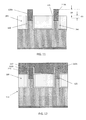
FIG. 13 is an exemplary perspective view corresponding to FIG. 12, illustrating one of Fin FETs of FIG. 12.
After the gate structure is formed, source and drain 240 are formed. The source and drain 240 may be formed by forming silicide layers on the upper portions of the fin structure not covered by the gate structure in some embodiments. In other embodiments, the upper portions of the fin structure not covered by the gate structure is recessed below the upper surface of the isolation insulating layer 180, and a strain material is re-grown over the recessed fin structure. The strain material may include one or more layers of Si, SiC, SiCP, SiP, SiCP, SiGe or Ge.
FIGS. 14A and 14B are exemplary cross sectional views of source/drain structures. In the present embodiment, the remaining second semiconductor layer 125 (made of e.g., Si) is disposed between the first semiconductor layer 110 and the channel region 210A in the p-type Fin FET. With this structure, even when depletion region 245 below the source/drain 240 expands, there is no current leakage path from the source/drain to the first semiconductor layer 110 and/or between the source and drain, as shown in FIG. 14A. In contrast, if there is no such remaining second semiconductor layer 125 (made of e.g., Si) between the first semiconductor layer 110 and the channel region 210A, there would be current leakage path from the source/drain to the first semiconductor layer 110 and/or between the source and drain, as shown in FIG. 14B.
Further, by interposing the remaining second semiconductor layer 125 (made of e.g., Si) is disposed between the first semiconductor layer 110 (made of e.g., for example Si(1-x)Gex, where x is in a range of about 0.1 to about 0.5) and the channel region 210A (made of, for example, for example Ge or a Si(1-z)Gez, where z is larger than x of the first semiconductor layer 110 (Si(1-x)Gex)), it is possible to suppress Ge diffusion between the first semiconductor layer 110 and the channel region 210A. In addition, by reducing annealing temperature for the isolation insulating layer 180, the Ge diffusion can be further suppressed.
In some embodiments, during thermal operations after forming the third semiconductor layer 210, Ge in the first and/or third semiconductor layers may diffuse into the remaining second semiconductor layer 125. Accordingly, the remaining second semiconductor layer 125 may contain Ge in an amount of about 10 atm % or less. In other embodiments, the Ge amount in the remaining second semiconductor layer 125 may be less than about 5 atm %.
It is understood that the Fin FET device may undergo further CMOS processes to form various features such as contacts/vias, interconnect metal layers, dielectric layers, passivation layers, etc.
FIGS. 15 and 16 are cross sectional views illustrating a sequential process for manufacturing a semiconductor FET device according to a modified embodiment of the present disclosure.
In FIG. 9 of the above embodiment, the second semiconductor layer 120 for the p-type Fin FET is partially etched and the bottom part of the second semiconductor layer 120 remains in the opening 190. The etching of the second semiconductor layer 120 may be performed by dry etching and/or wet etching.
In the modified embodiment, as shown in FIG. 15, the second semiconductor layer 120 for the p-type Fin FET is substantially fully etched so as to expose the upper surface of the first semiconductor layer 110A. Then, as shown in FIG. 16, a fourth semiconductor layer 125′ is formed over the exposed upper surface of the first semiconductor layer 110A in the opening 190, with a desired thickness D2. The fourth semiconductor layer 125′ is made of, for example, Si or Si(1-y)Gey, where y is less than about 0.1. In this modified embodiment, the material for the fourth semiconductor layer can be independently selected from the material for the channel region 120A (the second semiconductor layer) in the n-type Fin FET. Further, the thickness D2 can be more precisely controlled by using a relatively slow epitaxial growth for the fourth semiconductor layer 125′, compared with partially etching the second semiconductor layer. Moreover, it is possible to form the third semiconductor layer 210 continuously over the fourth semiconductor layer 125′ by changing a source gas(es).
FIGS. 17-24 are exemplary cross sectional views illustrating a sequential process for manufacturing a semiconductor FET device according to another embodiment of the present disclosure. It is understood that additional operations can be provided before, during, and after the operations shown by FIGS. 17-24, and some of the operations described below can be replaced or eliminated for additional embodiments of the method. The order of the operations may be interchangeable. Further, some of the features, materials, structures, processes and/or operations of this embodiment are substantially the same as or similar to those in the aforementioned embodiments with respect to FIGS. 1-16, and the detailed explanation thereof may be omitted.
As shown in FIG. 17, a first semiconductor layer 110 is epitaxially grown over the surface of the substrate 100. Further, a mask layer including a first layer 130 and a second layer 140 is formed over the second semiconductor layer 120.
The first semiconductor layer 110 is, for example Si(1-x)Gex, where x is in a range of about 0.1 to about 0.5. In some embodiments, x in Si(1-x)Gex may be in a range of about 0.2 to about 0.4. The thickness of the SiGe first semiconductor layer 110 is in a range of about 0.5 μm to about 2 μm in some embodiments. By growing a relatively thick SiGe layer 110 over the Si substrate 100, the stress induced in the SiGe layer 110 can be reduced and relaxed. In some embodiments, the thickness of the SiGe first semiconductor layer 110 is in a range of about 1 μm to about 1.5 μm. In certain embodiments, a Ge layer or a Si(1-x)Gex, where x is less than about 0.1, may be used as the first semiconductor layer 110. In other embodiments, III-V compound semiconductors such as GaAs, GaP, GaN, InP, InAs, InSb, GaAsP, AlGaN, AlInAs, AlGaAs, GaInAs, GaInP, and/or GaInAsP may be used as the first semiconductor layer 110.
The first semiconductor layer 110 may be doped or may not be doped. The doping may be performed during the epitaxial growth of the first semiconductor layer 110 or may be performed by ion implantation.
The mask layer may include, for example, a pad oxide (e.g., silicon oxide) layer 130 and a silicon nitride (SiN) mask layer 140 in some embodiments. The thickness of the pad oxide layer is in a range of about 2 nm to about 15 nm and the thickness of the silicon nitride mask layer is in a range of about 10 nm to about 50 nm in some embodiments.
As shown in FIG. 18, the first semiconductor layer 110 is patterned into fin structures. Similar to FIG. 2, by using the mask pattern 150 as etching masks, the first semiconductor layer 110 is pattered into fin structures 110B (10′ and 20′) by trench etching using a dry etching method and/or a wet etching method. As shown in FIG. 18, the trench etching is performed through to the middle of the first semiconductor layer 110. The fin structure 10′ is for a p-type Fin FET and the fin structure 20′ is for an n-type Fin FET.
The width of the fin structures 110B is in a range of about 5 nm to about 40 nm in some embodiments, and may be in a range of about 7 nm to about 15 nm in certain embodiments. The height H1 of the fin structures 110B is in a range of about 50 nm to about 300 nm in some embodiments, and may be in a range of about 100 nm to 200 nm in other embodiments. The space between adjacent fin structures is in a range of about 5 nm to about 80 nm in some embodiments, and may be in a range of about 7 nm to 15 nm in other embodiments. The remaining thickness H2 of the first semiconductor layer 110 is in a range of about 500 μm to about 800 μm.
After forming the fin structures, similar to FIG. 3, a protective layer 160 is formed to cover the fin structures 110B, as shown in FIG. 19. The protective layer 160 is made of a material that prevents the first semiconductor layer from being oxidized. In some embodiments, the protective layer 160 is made of one or more layers of silicon nitride (SiN), SiC, SiOCN and SiCN. The thickness of the protective layer 160 is in a range of about 1 nm to about 10 nm in some embodiments. In certain embodiments, the thickness of the protective layers 160 is in a range of about 2 nm to about 5 nm in some embodiments. In this embodiment, SiN is used as the protective layers 160. The protective layer 160 is formed by chemical vapor deposition CVD, plasma-enhanced chemical vapor deposition (PECVD), atmospheric pressure chemical vapor deposition (APCVD), a low-pressure CVD (LPCVD), high density plasma CVD (HDPCVD) and/or atomic layer deposition (ALD), and/or other suitable processes.
During the film formation process, the substrate temperature is in a range of 300° C. to 500° C. In some embodiments, the substrate temperature may be in a range of 350° C. to 450° C. By maintaining the substrate temperature relatively lower than a typical CVD process during the film formation process, it is possible to suppress diffusion of germanium in the first semiconductor layer into the second semiconductor layer. In some embodiments, PECVD is utilized.
After the protective layer 160 is formed, similar to FIG. 4, a sacrificial layer 170 is formed so that the fin structures 110B are embedded in the sacrificial layer 170. The fin structures 110B may be fully or partially embedded in the sacrificial layer 170. In some embodiments, the sacrificial layer 170 is made of an organic material such as a photo resist layer or a material for a bottom antireflective coating (BARC).
Then, similar to FIG. 5, the thickness of the sacrificial layer 170 is reduced by, for example, an etch-back process so as to expose a part of the fin structures, as shown in FIG. 20. The etch-back process may be performed by using plasma including O2 and at least one of CF4 and CHF3, at a temperature in a range about 0° C. to about 300° C. and at a pressure in a range of about 1 to about 10 Torr in certain embodiments. By adjusting etching time, a desired thickness of the remaining sacrificial layer can be obtained. In the present disclosure, the thickness H3 is in a range of about 20 nm to about 80 nm in some embodiments, and may be in a range of about 30 nm to about 60 nm in other embodiments.
Instead of etching-back the thick sacrificial layer, it may be possible to form a thin sacrificial layer having the target thickness directly by adjusting, for example, film forming condition.
Next, similar to FIG. 6, the upper portions of the protective layer 160 exposed from the sacrificial layer 170 are removed by, for example, dry etching and/or wet etching, as shown in FIG. 21.
Then, similar to FIG. 7, isolation insulating layer 180 is formed. The isolation insulating layer 180 is made of one or more layers of, for example, silicon dioxide, SiO, SiON, SiOCN or fluorine-doped silicate glass (FSG), or any other suitable dielectric material. When the isolation insulating layer 180 is made of silicon oxide, the silicon oxide may be doped with, for example, boron and/or phosphorous. In some embodiments of the present disclosure, the isolation insulating layer 180 may be formed by a flowable CVD (FCVD).
After the flowable film is deposited, it is cured and then annealed to remove undesired element(s) to form silicon oxide. When the undesired element(s) is removed, the flowable film densifies and shrinks. In some embodiments, multiple anneal processes are conducted. The flowable film is cured and annealed more than once. In the present embodiment, the temperatures for annealing are also adjusted to relatively lower temperatures, such as in a range from about 500° C. to about 800° C. Since the side walls of the bottom portion of the fin structures 110B are covered by the protective layer 160, the bottom portion of the fin structures 110B are not oxidized during the thermal process for forming the isolation insulating layer 180.
Similar to FIG. 8, the upper portions of the isolation insulating layers 180 and the mask patterns 150 are removed by, for example, a chemical mechanical polishing (CMP) method or other planarization methods such as an etch-back process, as shown in FIG. 22.
Then, as shown in FIG. 23, the upper portions of the fin structures 110B are partially recessed, thereby forming openings 190′. The etching of the upper portions of the fin structures 110B may be performed by dry etching and/or wet etching. In this embodiment, the upper portions of the fin structures 110B is etched to the depth D1 measured from the upper end of the protective layers 160. In some embodiments, the distance D1 is in a range of about 10 nm to about 60 nm, or may be in a range of about 20 nm to 50 nm in other embodiments.
After forming the openings 190′, the fifth semiconductor layers 120′ are epitaxially formed in the openings 190′, as shown in FIG. 24. The fifth semiconductor layer 120′ is, for example, Si or Si(1-y)Gey, where y is less than about 0.1. In this embodiment, the second semiconductor layer is Si. The fifth semiconductor layer 120′ has a thickness in a range of about 30 nm to about 200 nm in some embodiments. In certain embodiments, the thickness of the fifth semiconductor layer 120′ is in a range of about 50 nm to about 150 nm. The resultant structure shown in FIG. 24 is substantially the same as that shown in FIG. 8.
After the structure of FIG. 24 is formed, the similar operations of FIG. 9-12 or 15-16 are performed to obtain the structures of FIGS. 12 and 13. It is understood that the Fin FET device may undergo further CMOS processes to form various features such as contacts/vias, interconnect metal layers, dielectric layers, passivation layers, etc.
The various embodiments or examples described herein offer several advantages over the existing art. In some embodiments of the present disclosure, by interposing the remaining second semiconductor layer (made of e.g., Si) is disposed between the first semiconductor layer (made of e.g., for example Si(1-x)Gex, where x is in a range of about 0.1 to about 0.5) and the channel region (made of, for example, for example Ge or a Si(1-z)Gez, where z is larger than x of the first semiconductor layer (Si(1-x)Gex)) in a p-type FET, it is possible to suppress Ge diffusion between the first semiconductor layer and the channel region. In addition, by reducing annealing temperature for the isolation insulating layer, the Ge diffusion can be further suppressed. Moreover, it is possible to suppress leakages at the source drain regions.
It will be understood that not all advantages have been necessarily discussed herein, no particular advantage is required for all embodiments or examples, and other embodiments or examples may offer different advantages.
In accordance with one aspect of the present disclosure, in a method for manufacturing a semiconductor device, a first semiconductor layer is formed on a substrate. A second semiconductor layer is formed on the first semiconductor layer. A fin structure is formed by patterning the first and second semiconductor layers. The fin structure includes a bottom portion constituted of the first semiconductor layer and an upper portion constituted of the second semiconductor layer. A cover layer is formed on a bottom part of the fin structure so as to cover side walls of the bottom portion of the fin structure and a bottom part of side walls of the upper portion of the fin structure. An insulating layer is formed over the fin structure with the cover layer so that the fin structure is embedded in the insulating layer. A part of the upper portion of the fin structure is removed so that an opening is formed in the insulating layer and a layer of the second semiconductor layer remains in bottom of the opening. A third semiconductor layer is formed in the opening on the remaining layer of the second semiconductor layer. The insulating layer is recessed so that at least a part of the third semiconductor layer is exposed from the insulating layer. A gate structure is formed over the exposed third semiconductor layer.
In accordance with another aspect of the present disclosure, in a method for manufacturing a semiconductor device, a first semiconductor layer is formed on a substrate. A second semiconductor layer is formed on the first semiconductor layer. A first fin structure and a second fin structure are formed by patterning the first and second semiconductor layers. The first and second fin structures respectively include a bottom portion constituted of the first semiconductor layer and an upper portion constituted of the second semiconductor layer. A cover layer is formed on bottom parts of the first and second fin structures so as to cover side walls of the bottom portions of the first and second fin structures and bottom parts of side walls of the upper portion of the first and second fin structures. An insulating layer is formed over the first and second fin structures with the cover layer so that the first and second fin structures are embedded in the insulating layer. A part of the upper portion of the first fin structure is removed so that an opening is formed in the insulating layer and a layer of the second semiconductor layer remains in bottom of the opening, while protecting the upper portion of the second fin structure so as not to be etched. A third semiconductor layer is formed in the opening on the remaining layer of the second semiconductor layer. The insulating layer is recessed so that at least a part of the third semiconductor layer and a part of the upper portion of the second fin structure are exposed from the insulating layer. A first gate structure is formed over the exposed third semiconductor layer and a second gate structure is formed over the exposed portion of the second fin structure.
In accordance with another aspect of the present disclosure, a semiconductor device includes a first Fin FET device. The first Fin FET device includes a first fin structure extending in a first direction and protruding from an isolation insulating layer. The first fin structure and the isolation insulating layer are disposed over a substrate. The first fin structure includes a first layer made of a first semiconductor material, a second layer made of a second semiconductor material disposed over the first layer and a third layer made of a third semiconductor material disposed over the second layer. The first Fin FET further includes a first cover layer disposed on a bottom part of the first fin structure so as to cover side walls of the bottom portion of the first fin structure and a bottom part of side walls of the upper portion of the first fin structure. The first Fin FET further includes a first gate stack including a gate electrode layer and a gate dielectric layer, covering a portion of the first fin structure and extending in a second direction perpendicular to the first direction. The third layer functions as a channel region of the first Fin FET. The first semiconductor material includes Si(1-x)Gex, the second semiconductor material includes Si(1-y)Gey, and the third semiconductor material includes Ge or a Si(1-z)Gez, where y is smaller than x, and z is larger than y.
The foregoing outlines features of several embodiments or examples so that those skilled in the art may better understand the aspects of the present disclosure. Those skilled in the art should appreciate that they may readily use the present disclosure as a basis for designing or modifying other processes and structures for carrying out the same purposes and/or achieving the same advantages of the embodiments or examples introduced herein. Those skilled in the art should also realize that such equivalent constructions do not depart from the spirit and scope of the present disclosure, and that they may make various changes, substitutions, and alterations herein without departing from the spirit and scope of the present disclosure.

Claims (20)

What is claimed is:
1. A method for manufacturing a semiconductor device, comprising:
forming a first semiconductor layer on a substrate;
forming a second semiconductor layer on the first semiconductor layer;
forming a fin structure by patterning the first and second semiconductor layers, the fin structure including a bottom portion constituted of the first semiconductor layer and an upper portion constituted of the second semiconductor layer;
forming a cover layer on a bottom part of the fin structure so as to cover side walls of the bottom portion of the fin structure and a bottom part of side walls of the upper portion of the fin structure;
forming an insulating layer over the fin structure with the cover layer so that the fin structure is embedded in the insulating layer;
removing a part of the upper portion of the fin structure so that an opening is formed in the insulating layer and a layer of the second semiconductor layer remains in a bottom portion of the opening;
forming a third semiconductor layer in the opening on the remaining layer of the second semiconductor layer;
recessing the insulating layer so that at least a part of the third semiconductor layer is exposed from the insulating layer; and
forming a gate structure over the exposed third semiconductor layer.
2. The method of claim 1, wherein:
the first semiconductor layer includes Si(1-x)Gex,
the second semiconductor layer includes Si(1-y)Gey,
the third semiconductor layer includes Ge or a Si(1-z)Gez, and
y is smaller than x, and
z is larger than y.
3. The method of claim 2, wherein x is in a range of 0.1 to 0.5.
4. The method of claim 2, wherein y is equal to zero or less than 0.1.
5. The method of claim 4, wherein:
in the forming a second semiconductor layer on the first semiconductor layer, Si is formed as the second semiconductor layer, and
after the forming a gate structure, the remaining layer of the second semiconductor layer contains Ge in an amount of less than 10 atm %.
6. The method of claim 2, wherein z is equal to or more than 0.5.
7. The method of claim 1, wherein the forming a cover layer includes:
forming a blanket layer of a cover layer material over the fin structure;
forming a sacrificial layer to cover a bottom portion of the fin structure with the blanket layer so that an upper portion of the fin structure with the blanket layer is exposed from the sacrificial layer; and
removing the blanket layer on the upper portion of the fin structure exposed from the sacrificial layer.
8. The method of claim 1, wherein an upper end of the cover layer is 10 nm to 60 nm higher than an interface between the first semiconductor layer and the second semiconductor layer.
9. The method of claim 1, wherein the cover layer includes silicon nitride.
10. The method of claim 1, wherein the insulating layer is formed by CVD followed by annealing at a temperature less than 800° C.
11. A method for manufacturing a semiconductor device, comprising:
forming a first semiconductor layer on a substrate;
forming a second semiconductor layer on the first semiconductor layer;
forming a first fin structure and a second fin structure by patterning the first and second semiconductor layers, the first and second fin structures respectively including a bottom portion constituted of the first semiconductor layer and an upper portion constituted of the second semiconductor layer;
forming a cover layer on bottom parts of the first and second fin structures so as to cover side walls of the bottom portions of the first and second fin structures and bottom parts of side walls of the upper portion of the first and second fin structures;
forming an insulating layer over the first and second fin structures with the cover layer so that the first and second fin structures are embedded in the insulating layer;
removing a part of the upper portion of the first fin structure so that an opening is formed in the insulating layer and a layer of the second semiconductor layer remains in a bottom portion of the opening, while protecting the upper portion of the second fin structure so as not to be etched;
forming a third semiconductor layer in the opening on the remaining layer of the second semiconductor layer;
recessing the insulating layer so that at least a part of the third semiconductor layer and a part of the upper portion of the second fin structure are exposed from the insulating layer; and
forming a first gate structure over the exposed third semiconductor layer and a second gate structure over the exposed portion of the second fin structure.
12. The method of claim 11, wherein:
the first semiconductor layer includes Si(1-x)Gex,
the second semiconductor layer includes Si(1-y)Gey,
the third semiconductor layer includes Ge or a Si(1-z)Gez, and
y is smaller than x, and
z is larger than y.
13. The method of claim 12, wherein:
x is in a range of 0.1 to 0.5, and
y is equal to zero or less than 0.1.
14. The method of claim 13, wherein:
in the forming a second semiconductor layer on the first semiconductor layer, Si is formed as the second semiconductor layer, and
after the forming a gate structure, the remaining layer of the second semiconductor layer contains Ge in an amount of less than 10 atm %.
15. The method of claim 11, wherein the forming a cover layer includes:
forming a blanket layer of a cover layer material over the first and second fin structures;
forming a sacrificial layer to cover bottom portions of the first and second fin structures with the blanket layer so that upper portions of the first and second fin structures with the blanket layer expose from the sacrificial layer; and
removing the blanket layer on the upper portions of the first and second fin structures are exposed from the sacrificial layer.
16. The method of claim 11, wherein an upper end of the cover layer is 10 nm to 60 nm higher than an interface between the first semiconductor layer and the second semiconductor layer.
17. The method of claim 11, wherein the cover layer includes silicon nitride.
18. The method of claim 11, wherein the insulating layer is formed by CVD followed by annealing at a temperature less than 800° C.
19. A semiconductor device comprising a first fin field effect transistor (Fin FET), the first Fin FET including:
a first fin structure extending in a first direction and protruding from an isolation insulating layer, the first fin structure and the isolation insulating layer being disposed over a substrate, the first fin structure including a first layer made of a first semiconductor material, a second layer made of a second semiconductor material disposed over the first layer and a third layer made of a third semiconductor material disposed over the second layer;
a first cover layer disposed on a bottom part of the first fin structure so as to cover side walls of a bottom portion of the first fin structure and a bottom part of side walls of the upper portion of the first fin structure;
a first gate stack including a gate electrode layer and a gate dielectric layer, covering a portion of the first fin structure and extending in a second direction perpendicular to the first direction, wherein:
the third layer functions as a channel region of the first Fin FET,
the first semiconductor material includes Si(1-x)Gex,
the second semiconductor material includes Si(1-y)Gey,
the third semiconductor material includes Ge or a Si(1-z)Gez, and
y is smaller than x, and
z is larger than y.
20. The semiconductor device of claim 19, further comprising a second Fin FET, the second Fin FET including:
a second fin structure extending in the first direction and protruding from the isolation insulating layer, the second fin structure being disposed over the substrate, the second fin structure including a first layer made of the first semiconductor material and a second layer made of the second semiconductor material disposed over the first layer;
a second cover layer disposed on a bottom part of the second fin structure so as to cover side walls of a bottom portion of the second fin structure and a bottom part of side walls of the upper portion of the second fin structure;
a second gate stack including a gate electrode layer and a gate dielectric layer, covering a portion of the second fin structure and extending in the second direction perpendicular to the second direction,
wherein the second layer functions as a channel region of the second Fin FET.
US14/927,190 2015-10-29 2015-10-29 Semiconductor device and manufacturing method thereof Expired - Fee Related US9449882B1 (en)

Priority Applications (7)

Application Number Priority Date Filing Date Title
US14/927,190 US9449882B1 (en) 2015-10-29 2015-10-29 Semiconductor device and manufacturing method thereof
TW105124581A TWI611459B (en) 2015-10-29 2016-08-03 Semiconductor device and method of manufacturing same
US15/242,155 US10163728B2 (en) 2015-10-29 2016-08-19 Semiconductor device having a stacked fin structure and manufacturing method thereof
DE102016117473.4A DE102016117473A1 (en) 2015-10-29 2016-09-16 SEMICONDUCTOR DEVICE AND METHOD FOR MANUFACTURING THEM
CN201610907124.7A CN106992154B (en) 2015-10-29 2016-10-19 Semiconductor device and method of manufacturing the same
KR1020160135693A KR20170051269A (en) 2015-10-29 2016-10-19 Semiconductor device and manufacturing method thereof
KR1020180127512A KR101946765B1 (en) 2015-10-29 2018-10-24 Semiconductor device and manufacturing method thereof

Applications Claiming Priority (1)

Application Number Priority Date Filing Date Title
US14/927,190 US9449882B1 (en) 2015-10-29 2015-10-29 Semiconductor device and manufacturing method thereof

Related Child Applications (1)

Application Number Title Priority Date Filing Date
US15/242,155 Continuation US10163728B2 (en) 2015-10-29 2016-08-19 Semiconductor device having a stacked fin structure and manufacturing method thereof

Publications (1)

Publication Number Publication Date
US9449882B1 true US9449882B1 (en) 2016-09-20

Family

ID=56896175

Family Applications (2)

Application Number Title Priority Date Filing Date
US14/927,190 Expired - Fee Related US9449882B1 (en) 2015-10-29 2015-10-29 Semiconductor device and manufacturing method thereof
US15/242,155 Active US10163728B2 (en) 2015-10-29 2016-08-19 Semiconductor device having a stacked fin structure and manufacturing method thereof

Family Applications After (1)

Application Number Title Priority Date Filing Date
US15/242,155 Active US10163728B2 (en) 2015-10-29 2016-08-19 Semiconductor device having a stacked fin structure and manufacturing method thereof

Country Status (5)

Country Link
US (2) US9449882B1 (en)
KR (2) KR20170051269A (en)
CN (1) CN106992154B (en)
DE (1) DE102016117473A1 (en)
TW (1) TWI611459B (en)

Cited By (3)

* Cited by examiner, † Cited by third party
Publication number Priority date Publication date Assignee Title
US20180068866A1 (en) * 2016-09-05 2018-03-08 Semiconductor Manufacturing International (Shanghai) Corporation Semiconductor device and fabrication method thereof
CN109087861A (en) * 2017-06-14 2018-12-25 中芯国际集成电路制造(上海)有限公司 Semiconductor devices and forming method thereof
US10163728B2 (en) * 2015-10-29 2018-12-25 Taiwan Semiconductor Manufacturing Co., Ltd. Semiconductor device having a stacked fin structure and manufacturing method thereof

Families Citing this family (6)

* Cited by examiner, † Cited by third party
Publication number Priority date Publication date Assignee Title
US9960273B2 (en) * 2015-11-16 2018-05-01 Taiwan Semiconductor Manufacturing Company, Ltd. Integrated circuit structure with substrate isolation and un-doped channel
US10043900B1 (en) 2017-03-20 2018-08-07 International Business Machines Corporation Vertical transport Fin field effect transistors on a substrate with varying effective gate lengths
CN110034068B (en) * 2018-01-11 2021-07-13 中芯国际集成电路制造(上海)有限公司 Semiconductor structure and method of forming the same
US11424165B2 (en) 2019-10-16 2022-08-23 Taiwan Semiconductor Manufacturing Co., Ltd. Method of manufacturing semiconductor devices having different gate dielectric thickness within one transistor
KR102868050B1 (en) * 2020-09-04 2025-10-01 삼성전자주식회사 Field effect transistor and method of manufacturing the same
CN115020238B (en) * 2022-06-20 2026-02-17 上海积塔半导体有限公司 Semiconductor structure and preparation method thereof

Citations (4)

* Cited by examiner, † Cited by third party
Publication number Priority date Publication date Assignee Title
US20120104472A1 (en) * 2010-10-18 2012-05-03 Taiwan Semiconductor Manufacturing Company, Ltd. Fin-like field effect transistor (finfet) device and method of manufacturing same
US20120319211A1 (en) * 2011-06-16 2012-12-20 Taiwan Semiconductor Manufacturing Company, Ltd. Strained channel field effect transistor
US8367498B2 (en) * 2010-10-18 2013-02-05 Taiwan Semiconductor Manufacturing Company, Ltd. Fin-like field effect transistor (FinFET) device and method of manufacturing same
US20150311341A1 (en) * 2014-04-25 2015-10-29 Sung Gi Hur Semiconductor device having fin-type field effect transistor and method of manufacturing the same

Family Cites Families (11)

* Cited by examiner, † Cited by third party
Publication number Priority date Publication date Assignee Title
JP2005064500A (en) * 2003-08-14 2005-03-10 Samsung Electronics Co Ltd Multi-structure silicon fin and manufacturing method
KR100496891B1 (en) 2003-08-14 2005-06-23 삼성전자주식회사 Silicon fin for finfet and method for fabricating the same
KR100578130B1 (en) * 2003-10-14 2006-05-10 삼성전자주식회사 Multiple Silicon Fins and Their Formation Methods for Fin Field Effect Transistors
US7834403B2 (en) * 2007-08-13 2010-11-16 Infineon Technologies Ag Bipolar transistor FINFET technology
US8618556B2 (en) 2011-06-30 2013-12-31 Taiwan Semiconductor Manufacturing Company, Ltd. FinFET design and method of fabricating same
EP2701198A3 (en) * 2012-08-24 2017-06-28 Imec Device with strained layer for quantum well confinement and method for manufacturing thereof
US8766363B2 (en) * 2012-11-07 2014-07-01 International Business Machines Corporation Method and structure for forming a localized SOI finFET
US8866204B2 (en) * 2013-01-30 2014-10-21 Stmicroelectronics, Inc. Method to form finFET/trigate devices on bulk semiconductor wafers
US9153647B1 (en) * 2014-03-17 2015-10-06 International Business Machines Corporation Integrated circuit having heterostructure FinFET with tunable device parameters and method to fabricate same
US9589849B2 (en) * 2015-02-27 2017-03-07 Globalfoundries Inc. Methods of modulating strain in PFET and NFET FinFET semiconductor devices
US9449882B1 (en) * 2015-10-29 2016-09-20 Taiwan Semiconductor Manufacturing Co., Ltd. Semiconductor device and manufacturing method thereof

Patent Citations (4)

* Cited by examiner, † Cited by third party
Publication number Priority date Publication date Assignee Title
US20120104472A1 (en) * 2010-10-18 2012-05-03 Taiwan Semiconductor Manufacturing Company, Ltd. Fin-like field effect transistor (finfet) device and method of manufacturing same
US8367498B2 (en) * 2010-10-18 2013-02-05 Taiwan Semiconductor Manufacturing Company, Ltd. Fin-like field effect transistor (FinFET) device and method of manufacturing same
US20120319211A1 (en) * 2011-06-16 2012-12-20 Taiwan Semiconductor Manufacturing Company, Ltd. Strained channel field effect transistor
US20150311341A1 (en) * 2014-04-25 2015-10-29 Sung Gi Hur Semiconductor device having fin-type field effect transistor and method of manufacturing the same

Cited By (5)

* Cited by examiner, † Cited by third party
Publication number Priority date Publication date Assignee Title
US10163728B2 (en) * 2015-10-29 2018-12-25 Taiwan Semiconductor Manufacturing Co., Ltd. Semiconductor device having a stacked fin structure and manufacturing method thereof
US20180068866A1 (en) * 2016-09-05 2018-03-08 Semiconductor Manufacturing International (Shanghai) Corporation Semiconductor device and fabrication method thereof
US10586713B2 (en) * 2016-09-05 2020-03-10 Semiconductor Manufacturing International (Shanghai) Corporation Semiconductor device and fabrication method thereof
CN109087861A (en) * 2017-06-14 2018-12-25 中芯国际集成电路制造(上海)有限公司 Semiconductor devices and forming method thereof
CN109087861B (en) * 2017-06-14 2022-02-15 中芯国际集成电路制造(上海)有限公司 Semiconductor device and method of forming the same

Also Published As

Publication number Publication date
KR20170051269A (en) 2017-05-11
US10163728B2 (en) 2018-12-25
CN106992154A (en) 2017-07-28
DE102016117473A1 (en) 2017-05-04
CN106992154B (en) 2020-05-15
KR101946765B1 (en) 2019-02-11
KR20180118586A (en) 2018-10-31
TWI611459B (en) 2018-01-11
TW201730918A (en) 2017-09-01
US20170125304A1 (en) 2017-05-04

Similar Documents

Publication Publication Date Title
US10644154B2 (en) Semiconductor device and manufacturing method thereof
US11705519B2 (en) Semiconductor device and manufacturing method thereof
US10347751B2 (en) Self-aligned epitaxy layer
US10269935B2 (en) Semiconductor device including Fin-PET and manufacturing method thereof
US10163728B2 (en) Semiconductor device having a stacked fin structure and manufacturing method thereof
US10068992B2 (en) Semiconductor device including fin FET and manufacturing method thereof
US10276574B2 (en) Semiconductor device and manufacturing method thereof
US9818846B2 (en) Selectively deposited spacer film for metal gate sidewall protection
US9530889B2 (en) Semiconductor device and manufacturing method thereof
US9691903B2 (en) Semiconductor device and manufacturing method thereof
US11404418B2 (en) Semiconductor device and manufacturing method thereof

Legal Events

Date Code Title Description
AS Assignment

Owner name: TAIWAN SEMICONDUCTOR MANUFACTURING CO., LTD., TAIW

Free format text: ASSIGNMENT OF ASSIGNORS INTEREST;ASSIGNORS:WANG, SHENG-CHEN;LEE, KAI-HSUAN;YEONG, SAI-HOOI;AND OTHERS;REEL/FRAME:038413/0889

Effective date: 20151221

STCF Information on status: patent grant

Free format text: PATENTED CASE

MAFP Maintenance fee payment

Free format text: PAYMENT OF MAINTENANCE FEE, 4TH YEAR, LARGE ENTITY (ORIGINAL EVENT CODE: M1551); ENTITY STATUS OF PATENT OWNER: LARGE ENTITY

Year of fee payment: 4

FEPP Fee payment procedure

Free format text: MAINTENANCE FEE REMINDER MAILED (ORIGINAL EVENT CODE: REM.); ENTITY STATUS OF PATENT OWNER: LARGE ENTITY

LAPS Lapse for failure to pay maintenance fees

Free format text: PATENT EXPIRED FOR FAILURE TO PAY MAINTENANCE FEES (ORIGINAL EVENT CODE: EXP.); ENTITY STATUS OF PATENT OWNER: LARGE ENTITY

STCH Information on status: patent discontinuation

Free format text: PATENT EXPIRED DUE TO NONPAYMENT OF MAINTENANCE FEES UNDER 37 CFR 1.362

STCH Information on status: patent discontinuation

Free format text: PATENT EXPIRED DUE TO NONPAYMENT OF MAINTENANCE FEES UNDER 37 CFR 1.362

FP Lapsed due to failure to pay maintenance fee

Effective date: 20240920