US9449684B2 - Storage control device, storage device, information processing system, and storage control method - Google Patents
Storage control device, storage device, information processing system, and storage control method Download PDFInfo
- Publication number
- US9449684B2 US9449684B2 US14/454,214 US201414454214A US9449684B2 US 9449684 B2 US9449684 B2 US 9449684B2 US 201414454214 A US201414454214 A US 201414454214A US 9449684 B2 US9449684 B2 US 9449684B2
- Authority
- US
- United States
- Prior art keywords
- memory cell
- refreshing
- request
- data
- cell array
- Prior art date
- Legal status (The legal status is an assumption and is not a legal conclusion. Google has not performed a legal analysis and makes no representation as to the accuracy of the status listed.)
- Expired - Fee Related, expires
Links
Images


Classifications
-
- G—PHYSICS
- G11—INFORMATION STORAGE
- G11C—STATIC STORES
- G11C13/00—Digital stores characterised by the use of storage elements not covered by groups G11C11/00, G11C23/00, or G11C25/00
- G11C13/0002—Digital stores characterised by the use of storage elements not covered by groups G11C11/00, G11C23/00, or G11C25/00 using resistive RAM [RRAM] elements
- G11C13/0021—Auxiliary circuits
- G11C13/004—Reading or sensing circuits or methods
-
- G—PHYSICS
- G11—INFORMATION STORAGE
- G11C—STATIC STORES
- G11C13/00—Digital stores characterised by the use of storage elements not covered by groups G11C11/00, G11C23/00, or G11C25/00
- G11C13/0002—Digital stores characterised by the use of storage elements not covered by groups G11C11/00, G11C23/00, or G11C25/00 using resistive RAM [RRAM] elements
- G11C13/0007—Digital stores characterised by the use of storage elements not covered by groups G11C11/00, G11C23/00, or G11C25/00 using resistive RAM [RRAM] elements comprising metal oxide memory material, e.g. perovskites
-
- G—PHYSICS
- G11—INFORMATION STORAGE
- G11C—STATIC STORES
- G11C13/00—Digital stores characterised by the use of storage elements not covered by groups G11C11/00, G11C23/00, or G11C25/00
- G11C13/0002—Digital stores characterised by the use of storage elements not covered by groups G11C11/00, G11C23/00, or G11C25/00 using resistive RAM [RRAM] elements
- G11C13/0021—Auxiliary circuits
- G11C13/0033—Disturbance prevention or evaluation; Refreshing of disturbed memory data
-
- G—PHYSICS
- G11—INFORMATION STORAGE
- G11C—STATIC STORES
- G11C13/00—Digital stores characterised by the use of storage elements not covered by groups G11C11/00, G11C23/00, or G11C25/00
- G11C13/0002—Digital stores characterised by the use of storage elements not covered by groups G11C11/00, G11C23/00, or G11C25/00 using resistive RAM [RRAM] elements
- G11C13/0021—Auxiliary circuits
- G11C13/0035—Evaluating degradation, retention or wearout, e.g. by counting writing cycles
-
- G—PHYSICS
- G11—INFORMATION STORAGE
- G11C—STATIC STORES
- G11C13/00—Digital stores characterised by the use of storage elements not covered by groups G11C11/00, G11C23/00, or G11C25/00
- G11C13/0002—Digital stores characterised by the use of storage elements not covered by groups G11C11/00, G11C23/00, or G11C25/00 using resistive RAM [RRAM] elements
- G11C13/0021—Auxiliary circuits
- G11C13/0069—Writing or programming circuits or methods
-
- G—PHYSICS
- G11—INFORMATION STORAGE
- G11C—STATIC STORES
- G11C29/00—Checking stores for correct operation ; Subsequent repair; Testing stores during standby or offline operation
- G11C29/04—Detection or location of defective memory elements, e.g. cell constructio details, timing of test signals
- G11C29/08—Functional testing, e.g. testing during refresh, power-on self testing [POST] or distributed testing
- G11C29/12—Built-in arrangements for testing, e.g. built-in self testing [BIST] or interconnection details
- G11C29/38—Response verification devices
- G11C29/42—Response verification devices using error correcting codes [ECC] or parity check
-
- G—PHYSICS
- G11—INFORMATION STORAGE
- G11C—STATIC STORES
- G11C29/00—Checking stores for correct operation ; Subsequent repair; Testing stores during standby or offline operation
- G11C29/56—External testing equipment for static stores, e.g. automatic test equipment [ATE]; Interfaces therefor
-
- G—PHYSICS
- G11—INFORMATION STORAGE
- G11C—STATIC STORES
- G11C13/00—Digital stores characterised by the use of storage elements not covered by groups G11C11/00, G11C23/00, or G11C25/00
- G11C13/0002—Digital stores characterised by the use of storage elements not covered by groups G11C11/00, G11C23/00, or G11C25/00 using resistive RAM [RRAM] elements
- G11C13/0021—Auxiliary circuits
- G11C13/0069—Writing or programming circuits or methods
- G11C2013/0076—Write operation performed depending on read result
Definitions
- the present application relates to a storage control device.
- the present application specifically relates to a storage control device, a storage device, and an information processing system for a non-volatile memory, a processing method thereof, and a program for executing the method by a computer.
- a dynamic random access memory (DRAM) or the like is used as a work memory in an information processing system.
- the DRAM is normally a volatile memory, and loses stored content therein when supply of power is stopped.
- a non-volatile memory (NVM) has been used.
- the non-volatile memory is broadly divided into a flash memory corresponding to a data access using units of a large size, and a non-volatile random access memory (NVRAM) which can perform a rapid random access using small units.
- NVRAM non-volatile random access memory
- a NAND-type flash memory is used as a representative example of the flash memory.
- a resistance RAM (ReRAM), a phase-change RAM (PCRAM), a magnetoresistive RAM (MRAM), or the like is used as the non-volatile random access memory.
- non-volatile memory data is read out by applying a voltage with respect to a memory cell. As the data is read out, the memory cell receives stress caused by the voltage. By repeating the reading-out of the data, that is, repeatedly applying stress caused by the voltage with respect to the memory cell, written data may be destroyed and an erroneous value may be read out from the memory cell.
- a technology of performing correction of data using an error correction code and rewriting the corrected data to a non-volatile memory to prevent data destruction, when an error is detected from the read-out data has been proposed (for example, see Japanese Unexamined Patent Application Publication No. 06-1107931.
- data destruction is prevented by rewriting corrected data to a non-volatile memory, which is a so-called refreshing process.
- removal and writing are performed with respect to all memory cells belonging to at least the same physical page, including a memory cell in which an error is generated.
- Data removal and writing of a memory cell in which rewriting of data is not necessary may be a reason for the long time taken for a process.
- the data removal and writing of a memory cell in which rewriting of data is not necessary may be a reason for increased stress applied to the memory cell and a short life of the non-volatile memory.
- a storage control device or a method thereof including: a detection unit which detects a first timing for performing a first rewriting process of performing only a first operation from among the first operation and a second operation, in a memory cell array in which each bit transitions to a first storage state by the first operation and transitions to a second storage state by the second operation; and a request unit which makes a request for the first rewriting process with respect to the memory cell array, when the first timing is detected. Accordingly, when there is significant degradation of bits supposed to be in the first storage state, for example, by using the rewriting process of performing only the first operation, the rewriting process with respect to the memory cell array is simplified.
- the detection unit may detect the first timing when the number of bits obtained by reading out bits supposed to be in the first storage state as bits in second storage state is greater than a predetermined number of bits. Accordingly, the rewriting process is switched based on the number of errors of bits supposed to be in the degraded first storage state, for example. In this case, the detection unit may start detection of the first timing, when the number of errors detected in the memory cell array is greater than a predetermined number of errors.
- the detection unit may compare the number of bits in the second storage state when predetermined data is written to the memory cell array, and the number of bits in the second storage state when the predetermined written data is read out from the memory cell array, and detect the first timing when the number of bits in the second storage state when the data is read out is greater. Accordingly, the rewriting process is switched based on the number of bits in the second storage state before and after the writing. In this case, the detection unit may start the detection of the first timing, when a difference between the number of bits in the second storage state when the data is written and the number of bits in the second storage state when the data is read out is greater than a predetermined number.
- the storage control device may further include an information management unit which records the number of times of reading for each physical address regarding the memory cell array, and the detection unit may detect the first timing for the physical address in which the number of times of reading reaches a predetermined number of times. Accordingly, the rewriting process is switched based on the number of times of reading.
- the information management unit may further record the number of times the power of the memory cell has been turned on, after making a request for a rewriting process of performing both the first operation and the second operation with respect to the memory cell array, and the detection unit may make a request for the rewriting process of performing both the first operation and the second operation with respect to the memory cell array, when the number of times the power has been turned on reaches a predetermined number of times.
- the detection unit may perform the detection of the first timing during execution of a reading command for performing reading-out from the memory cell array. Accordingly, the rewriting process is performed each time of executing the reading command.
- the detection unit may spontaneously perform the detection of the first timing in a state where a command for accessing the memory cell array is not executed. Accordingly, the storage control device performs the rewriting process at a spontaneous timing.
- the detection unit may detect the first timing when a predetermined period has elapsed after a first rewriting process is performed in the memory cell array. Accordingly, the rewriting process is performed according to the time elapsed from the last time point when the rewriting process is performed.
- the detection unit may further detect a second timing for performing a second rewriting process of performing both the first operation and the second operation, and the request unit may make a request for the second rewriting process with respect to the memory cell array when the second timing is detected. Accordingly, the second rewriting process is performed when the first rewriting process is insufficient.
- a storage device including: a memory cell array in which each bit transitions to a first storage state by a first operation and transitions to a second storage state by a second operation; a detection unit which detects a first timing for performing a first rewriting process of performing only the first operation from among the first operation and the second operation in the memory cell array; and a request unit which makes a request for the first rewriting process with respect to the memory cell array, when the first timing is detected. Accordingly, when there is significant degradation of bits supposed to be in the first storage state, for example, by using the rewriting process of performing only the first operation, the rewriting process with respect to the memory cell array is simplified.
- each bit of the memory cell array may be formed of a variable resistance element
- the first storage state may be a low resistance state
- the second storage state may be a high resistance state
- the first operation may be a setting operation for transitioning the bit to the low resistance state
- the second operation may be a resetting operation for transitioning the bit to the high resistance state.
- an information processing system including: a memory cell array in which each bit transitions to a first storage state by a first operation and transitions to a second storage state by a second operation; a host computer which issues a reading command with respect to the memory cell array; a detection unit which detects a first timing for performing a first rewriting process of performing only the first operation from among the first operation and the second operation regarding execution of the reading command; and a request unit which makes a request for the first rewriting process with respect to the memory cell array, when the first timing is detected.
- the rewriting process of the memory cell array is simplified by using the rewriting process of performing only the first operation.
- FIG. 1 is a diagram showing a configuration example of an information processing system according to an embodiment of the present application
- FIG. 2 is a diagram showing a configuration example of a memory according to an embodiment of the present application.
- FIG. 3 is a diagram showing an example of a structure of a memory cell array according to an embodiment of the present application.
- FIG. 4 is a diagram showing a circuit example of a memory cell according to an embodiment of the present application.
- FIG. 5 is a diagram showing a resistance distribution in a normal state of a memory cell according to an embodiment of the present application.
- FIG. 6 is a diagram showing a changed resistance distribution of a memory cell according to an embodiment of the present application.
- FIG. 7 is a diagram showing an example of a structure of data stored in a memory cell array according to an embodiment of the present application.
- FIG. 8 is a diagram showing an example of a structure of a physical page stored in a memory cell array according to an embodiment of the present application.
- FIG. 9 is a diagram showing an example of each buffer retained in a buffer according to an embodiment of the present application.
- FIG. 10 is a diagram showing a specific example retained in a buffer according to an embodiment of the present application.
- FIG. 11 is a diagram showing a specific example retained in a buffer according to an embodiment of the present application.
- FIG. 12 is a diagram showing a specific example retained in a buffer according to an embodiment of the present application.
- FIG. 13 is a diagram showing a specific example retained in a buffer according to an embodiment of the present application.
- FIG. 14 is a flowchart showing an example of a reading command process procedure of a memory controller according to a first embodiment of the present application
- FIG. 15 is a flowchart showing an example of a process procedure of a refreshing process (Step S 820 ) of a memory controller according to a first embodiment of the present application;
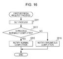
- FIG. 16 is a flowchart showing an example of a process procedure of a first refreshing request process of a memory according to an embodiment of the present application
- FIG. 17 is a flowchart showing an example of a process procedure of a second refreshing request process of a memory according to an embodiment of the present application.
- FIG. 18 is a flowchart showing an example of a process procedure of a setting process of a memory according to an embodiment of the present application.
- FIG. 19 is a flowchart showing an example of a process procedure of a resetting process of a memory according to an embodiment of the present application.
- FIG. 20 is a flowchart showing an example of a process procedure of a reading request process according to an embodiment of the present application.
- FIG. 21 is a flowchart showing an example of a reading command process procedure of a memory controller according to a second embodiment of the present application.
- FIG. 22 is a flowchart showing an example of a process procedure of a refreshing process of a memory controller according to a second embodiment of the present application.
- FIG. 23 is a diagram showing an example of a structure of a physical page stored in a memory cell array according to a third embodiment of the present application.
- FIG. 24 is a flowchart showing an example of a reading command process procedure of a memory controller according to a third embodiment of the present application.
- FIG. 25 is a flowchart showing an example of a process procedure of a refreshing process (Step S 850 ) of a memory controller according to a third embodiment of the present application;
- FIG. 26 is a diagram showing a configuration example of a refreshing information management table according to a fourth embodiment of the present application.
- FIG. 27 is a flowchart showing an example of a reading command process procedure of a memory controller according to a fourth embodiment of the present application.
- FIG. 28 is a flowchart showing an example of a process procedure of a refreshing process (Step S 860 ) of a memory controller according to a fourth embodiment of the present application;
- FIG. 29 is a flowchart showing an example of a refreshing execution confirmation process procedure of a memory controller according to a fourth embodiment of the present application.
- FIG. 30 is a flowchart showing an example of a process procedure of a refreshing process (Step S 880 ) of a memory controller according to a fourth embodiment of the present application;
- FIG. 31 is a diagram showing a configuration example of a refreshing information management table according to a fifth embodiment of the present application.
- FIG. 32 is a flowchart showing an example of a refreshing execution confirmation process procedure of a memory controller according to a fifth embodiment of the present application.
- FIG. 33 is a flowchart showing an example of a process procedure of a first refreshing process (Step S 720 ) of a memory controller according to a fifth embodiment of the present application;
- FIG. 34 is a flowchart showing an example of a process procedure of a second refreshing process (Step S 730 ) of a memory controller according to a fifth embodiment of the present application;
- FIG. 35 is a flowchart showing a modification example of a refreshing execution confirmation process procedure of a memory controller according to a fifth embodiment of the present application.
- FIG. 36 is a flowchart showing an example of a process procedure of a third refreshing process (Step S 740 ) of a memory controller according to a fifth embodiment of the present application;
- FIG. 37 is a flowchart showing an example of a process procedure of a third refreshing request process of a memory according to a fifth embodiment of the present application.
- FIG. 38 is a diagram showing a relationship between a resistance distribution of a memory cell and threshold values of a modification example according to a fifth embodiment of the present application.
- FIG. 39 is a diagram showing a resistance distribution chart for storing four states of a modification example according to an embodiment of the present application.
- embodiments for realizing the present application (hereinafter, referred to as embodiments) will be described.
- the embodiments will be described in the following order.
- FIG. 1 is a diagram showing a configuration example of an information processing system according to an embodiment of the present application.
- This information processing system is configured with a host computer 100 , a memory controller 200 , and a memory 300 .
- the memory controller 200 and the memory 300 configure a storage system.
- the host computer 100 issues a command for making a request for a reading process, a writing process, or a refreshing process of data with respect to the memory 300 .
- the memory controller 200 communicates with the host computer 100 and receives the command, and executes data writing to the memory 300 and data reading-out from the memory 300 .
- the memory controller 200 performs instruction of writing of data received from the host computer 100 to the memory 300 .
- the memory controller 200 reads out data from the memory 300 and transmits the data to the host computer 100 .
- the memory controller 200 performs instruction so as to read out data from the memory 300 and to rewrite the read-out data to the memory 300 .
- a logical address is used as an address showing location information of the data in the memory controller 200 . It is assumed that an area shown by one logical address has a size of 512 bytes. Meanwhile, when the memory controller 200 makes a request for writing or reading, a physical address is used as an address showing location information of data in the memory 300 . It is assumed that an area shown by one physical address has a size of 528 bytes (4224 bits).
- the memory controller 200 includes a processor 210 , a RAM 220 , a ROM 230 , an ECC processing unit 240 , a refreshing information management unit 250 , a host interface 201 , and a memory interface 203 .
- the processor 210 controls the entire memory controller 200 .
- the processor 210 executes software stored in the ROM 230 .
- the processor 210 interprets the commands issued from the host computer 100 and makes a necessary request with respect to the memory 300 .
- the processor 210 is an example of a request unit of the claims.
- the RAM 220 is a volatile memory, and is used as a working memory of the processor 210 or an area for temporarily retaining data for managing the memory 300 .
- the RAM 220 is also used as an area for temporarily retaining data transmitted between the host computer 100 and the memory controller 200 , or an area for temporarily retaining data transmitted between the memory controller 200 and the memory 300 .
- the RAM 220 retains an address conversion table.
- the address conversion table is a table for converting a logical address designated by the host computer 100 with a command into the corresponding physical address.
- the logical address is set to have 512 bytes.
- the data having 512 bytes written in one logical address is written to one physical page of the memory 300 as user data. Accordingly, one physical address is allocated to one logical address.
- the ROM 230 is a memory which stores a software program for controlling a storage system.
- the ECC processing unit 240 executes generation of an error correcting code (ECC) of the data recorded in the memory 300 , and error detection and a correction process for the data read out from the memory 300 .
- ECC error correcting code
- the ECC processing unit 240 has correction capability of 8 bits.
- the number of redundant bits assumed at that time is 13 bytes (104 bits).
- the ECC processing unit 240 is an example of a detection unit of claims.
- the refreshing information management unit 250 manages information necessary when determining whether or not execution of the refreshing process is necessary.
- the host interface 201 is connected to the host computer 100 , and executes reception of a command from the host computer 100 and reception and transmission of data from and to the host computer 100 .
- the memory interface 203 is connected to the memory 300 , and executes reception of the request, transmission of data to be written, and reception of read data with respect to the memory 300 .
- FIG. 2 is a diagram showing a configuration example of the memory 300 according to the embodiment of the present application.
- the memory 300 includes a memory cell array 310 , a row control unit 311 , a column control unit 312 , and a plate control unit 320 .
- the memory 300 includes a writing control unit 331 , a reading control unit 332 , a refreshing control unit 333 , a buffer 340 , a verification processing unit 350 , and a request processing unit 360 .
- the memory 300 includes a control interface 309 which is an interface between the memory and the memory controller 200 .
- the control interface 309 performs reception of a request or a physical address and a parameter from the memory controller 200 , reception of the data to be written to the memory cell array 310 , transmission of the read data from the memory cell array 310 , and transmission and reception of control data.
- the memory cell array 310 is a memory cell array configured with a plurality of memory cells, and the plurality of memory cells storing any value of binary values for each bit are arranged two-dimensionally (in a matrix).
- a unit of a request from the memory controller 200 for accessing the memory cell array 310 is a physical page unit.
- the physical page address is allocated to the physical page.
- the memory cell array 310 is an example of a memory cell array of the claims.
- the row control unit 311 specifies a row address of the memory cell array 310 to perform access control, according to instruction from the request processing unit 360 .
- the column control unit 312 specifies a column address of the memory cell array 310 to perform access control, according to instruction from the request processing unit 360 .
- the plate control unit 320 controls a plate voltage for causing a cell current to flow to the memory cells of the memory cell array 310 .
- the writing control unit 331 executes control for performing writing to the memory cell array 310 .
- the reading control unit 332 executes control for performing reading-out from the memory cell array 310 .
- the refreshing control unit 333 executes control for performing refreshing with respect to the memory cell array 310 .
- the buffer 340 is a storage area of a buffer for retaining data necessary for processing each request. A configuration of the buffer 340 will be described later.
- the verification processing unit 350 verifies whether or not data is correctly written in the memory cell array 310 .
- the request processing unit 360 is for processing a request from the memory controller 200 .
- the request processing unit 360 instructs the writing control unit 331 to perform control.
- the request processing unit 360 instructs the reading control unit 332 to perform control.
- the request processing unit 360 instructs the refreshing control unit 333 to perform control.
- FIG. 3 is a diagram showing an example of a structure of the memory cell array 310 according to the embodiment of the present application.
- memory cells 313 are disposed in a matrix to have N rows (N is an integer equal to or larger than 2) in a row direction and 4224 columns in a column direction.
- Each of the memory cells 313 is connected to a word line WL, a bit line BL, and a plate line PL.
- N word lines WL are referred to as WL[ 1 ] to WL[N]
- 4224 bit lines BL are referred to as BL[ 1 ] to BL[ 4224 ]
- 4224 plate lines PL are referred to as PL[ 1 ] to PL[ 4224 ].
- the word lines WL are connected to the row control unit 311
- the bit lines BL are connected to the column control unit 312 .
- the memory cells of the memory cell array 310 in the row direction are divided into 64 blocks BLK 318 . Accordingly, each of the blocks BLK 318 is configured with memory cells with N rows and 66 columns.
- 64 blocks BLK 318 are referred to as BLK[ 1 ] to BLK[ 64 ].
- Each of the blocks BLK 318 is connected to 66 bit lines BL.
- 66 bit lines BL are referred to as column lines CLM[ 1 ] to CLM[ 66 ] in the block BLK 318 .
- An array of 4224 memory cells connected to the same word line WL is referred to as a physical page.
- the memory controller 200 accesses the memory 300 using the physical page as a unit.
- a unique physical page address is assigned to a physical page.
- An array configured with 64 memory cells selected one by one from each of 64 blocks BLK 318 is referred to as a group.
- the number of memory cells belonging to one group is determined based on the current allowed in the memory cell array 310 .
- an array of the memory cells connected to the CLM[ 1 ] is referred to as a first group and an array of the memory cells connected to the CLM[ 2 ] is referred to as a second group.
- an array of the memory cells connected to the CLM[ 66 ] is referred to as a 66 th group.
- the row control unit 311 selects the word line WL designated based on the physical page address input from the request processing unit 360 and drives the word line with a predetermined period and a predetermined voltage.
- the voltage of the word line WL is a voltage for setting the memory cells connected to the word line WL in a writing, reading, or refreshing state. This voltage is referred to as a word line voltage and is at a high level and is active.
- the row control unit 311 controls applying timing, duration, and an applied voltage of a pulse having a crest value of the word line voltage.
- the column control unit 312 includes a sense amplifier for reading out a potential of the bit line BL. Accordingly, it is possible to collectively read out the data of 4224 bits (528 bits).
- the plate control unit 320 controls a plate voltage for causing a cell current to flow to the memory cells of the memory cell array 310 .
- a direction of the memory cell current is determined by a voltage difference between this plate voltage and the voltage of the bit line BL. Accordingly, the plate control unit 320 controls a magnitude of the plate voltage with respect to the bit line voltage, and controls a direction of the voltage application so as to be reversed in the setting time and the resetting time.
- the direction of the voltage applied in the reading time is controlled so as to be the same direction as the direction of the voltage applied in the resetting time.
- FIG. 4 is a diagram showing a circuit example of the memory cell 313 according to the embodiment of the present application.
- a variable resistance element is assumed as the memory cell 313 , and is configured with one access transistor 314 and one variable cell resistance 315 .
- One end of the variable cell resistance 315 is connected to the plate line PL and the other end thereof is connected to a source terminal of the access transistor 314 .
- a drain terminal of the access transistor 314 is connected to the bit line BL, and a gate terminal thereof is connected to the word line WL.
- the variable cell resistance 315 is in a low resistance state (LRS) when the voltage of the plate line PL is set to be higher by a predetermined magnitude than that of the bit line BL. This operation of setting the variable cell resistance 315 to the low resistance state is referred to as a setting operation. On the other hand, when the voltage of the bit line BL is increased to be higher than that of the plate line PL, the variable cell resistance 315 is in a high resistance state (HRS). This operation of setting the variable cell resistance 315 to the high resistance state is referred to as a resetting operation.
- LRS low resistance state
- HRS high resistance state
- a memory which can store one bit by one memory cell is realized by reversibly changing the resistance state between the low resistance state and the high resistance state. The data is retained even after the voltage is stopped being applied, and accordingly the memory functions as a non-volatile memory.
- data read out from the cell in the low resistance state is set as “1” and data read out from the cell in the high resistance state is set as “0” will be described, but these may be reversed.
- FIG. 5 is a diagram showing a resistance distribution in a normal state of the memory cell 313 according to the embodiment of the present application.
- the memory cell 313 transitions to the low resistance state (LRS) by the setting operation and transitions to the high resistance state (HRS) by the resetting operation.
- LRS low resistance state
- HRS high resistance state
- the resistance state is determined using a reference resistance value shown by a reading threshold value as a reference.
- FIG. 6 is a diagram showing a changed resistance distribution of the memory cell 313 according to the embodiment of the present application.
- This drawing is an example in which the state of the memory cell which is transitioned to the LRS by the setting operation is read out as the HRS.
- a distribution of the memory cell may change due to secular variation or stress caused by the voltage applied to the memory cell in the reading time, and erroneous data is read out, in some cases.
- the resistance state supposed to be transitioned to the LRS is changed to the high resistance side, and a some of the resistance state 31 may be interpreted as the HRS when the reading threshold value is set as a reference.
- the voltage which is in the same direction as that of the voltage applied in the resetting operation is applied in the reading time, the state of the memory cell in the LRS is easily degraded by the reading.
- the degraded resistance state is rewritten as a correct resistance state by the refreshing process.
- a rapid processing of the storage system is realized, by rapidly processing this refreshing process.
- the voltage applied in the reading time is in the same direction as that of the voltage applied in the resetting operation, but the embodiment can be applied based on the same consideration, also when the voltage applied in the reading time is in the same direction as that of the voltage applied in the setting operation.
- FIG. 7 is a diagram showing an example of a structure of data stored in the memory cell array 310 according to the embodiment of the present application.
- the memory cells 313 are disposed in a matrix to have N rows in the row direction and 4224 columns in the column direction.
- N addresses “0x00000000” to “0x01FFFFFF” are allocated to N addresses.
- “0x” shows that the number subsequent thereto is hexadecimal, and thus N is “33554432” in a decimal number. That is, the memory cell array 310 is configured with 33554432 physical pages and is specified by the physical addresses “0” to “33554431”. At that time, each physical page has 528 bytes (4224 bits).
- FIG. 8 is a diagram showing an example of a structure of the physical page stored in the memory cell array 310 according to the first embodiment of the present application.
- the physical page is configured with data 601 having 512 bytes (4096 bits), an unused area 602 having 3 bytes, and a redundant bit 603 having 13 bytes (104 bits).
- the redundant bit 603 is an error correction code for correcting an error of the data 601 and is assumed to have correction capability of 8 bits.
- FIG. 9 is a diagram showing an example of each buffer retained in the buffer 340 according to the embodiment of the present application. In this example, it is assumed that a writing data buffer 341 , a read data buffer 342 , and a verification buffer 343 are provided in the buffer 340 .
- the writing data buffer 341 is a buffer for retaining data to be written which is a writing target with respect to the memory cell array 310 .
- the read data buffer 342 is a buffer for retaining read data which is read from the memory cell array 310 .
- the verification buffer 343 is a buffer for retaining a verified result obtained by a verification processing unit 350 .
- the verification buffer 343 is also used for specifying a bit to be a setting target or a reset target.
- Each buffer has a 528-byte width in the same manner as the physical page.
- FIG. 10 is a diagram showing a specific example retained in the buffer 340 according to an embodiment of the present application. In examples hereinafter, only the corresponding portion having 8 bits will be shown as a part of 4224 bits of each buffer.
- the writing data buffer 341 retains “11110000” as the data to be written, and the read data buffer 342 retains “10100000” as the pre-read data.
- the memory cell 313 to be set is specified and the result thereof is retained in the verification buffer 343 . That is, the memory cell in which data already written is “0” and data to be written is “1” is specified as a memory cell to be set from “0” to “1”.
- the verification buffer 343 retains “01010000”, and the second and fourth memory cells are specified as the memory cells to be set.
- FIG. 11 is a diagram showing a specific example retained in the buffer 340 according to the embodiment of the present application.
- the writing data buffer 341 retains “11110000” as the data to be written
- the read data buffer 342 retains “11100000” as the data read for verification.
- the verification is performed by comparing the retained content of the writing data buffer 341 and the retained content of the read data buffer 342 to each other, and the result thereof is retained in the verification buffer 343 . That is, the memory cell in which the original data to be written does not coincide with the data actually written, is a memory cell with failure in writing.
- the verification buffer 343 retains “00010000”, and the fourth memory cell shows the failure in writing as the result of the verification.
- FIG. 12 is a diagram showing a specific example retained in the buffer 340 according to the embodiment of the present application.
- the writing data buffer 341 retains “11110000” as the data to be written, and the read data buffer 342 retains “10101010” as the pre-read data.
- the memory cell 313 to be set is specified and the result thereof is retained in the verification buffer 343 . That is, the memory cell in which data already written is “1” and data to be written is “0” is specified as a memory cell to be reset from “1” to “0”.
- the verification buffer 343 retains “00001010”, and the fifth and seventh memory cells are specified as the memory cells to be reset.
- FIG. 11 is a diagram showing a specific example retained in the buffer 340 according to the embodiment of the present application.
- the writing data buffer 341 retains “11110000” as the data to be written
- the read data buffer 342 retains “10100010” as the data read for verification.
- the verification is performed by comparing the retained content of the writing data buffer 341 and the retained content of the read data buffer 342 to each other, and the result thereof is retained in the verification buffer 343 . That is, the memory cell in which the original data to be written does not coincide with the data actually written, is a memory cell with failure in writing.
- the verification buffer 343 retains “00000010”, and the seventh memory cell shows the failure in writing as the result of the verification.
- FIG. 14 is a flowchart showing an example of a reading command process procedure of the memory controller 200 according to the first embodiment of the present application.
- the processor 210 of the memory controller 200 interprets the type of the command and performs the corresponding process.
- a procedure when the command is the reading command is shown.
- the processor 210 divides the process into units of the logical addresses, based on a head logical address and a data size of a reading target received by the host interface 201 (Step S 811 ).
- the logical address executed in the single process is 1 logical address. For example, when “0” is designated as the head address of the reading target and “1” is designated as the data size, the single process is performed. When “0” is designated as the head logical address of the reading target and “2” is designated as the data size, the process is divided into two processes.
- the processor 210 determines the logical address to be the reading target (Step S 812 ).
- the logical address to be the target is determined in the order from the head logical address of the reading target. When “0” is designated as the head logical address of the reading target and “2” is designated as the data size, the logical address to be initially processed is determined as “0”. The logical address to be next target is determined as “1”.
- the processor 210 converts the logical address determined as the reading target into the physical address by using the address conversion table retained in the RAM 220 (Step S 813 ).
- the processor 210 designates the converted physical address and makes a request for reading with respect to the memory 300 (Step S 814 ).
- the data to be read out from the memory 300 has 4224 bits (528 bytes) including the unused area and the redundant bit.
- the data read out from the memory 300 is transmitted to the ECC processing unit 240 and is retained in the ECC processing unit 240 .
- the ECC processing unit 240 performs error detection from the data having 528 bytes (Step S 815 ).
- the ECC processing unit 240 counts the number of all erroneous bits (Eall) and the number of bits (Ehrs) obtained by reading out the bits supposed to be in the LRS (“1”) as the bits in the HRS (“0”) due to the degradation among the bits detected as the errors. That is, this number of bits Ehrs shows the number of errors in the degraded low resistance state.
- the number of all erroneous bits (Eall) is set as “0”, and the process proceeds to a process in Step S 833 (Step S 817 : No).
- Step S 817 When errors are detected (Step S 817 : Yes), if it is not the number of errors which can be corrected (Step S 818 : No), error completion of the command is notified with respect to the host computer 100 (Step S 836 ). In this example, it is assumed that the number of errors which can be corrected as described above is up to “8”. If the number thereof is the number of errors which can be corrected (Step S 818 : Yes), the ECC processing unit 240 performs error correction of the retained data having 528 bytes (Step S 819 ) and performs the refreshing process (Step S 820 ). Details of the refreshing process will be described later.
- the data 601 having 512 bytes among the data having 528 bytes is transmitted to the host computer 100 from the ECC processing unit 240 through the host interface 201 (Step S 833 ).
- the data to be transmitted is the corrected data.
- the processor 210 determines whether or not the total of the data sizes transmitted to the host computer 100 in this reading command process coincides with the data size designated by this reading command (Step S 834 ). When the total of transmitted data sizes is smaller than the designated data size (Step S 834 : No), the processes in Step S 812 and subsequent steps are repeated. When the total of transmitted data sizes reaches the designated data size (Step S 834 : Yes), proper completion of the command is notified with respect to the host computer 100 (Step S 835 ).
- FIG. 15 is a flowchart showing an example of a process procedure of the refreshing process (Step S 820 ) of the memory controller 200 according to the first embodiment of the present application.
- the processor 210 determines whether or not the number of errors Eall counted in Step S 815 , that is, the number of all erroneous bits is greater than 5 bits (Step S 823 ). When the number of errors is equal to or smaller than 5, the refreshing process ends (Step S 823 : No).
- the processor 210 determines whether or not the number of errors Ehrs counted in Step S 815 , that is, the number of bits read out as “0” due to the degradation among the bits detected as errors, is greater than 2 bits (Step S 824 ). As shown in FIG. 6 , the number of errors Ehrs is the number of errors generated when the bits supposed to be in the IRS are determined as the bits in the HRS due to the degradation. When the number of detected errors Ehrs is greater than 2 bits (Step S 824 : Yes), the processor 210 makes a request for first refreshing of the physical addresses in which the errors are generated with respect to the memory 300 (Step S 825 ).
- Step S 824 when the number of detected errors Ehrs is equal to or smaller than 2 bits (Step S 824 : No), the processor 210 makes a request for second refreshing of the physical addresses in which the errors are generated with respect to the memory 300 (Step S 826 ).
- the request for first refreshing is a request for a refreshing process of performing only the setting operation from the setting operation and the resetting operation.
- the request for second refreshing is a request for a refreshing process of performing both the setting operation and the resetting operation. Therefore, when the number of errors Ehrs obtained by determining the bits supposed to be in LRS as the bits in the HRS due to the degradation is greater than 2 bits, only the setting operation is executed as the refreshing process. On the other hand, when the number of errors Ehrs is equal to or smaller than 2 bits, both the setting operation and the resetting operation are executed as the refreshing process.
- the processor 210 transmits the data having 528 bytes retained in the ECC processing unit 240 to the memory 300 .
- the physical address acquired in Step S 813 is designated.
- the processor 210 determines whether or not the errors are generated in the process with respect to the request for the first refreshing or the request for the second refreshing (Step S 827 ). When the errors are not generated (Step S 827 : No), the refreshing process ends. When the errors are generated (Step S 827 : Yes), the processor 210 acquires the physical address of the memory 300 which is not allocated to the logical address (Step S 828 ). The acquired physical address is designated to make a request to the memory 300 for writing, and the writing of the data is performed (Step S 829 ). The data to be written is data having 528 bytes subjected to the error correction and retained in the ECC processing unit 240 . The value of the physical address corresponding to the logical address subjected to the refreshing process in the address conversion table is updated to the value of the written physical address (Step S 829 - 1 ).
- FIG. 16 is a flowchart showing an example of a process procedure of a first refreshing request process of the memory 300 according to the embodiment of the present application. This first refreshing request process is started in response to the request in Step S 825 or the like.
- the request processing unit 360 starts the first refreshing request process.
- the data having 528 bytes necessary for the first refreshing request process is transmitted from the control interface 309 to the writing data buffer 341 and is retained therein.
- the physical address is transmitted from the control interface 309 to the request processing unit 360 and is retained therein.
- the request processing unit 360 executes the setting process (Step S 911 ). Details of the setting process will be described later.
- the request processing unit 360 determines whether or not this setting process is properly completed (Step S 912 ).
- the request processing unit 360 notifies the proper completion of the first refreshing request process, to the memory controller 200 through the control interface 309 (Step S 915 ).
- the request processing unit 360 notifies the erroneous completion of the first refreshing request process, to the memory controller 200 through the control interface 309 (Step S 916 ). After that, the request processing unit 360 completes the first refreshing request process.
- FIG. 17 is a flowchart showing an example of a process procedure of a second refreshing request process of the memory 300 according to the embodiment of the present application.
- the second refreshing request process is started in response to the request in Step S 826 or the like.
- the request processing unit 360 starts the second refreshing request process.
- the data having 528 bytes necessary for the second refreshing request process is transmitted from the control interface 309 to the writing data buffer 341 and is retained therein.
- the physical address is transmitted from the control interface 309 to the request processing unit 360 and is retained therein.
- the request processing unit 360 executes the setting process (Step S 921 ). Details of the setting process will be described later.
- Step S 922 the request processing unit 360 determines whether or not this setting process is properly completed.
- Step S 922 the request processing unit 360 notifies the erroneous completion of the second refreshing request process, to the memory controller 200 through the control interface 309 (Step S 926 ).
- Step S 922 When the setting process is property completed (Step S 922 : Yes), the request processing unit 360 executes the resetting process (Step S 923 ). Details of the resetting process will be described later.
- the request processing unit 360 determines whether or not this resetting process is properly completed (Step S 924 ). When the process is properly completed (Step S 924 : Yes), the request processing unit 360 notifies the proper completion of the second refreshing request process, to the memory controller 200 through the control interface 309 (Step S 925 ). On the other hand, when the process is erroneously completed (Step S 924 : No), the request processing unit 360 notifies the erroneous completion of the second refreshing request process, to the memory controller 200 through the control interface 309 (Step S 926 ). After that, the request processing unit 360 completes the second refreshing request process.
- FIG. 18 is a flowchart showing an example of a process procedure of the setting process of the memory 300 according to the embodiment of the present application. This setting process corresponds to the process in Step S 911 or Step S 921 .
- the request processing unit 360 supplies a control signal to the plate control unit 320 , the row control unit 311 , and the reading control unit 332 , and reads out the data from the designated physical page address (Step S 931 ).
- the read-out data is transmitted to the read data buffer 342 as pre-read data and is retained therein.
- the request processing unit 360 compares the pre-read data retained in the read data buffer 342 and the data to be written retained in the writing data buffer 341 to each other in units of bits, and specifies the memory cell for execution of the setting process (Step S 932 ).
- the memory cell for execution of the setting process is a memory cell in which the value of the data retained in the writing data buffer 341 is “1” and the value of the data retained in the read data buffer 342 is “0”. This means that it is necessary for the state of the corresponding memory cell to be changed from “0” (high resistance state) to “1” (low resistance state).
- the value of the bit corresponding to the memory cell for execution of the setting process is set to “1”, the value of the bit corresponding to the cell not necessary for execution of the setting process is set to and the data is retained in the verification buffer 343 .
- the request processing unit 360 sets a value of a counter k for counting the number of times of repeated execution of setting and verification as “1” (Step S 933 ).
- the request processing unit 360 sets a value of a counter i for determining a group number for executing the setting process as “1” (Step S 934 ).
- the request processing unit 360 supplies the control signal to the plate control unit 320 , the row control unit 311 , and the writing control unit 331 , and supplies specific information of the cell for executing the setting to the column control unit 312 from the verification buffer 343 . Accordingly, a setting pulse is applied with respect to the memory cell array 310 and the setting operation is performed (Step S 935 ).
- the memory cell to which the setting pulse is applied is a cell for executing the setting process among the memory cells belonging to the i-th group in the designated physical page address.
- the request processing unit 360 determines whether or not the value of the counter i showing the group number subjected to the setting operation is “66” (Step S 936 ). When the value of the counter i is not “66” (Step S 936 : No), “1” is added to the counter i (Step S 937 ) and the processes in Step S 935 and the subsequent steps are repeated. On the other hand, when the value of the counter i is “66”, the setting operation for each group ends (Step S 936 : Yes).
- the request processing unit 360 supplies the control signal to the plate control unit 320 , the row control unit 311 , and the reading control unit 332 , and reads out the data from the physical page address to which the setting pulse is applied for the verification of the setting operation (Step S 941 ).
- the read-out data is transmitted to the read data buffer 342 and is retained therein.
- the request processing unit 360 supplies the control signal to the verification processing unit 350 and compares the data retained in the read data buffer 342 and the data to be written retained in the writing data buffer 341 in units of bits to execute the verification process (Step S 942 ).
- the bit which is the target of the verification process is a bit in which the value of the data retained in the writing data buffer 341 shows “11”.
- the bit in which the value of the data retained in the writing data buffer 341 is “1” and the value retained in the read data buffer 342 is “0” shows the failure in writing as the result of the verification.
- the bit in which the value of the data retained in the writing data buffer 341 is “1” and the value retained in the read data buffer 342 is “1” shows the success in writing as the result of the verification.
- the data in which the value of “11” is set to the bit with failure in writing, the value of “0” is set to the bit with success in writing, and the value of “0” is set to other bits, is retained in the verification buffer 343 .
- Step S 943 Yes
- the verification processing unit 350 notifies the success of all bits in writing as the result of the verification process (Step S 943 : Yes) to the request processing unit 360 , and properly completes the physical page setting process.
- Step S 943 when any bit of the data retained in the verification buffer 343 shows “1”, the result of the verification process shows that there is not success in writing with all bits (Step S 943 : No), and a retrying operation of the setting process is performed.
- Step S 944 when the value of the counter k is referred to and the value of the counter k is “4” (Step S 944 : Yes), the physical page setting process is erroneously completed without performing any more retrying operations.
- Step S 945 When the value of the counter k is not “4” (Step S 944 : No), “1” is added to the value of the counter k (Step S 945 ) and the process in Step S 934 and the subsequent steps are repeated.
- FIG. 19 is a flowchart showing an example of a process procedure of the resetting process of the memory 300 according to the embodiment of the present application. This resetting process corresponds to the process in Step S 923 .
- This resetting process has the same procedure as the setting process described in FIG. 18 .
- the memory cell which is the setting target is specified in Step S 932 , but in this resetting process, the memory cell which is the resetting target is specified in Step S 952 .
- the resetting process for each group is performed in Step S 955 .
- the other points are the same as those in the setting process described in FIG. 18 , the detailed description thereof will be omitted.
- FIG. 20 is a flowchart showing an example of a process procedure of the reading request process according to the embodiment of the present application. This reading request process is started in response to the request in Step S 814 .
- the request processing unit 360 starts the physical page reading process (Step S 971 ). That is, the request processing unit 360 supplies the control signal to the plate control unit 320 , the row control unit 311 , and the writing control unit 331 , and reads out the data having 528 bytes from the designated physical address. The read-out data is transmitted to the read data buffer 342 as the read data and is retained therein.
- the request processing unit 360 transmits the data having 528 bytes retained in the read data buffer 342 to the memory controller 200 through the control interface 309 (Step S 972 ). After that, the request processing unit 360 completes the reading request process.
- the refreshing process is performed before the data transmission with respect to the host computer 100 (Step S 833 ), but the refreshing process may be performed after the data transmission.
- the reference of the number of all errors Eall is set as “5” and the reference of number of errors Ehrs is set as “2”, but these may not be fixed values and may be variable.
- the data retention characteristics of the non-volatile memory degrade. Accordingly, if the number of times of rewriting performed in the cell in the LRS is great, the data may not be properly read in the small number of times of reading. Meanwhile, the time taken for retaining the data in the cell in the HRS may be shortened. Therefore, the number of times of updating the data for each physical address is counted, and a table in which the physical address and the number of times of updating are associated with each other is retained in the refreshing information management unit 250 .
- the number of times of rewriting corresponding to the physical addresses subjected to the process in Steps S 823 and in S 824 may be acquired, and the reference according to the number of times of rewriting thereof may be acquired from the table of the refreshing information management unit 250 .
- the reference of the number of all errors Eall is set as “5” and the reference of number of errors Ehrs is set as “2”, in the same manner as in the embodiment described above.
- the reference of the number of all errors Eall is set as “4” and the reference of number of errors is set as “2”, for example.
- the reference of the number of all errors Eall is set as “4” and the reference of number of errors Ehrs is set as “3”, for example.
- execution or non-execution of the refreshing process or the switching of the first and second refreshing request processes is determined only based on the number of detected errors, but conditions for the determination may be received from the host computer 100 . That is, when the host computer 100 notifies a logical address of invalid data, the memory controller 200 may control so as not to execute the refreshing process of the notified logical address.
- TRIM commands regulated in SATA Revision 3.1 or Dataset Management commands regulated in NVM EXPRESS Revision 1.1 can be assumed, for example.
- the memory controller 200 may treat all refreshing processes of the notified logical address as the first refreshing request process.
- Dataset Management commands regulated in NVM EXPRESS Revision 1.1 can be assumed, for example.
- the refreshing process is performed during the execution of the reading command, but the refreshing process may be performed after the execution of the reading command. In this case, it is necessary to perform a process for delivering error information.
- a process for delivering error information it is necessary to perform a process for delivering error information.
- an example of performing the refreshing process after the execution of the reading command will be described as a second embodiment.
- the configuration of the information processing system is the same as in the first embodiment, and therefore the detailed description thereof will be omitted.
- FIG. 21 is a flowchart showing an example of the reading command process procedure of the memory controller 200 according to the second embodiment of the present application.
- This reading command process basically has the same procedure as that in first embodiment described with reference to FIG. 14 .
- the refreshing process (Step S 820 ) is executed after the error correction in the first embodiment, but in the second embodiment, it is determined whether or not the number of all errors Eall is greater than “5” (Step S 831 ).
- the error information is retained in the refreshing information management unit 250 (Step S 832 ).
- This error information is obtained by associating the physical address in which the error is generated and the number of errors Ehrs counted in Step S 815 with each other.
- the refreshing information management unit 250 retains the error information by a first-in first-out (FIFO) system, and therefore it is possible to perform the refreshing process in the order of error generation.
- FIFO first-in first-out
- FIG. 22 is a flowchart showing an example of a process procedure of the refreshing process of the memory controller 200 according to the second embodiment of the present application.
- the refreshing process is executed as a part (Step S 820 ) of the reading command process in the first embodiment described above, but in the second embodiment, the memory controller 200 spontaneously performs refreshing process at an arbitrary timing. It is assumed that the refreshing process is spontaneously performed in a state where no process is performed on the memory controller 200 side, such as a state where a command is not received by the memory controller 200 from the host computer 100 , for example.
- the processor 210 selects the physical address which is the refreshing process target (Step S 831 ).
- the processor 210 reads out the error information retained in the refreshing information management unit 250 in the order from the head of the FIFO system, and selects the physical address included in the error information as the refreshing process target.
- the processor 210 designates the selected physical address and makes a request for reading with respect to the memory 300 (Step S 832 ).
- the data read out from the memory 300 has 528 bytes including the unused area and the redundant bit.
- the ECC processing unit 240 performs the error correction of the retained data having 528 bytes (Step S 833 ).
- the processor 210 determines whether or not the number of errors Ehrs corresponding to the physical address selected in Step S 831 is greater than 2 bits (Step S 834 ). When the number of errors Ehrs is greater than 2 bits (Step S 834 : Yes), the processor 210 makes a request for the first refreshing of the physical address in which the error is generated, with respect to the memory 300 (Step S 835 ). The first refreshing request process is performed in the memory 300 in the order described with reference to FIG. 16 . On the other hand, when the number of errors Ehrs is equal to or smaller than 2 bits (Step S 834 : No), the processor 210 makes a request for the second refreshing of the physical address in which the error is generated, with respect to the memory 300 (Step S 836 ). The second refreshing request process is performed in the memory 300 in the order described with reference to FIG. 17 .
- the physical address designated in the first refreshing request process or the second refreshing request process is the physical address selected in Step S 831 .
- the processor 210 determines whether or not the error is generated in the process with respect to the request for the first refreshing or the request for the second refreshing (Step S 837 ). When the error is not generated (Step S 837 : No), the refreshing process ends. When the error is generated (Step S 837 : Yes), the processor 210 acquires the physical address of the memory 300 which is not allocated to the logical address (Step S 838 ). Then, the processor 210 designates the acquired physical address to make a request to the memory 300 for writing, and performs the writing of the data (Step S 839 ). The written data is data having 528 bytes subjected to the error correction and retained in the ECC processing unit 240 . Then, the value of the physical address corresponding to the logical address subjected to the refreshing process in the address conversion table is updated to the value of the physical address subjected to the writing (Step S 839 - 1 ).
- the processor 210 determines whether or not there is an unprocessed command which is a command received from the host computer 100 (Step S 841 ). When there is an unprocessed command which is the received command (Step S 841 : Yes), the processor further determines whether or not there is a physical address in which the refreshing process is not yet executed from the physical addresses managed by the refreshing information management unit 250 (Step S 842 ). When there is such a physical address (Step S 842 : Yes), the processes in Step S 831 and the subsequent steps are repeated. When there is not such a physical address (Step S 842 : No), this refreshing process ends.
- the example in which the physical address and the number of errors Ehrs are managed by the FIFO system is shown, but these may be managed by a system other than the FIFO system.
- a method of selecting the physical address in Step S 831 a method of selecting the physical address in the order of decreasing values or increasing values can be employed.
- the physical address may be retained in the RAM 220 .
- the number of bits Ehrs obtained by reading the bits supposed to be “1” as “0” due to the degradation is counted when executing the error correction to be used in the determination in Step S 834 .
- the reference of the number of all errors Eall and the reference of number of errors Ehrs may also be set to be variable, in the second embodiment.
- the conditions for determination may also be received from the host computer 100 in the second embodiment.
- the switching of the refreshing processes is performed based on the number of errors Ehrs in the degraded low resistance state, but in a third embodiment, the switching of the refreshing processes is performed based on the number of bits in the high resistance state before and after the writing. That is, in the third embodiment, when performing the data writing, the number of “0” (HRS) included in the data having 512 bytes is counted in the bit unit and a value Whrs thereof is retained. Then, a value Rhrs obtained by counting the number of “0” (HRS) included in the read-out data is generated and is compared with the value Whrs.
- the switching of the refreshing processes is performed so as to perform the first refreshing process when a difference between the value Whrs and the value Rhrs exceeds a predetermined number.
- the configuration of the information processing system is the same as that in the first and second embodiments, and therefore the detailed description thereof will be omitted.
- FIG. 23 is a diagram showing an example of a structure of the physical page stored in the memory cell array 310 according to the third embodiment of the present application.
- the area having 3 bytes between the data 601 and the redundant bit 603 is set as the unused area, but in the third embodiment, the area thereof is used as an area 612 for storing the number of bits Whrs in the high resistance state when the writing is performed.
- this area 612 is assumed to be data not protected by the ECC, but may be a target protected by the ECC.
- FIG. 24 is a flowchart showing an example of the reading command process procedure of the memory controller 200 according to the third embodiment of the present application.
- This reading command process basically has the same procedure as that in the first embodiment described with reference to FIG. 14 .
- the ECC processing unit 240 counts the number of errors in Step S 815
- the processor 210 counts the number of “0” included in the data in the bit unit (Step S 816 ).
- the counted value herein is set to the value Rhrs.
- the counted value Rhrs and the value Whrs in the area 612 included in the read-out data are referred to perform the refreshing process (Step S 850 ).
- FIG. 25 is a flowchart showing an example of a process procedure of the refreshing process (Step S 850 ) of the memory controller 200 according to the third embodiment of the present application.
- the processor 210 calculates an absolute value of the number obtained by subtracting the value Whrs from the value Rhrs, to determine whether or not the value thereof is greater than “5” (Step S 853 ). When the value thereof is equal to or smaller than “5”, the refreshing process ends (Step S 853 : No).
- the processor 210 compares the value Rhrs and the value Whrs with each other to determine a magnitude relationship therebetween (Step S 854 ). Accordingly, it is possible to compare the number of cells in the degraded LRS and the number of cells in the degraded HRS. When the value Rhrs is greater (Step S 854 : Yes), the processor 210 makes a request for the first refreshing of the physical address in which the error is generated, with respect to the memory 300 (Step S 855 ). The first refreshing request process is performed in the memory 300 in the order described with reference to FIG. 16 .
- Step S 854 when the value Rhrs is not greater (Step S 854 : No), the processor 210 makes a request for the second refreshing of the physical address in which the error is generated, with respect to the memory 300 (Step S 856 ).
- the second refreshing request process is performed in the memory 300 in the order described with reference to FIG. 17 .
- the processor 210 determines whether or not the error is generated in the process with respect to the request for the first refreshing or the request for the second refreshing (Step S 857 ). When the errors are not generated (Step S 857 : No), the refreshing process ends. When the errors are generated (Step S 857 : Yes), the processor 210 acquires the physical address of the memory 300 which is not allocated to the logical address (Step S 858 ). The acquired physical address is designated to make a request to the memory 300 for writing, and the writing of the data is performed (Step S 859 ). The data to be written is data having 528 bytes subjected to the error correction and retained in the ECC processing unit 240 .
- the processor 210 counts the number of “0” included in the data and writes the number thereof in the area 612 as the value Whrs. Then, the value of the physical address corresponding to the logical address subjected to the refreshing process in the address conversion table is updated to the value of the written physical address (Step S 859 - 1 ).
- the refreshing process is performed during the execution of the reading command, but the refreshing process may be performed after the execution of the reading command in the same manner as in the second embodiment. Accordingly, it is possible to spontaneously perform the refreshing process in the state where no process is performed on the memory controller 200 side, and to perform the refreshing process without decreasing the capability of the reading command process.
- the switching of the refreshing process is controlled based on a basic value such as the number of errors in the degraded low resistance state or the number of bits in the high resistance state before and after the writing, but in a fourth embodiment, the degraded state of the memory cells is determined based on a measured amount.
- the factors of the degradation of the state of the memory cells of the non-volatile memory there is reading and secular variation in a case of the memory cell in the LRS, and there is secular variation in a case of the memory cell in the HRS. Therefore, the application of a method of performing the refreshing of the memory cell in the LRS according to the number of times of reading and performing the refreshing of the memory cells in the LRS and the HRS according to the elapsed time after the data writing, is considered.
- the ECC processing unit 240 of the memory controller 200 sets correction capability for guaranteeing “UBER ⁇ 10 ⁇ 10 ”.
- the UBER is a rate of errors reported to the host computer 100 as uncorrectable errors
- the RBER is an error generation rate in the state before the error correction which is read out from the memory 300 .
- the request for the first refreshing is made regarding the memory cell in the LRS after 10000 times of reading
- the request for the second refreshing is made regarding the memory cells in the LRS and the HRS when 5 years has elapsed after the data writing.
- the refreshing process executed by the request for the first refreshing is performed during the reading command execution.
- the refreshing process executed by the request for the second refreshing is performed immediately after power-on of the storage systems (memory controller 200 and the memory 300 ).
- a clock is not provided in the storage systems, and application of the conditions of not notifying time from the host computer 100 is attempted.
- the system in which the power is regularly turned on and of is assumed as a use case of the storage system of the fourth embodiment, and a case of performing turning on and off of the power of the storage system once a day is assumed.
- the number of times the power of the storage system has been turned on is used.
- the processor 210 counts the number of times the power has been turned on after the manufacture of the storage system, and retains the number thereof in the refreshing information management unit 250 .
- This “number of times the power has been turned on” is a value which increases each time when the power of the storage system has been turned on and is not cleared.
- the updated date and time may be directly managed.
- FIG. 26 is a diagram showing a configuration example of a refreshing information management table according to the fourth embodiment of the present application.
- This refreshing information management table is retained in the refreshing information management unit 250 .
- this refreshing information management table the number of times of reading and the number of times the power has been turned on during updating the data are managed for each physical address.
- the “number of times of reading” shows the number of times the reading-out is performed from the corresponding physical address. This “number of times of reading” is cleared to “0” when the data written to the corresponding physical address is updated or when the first or second refreshing request process is executed. This “number of times of reading” increases (“1” is added thereto”) when a request for reading is made.
- the “number of times the power has been turned on during updating the data” shows the number of times the power is turned on when the data written to the corresponding physical address is updated. This “number of times the power is turned on during updating the data” is substituted with the “number of times the power is turned on” retained in the refreshing information management unit 250 , when the data written to the corresponding physical address is updated or the second refreshing request process is executed.
- the “number of times the power has been turned on” retained in the refreshing information management unit 250 is a value which increases each time when the power of the storage system is turned on and is not cleared. Accordingly, this functions as a time stamp using the number of times as a unit.
- FIG. 27 is a flowchart showing an example of the reading command process procedure of the memory controller 200 according to the fourth embodiment of the present application.
- This reading command process basically has the same procedure as that in first embodiment described with reference to FIG. 14 . However, as will be described below, the details of the refreshing process (Step S 860 ) is different.
- FIG. 28 is a flowchart showing an example of a process procedure of the refreshing process (Step S 860 ) of the memory controller 200 according to the fourth embodiment of the present application.
- the processor 210 increases the “number of times of reading” corresponding to the physical address for which the request for the reading out of the data is made, in the refreshing information management table (Step S 861 ).
- the processor 210 determines whether or not the increased “number of times of reading” has reached 10000 times (Step S 862 ). When the “number of times of reading” has not reached 10000 times (Step S 862 : No), the process ends without performing the refreshing process. When the “number of times of reading” reaches 10000 times (Step S 862 : Yes), the processor 210 makes a request for the first refreshing of the physical address, with respect to the memory 300 (Step S 863 ).
- the processor 210 determines whether or not the error is generated in the process with respect to the request for the first refreshing (Step S 864 ).
- the processor 210 acquires the physical address of the memory 300 which is not allocated to the logical address (Step S 865 ). Then, the processor 210 designates the acquired physical address to make a request to the memory 300 for writing, and performs the writing of the data (Step S 866 ).
- the written data is data having 528 bytes subjected to the error correction and retained in the ECC processing unit 240 .
- Step S 866 - 1 the value of the physical address corresponding to the logical address subjected to the refreshing process in the address conversion table is updated to the value of the physical address subjected to the writing.
- Step S 864 Yes
- these processes are not performed.
- the processor 210 clears the “number of times of reading” corresponding to the physical address for which the request for the first refreshing is made, to “0” (Step S 867 ), and completes the refreshing process.
- FIG. 29 is a flowchart showing an example of a refreshing execution confirmation process procedure of the memory controller 200 according to the fourth embodiment of the present application. This refreshing execution confirmation process is executed immediately after the power to the memory controller 200 is applied.
- the processor 210 selects the physical address managed in the refreshing information management table in the order of small value, and acquires the value of the “number of times the power has been turned on when updating the data” of the selected physical address (Step S 871 ).
- the processor 210 subtracts the “number of times the power has been turned on when updating the data” acquired in Step S 871 from the “number of times the power has been turned on” retained in the refreshing information management unit 250 , and determines whether or not the number thereof has reached 1825 times (Step S 872 ). This 1825 times corresponds to the number of times the power has been turned on over 5 years. When the number thereof reaches 1825 times (Step S 872 : Yes), the refreshing process (Step S 880 ) is executed. The “number of times the power has been turned on when updating the data” of the physical address selected in Step S 871 is updated to the “number of times the power has been turned on” retained in the refreshing information management unit 250 (Step S 874 ). When the number thereof has not reached 1825 times (Step S 872 : No), these processes are not executed.
- the processor 210 determines whether or not the process is completed regarding all physical addresses managed in the refreshing information management table (Step S 875 ). When the process is not completed regarding all physical addresses (Step S 875 : No), the processes in Step S 871 and the subsequent steps are repeated. When the process is completed regarding all physical addresses (Step S 875 : Yes), the refreshing execution confirmation process ends.
- FIG. 30 is a flowchart showing an example of a process procedure of the refreshing process (Step S 880 ) of the memory controller 200 according to the fourth embodiment of the present application.
- the processor 210 designates the physical address selected in Step S 871 and makes a request for reading with respect to the memory 300 (Step S 882 ).
- the data read out from the memory 300 has 528 bytes including the unused area and the redundant bit.
- the data having 528 bytes read out from the memory 300 is transmitted to the ECC processing unit 240 .
- the ECC processing unit 240 performs the error correction of the data having 528 bytes, and retains the corrected result thereof (Step S 883 ).
- the processor 210 makes a request for the second refreshing of the physical address in which the error is generated, with respect to the memory 300 (Step S 886 ).
- the second refreshing request process is performed in the memory 300 in the order described with reference to FIG. 17 .
- the physical address designated in the second refreshing request process is the physical address selected in Step S 871 , and the data to be transmitted is the corrected data having 528 bytes retained in the ECC processing unit 240 .
- the processor 210 determines whether or not the error is generated in the process with respect to the request for the second refreshing (Step S 887 ). When the error is not generated (Step S 887 : No), the refreshing process ends. When the error is generated (Step S 887 : Yes), the processor 210 acquires the physical address of the memory 300 which is not allocated to the logical address (Step S 888 ). Then, the processor 210 designates the acquired physical address to make a request to the memory 300 for writing, and performs the writing of the data (Step S 889 ). The data to be written is the data having 528 bytes subjected to the error correction and retained in the ECC processing unit 240 . Then, the value of the physical address corresponding to the logical address subjected to the refreshing process in the address conversion table is updated to the value of the physical address subjected to the writing (Step S 889 - 1 ).
- the request for the first refreshing is made based on the number of times of reading managed for each physical address
- the request for the second refreshing is made based on the number of times the power has been turned on managed for each physical address. Therefore, it is possible to determine the degraded state of the memory cell based on the measured amount and to control the switching of the refreshing process, without using a specific value regarding the memory 300 .
- the reference of the number of times of reading is set as “10000” and the reference of the number of times power has been turned on is set as “1825 times (5 years)”, but these may not be fixed values and may be variable.
- the reference of the number of times of reading is set as “10000” and the reference of the number of times power has been turned on is set as “1825 times (5 years)”, in the same manner as in the embodiment described above.
- the reference of the number of times of reading is set as “5000” and the reference of the number of times power has been turned on is set as “1095 (3 years)”, for example.
- the reference of the number of times of reading is set as “3000” and the reference of the number of times power has been turned on is set as “365 (1 year)”, for example.
- the conditions for determination may also be received from the host computer 100 in the fourth embodiment.
- the degraded state of the memory cell is determined based on the number of times of reading as the measured amount.
- the factor of the change in the state of the cells in the LRS and the HRS is secular variation in both the cells in the LRS and the HRS. Therefore, in the fifth embodiment, the degraded state of the memory cell is determined using the elapsed period from a time point when the refreshing is performed as the measured amount.
- the ECC processing unit 240 of the memory controller 200 sets correction capability for guaranteeing “UBER ⁇ 10 ⁇ 10 ”.
- RBER ⁇ 10 ⁇ 5 As the characteristics of the non-volatile memory assumed in the fifth embodiment, “RBER ⁇ 10 ⁇ 5 ” is satisfied immediately after the data writing, and the cell in the LRS satisfies “RBER ⁇ 10 ⁇ 4 ” when the state in which the data is stored for 2 years continues as it is. In addition, when the state in which the data is retained for 5 years continues as it is, the memory cell in the HRS satisfies “RBER ⁇ 10 ⁇ 4 ”.
- the refreshing (first refreshing process) of the cell in the LRS is performed for every time when 2 years has elapsed after the data writing
- the refreshing (second refreshing process) of the cells in the LRS and the HRS is performed for every time when 5 years has elapsed after the data writing.
- the storage system issues a command fir notifying the date from the host computer 100 once a day, at the time of application of power to the storage system and while the power is supplied.
- the storage system retains the latest date among the dates notified from the host computer 100 in the refreshing information management unit 250 .
- the memory controller 200 updates the date retained in the refreshing information management unit 250 and notifies the execution completion of the command to the host computer 100 .
- the memory controller 200 starts the refreshing execution confirmation process. In this refreshing execution confirmation process, it is determined whether or not the refreshing process is executed with respect to each of the physical pages.
- FIG. 31 is a diagram showing a configuration example of the refreshing information management table according to the fifth embodiment of the present application.
- This refreshing information management table is retained in the refreshing information management unit 250 .
- the date of last LRS cell refreshing and the date of last HRS cell refreshing are managed for each physical address.
- the “date of last LRS cell refreshing” indicates the date when the cell in the LRS is lastly refreshed, among the cells corresponding to the physical address.
- the “date of last HRS cell refreshing” indicates the date when the cell in the HRS is lastly refreshed, among the cells corresponding to the physical address.
- FIG. 32 is a flowchart showing an example of the refreshing execution confirmation process procedure of the memory controller 200 according to the fifth embodiment of the present application.
- the processor 210 selects an entry managed in the refreshing information management table in the order from the smallest physical address and acquires a value of the “date of last LRS cell refreshing” and the “date of last HRS cell refreshing” (Step S 711 ). Then, it is determined whether or not 5 years has elapsed from the “date of last HRS cell refreshing”, according to the “date of last HRS cell refreshing” and the latest date retained in the refreshing information management unit 250 (Step S 712 ).
- Step S 730 the second refreshing process (Step S 730 ) is executed. After that, the values of the “date of last LRS cell refreshing” and the “date of last HRS cell refreshing” are updated to the latest date retained in the refreshing information management unit 250 (Step S 718 ).
- Step S 712 When 5 years has not elapsed from the “date of last HRS cell refreshing” (Step S 712 : No), it is determined whether or not 2 years has elapsed from the “date of last LRS cell refreshing” (Step S 714 ). At that time, the “date of last LRS cell refreshing” and the latest date retained in the refreshing information management unit 250 are referred to.
- Step S 714 the “date of last LRS cell refreshing” and the latest date retained in the refreshing information management unit 250 are referred to.
- the first refreshing process (Step S 720 ) is executed.
- Step S 715 when the error is generated in the first refreshing process (Step S 715 : Yes), the refreshing is assumed to be executed in the cells in the HRS and the LRS, and accordingly the date of last HRS cell refreshing and the date of last LRS cell refreshing are updated (Step S 718 ).
- Step S 715 when the error is not generated in the first refreshing process (Step S 715 : No), the value of the “date of last LRS cell refreshing” is updated to the latest date retained in the refreshing information management unit 250 (Step S 716 ).
- Step S 714 when 5 years has not elapsed from the “date of last HRS cell refreshing” and 2 years has not elapsed from the “date of last LRS cell refreshing” (Step S 714 : No), the refreshing process is not performed.
- each entry is selected in the order from the smallest physical address and is processed, until all entries are processed (Step S 719 ).
- FIG. 33 is a flowchart showing an example of a process procedure of the first refreshing process (Step S 720 ) of the memory controller 200 according to the fifth embodiment of the present application.
- the processor 210 designates the physical address selected in Step S 711 and makes a request for reading with respect to the memory 300 (Step S 722 ).
- the data read out from the memory 300 has 528 bytes including the unused area and the redundant bit.
- the data having 528 bytes read out from the memory 300 is transmitted to the ECC processing unit 240 .
- the ECC processing unit 240 performs the error correction of the data having 528 bytes, and retains the corrected result thereof (Step S 723 ).
- the processor 210 makes a request for the first refreshing of the physical address in which the error is generated, with respect to the memory 300 (Step S 726 ).
- the first refreshing request process is performed in the memory 300 in the order described with reference to FIG. 16 .
- the physical address designated in the first refreshing request process is the physical address selected in Step S 711 , and the data to be transmitted is the corrected data having 528 bytes retained in the ECC processing unit 240 .
- the processor 210 determines whether or not the error is generated in the process with respect to the request for the first refreshing (Step S 727 ). When the error is not generated (Step S 727 : No), the refreshing process ends. When the error is generated (Step S 727 : Yes), the processor 210 acquires the physical address of the memory 300 which is not allocated to the logical address (Step S 728 ). Then, the processor 210 designates the acquired physical address to make a request to the memory 300 for writing, and performs the writing of the data (Step S 729 ). The data to be written is the data having 528 bytes subjected to the error correction and retained in the ECC processing unit 240 . Then, the value of the physical address corresponding to the logical address subjected to the refreshing process in the address conversion table is updated to the value of the physical address subjected to the writing (Step S 729 - 1 ).
- FIG. 34 is a flowchart showing an example of a process procedure of the second refreshing process (Step S 730 ) of the memory controller 200 according to the fifth embodiment of the present application.
- the processor 210 designates the physical address selected in Step S 711 and makes a request for reading with respect to the memory 300 (Step S 732 ).
- the data read out from the memory 300 has 528 bytes including the unused area and the redundant bit.
- the data having 528 bytes read out from the memory 300 is transmitted to the ECC processing unit 240 .
- the ECC processing unit 240 performs the error correction of the data having 528 bytes, and retains the corrected result thereof (Step S 733 ).
- the processor 210 makes a request for the second refreshing of the physical address in which the error is generated, with respect to the memory 300 (Step S 736 ).
- the second refreshing request process is performed in the memory 300 in the order described with reference to FIG. 17 .
- the physical address designated in the second refreshing request process is the physical address selected in Step S 711 , and the data to be transmitted is the corrected data having 528 bytes retained in the FCC processing unit 240 .
- the processor 210 determines whether or not the error is generated in the process with respect to the request for the second refreshing (Step S 737 ). When the error is not generated (Step S 737 : No), the refreshing process ends. When the error is generated (Step S 737 : Yes), the processor 210 acquires the physical address of the memory 300 which is not allocated to the logical address (Step S 738 ). Then, the processor 210 designates the acquired physical address to make a request to the memory 300 for writing, and performs the writing of the data (Step S 739 ). The data to be written is the data having 528 bytes subjected to the error correction and retained in the ECC processing unit 240 . Then, the value of the physical address corresponding to the logical address subjected to the refreshing process in the address conversion table is updated to the value of the physical address subjected to the writing (Step S 739 - 1 ).
- the memory controller 200 receives the notification of the date from the host computer 100 , but the refreshing can be performed without receiving the notification of the date, in a case where the clock is provided in the memory controller 200 .
- the refreshing execution confirmation process described above starts in order to determine whether or not to execute the refreshing process with respect to each physical page.
- FIG. 35 is a flowchart showing a modification example of the refreshing execution confirmation process procedure of the memory controller 200 according to the fifth embodiment of the present application. This modification example is different from the example described in FIG. 32 in branch destination of Step S 712 , Step S 740 , and Step S 713 , but the other points are the same.
- Step S 712 When 5 years has not elapsed from the “date of last HRS cell refreshing” (Step S 712 : No), the processes in Step S 714 and the subsequent steps are performed in the same manner as in the example of FIG. 32 . Meanwhile, when 5 years has elapsed from the “date of last HRS cell refreshing” (Step S 712 : Yes), the third refreshing process (Step S 740 ) is executed. At that time, when the error is generated in the third refreshing process (Step S 712 - 1 : Yes), the refreshing is assumed to be executed in the cells in the HRS and the LRS, and accordingly the date of last HRS cell refreshing and the date of last LRS cell refreshing are updated (Step S 717 ).
- Step S 712 - 1 when the error is not generated in the third refreshing process (Step S 712 - 1 : No), the value of the “date of last HRS cell refreshing” is updated to the latest date retained in the refreshing information management unit 250 (Step S 713 ).
- FIG. 36 is a flowchart showing an example of a process procedure of the third refreshing process (Step S 740 ) of the memory controller 200 according to the fifth embodiment of the present application.
- the processor 210 designates the physical address selected in Step S 711 and makes a request for reading with respect to the memory 300 (Step S 742 ).
- the data read out from the memory 300 has 528 bytes including the unused area and the redundant bit.
- the data having 528 bytes read out from the memory 300 is transmitted to the ECC processing unit 240 .
- the ECC processing unit 240 performs the error correction of the data having 528 bytes, and retains the corrected result thereof (Step S 743 ).
- the processor 210 makes a request for the third refreshing of the physical address in which the error is generated, with respect to the memory 300 (Step S 746 ).
- the third refreshing request process in the memory 300 will be described later.
- the physical address designated in the third refreshing request process is the physical address selected in Step S 711
- the data to be transmitted is the corrected data having 528 bytes retained in the ECC processing unit 240 .
- the processor 210 determines whether or not the error is generated in the process with respect to the request for the third refreshing (Step S 747 ). When the error is not generated (Step S 747 : No), the refreshing process ends. When the error is generated (Step S 747 : Yes), the processor 210 acquires the physical address of the memory 300 which is not allocated to the logical address (Step S 748 ). Then, the processor 210 designates the acquired physical address to make a request to the memory 300 for writing, and performs the writing of the data (Step S 749 ). The data to be written is the data having 528 bytes subjected to the error correction and retained in the ECC processing unit 240 . Then, the value of the physical address corresponding to the logical address subjected to the refreshing process in the address conversion table is updated to the value of the physical address subjected to the writing (Step S 749 - 1 ).
- FIG. 37 is a flowchart showing an example of a process procedure of the third refreshing request process of the memory 300 according to the fifth embodiment of the present application. This third refreshing request process is started in response to the request in Step S 746 .
- the request processing unit 360 starts the third refreshing request process.
- the data having 528 bytes necessary for the third refreshing request process is transmitted from the control interface 309 to the writing data buffer 341 and is retained therein.
- the physical address is transmitted from the control interface 309 to the request processing unit 360 and is retained therein.
- the request processing unit 360 executes the resetting process (Step S 751 ). This resetting process is the same as that described in FIG. 19 .
- the request processing unit 360 determines whether or not this resetting process is properly completed (Step S 752 ). When the process is properly completed (Step S 752 : Yes), the request processing unit 360 notifies the proper completion of the third refreshing request process, to the memory controller 200 through the control interface 309 (Step S 755 ). On the other hand, when the process is erroneously completed (Step S 752 : No), the request processing unit 360 notifies the erroneous completion of the third refreshing request process, to the memory controller 200 through the control interface 309 (Step S 756 ). After that, the request processing unit 360 completes the third refreshing request process.
- the reading is performed using the reading threshold value in an intermediate position of the LRS and the HRS.
- the reading threshold value in an intermediate position of the LRS and the HRS.
- FIG. 38 is a diagram showing a relationship between a resistance distribution of the memory cell 313 and threshold values of the modification example according to the fifth embodiment of the present application.
- the drawing shows the resetting threshold value provided close to the HRS and the setting threshold value provided close to the LRS, in addition to the reading threshold value provided in the intermediate position of the LRS and the HRS.
- the strong refreshing is also executed in the second refreshing request process.
- FIG. 39 is a diagram showing a resistance distribution chart for storing four states of Modification Example according to an embodiment of the present application.
- a memory cell having a resistance value in a range of a state A means including “11” as a storage state.
- a memory cell having a resistance value in a range of a state B means including “01” as a storage state.
- a memory cell having a resistance value in a range of a state C means including “00” as a storage state.
- a memory cell having a resistance value in a range of a state D means including “10” as a storage state.
- the memory cell in the degraded state A when the memory cell in the degraded state A is detected as the state B, the memory cell can be transitioned to the state A by the first refreshing request process, and the data recorded in the memory cell can be corrected.
- the memory cell in the degraded state B when the memory cell in the degraded state B is detected as the state A, the memory cell can be transitioned to the state B by the second refreshing request process, and the data recorded in the memory cell can be corrected.
- the request for the first refreshing of performing only the setting operation from the setting operation and the resetting operation is made according to the degraded state of the memory cell. Accordingly, the first refreshing request process is executed in many cases, and it is possible to realize a more rapid process than the second refreshing request process.
- the writing of the data by applying the pulse only to the cells in the degraded LRS is performed. Comparing to the normal refreshing process of performing the writing of the data with respect to all memory cells, the number of memory cells to which the stress is applied by single refreshing process is decreased, and therefore an effect of long life of the non-volatile memory is obtained, for example.
- the present application can have the following configurations.
- a storage control device including:
- a detection unit which detects a first timing for performing a first rewriting process of performing only a first operation from among the first operation and a second operation, in a memory cell array in which each bit transitions to a first storage state by the first operation and transitions to a second storage state by the second operation;
- a request unit which makes a request for the first rewriting process with respect to the memory cell array, when the first timing is detected.
- the detection unit detects the first timing when the number of bits obtained by reading out bits supposed to be in the first storage state as bits in the second storage state is greater than a predetermined number of bits.
- the detection unit starts detection of the first timing, when the number of errors detected in the memory cell array is greater than a predetermined number of errors.
- the detection unit compares the number of bits in the second storage state when predetermined data is written to the memory cell array, and the number of bits in the second storage state when the predetermined written data is read out from the memory cell array, and detects the first timing when the number of bits in the second storage state when the data is read out is greater.
- the detection unit starts the detection of the first timing, when a difference between the number of bits in the second storage state when the data is written and the number of bits in the second storage state when the data is read out is greater than a predetermined number.
- an information management unit which records the number of times of reading for each physical address regarding the memory cell array
- the detection unit detects the first timing for the physical address in which the number of times of reading reaches a predetermined number of times.
- the information management unit further records the number of times the power of the memory cell has been turned on, after making a request for a rewriting process of performing both the first operation and the second operation with respect to the memory cell array, and
- the detection unit makes a request for the rewriting process of performing both the first operation and the second operation with respect to the memory cell array, when the number of times the power has been turned on reaches the predetermined number of times.
- the detection unit performs the detection of the first timing during execution of a reading command for performing reading-out from the memory cell array.
- the detection unit spontaneously performs the detection of the first timing in a state where a command for accessing the memory cell array is not executed.
- the detection unit further detects a second timing for performing a second rewriting process of performing both the first operation and the second operation
- the request unit makes a request for the second rewriting process with respect to the memory cell array when the second timing is detected.
- a storage device including:
- each bit transitions to a first storage state by a first operation and transitions to a second storage state by a second operation;
- a detection unit which detects a first timing for performing a first rewriting process of performing only the first operation from among the first operation and the second operation in the memory cell array;
- a request unit which makes a request for the first rewriting process with respect to the memory cell array, when the first timing is detected.
- each bit of the memory cell array is formed of a variable resistance element
- the first storage state is a low resistance state
- the second storage state is a high resistance state
- the first operation is a setting operation for transitioning the bit to the low resistance state
- the second operation is a resetting operation for transitioning the bit to the high resistance state.
- An information processing system including:
- each bit transitions to a first storage state by a first operation and transitions to a second storage state by a second operation;
- a detection unit which detects a first timing for performing a first rewriting process of performing only the first operation from among the first operation and the second operation regarding execution of the reading command;
- a request unit which makes a request for the first rewriting process with respect to the memory cell array, when the first timing is detected.
- a storage control method including:
Landscapes
- Chemical & Material Sciences (AREA)
- Engineering & Computer Science (AREA)
- Materials Engineering (AREA)
- Read Only Memory (AREA)
- Techniques For Improving Reliability Of Storages (AREA)
Abstract
Description
Claims (16)
Applications Claiming Priority (2)
| Application Number | Priority Date | Filing Date | Title |
|---|---|---|---|
| JP2013-169503 | 2013-08-19 | ||
| JP2013169503A JP6149598B2 (en) | 2013-08-19 | 2013-08-19 | Storage control device, storage device, information processing system, and storage control method |
Publications (2)
| Publication Number | Publication Date |
|---|---|
| US20150049538A1 US20150049538A1 (en) | 2015-02-19 |
| US9449684B2 true US9449684B2 (en) | 2016-09-20 |
Family
ID=52466722
Family Applications (1)
| Application Number | Title | Priority Date | Filing Date |
|---|---|---|---|
| US14/454,214 Expired - Fee Related US9449684B2 (en) | 2013-08-19 | 2014-08-07 | Storage control device, storage device, information processing system, and storage control method |
Country Status (3)
| Country | Link |
|---|---|
| US (1) | US9449684B2 (en) |
| JP (1) | JP6149598B2 (en) |
| CN (1) | CN104423896B (en) |
Families Citing this family (14)
| Publication number | Priority date | Publication date | Assignee | Title |
|---|---|---|---|---|
| KR20150043800A (en) * | 2013-10-15 | 2015-04-23 | 에스케이하이닉스 주식회사 | Electronic device and method of driving the same |
| JP6426940B2 (en) * | 2014-08-19 | 2018-11-21 | ルネサスエレクトロニクス株式会社 | Semiconductor device and forming method |
| US9563505B2 (en) | 2015-05-26 | 2017-02-07 | Winbond Electronics Corp. | Methods and systems for nonvolatile memory data management |
| US9836349B2 (en) | 2015-05-29 | 2017-12-05 | Winbond Electronics Corp. | Methods and systems for detecting and correcting errors in nonvolatile memory |
| US20180150233A1 (en) * | 2015-06-03 | 2018-05-31 | Hitachi, Ltd. | Storage system |
| US10579290B2 (en) * | 2016-03-23 | 2020-03-03 | Winbond Electronics Corp. | Option code providing circuit and providing method thereof |
| JP6783564B2 (en) | 2016-06-24 | 2020-11-11 | 蛇の目ミシン工業株式会社 | Log collectors, industrial robots and electric presses |
| CN108932175B (en) * | 2017-05-24 | 2022-01-11 | 建兴储存科技(广州)有限公司 | Control method of solid state storage device |
| KR102658230B1 (en) * | 2018-06-01 | 2024-04-17 | 삼성전자주식회사 | Semiconductor memory devices, memory systems including the same and method of operating semiconductor memory devices |
| KR20210021462A (en) | 2018-06-22 | 2021-02-26 | 소니 세미컨덕터 솔루션즈 가부시키가이샤 | Memory control device, storage device and memory control method |
| KR102575476B1 (en) * | 2018-07-11 | 2023-09-07 | 삼성전자주식회사 | Method of writing data in nonvolatile memory device, method of erasing data in nonvolatile memory device and nonvolatile memory device performing the same |
| KR20250134213A (en) | 2020-03-03 | 2025-09-09 | 마이크론 테크놀로지, 인크 | Counter-based sense amplifier method for memory cells |
| WO2021193050A1 (en) * | 2020-03-27 | 2021-09-30 | ソニーセミコンダクタソリューションズ株式会社 | Controller, nonvolatile storage device, nonvolatile memory, and memory control method |
| KR102901380B1 (en) * | 2020-08-12 | 2025-12-19 | 삼성전자주식회사 | Memory device which generates optimal program voltage according to size of memory cell |
Citations (4)
| Publication number | Priority date | Publication date | Assignee | Title |
|---|---|---|---|---|
| JPH06110793A (en) | 1992-09-30 | 1994-04-22 | Toshiba Corp | Nonvolatile semiconductor memory device |
| US5798966A (en) * | 1997-03-31 | 1998-08-25 | Intel Corporation | Flash memory VDS compensation techiques to reduce programming variability |
| US6046937A (en) * | 1998-07-28 | 2000-04-04 | Denso Corporation | Electronic control unit and method for storing rewrite count of nonvolatile memory |
| US6145069A (en) * | 1999-01-29 | 2000-11-07 | Interactive Silicon, Inc. | Parallel decompression and compression system and method for improving storage density and access speed for non-volatile memory and embedded memory devices |
Family Cites Families (10)
| Publication number | Priority date | Publication date | Assignee | Title |
|---|---|---|---|---|
| JP4274523B2 (en) * | 2003-01-24 | 2009-06-10 | 株式会社日立製作所 | Storage device system and start method of storage device system |
| US7679980B2 (en) * | 2006-11-21 | 2010-03-16 | Qimonda North America Corp. | Resistive memory including selective refresh operation |
| JP2009087509A (en) * | 2007-10-03 | 2009-04-23 | Toshiba Corp | Semiconductor memory device |
| JP5262402B2 (en) * | 2008-08-04 | 2013-08-14 | 富士通株式会社 | Storage device and data holding method |
| JP5204868B2 (en) * | 2011-04-12 | 2013-06-05 | シャープ株式会社 | Semiconductor memory device |
| JP5269151B2 (en) * | 2011-06-09 | 2013-08-21 | シャープ株式会社 | Semiconductor memory device |
| JP5768654B2 (en) * | 2011-10-25 | 2015-08-26 | ソニー株式会社 | Storage control device, storage device, information processing system, and storage control method |
| JP5839048B2 (en) * | 2012-01-12 | 2016-01-06 | ソニー株式会社 | Storage control device, storage device, information processing system, and processing method therefor |
| JP5853906B2 (en) * | 2012-08-24 | 2016-02-09 | ソニー株式会社 | Storage control device, storage device, information processing system, and storage control method |
| JP6497394B2 (en) * | 2014-11-26 | 2019-04-10 | ソニー株式会社 | MEMORY SYSTEM, STORAGE DEVICE, AND MEMORY SYSTEM CONTROL METHOD |
-
2013
- 2013-08-19 JP JP2013169503A patent/JP6149598B2/en not_active Expired - Fee Related
-
2014
- 2014-08-07 US US14/454,214 patent/US9449684B2/en not_active Expired - Fee Related
- 2014-08-12 CN CN201410397194.3A patent/CN104423896B/en not_active Expired - Fee Related
Patent Citations (4)
| Publication number | Priority date | Publication date | Assignee | Title |
|---|---|---|---|---|
| JPH06110793A (en) | 1992-09-30 | 1994-04-22 | Toshiba Corp | Nonvolatile semiconductor memory device |
| US5798966A (en) * | 1997-03-31 | 1998-08-25 | Intel Corporation | Flash memory VDS compensation techiques to reduce programming variability |
| US6046937A (en) * | 1998-07-28 | 2000-04-04 | Denso Corporation | Electronic control unit and method for storing rewrite count of nonvolatile memory |
| US6145069A (en) * | 1999-01-29 | 2000-11-07 | Interactive Silicon, Inc. | Parallel decompression and compression system and method for improving storage density and access speed for non-volatile memory and embedded memory devices |
Also Published As
| Publication number | Publication date |
|---|---|
| CN104423896B (en) | 2018-12-07 |
| JP6149598B2 (en) | 2017-06-21 |
| US20150049538A1 (en) | 2015-02-19 |
| CN104423896A (en) | 2015-03-18 |
| JP2015038794A (en) | 2015-02-26 |
Similar Documents
| Publication | Publication Date | Title |
|---|---|---|
| US9449684B2 (en) | Storage control device, storage device, information processing system, and storage control method | |
| US11231992B2 (en) | Memory systems for performing failover | |
| US9003224B2 (en) | Managing unreliable memory in data storage systems | |
| JP5283845B2 (en) | Bit error prevention method and information processing apparatus | |
| TWI566252B (en) | Method of performing wear management in non-volatile memory devices | |
| JP5185156B2 (en) | Memory controller and semiconductor memory device | |
| US9396132B2 (en) | Storage control device and system to improve data retention in variable resistance memory cells | |
| US20140059404A1 (en) | Memory control device, memory device, information processing system and memory control method | |
| US20100199020A1 (en) | Non-volatile memory subsystem and a memory controller therefor | |
| US20080215954A1 (en) | Bit error repair method and information processing apparatus | |
| US9507710B2 (en) | Command execution using existing address information | |
| HK1215083A1 (en) | System and method for lower page data recovery in a solid state drive | |
| JP2009129070A (en) | Control method of flash memory storage device, flash memory storage device and storage system using the method | |
| JP2019169217A (en) | Memory system, control method thereof and program | |
| US10545810B2 (en) | Method and apparatus for monitoring non-volatile memory read errors using background media scan | |
| US9170893B2 (en) | Method and system for selecting region of a nonvolatile memory | |
| KR20130019891A (en) | Meta data writing method for reducing meta writing frequency | |
| US10564901B2 (en) | Memory system and controlling method | |
| US11010289B2 (en) | Data storage device and operating method thereof | |
| JP5883284B2 (en) | Semiconductor memory control device and control method | |
| TWI490869B (en) | Method and associated controller for flash memory | |
| US20200159602A1 (en) | Memory controller performing recovery operation, operating method of the same, and memory system including the same | |
| US20210257024A1 (en) | Storage control device, storage device, and storage control method | |
| JP4661369B2 (en) | Memory controller | |
| JP2007094921A (en) | Memory card and its control method |
Legal Events
| Date | Code | Title | Description |
|---|---|---|---|
| AS | Assignment |
Owner name: SONY CORPORATION, JAPAN Free format text: ASSIGNMENT OF ASSIGNORS INTEREST;ASSIGNORS:OKUBO, HIDEAKI;NAKANISHI, KENICHI;FUJINAMI, YASUSHI;AND OTHERS;REEL/FRAME:033501/0583 Effective date: 20140624 |
|
| FEPP | Fee payment procedure |
Free format text: PAYOR NUMBER ASSIGNED (ORIGINAL EVENT CODE: ASPN); ENTITY STATUS OF PATENT OWNER: LARGE ENTITY |
|
| STCF | Information on status: patent grant |
Free format text: PATENTED CASE |
|
| MAFP | Maintenance fee payment |
Free format text: PAYMENT OF MAINTENANCE FEE, 4TH YEAR, LARGE ENTITY (ORIGINAL EVENT CODE: M1551); ENTITY STATUS OF PATENT OWNER: LARGE ENTITY Year of fee payment: 4 |
|
| FEPP | Fee payment procedure |
Free format text: MAINTENANCE FEE REMINDER MAILED (ORIGINAL EVENT CODE: REM.); ENTITY STATUS OF PATENT OWNER: LARGE ENTITY |
|
| LAPS | Lapse for failure to pay maintenance fees |
Free format text: PATENT EXPIRED FOR FAILURE TO PAY MAINTENANCE FEES (ORIGINAL EVENT CODE: EXP.); ENTITY STATUS OF PATENT OWNER: LARGE ENTITY |
|
| STCH | Information on status: patent discontinuation |
Free format text: PATENT EXPIRED DUE TO NONPAYMENT OF MAINTENANCE FEES UNDER 37 CFR 1.362 |
|
| STCH | Information on status: patent discontinuation |
Free format text: PATENT EXPIRED DUE TO NONPAYMENT OF MAINTENANCE FEES UNDER 37 CFR 1.362 |
|
| FP | Lapsed due to failure to pay maintenance fee |
Effective date: 20240920 |