US9448349B2 - Optical film and method of adjusting wavelength dispersion characteristics of the same - Google Patents
Optical film and method of adjusting wavelength dispersion characteristics of the same Download PDFInfo
- Publication number
- US9448349B2 US9448349B2 US14/273,146 US201414273146A US9448349B2 US 9448349 B2 US9448349 B2 US 9448349B2 US 201414273146 A US201414273146 A US 201414273146A US 9448349 B2 US9448349 B2 US 9448349B2
- Authority
- US
- United States
- Prior art keywords
- film
- refractive index
- isotropic
- wavelength dispersion
- dispersion characteristics
- Prior art date
- Legal status (The legal status is an assumption and is not a legal conclusion. Google has not performed a legal analysis and makes no representation as to the accuracy of the status listed.)
- Active
Links
Images


Classifications
-
- G—PHYSICS
- G02—OPTICS
- G02B—OPTICAL ELEMENTS, SYSTEMS OR APPARATUS
- G02B5/00—Optical elements other than lenses
- G02B5/30—Polarising elements
-
- G—PHYSICS
- G02—OPTICS
- G02B—OPTICAL ELEMENTS, SYSTEMS OR APPARATUS
- G02B5/00—Optical elements other than lenses
- G02B5/30—Polarising elements
- G02B5/3083—Birefringent or phase retarding elements
-
- G—PHYSICS
- G02—OPTICS
- G02B—OPTICAL ELEMENTS, SYSTEMS OR APPARATUS
- G02B1/00—Optical elements characterised by the material of which they are made; Optical coatings for optical elements
- G02B1/08—Optical elements characterised by the material of which they are made; Optical coatings for optical elements made of polarising materials
-
- G—PHYSICS
- G02—OPTICS
- G02B—OPTICAL ELEMENTS, SYSTEMS OR APPARATUS
- G02B5/00—Optical elements other than lenses
- G02B5/32—Holograms used as optical elements
Definitions
- the present invention relates to an optical film used in liquid crystal displays (LCD) or organic light-emitting diodes (OLED), etc., and more particularly, to an optical film whose wavelength dispersion characteristics and polarization direction are adjusted, and a method of adjusting wavelength dispersion characteristics of the same.
- LCD liquid crystal displays
- OLED organic light-emitting diodes
- Liquid crystal that is present in liquid crystal cells used in display devices such as LCD has a birefringence property.
- This birefringence property causes the difference in refractive index of light according to the positions in which a user views the liquid crystal display device, and also causes the difference in degree of polarization when linearly polarized light is passed through the liquid crystal molecules.
- the light transmittance and color characteristics observed when a display device is viewed from positions other than the front of the display device are different from those when the liquid crystal display device is viewed from its front. Therefore, this is problematic because it is difficult to realize a high-quality image on the liquid crystal display device.
- optical films for example, retardation films
- these films function to improve properties such as a viewing angle, a contrast ratio and color characteristics by reversely compensating for a change in retardance of light, wherein the change in retardance of light is generated when the light is passed through the liquid crystal cell.
- the optical films should be designed to optimize optical characteristics.
- wavelength dispersion characteristic means the changes in retardance according to the wavelengths of light when light is incident on an optical film at a given incidence angle and a reference wavelength.
- the wavelength dispersion characteristics of the retardation films are divided into a normal dispersion, a flat dispersion and an inverse dispersion, depending on the shapes of the dispersions, as shown in FIG. 1 .
- U.S. Pat. No. 6,800,697 discloses a method for controlling the wavelength dispersion of a retardation film by adjusting a mixing ratio of at least two kinds of copolymers to control the birefringence of materials from which the retardation film is produced.
- the method of controlling the wavelength dispersion characteristics using the materials as disclosed in the U.S. patent has its limits in that the method is performed within a highly restrictive extent.
- Japanese Patent Laid-Open Publication No. H2-609139 discloses a method for controlling wavelength dispersion characteristics of a retardation film by attaching a plurality of retardation films at a constant angle, the retardation films having different retardance.
- the method also has problems in that it is difficult to attach a plurality of the retardation films to each other at a constant angle, and the transmittance is deteriorated due to the increased thickness of the retardation films.
- the present invention is designed to solve the problems of the prior art, and therefore it is an object of the present invention to provide a method of adjusting wavelength dispersion characteristics of an optical film having excellent productivity without any limitation on the use of materials.
- an optical film including at least one retardation film and at least one isotropic layer made of an isotropic material, wherein the difference in average refractive index between the retardation film and the isotropic layer is at least 0.1 or more.
- the retardation film may be made of triacetic cellulose (TAC) films, cyclo olefin polymer (COP) films, etc.
- TAC triacetic cellulose
- COP cyclo olefin polymer
- any of films having a birefringence property may be used regardless of the kinds of the films.
- the retardation films may be divided into a A film, a B film and C film according to the optical characteristics of the films, and they may be used herein.
- the isotropic layer may be made of an isotropic material wherein the difference in average refractive index between the retardation film and the isotropic material is at least 0.1 or more, and the isotropic layer may preferably have a thickness of 1 to 500 nm.
- the isotropic material includes, but are particularly limited to, isotropic materials, such as ITO, ZnS or TiO 2 , having a higher refractive index (high refractive index) than the average refractive index of the retardation film, and isotropic materials, such as silicone-modified fluoropolymer, silicone or porous silica nano-molecules, having a lower refractive index (low refractive index) than the average refractive index of the retardation film.
- materials having a refractive index from which the difference in average refractive index of the retardation film is at least 0.1 or more and having isotropic property may be used without any limitation on the use of the materials.
- a method for adjusting wavelength dispersion characteristics of an optical film includes: stacking an isotropic layer onto the retardation film.
- the stacking of the isotropic layer may be performed using a sputtering, coating or chemical vapor deposition method, etc.
- the present invention provides a method for adjusting wavelength dispersion characteristics of an optical film and an optical film manufactured by using the method.
- Optical films having a variety of wavelength dispersion characteristics may be manufactured by the method according to one exemplary embodiment of the present invention. Therefore, one exemplary embodiment of the present invention may be useful to provide an optical film having wavelength dispersion characteristics that are optimized according to the kinds, for example an LCD-cell driving mode, of display devices. Therefore, it is possible to realize a display device having excellent optical performances such as color locus and contrast ratio.
- the method of adjusting wavelength dispersion characteristics of an optical film according to one exemplary embodiment of the present invention has advantages in that the manufacturing processes are simple and the productivity is excellent.
- FIG. 1 is a graph illustrating wavelength dispersion characteristics of an optical film.
- FIG. 2 is a cross-sectional view illustrating an optical film according to the present invention.
- a reference numeral 1 represents a retardation film
- a reference numeral 2 represents an isotropic layer.
- FIG. 3 is a diagram illustrating a polarization rotation.
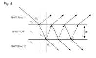
- FIG. 4 is a diagram illustrating paths of light in a thin film that is adjacent to the materials having different refractive indexes.
- FIG. 5 is a graph illustrating wavelength dispersion characteristics of the optical film as described in Example 1.
- FIG. 6 is a graph illustrating wavelength dispersion characteristics of the optical film as described in Example 2.
- FIG. 7 is a graph illustrating wavelength dispersion characteristics of the optical film as described in Example 3.
- FIG. 8 is a graph illustrating wavelength dispersion characteristics of the optical film as described in Example 4.
- FIG. 9 is a graph illustrating wavelength dispersion characteristics of the optical film as described in Example 5.
- FIG. 10 is a graph illustrating retardance in a slow axis as described in Example 6.
- FIG. 11 is a graph illustrating retardance in a slow axis as described in Comparative example 1.
- FIG. 12 is a graph illustrating retardance in a fast axis as described in Example 6.
- FIG. 13 is a graph illustrating retardance in a fast axis as described in Comparative example 1.
- FIG. 14 is a graph illustrating a color compensation effect in installing the optical film according to one exemplary embodiment of the present invention.
- FIG. 15 is a graph illustrating a color compensation effect in installing a conventional optical film.
- FIG. 16 is a graph illustrating a contrast ratio improvement effect in installing the optical film according to one exemplary embodiment of the present invention.
- the optical film according to one exemplary embodiment of the present invention includes at least one retardation film; and at least one isotropic layer made of an isotropic material that is coated or stacked onto the retardation film, wherein the difference in average refractive index between the retardation film and the isotropic layer is at least 0.1 or more, and preferably is in a range from 0.1 to 1.0.
- the optical film according to one exemplary embodiment of the present invention as configured thus has different wavelength dispersion characteristics from the original retardation films since the polarization rotation and thin film interference eclair when light is passed through the isotropic layer.
- FIG. 3 is a diagram illustrating a polarization rotation.
- the light that is incident with an incidence angle to a plane formed by two materials having different refractive indexes is refracted as flitch as the respective differences in refractive index, and some of the incident light is reflected in the same angle as the incidence angle.
- the incident light may have any polarization state.
- the polarization of light that vibrates in a fast axis to the incidence plane is called s-polarization
- the polarization of light that that vibrates in a horizontal direction to the incidence plane is called p-polarization.
- the reflectance (r) and the transmittance (t) according to the s-polarization and the p-polarization may be represented by the following Fresnel equation.
- r s ( n i ⁇ cos ⁇ ⁇ ⁇ i - n f ⁇ cos ⁇ ⁇ ⁇ f ) / ( n i ⁇ cos ⁇ ⁇ ⁇ i + n f ⁇ cos ⁇ ⁇ ⁇ i )
- r p ( n f ⁇ cos ⁇ ⁇ ⁇ i - n i ⁇ cos ⁇ ⁇ ⁇ f ) / ( n f ⁇ cos ⁇ ⁇ ⁇ i + n i ⁇ cos ⁇ ⁇ ⁇ f )
- t s ( 2 ⁇ n i ⁇ cos ⁇ ⁇ ⁇ i ) / ( n i ⁇ cos ⁇ ⁇ ⁇ i + n f ⁇ cos ⁇ ⁇ ⁇ f )
- t p ( 2 ⁇ n i ⁇ cos ⁇ ⁇ ⁇ i )
- r represents a reflectance
- t represents a transmittance
- n i represents a refractive index in a light-incident material
- ⁇ i represents an incidence angle in the light-incident material
- n f represents a refractive index in a light-transmitted material
- ⁇ f represents an incidence angle in the light-transmitted material
- the transmittance and reflectance of each of the p-polarization and s-polarization is a function of a refractive index of a material and an incidence angle of light
- the transmittance and reflectance of the p-polarization and the s-polarization are varied when the refractive index of the material or the incidence angle of light is varied, which leads to the polarization rotation in which a polarization state of light is changed.
- the p-polarization and the s-polarization are different in transmittance when a 45° linearly polarized light with p-polarization and s-polarization that are identical in size is passed through a material layer having different refractive indexes as shown in FIG. 3 , the transmitted light is changed into a linearly polarized light that are different from the original 45° linearly polarized light.
- FIG. 4 is a diagram illustrating interference.
- FIG. 4 shows paths of light in a thin film that is adjacent to the materials having differences in refractive index.
- the light entering the thin film is repeatedly transmitted to or reflected from an interface of the two materials, and the observed light is identical to the sum of the transmitted light and the reflected light.
- This is referred to as ‘thin film interference.’
- the thin film interference causes the changes in phase.
- the present inventors took consideration of the above facts, and found that, when a layer of isotropic materials having different refractive indexes is formed on a retardation film, the change in retardance crows by the thin film interference and the polarization rotation occurs by the differences in transmittance and reflectance of the p-polarization and the s-polarization, which indicates that the wavelength dispersion characteristics of the retardation film may be effectively changed. Therefore, the present invention has been completed on the basis of the above facts. Also, the present inventors have found that the wavelength dispersion characteristics of an optical film may be varied according to the thickness of an isotropic layer, the kinds of isotropic materials, and the kinds of retardation films.
- optical films having a variety of wavelength dispersion characteristics may be manufactured only when an isotropic layer is formed on the conventional retardation films.
- One exemplary embodiment of the present invention is advantageous because the productivity may be considerably improved due to the simple manufacturing processes and the small limitation on the use of materials, compared to the conventional methods.
- the difference in average refractive indexes between the isotropic layer and the retardation film should be at least 0.1 or more, preferably be in a range from approximately 0.1 to 1.0, and more preferably in a range from approximately 0.1 to 0.5 in order to achieve the significant change in wavelength dispersion characteristics.
- the thin film interference more strongly appears as the difference in refractive indexes between a thin film material and its adjacent materials increases, which leads to an increase in the size of retardance caused by the thin film interference.
- the present inventors have found, on the basis of the experiments, that the commercially available change in wavelength dispersion characteristics may be achieved when the retardance should be changed by 1 nm or more, and preferably approximately 3 nm or more when compared to the conventional retardance as measured at wavelengths of 500, 550 and 600 nm.
- the retardance is different but the difference in refractive index between the isotropic layer and the retardation film should be at least 0.1 or more, preferably is in a range from approximately 0.1 to 1.0, and more preferably in a range from approximately 0.1 to 0.5, depending on the thickness of an isotropic layer.
- a retardance value was measured using an Axoscan retardance measurement apparatus.
- the isotropic layer preferably has a thickness of approximately 1 to 500 nm, and more preferably approximately 10 to 300 nm so as to achieve the significant change in wavelength dispersion characteristics.
- the thickness of the isotropic layer is less than 1 nm, there is difficulty in the manufacturing process, whereas when the thickness of the isotropic layer exceeds 500 nm, the front transmittance of the optical films is deteriorated, which adversely affect its optical properties.
- the changes in phase by the thin film interference is not significant when the thickness of a thin film is generally higher than wavelengths of light, but the changes in phase is increased when the thickness of a thin film is smaller than the wavelength of light. Therefore, the thickness of the isotropic layer is preferably smaller than the wavelength of light in order to achieve the significant change in wavelength dispersion characteristics. Considering that a wavelength range of a visible ray is in a range of 400 to 800 nm, the thickness of the isotropic layer according to one exemplary embodiment of the present invention is preferably within the above-mentioned thickness range.
- the expression “retardation film” used herein includes a film, a layer and a plate, all of which have uni-axial or bi-axial birefringence.
- a uni-axial retardation film refers to a film whose refractive index is identical in two of three directions (x, y and z) and is different in one of three directions (x, y and z)
- the bi-axial retardation film refers to a film whose refractive index is different in all three directions (x, y and z).
- all anisotropic films such as a ⁇ A-film, a ⁇ B-film or a ⁇ C-film, having retardance may be used as the retardation film.
- the A-film refers to a film having birefringence in plane, and the retardance value in plane, R in , is defined, as follows.
- R in d ⁇ ( n e ⁇ n o )
- n e represents one of three refractive indexes
- n o represents two identical refractive indexes
- d represents a thickness of a film.
- Film A is generally manufactured by elongating a polymeric film in a uni-axial direction, or arranging rod-type or discotic liquid crystal in a horizontal direction.
- Film C is a film having different refractive indexes in a thickness direction (z axis), and the retardance in thickness direction, R th , is defined, as follows.
- R in d ⁇ ( n z ⁇ n y )
- n z represents a refractive index in a thickness direction
- n y represents a refractive index in an in-plane direction
- d represents a thickness.
- Film C is generally manufactured by elongating a polymeric film in a uni-axial direction, or by arranging a rod-type or discotic liquid crystal in a fast axis.
- Film B is a film having different refractive indexes in all three directions, and the retardance value in plane, R in , and the retardance value in thickness direction, R th , are defined, as follows.
- R in d ⁇ ( n x ⁇ n y )
- R th d ⁇ ( n z ⁇ n y )
- the film B becomes a ⁇ B film when the film B satisfies nx>ny>nz, and the film B becomes a +B film when the film B satisfies nx>nz>ny.
- the B film is manufactured by elongating a polymeric film in a bi-axial direction.
- triacetylcellulose (TAC), cyclic olefin polymer (COP) or the like may be used as the polymeric film.
- the isotropic material is characterized in that it has a refractive index from which the difference in average refractive index of the retardation film is at least 0.1 or more. That is, when a retardation film has an average refractive index of 1.5, isotropic materials having a refractive index of 1.4 or less or 1.6 or more may be used as the retardation film.
- the average refractive index of the retardation film means (n x +n y +n z )/3.
- the isotropic material used in the present invention includes, but is not particularly limited to, isotropic materials, such as ITO, ZnS and TiO 2 , having a higher refractive index (high refractive index) than the average refractive index of the retardation film, and isotropic materials, such as silicone-modified fluoropolymer, silicone and porous silica nano-molecules, having a lower refractive index (low refractive index) than the average refractive index of the retardation film, and they may be used alone or in combinations thereof.
- isotropic materials such as ITO, ZnS and TiO 2 , having a higher refractive index (high refractive index) than the average refractive index of the retardation film
- isotropic materials such as silicone-modified fluoropolymer, silicone and porous silica nano-molecules, having a lower refractive index (low refractive index) than the average refractive index of the retardation film, and they may be used alone or in combinations thereof.
- silicone-modified fluoropolymer examples include US Patent Publication No. 2006-0148824, and a silicon (i.e. LSS-2233-10-PST (Polymer Systems Technology Limited)) having a refractive index of approximately 1.28 to 1.33 may be used as the silicon. Also, a product having a refractive index of approximately 1.25 to 1.3 (commercially available from Merck) may be used as the porous silica nano-molecules.
- any of materials having a refractive index so that the difference in average refractive index between the retardation film and the isotropic layer can be 0.1 or more and having isotropic property may be used as the materials constituting the isotropic layer.
- each of the retardation film and the isotropic layer may be stacked in plural number.
- the method for adjusting wavelength dispersion characteristics of an optical film according to one exemplary embodiment of the present invention is carried out by forming an isotropic layer onto a retardation film, wherein the isotropic material has a refractive index so that the difference in average refractive index between the retardation film and the isotropic layer is 0.1 or more, and the retardation film has its own inherent wavelength dispersion characteristics.
- a film, a layer and a plate, all of which have uni-axial or bi-axial birefringence may be used as the retardation film, and examples of the retardation film include, for example, a ⁇ A-film, a ⁇ B-film or a ⁇ C-film.
- the isotropic layer includes isotropic materials, such as ITO, ZnS and TiO 2 , having a higher refractive index (high refractive index) than the average refractive index of the retardation film, and isotropic materials, such as silicone-modified fluoropolymer, silicone and porous silica nano-molecules, having a lower refractive index (low refractive index) than the average refractive index of the retardation film.
- isotropic materials such as ITO, ZnS and TiO 2 , having a higher refractive index (high refractive index) than the average refractive index of the retardation film
- isotropic materials such as silicone-modified fluoropolymer, silicone and porous silica nano-molecules, having a lower refractive index (low refractive index) than the average refractive index of the retardation film.
- the stacking process may be carried out using a sputtering, coating or chemical vapor deposition method.
- the stacking process should be performed without degrading the optical characteristics (transmittance, etc.) of the retardation film, and therefore it is preferred to select and use a suitable method according to the kinds of the stacked isotropic materials.
- the sputtering method is preferably used when ITO is stacked onto the retardation film
- the coating method is preferably used when titanium dioxide (TiO 2 ) is staked onto the retardation film.
- the changes in phase occur by the polarization rotation and the thin film interference that are caused by the difference in transmittance and reflectance of the p-polarization and the s-polarization in an interface of the retardation film and the isotropic material, and therefore the wavelength dispersion characteristics of the optical films are different from those of the original retardation film.
- the changes in wavelength dispersion characteristics are varied according to the thickness of an isotropic layer, and the difference in refractive indexes between the isotropic layer and the retardation film. It is considered that an optical film having desired wavelength dispersion characteristics may be manufactured through the context and suitable experiments disclosed in this specification, for example, by coating a retardation film with isotropic layers having different thicknesses and determining wavelength dispersion characteristics of the retardation film, as evident to those skilled in the art.
- the method according to one exemplary embodiment of the present invention as configured thus may be used to manufacture an optical film having optimized wavelength dispersion characteristics, depending on the desired purposes and uses, for example, modes (IPS, TN and the like) of LCD devices.
- IPS modes
- TN TN
- the optical film having optimized wavelength dispersion characteristics is installed in a display device, it is possible to manufacture the display device having excellent color lams and contrast ratio when compared to the conventional display devices.
- TAC films having a refractive index of 1.48 and a thickness of 80 ⁇ m were coated respectively with TiO 2 having a refractive index of approximately 1.68 to thicknesses of 36 nm, 60 nm, 88 nm and 116 nm, and then aired to form isotropic layers, thus to prepare optical films.
- an optical film in which a 36 nm-thick isotropic layer is formed is referred to as A 1
- an optical film in which a 60 nm-thick isotropic layer is formed is referred to as B 1
- an optical film in which an 88 nm-thick isotropic layer is formed is referred to as C 1
- an optical film in which a 116 nm-thick isotropic layer is formed is referred to as D 1 .
- Wavelength dispersion characteristics R( ⁇ )/R (550 nm) of the optical films A 1 , B 1 , C 1 and D 1 were measured under conditions of a reference wavelength of 550 nm and a tilt angle of 40°.
- the wavelength dispersion characteristics were measured using a retardance measurement apparatus (Axoscan, Axometrics Co. Ltd.).
- the measured wavelength range is determined to be in a range from 400 to 800 nm, and the measured retardance values according to the wavelength are divided by the retardance value at 550 nm, and the resulting value is then expressed as the dispersion characteristics.
- the measured results are shown in FIG. 5 .
- an optical film in which a 38 nm-thick isotropic layer is formed is referred to as A 2
- an optical film in which a 61 nm-thick isotropic layer is formed is referred to as B 2
- an optical film in which a 90 nm-thick isotropic layer is formed is referred to as C 2
- an optical film in which a 115 nm-thick isotropic layer is formed is referred to as D 2 .
- Wavelength dispersion characteristics R( ⁇ )/R (550 nm) of the optical films A 2 , B 2 , C 2 and D 2 were measured under conditions of a reference wavelength of 550 nm and a tilt angle of 40° in the same manner as in Example 1. The measured results are shown in FIG. 6 .
- Three positive uni-axial COP films (+A films, commercially available from Zeon) having a refractive index of 1.53 and a thickness of 80 ⁇ m were sputtered respectively with ITO having a refractive index of approximately 2.00 to form isotropic layers having thicknesses of 80 nm, 120 nm and 160 nm, respectively, thus to prepare optical films.
- an optical film in which an 80 nm-thick isotropic layer is formed is referred to as A 3
- an optical film in which a 120 nm-thick isotropic layer is formed is referred to as B 3
- an optical film in which a 160 nm-thick isotropic layer is formed is referred to as C 3 .
- Wavelength dispersion characteristics R( ⁇ )/R(550 nm) of the optical films A 3 , B 3 and C 3 were measured under conditions of a reference wavelength of 550 nm and a tilt angle of 40° in the same manner as in Example 1. The measured results are shown in FIG. 7 .
- Wavelength dispersion characteristics R( ⁇ )/R (550 nm) of the A 4 were measured under conditions of a reference wavelength of 550 nm and a tilt angle of 40° in the same manner as in Example 1. The measured results are shown in FIG. 8 .
- an optical film in which a 40 nm-thick isotropic layer is formed is referred to as A 5
- an optical film in which an 86 nm-thick isotropic layer is formed is referred to as B 5
- an optical film in which a 144 nm-thick isotropic layer is formed is referred to as C 5 .
- Wavelength dispersion characteristics R( ⁇ )/R (550 nm) of the optical films A 5 , B 5 and C 5 were measured under conditions of a reference wavelength of 550 nm and a tilt angle of 40° in the same manner as in Example 1. The measured results are shown in FIG. 9 .
- the optical films according to the present invention shows a variety of wavelength dispersion characteristics, depending on the kinds of the retardation film, the thickness of the isotropic materials, and the thickness of films.
- TAC films having a refractive index of 1.48 and a thickness of 80 ⁇ m were coated respectively with TiO 2 having a refractive index of approximately 1.82 to thicknesses of 20 nm, 70 nm and 130 nm, and then cared to form isotropic layers, thus to prepare optical films.
- an isotropic layer was formed on each of the TAC films to prepare optical films.
- an optical film in which a 20 nm-thick isotropic layer is formed is referred to as A 6
- an optical film in which a 70 nm-thick isotropic layer is formed is referred to as B 6
- an optical film in which a 130 nm-thick isotropic layer is formed is referred to as C 6 .
- TAC films ( ⁇ B films, commercially available from Fuji) having the same refractive index and thickness were coated respectively with an acrylate resin having a refractive index of approximately 1.52 to thicknesses of 20 nm, 70 nm and 130 nm, and then cured. Then, an isotropic layer was formed on each of the TAC films to prepare optical films.
- an optical film in which a 20 nm-thick isotropic layer is formed is referred to as A 7
- an optical film in which a 70 nm-thick isotropic layer is formed is referred to as B 7
- an optical film in which a 130 nm-thick isotropic layer is formed is referred to as C 7 .
- Each of the optical films of Example 6 and Comparative example 1 were measured for retardance in a slow axis.
- the retardance of the optical films was measured under conditions of a reference wavelength of 550 nm and a tilt angle of 50°.
- the wavelength dispersion characteristics were measured using a retardance measurement apparatus (Axoscan, Axometrics Co. Ltd.), and a measured wavelength range was 500 to 650 nm.
- the measured results are shown in FIG. 10 (Example 6) and FIG. 11 (Comparative example 1).
- Each of the optical films of Example 6 and Comparative example 1 were measured for retardance in a fast axis.
- the retardance of the optical films was measured under conditions of a reference wavelength of 550 nm and a tilt angle of 50°.
- the wavelength dispersion characteristics were measured using a retardance measurement apparatus (Axoscan, Axometrics Co. Ltd.), and a measured wavelength range was 500 to 650 nm.
- the measured results are shown in FIG. 12 (Example 6) and FIG. 13 (Comparative example 1).
- TAC film ( ⁇ B film, commercially available from Fuji) having a refractive index of 1.48 and a thickness of 80 ⁇ m was coated with a TiO 2 -based reactive solution having a refractive index of approximately 1.83 to a thickness of 50 nm to prepare an optical film.
- the optical film as prepared thus was installed in a direct-type backlight unit (CMO), and a color locus of the optical film was measured.
- the measurement of the color locus was performed, using an Eldim measurement apparatus, by measuring a black color and measuring a color laws of the optical film at a tilt angle of 50° in all directions. The measured results are shown in FIG. 14 .
- the ⁇ B film (commercially available from Fuji) as described right above was installed in a backlight unit, and a color locus of the optical film was measured as the same manner as described right above. The measured results are shown in FIG. 15 .
- the backlight unit has excellent color laws, compared to the conventional backlight unit having only the ⁇ B retardation film installed therein.
- TAC film ( ⁇ B film, commercially available from Fuji) having a refractive index of 1.48 and a thickness of 80 ⁇ m was (Dated with a TiO 2 -based reactive solution having a refractive index of approximately 1.83 to a thickness of 50 nm to prepare an optical film.
- the optical film as prepared thus was installed in a direct-type backlight unit (CMO), and a black luminance of the optical film was measured.
- CMO direct-type backlight unit
- the ⁇ B film (commercially available from Fuji) as described right above was installed in a backlight unit, and a black luminance of the optical film was measured as the same manner as described right above.
- a solid line represents a line when the optical film according to one exemplary embodiment of the present invention is installed in a backlight unit
- a dotted lone represents a line when the convention ⁇ B retardation film is installed in a backlight unit.
- the backlight unit has a significantly reduced black luminance when the optical film according to one exemplary embodiment of the present invention is used in the backlight unit, which indicates that the contrast ratio of the optical film is improved.
Landscapes
- Physics & Mathematics (AREA)
- General Physics & Mathematics (AREA)
- Optics & Photonics (AREA)
- Polarising Elements (AREA)
- Liquid Crystal (AREA)
Abstract
Description
R in =d×(n e −n o)
R in =d×(n z −n y)
R in =d×(n x −n y)
R th =d×(n z −n y)
Claims (4)
Priority Applications (1)
| Application Number | Priority Date | Filing Date | Title |
|---|---|---|---|
| US14/273,146 US9448349B2 (en) | 2007-08-14 | 2014-05-08 | Optical film and method of adjusting wavelength dispersion characteristics of the same |
Applications Claiming Priority (7)
| Application Number | Priority Date | Filing Date | Title |
|---|---|---|---|
| KR20070081943 | 2007-08-14 | ||
| KR10-2007-0081943 | 2007-08-14 | ||
| KR1020080079275A KR100964964B1 (en) | 2007-08-14 | 2008-08-13 | How to adjust wavelength dispersion characteristics of optical film and optical film |
| PCT/KR2008/004715 WO2009022863A2 (en) | 2007-08-14 | 2008-08-13 | Optical film and method of manufacturing the same |
| KR10-2008-0079275 | 2008-08-13 | ||
| US44888009A | 2009-07-13 | 2009-07-13 | |
| US14/273,146 US9448349B2 (en) | 2007-08-14 | 2014-05-08 | Optical film and method of adjusting wavelength dispersion characteristics of the same |
Related Parent Applications (2)
| Application Number | Title | Priority Date | Filing Date |
|---|---|---|---|
| PCT/KR2008/004715 Division WO2009022863A2 (en) | 2007-08-14 | 2008-08-13 | Optical film and method of manufacturing the same |
| US12/448,880 Division US8767297B2 (en) | 2007-08-14 | 2008-08-13 | Optical film and method of adjusting wavelength dispersion characteristics of the same |
Publications (2)
| Publication Number | Publication Date |
|---|---|
| US20140240830A1 US20140240830A1 (en) | 2014-08-28 |
| US9448349B2 true US9448349B2 (en) | 2016-09-20 |
Family
ID=40686231
Family Applications (2)
| Application Number | Title | Priority Date | Filing Date |
|---|---|---|---|
| US12/448,880 Active US8767297B2 (en) | 2007-08-14 | 2008-08-13 | Optical film and method of adjusting wavelength dispersion characteristics of the same |
| US14/273,146 Active US9448349B2 (en) | 2007-08-14 | 2014-05-08 | Optical film and method of adjusting wavelength dispersion characteristics of the same |
Family Applications Before (1)
| Application Number | Title | Priority Date | Filing Date |
|---|---|---|---|
| US12/448,880 Active US8767297B2 (en) | 2007-08-14 | 2008-08-13 | Optical film and method of adjusting wavelength dispersion characteristics of the same |
Country Status (7)
| Country | Link |
|---|---|
| US (2) | US8767297B2 (en) |
| EP (1) | EP2179311B1 (en) |
| JP (1) | JP2010537227A (en) |
| KR (1) | KR100964964B1 (en) |
| CN (1) | CN101617249B (en) |
| TW (1) | TWI375094B (en) |
| WO (1) | WO2009022863A2 (en) |
Families Citing this family (16)
| Publication number | Priority date | Publication date | Assignee | Title |
|---|---|---|---|---|
| EP2179311B1 (en) * | 2007-08-14 | 2015-09-16 | LG Chem, Ltd. | Optical film and method of manufacturing the same |
| KR101314480B1 (en) * | 2008-12-26 | 2013-10-07 | 주식회사 엘지화학 | Polarizer for ips mode lcd and ips mode lcd comprising the same |
| US9234987B2 (en) * | 2010-09-24 | 2016-01-12 | Akron Polymer Systems, Inc. | Wide-view multilayer optical films |
| JP5062385B1 (en) * | 2011-02-28 | 2012-10-31 | 日本ゼオン株式会社 | Multi-layer film and method for producing multi-layer film |
| KR101401050B1 (en) * | 2013-08-09 | 2014-06-27 | 동우 화인켐 주식회사 | Touch sensing electrode and touch screen panel comprising the same |
| KR101666702B1 (en) * | 2013-09-30 | 2016-10-17 | 주식회사 엘지화학 | Retadation film and preparing method for retadation film |
| WO2015050374A1 (en) * | 2013-10-01 | 2015-04-09 | 주식회사 엘지화학 | Optical film |
| JP6304664B2 (en) * | 2013-10-01 | 2018-04-04 | エルジー・ケム・リミテッド | Optical film, composite polarizing plate including the same, and liquid crystal display |
| KR20150058028A (en) * | 2013-11-20 | 2015-05-28 | 동우 화인켐 주식회사 | Hibride touch sensing electrode and touch screen panel comprising the same |
| KR101444132B1 (en) * | 2013-11-20 | 2014-11-04 | 동우 화인켐 주식회사 | Touch sensing electrode combined with complexed polarization plate and touch screen panel comprising the same |
| US10376309B2 (en) | 2016-08-02 | 2019-08-13 | Covidien Lp | Ablation cable assemblies and a method of manufacturing the same |
| US11197715B2 (en) | 2016-08-02 | 2021-12-14 | Covidien Lp | Ablation cable assemblies and a method of manufacturing the same |
| US11065053B2 (en) | 2016-08-02 | 2021-07-20 | Covidien Lp | Ablation cable assemblies and a method of manufacturing the same |
| KR102444973B1 (en) | 2019-06-19 | 2022-09-19 | 삼성에스디아이 주식회사 | Polarizing plate and optical display including same |
| JP7448939B2 (en) * | 2020-03-10 | 2024-03-13 | 東海光学株式会社 | Delay mirror and delay mirror system |
| CN113687544A (en) * | 2020-05-18 | 2021-11-23 | 京东方科技集团股份有限公司 | Display panel, preparation method thereof and display device |
Citations (26)
| Publication number | Priority date | Publication date | Assignee | Title |
|---|---|---|---|---|
| US3799653A (en) | 1972-04-26 | 1974-03-26 | Bippon Kogaku Kk | Multi-layer anti-reflection coating |
| JPH02256023A (en) | 1988-11-04 | 1990-10-16 | Fuji Photo Film Co Ltd | Liquid crystal display device |
| US5189538A (en) | 1988-11-04 | 1993-02-23 | Fuji Photo Film Co., Ltd. | Liquid crystal display having positive and negative birefringent compensator films |
| US5396355A (en) | 1991-06-17 | 1995-03-07 | Seiko Epson Corporation | Optically compensating film, optical compensator and liquid crystal display |
| JPH0798411A (en) | 1993-09-28 | 1995-04-11 | Fuji Photo Film Co Ltd | Optical compensation film |
| JP2609139B2 (en) | 1988-10-31 | 1997-05-14 | 日東電工株式会社 | Laminated retarder |
| DE10033916A1 (en) | 1999-09-17 | 2001-03-22 | Merck Patent Gmbh | Circular polarizer used in liquid crystal displays has a layer made of an optical anisotropic material and a layer made of an optical isotropic layer |
| EP1103885A1 (en) | 1998-06-18 | 2001-05-30 | Kaneka Corporation | Transparent touch panel and liquid crystal display with transparent touch panel |
| US6361838B1 (en) | 1999-02-08 | 2002-03-26 | Nitto Denko Corporation | Optical film, optical member and optical element |
| US6498683B2 (en) * | 1999-11-22 | 2002-12-24 | 3M Innovative Properties Company | Multilayer optical bodies |
| JP2003098348A (en) | 2001-09-21 | 2003-04-03 | Konica Corp | Polarizing plate and liquid crystal display device using the same |
| US20040080693A1 (en) | 2000-07-21 | 2004-04-29 | Konica Corporation | Optical compensation sheet and liquid crystal display |
| US6800697B2 (en) | 2000-04-24 | 2004-10-05 | Teijin Limited | Process for producing retardation film |
| JP2004287109A (en) | 2003-03-24 | 2004-10-14 | Konica Minolta Holdings Inc | Phase-contrast film, method for manufacturing the same, polarizing plate, and display device |
| US20050014913A1 (en) | 2002-11-22 | 2005-01-20 | Won-Kook Kim | Negative c-plate type optical anisotropic film comprising poly cycloolefin and method for preparing the same |
| US20050123693A1 (en) | 2002-04-19 | 2005-06-09 | Yoji Ito | Optical compensatory sheet comprising polymer film |
| US20060105115A1 (en) * | 2004-11-16 | 2006-05-18 | Keiji Kashima | Retardation film and method for producing the same, optical functional film, polarizing film, and display device |
| JP2006154837A (en) | 2005-12-13 | 2006-06-15 | Dainippon Printing Co Ltd | Antireflection film |
| WO2006068216A1 (en) | 2004-12-24 | 2006-06-29 | Matsushita Electric Works, Ltd. | Liquid crystal display |
| US20060147724A1 (en) | 2004-12-30 | 2006-07-06 | 3M Innovative Properties Company | Low refractive index coating composition for use in antireflection polymer film coatings and manufacturing method |
| US20060188664A1 (en) | 2005-02-21 | 2006-08-24 | Fuji Photo Film Co., Ltd. | Coating composition for the formation of low refractive index layer, antireflection film, polarizing plate and liquid crystal display device |
| WO2007029788A1 (en) | 2005-09-09 | 2007-03-15 | Nitto Denko Corporation | Polarizing plate with optical compensation layer, liquid crystal panel using polarizing plate with optical compensation layer, and image display unit |
| JP2007098411A (en) | 2005-09-30 | 2007-04-19 | Mitsui High Tec Inc | Rotary-type punching device and punching method of metal plate |
| JP2007133172A (en) | 2005-11-10 | 2007-05-31 | Nippon Telegr & Teleph Corp <Ntt> | Steady mode excitation device |
| US8767297B2 (en) * | 2007-08-14 | 2014-07-01 | Lg Chem, Ltd. | Optical film and method of adjusting wavelength dispersion characteristics of the same |
| US20150153497A1 (en) * | 2013-10-01 | 2015-06-04 | Lg Chem, Ltd. | Optical film |
Family Cites Families (10)
| Publication number | Priority date | Publication date | Assignee | Title |
|---|---|---|---|---|
| US1264568A (en) | 1913-12-23 | 1918-04-30 | Rail Joint Co | Rail-joint. |
| US4446305A (en) * | 1981-03-02 | 1984-05-01 | Polaroid Corporation | Optical device including birefringent polymer |
| JP3313406B2 (en) | 1991-06-17 | 2002-08-12 | セイコーエプソン株式会社 | Retardation film, retardation plate and liquid crystal display |
| CA2179625C (en) * | 1993-12-21 | 2004-10-26 | Andrew J. Ouderkirk | Optical polarizer |
| JP2000112663A (en) * | 1997-11-27 | 2000-04-21 | Kanegafuchi Chem Ind Co Ltd | Transparent touch panel and liquid crystal cell with transparent touch panel |
| JP4077318B2 (en) | 2000-12-20 | 2008-04-16 | 株式会社クラレ | Process for producing saponified ethylene-vinyl acetate copolymer |
| JP2006276697A (en) | 2005-03-30 | 2006-10-12 | Dainippon Printing Co Ltd | Retardation film and liquid crystal display device |
| JP2007094271A (en) | 2005-09-30 | 2007-04-12 | Dainippon Printing Co Ltd | Retardation layer forming coating liquid, retardation optical laminate, and method for producing retardation optical laminate |
| TWI276852B (en) * | 2005-11-07 | 2007-03-21 | Yi-Jiun Ren | Optical configuration for generating polarization conversion |
| KR100907818B1 (en) * | 2006-06-08 | 2009-07-16 | 주식회사 엘지화학 | An integrated O-film for improving the TN-LCD viewing angle, a polarizing plate laminate containing the same, and a TN-LCD |
-
2008
- 2008-08-13 EP EP08793229.9A patent/EP2179311B1/en active Active
- 2008-08-13 KR KR1020080079275A patent/KR100964964B1/en active Active
- 2008-08-13 US US12/448,880 patent/US8767297B2/en active Active
- 2008-08-13 WO PCT/KR2008/004715 patent/WO2009022863A2/en not_active Ceased
- 2008-08-13 JP JP2010520942A patent/JP2010537227A/en active Pending
- 2008-08-13 CN CN200880002311.4A patent/CN101617249B/en active Active
- 2008-08-14 TW TW097130935A patent/TWI375094B/en active
-
2014
- 2014-05-08 US US14/273,146 patent/US9448349B2/en active Active
Patent Citations (30)
| Publication number | Priority date | Publication date | Assignee | Title |
|---|---|---|---|---|
| US3799653A (en) | 1972-04-26 | 1974-03-26 | Bippon Kogaku Kk | Multi-layer anti-reflection coating |
| JP2609139B2 (en) | 1988-10-31 | 1997-05-14 | 日東電工株式会社 | Laminated retarder |
| JPH02256023A (en) | 1988-11-04 | 1990-10-16 | Fuji Photo Film Co Ltd | Liquid crystal display device |
| US5189538A (en) | 1988-11-04 | 1993-02-23 | Fuji Photo Film Co., Ltd. | Liquid crystal display having positive and negative birefringent compensator films |
| US5396355A (en) | 1991-06-17 | 1995-03-07 | Seiko Epson Corporation | Optically compensating film, optical compensator and liquid crystal display |
| JPH0798411A (en) | 1993-09-28 | 1995-04-11 | Fuji Photo Film Co Ltd | Optical compensation film |
| EP1103885A1 (en) | 1998-06-18 | 2001-05-30 | Kaneka Corporation | Transparent touch panel and liquid crystal display with transparent touch panel |
| US6411344B2 (en) | 1998-06-18 | 2002-06-25 | Kaneka Corporation | Transparent touch panel and liquid crystal display device equipped with transparent touch panel |
| US6361838B1 (en) | 1999-02-08 | 2002-03-26 | Nitto Denko Corporation | Optical film, optical member and optical element |
| GB2355315B (en) | 1999-09-17 | 2003-10-08 | Merck Patent Gmbh | Circular polarizer with optically anisotropic and isotropic layers |
| DE10033916A1 (en) | 1999-09-17 | 2001-03-22 | Merck Patent Gmbh | Circular polarizer used in liquid crystal displays has a layer made of an optical anisotropic material and a layer made of an optical isotropic layer |
| US6498683B2 (en) * | 1999-11-22 | 2002-12-24 | 3M Innovative Properties Company | Multilayer optical bodies |
| US6800697B2 (en) | 2000-04-24 | 2004-10-05 | Teijin Limited | Process for producing retardation film |
| US20040080693A1 (en) | 2000-07-21 | 2004-04-29 | Konica Corporation | Optical compensation sheet and liquid crystal display |
| JP2003098348A (en) | 2001-09-21 | 2003-04-03 | Konica Corp | Polarizing plate and liquid crystal display device using the same |
| US20050123693A1 (en) | 2002-04-19 | 2005-06-09 | Yoji Ito | Optical compensatory sheet comprising polymer film |
| TWI264568B (en) | 2002-04-19 | 2006-10-21 | Fuji Photo Film Co Ltd | Optical compensatory sheet comprising polymer film |
| US20050014913A1 (en) | 2002-11-22 | 2005-01-20 | Won-Kook Kim | Negative c-plate type optical anisotropic film comprising poly cycloolefin and method for preparing the same |
| JP2004287109A (en) | 2003-03-24 | 2004-10-14 | Konica Minolta Holdings Inc | Phase-contrast film, method for manufacturing the same, polarizing plate, and display device |
| US20060105115A1 (en) * | 2004-11-16 | 2006-05-18 | Keiji Kashima | Retardation film and method for producing the same, optical functional film, polarizing film, and display device |
| WO2006068216A1 (en) | 2004-12-24 | 2006-06-29 | Matsushita Electric Works, Ltd. | Liquid crystal display |
| US20060147724A1 (en) | 2004-12-30 | 2006-07-06 | 3M Innovative Properties Company | Low refractive index coating composition for use in antireflection polymer film coatings and manufacturing method |
| US20060188664A1 (en) | 2005-02-21 | 2006-08-24 | Fuji Photo Film Co., Ltd. | Coating composition for the formation of low refractive index layer, antireflection film, polarizing plate and liquid crystal display device |
| WO2007029788A1 (en) | 2005-09-09 | 2007-03-15 | Nitto Denko Corporation | Polarizing plate with optical compensation layer, liquid crystal panel using polarizing plate with optical compensation layer, and image display unit |
| EP1930750A1 (en) | 2005-09-09 | 2008-06-11 | Nitto Denko Corporation | Polarizing plate with optical compensation layer, liquid crystal panel using polarizing plate with optical compensation layer, and image display unit |
| JP2007098411A (en) | 2005-09-30 | 2007-04-19 | Mitsui High Tec Inc | Rotary-type punching device and punching method of metal plate |
| JP2007133172A (en) | 2005-11-10 | 2007-05-31 | Nippon Telegr & Teleph Corp <Ntt> | Steady mode excitation device |
| JP2006154837A (en) | 2005-12-13 | 2006-06-15 | Dainippon Printing Co Ltd | Antireflection film |
| US8767297B2 (en) * | 2007-08-14 | 2014-07-01 | Lg Chem, Ltd. | Optical film and method of adjusting wavelength dispersion characteristics of the same |
| US20150153497A1 (en) * | 2013-10-01 | 2015-06-04 | Lg Chem, Ltd. | Optical film |
Also Published As
| Publication number | Publication date |
|---|---|
| EP2179311A2 (en) | 2010-04-28 |
| KR20090017437A (en) | 2009-02-18 |
| WO2009022863A3 (en) | 2009-04-16 |
| CN101617249B (en) | 2014-07-09 |
| US20100134910A1 (en) | 2010-06-03 |
| TW200916918A (en) | 2009-04-16 |
| TWI375094B (en) | 2012-10-21 |
| US8767297B2 (en) | 2014-07-01 |
| JP2010537227A (en) | 2010-12-02 |
| EP2179311B1 (en) | 2015-09-16 |
| EP2179311A4 (en) | 2011-08-24 |
| US20140240830A1 (en) | 2014-08-28 |
| CN101617249A (en) | 2009-12-30 |
| WO2009022863A2 (en) | 2009-02-19 |
| KR100964964B1 (en) | 2010-06-21 |
Similar Documents
| Publication | Publication Date | Title |
|---|---|---|
| US9448349B2 (en) | Optical film and method of adjusting wavelength dispersion characteristics of the same | |
| US11604379B2 (en) | Liquid crystal display device and polarizing plate | |
| US10073297B2 (en) | Liquid crystal display having a narrow viewing mode | |
| CN100376984C (en) | Compensation device and compensation method suitable for liquid crystal display | |
| KR101436441B1 (en) | Antireflective polarizing plate and image display apparatus comprising the same | |
| TWI665473B (en) | Optical filter for anti-reflection and organic light-emitting device | |
| EP2024766B1 (en) | Integrated o film for improving viewing angle of tn-lcd, and polarizer plate and tn-lcd including the same | |
| US10018760B2 (en) | Optical film | |
| US8508696B2 (en) | Polarizing plate and display apparatus having the same | |
| TW201825934A (en) | Optical filter for anti-reflection and organic light-emitting device | |
| TWI495911B (en) | Coupled polarizing plate set and blue phase liquid crystal mode liquid crystal display including the same | |
| KR102369639B1 (en) | Display Device | |
| CN101910927B (en) | Liquid crystal display device and substrate for display device | |
| WO2012133155A1 (en) | Liquid crystal display device | |
| KR20080059832A (en) | Display | |
| TWI495910B (en) | Coupled polarizing plate set and blue phase liquid crystal mode liquid crystal display including the same | |
| KR100759158B1 (en) | Polarizer | |
| KR20200105215A (en) | Polarizing Plate | |
| WO2012133140A1 (en) | Liquid crystal display device |
Legal Events
| Date | Code | Title | Description |
|---|---|---|---|
| AS | Assignment |
Owner name: LG CHEM, LTD., KOREA, REPUBLIC OF Free format text: ASSIGNMENT OF ASSIGNORS INTEREST;ASSIGNORS:CHAE, SEUNG HUN;SERGEY, BELYAEV;JEON, BYOUNG KUN;AND OTHERS;REEL/FRAME:032852/0781 Effective date: 20090610 |
|
| STCF | Information on status: patent grant |
Free format text: PATENTED CASE |
|
| FEPP | Fee payment procedure |
Free format text: PAYOR NUMBER ASSIGNED (ORIGINAL EVENT CODE: ASPN); ENTITY STATUS OF PATENT OWNER: LARGE ENTITY |
|
| MAFP | Maintenance fee payment |
Free format text: PAYMENT OF MAINTENANCE FEE, 4TH YEAR, LARGE ENTITY (ORIGINAL EVENT CODE: M1551); ENTITY STATUS OF PATENT OWNER: LARGE ENTITY Year of fee payment: 4 |
|
| MAFP | Maintenance fee payment |
Free format text: PAYMENT OF MAINTENANCE FEE, 8TH YEAR, LARGE ENTITY (ORIGINAL EVENT CODE: M1552); ENTITY STATUS OF PATENT OWNER: LARGE ENTITY Year of fee payment: 8 |
|
| AS | Assignment |
Owner name: SHANJIN OPTOELECTRONICS (SUZHOU) CO., LTD., CHINA Free format text: ASSIGNMENT OF ASSIGNORS INTEREST;ASSIGNOR:LG CHEM LTD.;REEL/FRAME:070629/0281 Effective date: 20250317 |