US9444402B2 - High frequency integrated circuit and device using same - Google Patents
High frequency integrated circuit and device using same Download PDFInfo
- Publication number
- US9444402B2 US9444402B2 US14/846,601 US201514846601A US9444402B2 US 9444402 B2 US9444402 B2 US 9444402B2 US 201514846601 A US201514846601 A US 201514846601A US 9444402 B2 US9444402 B2 US 9444402B2
- Authority
- US
- United States
- Prior art keywords
- terminal
- amplifier
- transistor
- high frequency
- oscillator
- Prior art date
- Legal status (The legal status is an assumption and is not a legal conclusion. Google has not performed a legal analysis and makes no representation as to the accuracy of the status listed.)
- Expired - Fee Related
Links
- 238000012360 testing method Methods 0.000 claims abstract description 179
- 230000001939 inductive effect Effects 0.000 claims abstract description 44
- 230000005540 biological transmission Effects 0.000 claims description 31
- 238000004891 communication Methods 0.000 claims description 7
- 239000003990 capacitor Substances 0.000 description 20
- 238000010586 diagram Methods 0.000 description 19
- 230000003247 decreasing effect Effects 0.000 description 10
- 230000000694 effects Effects 0.000 description 9
- 230000010355 oscillation Effects 0.000 description 6
- 230000003071 parasitic effect Effects 0.000 description 6
- 230000007423 decrease Effects 0.000 description 4
- 238000001514 detection method Methods 0.000 description 4
- 238000007689 inspection Methods 0.000 description 4
- 238000012986 modification Methods 0.000 description 4
- 230000004048 modification Effects 0.000 description 4
- 230000009467 reduction Effects 0.000 description 4
- 230000003252 repetitive effect Effects 0.000 description 4
- 238000006243 chemical reaction Methods 0.000 description 3
- 230000003321 amplification Effects 0.000 description 2
- 238000005516 engineering process Methods 0.000 description 2
- 238000002955 isolation Methods 0.000 description 2
- 238000012544 monitoring process Methods 0.000 description 2
- 238000003199 nucleic acid amplification method Methods 0.000 description 2
- NRNCYVBFPDDJNE-UHFFFAOYSA-N pemoline Chemical compound O1C(N)=NC(=O)C1C1=CC=CC=C1 NRNCYVBFPDDJNE-UHFFFAOYSA-N 0.000 description 2
- 238000012545 processing Methods 0.000 description 2
- 238000010998 test method Methods 0.000 description 2
- 206010039203 Road traffic accident Diseases 0.000 description 1
- XUIMIQQOPSSXEZ-UHFFFAOYSA-N Silicon Chemical compound [Si] XUIMIQQOPSSXEZ-UHFFFAOYSA-N 0.000 description 1
- 238000010276 construction Methods 0.000 description 1
- 230000003412 degenerative effect Effects 0.000 description 1
- 238000012217 deletion Methods 0.000 description 1
- 230000037430 deletion Effects 0.000 description 1
- 238000001914 filtration Methods 0.000 description 1
- 230000006872 improvement Effects 0.000 description 1
- 238000004377 microelectronic Methods 0.000 description 1
- 230000002265 prevention Effects 0.000 description 1
- 239000000523 sample Substances 0.000 description 1
- 230000035945 sensitivity Effects 0.000 description 1
- 229910052710 silicon Inorganic materials 0.000 description 1
- 239000010703 silicon Substances 0.000 description 1
- 239000000758 substrate Substances 0.000 description 1
- 238000013519 translation Methods 0.000 description 1
Images


Classifications
-
- H—ELECTRICITY
- H03—ELECTRONIC CIRCUITRY
- H03B—GENERATION OF OSCILLATIONS, DIRECTLY OR BY FREQUENCY-CHANGING, BY CIRCUITS EMPLOYING ACTIVE ELEMENTS WHICH OPERATE IN A NON-SWITCHING MANNER; GENERATION OF NOISE BY SUCH CIRCUITS
- H03B5/00—Generation of oscillations using amplifier with regenerative feedback from output to input
- H03B5/20—Generation of oscillations using amplifier with regenerative feedback from output to input with frequency-determining element comprising resistance and either capacitance or inductance, e.g. phase-shift oscillator
- H03B5/24—Generation of oscillations using amplifier with regenerative feedback from output to input with frequency-determining element comprising resistance and either capacitance or inductance, e.g. phase-shift oscillator active element in amplifier being semiconductor device
Definitions
- the present invention relates to a transmitter IC, a receiver IC, and a transceiver IC used for a millimeter-wave radar system, and a test circuit or a test method in an inspection at the time of a shipment thereof.
- One of factors causing a high cost of the millimeter-wave radar module is a high inspection cost thereof.
- FIG. 1 illustrates a configuration example of an integrated circuit (IC) in a millimeter-wave radar module.
- the IC includes seven ICs of a signal synthesizer IC 1 that generates a millimeter-wave band signal, a transmitter IC 2 that transmits a millimeter-wave signal, receiver ICs 3 to 6 that receive the millimeter-wave signal, and a baseband integrated circuit (base band) (BBIC) 7 for processing the signal received by the receiver ICs.
- the transmitter IC 2 includes a variable gain amplifier (PGA) and a power amplifier (PA) and each of the receiver ICs 3 to 6 includes a low noise amplifier (LNA), a frequency converter (Mixer), and an amplifier (AMP).
- PGA variable gain amplifier
- PA power amplifier
- LNA low noise amplifier
- Mixer frequency converter
- AMP amplifier
- the millimeter-wave radar module An operation of the millimeter-wave radar module will be simply described.
- Signal power of a millimeter-wave band frequency signal generated by the signal synthesizer IC 1 is amplified in the transmitter IC 2 and the signal is emitted as a radio wave to space by a transmission antenna 8 .
- a signal reflected from a target is received as an electric signal by a reception antenna 9 , the signals received by the receiver ICs 3 to 6 are amplified and are then processed in the BBIC 7 , and information of the target is detected.
- the four receiver ICs 3 to 6 exist because the number of reception channels is increased to improve angle detection performance of a radar.
- the reason why the module is configured using the plurality of ICs is to improve the versatility, such that a designer of the millimeter-wave radar module designs a system by combining any transmitter IC and any receiver IC.
- the plurality of high frequency ICs is implemented inside of the millimeter-wave radar module.
- a millimeter-wave radar system is operated at a very high frequency band such as 24 GHz, 77 GHz, and 79 GHz.
- an inspection cost at the time of an IC shipment has been a problem due to restriction such as construction of a test environment that can handle a millimeter-wave band, test precision because of using a high frequency probe or a high frequency socket, and a test time.
- a signal source of the millimeter-wave band is not incorporated in the transmitter IC and the receiver IC, a millimeter-wave band signal needs to be supplied from a measurer and a test cost further increases.
- an input impedance matching circuit having an inductor, a transistor amplifying an input signal having passed through the input impedance matching circuit, and a transistor for negative resistance capable of being turned on/off by a switch in the input impedance matching circuit are provided.
- the negative resistance is turned on and a test high frequency oscillator is configured and in a normal operation mode, the negative resistance is turned off and an operation of the oscillator is stopped.
- a high frequency characteristic of the IC can be guaranteed by providing a built-in test high frequency signal and only monitoring a direct-current characteristic.
- the present invention has been made to solve the above problems and a representative object of the present invention is to provide an amplifier with a test oscillator for a high frequency characteristic monitor, which has small power loss in a normal operation state and secures good noise performance while it is possible to equip both a transmitter IC and a receiver IC with the amplifier.
- the test oscillator commonly uses the inductive load of the amplifier, the amplifier has a bias voltage terminal to switch an operation state into an active state/inactive state, and the oscillator has a bias voltage terminal to switch an operation state into an active state/inactive state.
- the amplifier In a test operation mode, the amplifier is inactivated and the test oscillator is activated and in a normal operation mode, the amplifier is activated and the test oscillator is inactivated.
- Another aspect of the present invention is a high frequency IC or a circuit configuration that includes at least an inductive load, an amplifier, and an oscillator.
- the amplifier and the oscillator commonly use the inductive load.
- the amplifier has a first bias voltage terminal to switch an operation state of the amplifier into an active state/inactive state and the oscillator has a second bias voltage terminal to switch an operation state of the oscillator into an active state/inactive state. It is possible to perform control such that the amplifier is inactivated and the oscillator is activated in a first mode and the amplifier is activated and the oscillator is inactivated in a second mode. As a result, a product operation can be tested by the first mode, in a test at the time of a shipment.
- Another aspect of the present invention is a high frequency IC or a circuit configuration that includes an inductive load, an amplifier, an oscillator, and a power sensor.
- the power sensor is connected to an output terminal of the amplifier
- the inductive load is connected to a load side of the amplifier
- the inductive load is connected to an output side of the oscillator.
- the amplifier has a first bias voltage terminal to switch an operation state of the amplifier into an active state/inactive state and the oscillator has a second bias voltage terminal to switch an operation state of the oscillator into an active state/inactive state. It is possible to perform control such that the amplifier is inactivated and the oscillator is activated in a test operation mode and the amplifier is activated and the oscillator is inactivated in a normal operation mode.
- Yet another aspect of the present invention is a wireless communication module equipped with a high frequency IC or a circuit.
- the high frequency IC has an inductive load, an amplifier, and a test oscillator and the amplifier and the test oscillator commonly use the inductive load connected to output sides of the amplifier and the test oscillator.
- the amplifier and the test oscillator can be controlled by a mode switching signal such that the amplifier is operated during a normal operation and the test transmitter is operated during a test.
- another aspect of the present invention is a test method that uses the high frequency IC, the circuit configuration, or the wireless communication module described above, and inactivates an amplifier and activates an oscillator in a test operation to perform a test.
- a representative effect is that a test cost can be reduced while a good noise characteristic is secured in a normal operation mode of a transmitter and a receiver.
- FIG. 1 is a block diagram illustrating a configuration example of a millimeter-wave radar module having a general multi-channel configuration.
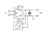
- FIG. 2 is a circuit diagram illustrating a basic configuration of the present invention.
- FIG. 3 is a circuit diagram illustrating a configuration of a high frequency IC according to a first embodiment of the present invention.
- FIG. 4 is a plan view illustrating an example of a transistor element arrangement of a test oscillator and an amplifier according to the first embodiment of the present invention.
- FIG. 5 is a circuit diagram illustrating a configuration of a high frequency IC according to a second embodiment of the present invention.
- FIG. 6 is a circuit diagram illustrating a configuration of a high frequency IC according to a third embodiment of the present invention.
- FIG. 7 is a circuit diagram illustrating a configuration of a high frequency IC according to a fourth embodiment of the present invention.
- FIG. 8 is a circuit diagram illustrating a configuration of a high frequency IC according to a fifth embodiment of the present invention.
- FIG. 9 is a circuit diagram illustrating a configuration of a varactor configuring the high frequency IC according to the fifth embodiment of the present invention.
- FIG. 10 is a circuit diagram illustrating a configuration of a high frequency IC according to a sixth embodiment of the present invention.
- FIG. 11 is a block diagram illustrating a configuration of a high frequency IC according to a seventh embodiment of the present invention.
- FIG. 12 is a block diagram illustrating a configuration of a transmitter IC according to an eighth embodiment of the present invention.
- FIG. 13 is a plan view illustrating a block arrangement on a circuit layout of a transmitter IC according to a ninth embodiment of the present invention.
- FIG. 14 is a block diagram illustrating a configuration of a transmitter IC according to a tenth embodiment of the present invention.
- FIG. 15 is a plan view illustrating a block arrangement on a circuit layout of a transmitter IC according to an eleventh embodiment of the present invention.
- FIG. 16 is a block diagram illustrating a configuration of a transceiver IC according to a twelfth embodiment of the present invention.
- FIG. 17 is a block diagram illustrating a configuration of a millimeter-wave radar module according to a thirteenth embodiment of the present invention.
- the invention will be described in a plurality of embodiments or sections when required as a matter of convenience. However, these sections or embodiments are not irrelevant to each other unless otherwise stated and one relates to a modification, details, supplementary description or the like of the entire or part of the other.
- the number of elements is not limited to a specific number unless otherwise stated or except for the case in which the number is apparently limited to a specific number in principle, and the number larger or smaller than the specified number is also applicable.
- Positions, sizes, shapes, and ranges of individual configurations illustrated in the drawings and the like may not represent actual positions, sizes, shapes, and ranges in order to facilitate understanding of the invention. For this reason, the present invention is not necessarily limited to the positions, the sizes, the shapes, and the ranges disclosed in the drawings and the like.
- a high frequency IC according to a first embodiment will be described on the basis of FIGS. 2 to 4 .
- the high frequency IC is a high frequency IC that includes a differential amplifier 111 having an inductive load 113 and a test oscillator 112 .
- the test oscillator 112 commonly uses the inductive load 113 of the amplifier 111 .
- both ends of the inductive load 113 are connected to an output of the differential amplifier 111 and are connected to an output of the test transmitter 112 .
- the differential amplifier 111 has a bias voltage terminal VBIAS 1 to switch an operation state into an active state/inactive state and the oscillator 112 has a bias voltage terminal VBIAS 2 to switch an operation state into an active state/inactive state.
- VBIAS 1 bias voltage terminal
- VBIAS 2 bias voltage terminal
- the inductive load 113 connected to the differential amplifier 111 is connected to a side opposite to an input of the differential amplifier 111 , as illustrated in FIG. 2 .
- the inductive load 113 can be used for various purposes such as filtering of an output signal, attenuation of noise from a power supply, output impedance matching, provision of impedance in a high band, and improvement of gain.
- the inductive load 113 is also used for an operation of the test transmitter 112 , it is possible to avoid increase in a cost and area of individually providing an inductor for the transmitter.
- the differential amplifier 111 and the test oscillator 112 configuring the high frequency IC according to the first embodiment will be described in detail using FIG. 3 .
- all transistors are configured with bipolar transistors for the sake of convenience; however, the transistors configured with other transistors such as MOSFETs have the same effects.
- the differential amplifier 111 includes transistors 1111 and 1112 and resistive elements 1113 , 1114 , and 1115 .
- a base terminal of the transistor 1111 is connected to an input terminal INP of the high frequency IC and the resistor 1114 and a base terminal of the transistor 1112 is connected to an input terminal INN of the high frequency IC and the resistor 1115 .
- Emitter terminals of the transistors 1112 and 1113 are connected to a GND through the resistor 1113 .
- a collector terminal of the transistor 1111 is connected to a terminal 1131 of an inductor 113 , a capacitor 114 , and an output terminal OUTP and a collector terminal of the transistor 1112 is connected to a terminal 1132 of the inductor 113 , a capacitor 115 , and an output terminal OUTN.
- the bias voltage terminal VBIAS 1 is connected to the base terminals of the transistors 1111 and 1112 through the resistors 1114 and 1115 , in order not to affect a high frequency characteristic.
- the test oscillator 112 includes transistors 1121 and 1122 , capacitors 1124 and 1125 , and resistors 1123 , 1126 , and 1127 .
- a collector terminal of the transistor 1121 is connected to a base terminal of the transistor 1122 through the capacitor 1124 and at the same time a collector terminal of the transistor 1122 is connected to a base terminal of the transistor 1121 through the capacitor 1125 to form a positive feedback loop.
- the collector terminal of the transistor 1121 is connected to the terminal 1131 of the inductor 113 , the capacitor 114 , and the output terminal OUTP and the collector terminal of the transistor 1122 is connected to the terminal 1132 of the inductor 113 , the capacitor 115 , and the output terminal OUTN.
- the emitter terminals of the transistors 1112 and 1113 are connected to the GND through the resistor 1113 .
- the bias voltage terminal VBIAS 1 is connected to the base terminals of the transistors 1111 and 1112 through the resistors 1114 and 1115 , in order not to affect a high frequency characteristic.
- a middle point 1133 of the inductor 113 is connected to a power supply terminal VCC and supplies power to the differential amplifier 111 and the test oscillator 112 .
- FIG. 3 has a configuration in which the collectors of the transistors 111 and 112 configuring the differential amplifier 111 are connected to the terminals of the inductor 113 and an output of the test transmitter 112 is connected between the terminals of the inductor 113 and the collectors of the transistors.
- the high frequency IC has at least two operation modes.
- a first operation mode is a normal operation mode in which a high frequency signal input from the outside of the high frequency IC is amplified and then is output to the outside.
- a second operation mode is a test operation mode in which, at the time of a shipment test of the high frequency IC, a high frequency signal is generated from the test oscillator implemented inside of the high frequency IC according to the present invention, and a signal level and a frequency of the generated signal are confirmed to confirm whether the circuit is normally operated.
- a bias voltage of the bias voltage terminal VBIAS 2 is decreased to a GND level and the test oscillator is turned off. Meanwhile, a direct-current voltage value at which the differential amplifier 112 is normally operated is applied as a bias voltage of the bias voltage terminal VBIAS 1 and the differential amplifier is turned on. As a result, the high frequency IC can amplify the external input signal described above and output the external input signal to the outside.
- the bias voltage of the bias voltage terminal VBIAS 1 is decreased to the GND level and the differential amplifier is turned off. Meanwhile, a direct-current voltage value at which the test oscillator 112 is normally operated is applied as the bias voltage of the bias voltage terminal VBIAS 2 and the test oscillator is turned on. As a result, the test oscillator outputs an oscillation signal at a resonance frequency determined by parasitic capacities such as the inductor 113 , the capacitors 114 and 115 , and the transistors.
- test oscillator 112 is arranged on a rear step of the differential amplifier 111 , it is possible to make use of advantages in terms of power loss and a noise characteristic, as compared with the case in which the test oscillator is arranged on a front step of the differential amplifier 111 .
- FIG. 4 schematically illustrates an arrangement in a chip layout of the transistors 1111 and 1112 configuring the differential amplifier 111 and the transistors 1121 and 1122 configuring the test oscillator 112 in the first embodiment.
- the transistors 1111 and 1112 of the differential amplifier 111 and the transistors 1121 and 1122 of the test oscillator 112 preferably have the same current driving ability.
- the transistors 1111 , 1112 , 1121 , and 1122 are arranged in a common centroidal manner, so that characteristics of the transistors can be almost matched with each other.
- the test oscillator 112 can be arranged on a load side of the differential amplifier 111 .
- the oscillator is arranged on the front step of the differential amplifier, as in PTL 1, loss of power input to the differential amplifier 111 is suppressed, and good noise performance can be secured in the normal operation mode.
- a built-in high frequency signal source for a test is provided to make an externally attached expensive high frequency signal source unnecessary, so that a test cost at the time of an IC shipment can be suppressed.
- the transistors are arranged as illustrated in FIG.
- the high frequency IC can be shipped with the high frequency characteristic of the high frequency IC guaranteed by carrying out only a direct-current operation test while securing good noise performance in the normal operation mode of the transmitter and the receiver, so that the test cost can be reduced.
- a high frequency IC according to a second embodiment will be described on the basis of FIG. 5 .
- the second embodiment is a modification of the high frequency IC according to the first embodiment.
- an inductor 113 is configured using a transformer.
- a primary side of the transformer is connected to a differential amplifier 111 and a test oscillator 112 and a secondary side is connected to output terminals OUTP and OUTN of the high frequency IC. Since the other circuit configuration and circuit operation and a common centroidal arrangement of transistors are the same as those in the first embodiment, repetitive description is omitted.
- a transformer output is taken while securing of good noise performance and reduction of a test cost at the time of an IC shipment are realized in a similar manner to the first embodiment. Therefore, there is an effect of facilitating impedance matching with an amplifier arranged on a rear step.
- a high frequency IC according to a third embodiment will be described on the basis of FIG. 6 .
- the third embodiment is a modification of the high frequency IC according to the first embodiment.
- a differential amplifier 111 is a cascode amplifier.
- a circuit configuration of the differential amplifier 111 will be described.
- the differential amplifier 111 includes transistors 1111 , 1112 , 1116 , and 1117 and resistive elements 1113 , 1114 , and 1115 .
- Abase terminal of the transistor 1111 is connected to an input terminal INP of the high frequency IC and the resistor 1114 and a base terminal of the transistor 1112 is connected to an input terminal INN of the high frequency IC and the resistor 1115 .
- Emitter terminals of the transistors 1112 and 1113 are connected to a GND through the resistor 1113 .
- a collector terminal of the transistor 1111 is connected to an emitter terminal of the transistor 1116 and a collector terminal of the transistor 1112 is connected to an emitter terminal of the transistor 1117 .
- Base terminals of the transistors 1116 and 1117 are connected to a power supply terminal.
- a collector terminal of the transistor 1116 is connected to a terminal 1131 of an inductor 113 , a capacitor 114 , and an output terminal OUTP and a collector terminal of the transistor 1117 is connected to a terminal 1132 of the inductor 113 , a capacitor 115 , and an output terminal OUTN.
- a bias voltage terminal VBIAS 1 is connected to the base terminals of the transistors 1111 and 1112 through the resistors 1114 and 1115 , in order not to affect a high frequency characteristic.
- a test oscillator 112 and the inductor 113 have the same circuit configurations as those in the first embodiment, description thereof is omitted. In addition, since two operation modes and operation principles thereof are also the same, repetitive description is omitted.
- the cascode configuration is adopted while securing of good noise performance and reduction of a test cost at the time of an IC shipment are realized in a similar manner to the first embodiment, so that an isolation characteristic between an input and an output is secured and an influence by a mirror effect can be reduced. Therefore, an operation frequency band can be extended.
- a high frequency IC according to a fourth embodiment will be described on the basis of FIG. 7 .
- the fourth embodiment is a high frequency IC obtained by combining the configuration of the output unit using the transformer 113 illustrated in the second embodiment and the cascode configuration illustrated in the third embodiment. Since a circuit configuration and an operation principle are the same as those in the first to third embodiments, repetitive description is omitted.
- a transformer output is taken while securing of good noise performance and reduction of a test cost at the time of an IC shipment are realized in a similar manner to the first embodiment, so that there is an effect of facilitating impedance matching with an amplifier arranged on a rear step.
- the cascode configuration is adopted, an isolation characteristic between an input and an output is secured and an influence by a mirror effect can be reduced. Therefore, an operation frequency band can be extended.
- a high frequency IC according to a fifth embodiment will be described on the basis of FIG. 8 .
- capacitors 114 and 115 in the high frequency IC according to the fourth embodiment are varactors.
- the varactors 114 and 115 are capacitors in which capacity values can be varied by a control voltage VFINE.
- FIG. 9 is a diagram illustrating a configuration example of the varactor.
- Each of the varactors 114 and 115 includes a capacitor 1141 , a varactor diode, and a resistor 1143 .
- the capacitor 1141 is inserted to separate a direct-current voltage of an anode of the varactor diode from a direct-current voltage of a differential amplifier 111 and a test oscillator, and the resistor 1143 is inserted to fix a potential of the anode of a varactor diode 1142 to a GND potential while separating a high frequency signal.
- an oscillation frequency of the test oscillator in a test operation mode can be varied, a test of frequency dependency of output power of a transmitter chain or the like can be carried out at a low cost, for example in a transmitter IC according to an eighth embodiment to be described below.
- a high frequency IC according to a sixth embodiment will be described on the basis of FIG. 10 .
- a differential amplifier 111 in the high frequency IC according to the fifth embodiment is an emitter degenerative amplifier using an inductor 2117 .
- the differential amplifier 111 includes transistors 1111 , 1112 , 1116 , and 1117 , resistive elements 1113 , 1114 , and 1115 , and inductors 2218 and 2117 .
- a base terminal of the transistor 1111 is connected to an input terminal INP of the high frequency IC and the resistor 1114 and a base terminal of the transistor 1112 is connected to an input terminal INN of the high frequency IC and the resistor 1115 .
- An emitter terminal of the transistor 1112 is connected to a GND through the inductor 2117 and the resistor 1113 and the transistor 1113 is connected to the GND through the inductor 2118 and the resistor 1113 .
- a collector terminal of the transistor 1111 is connected to an emitter terminal of the transistor 1116 and a collector terminal of the transistor 1112 is connected to an emitter terminal of the transistor 1117 .
- Base terminals of the transistors 1116 and 1117 are connected to a power supply terminal.
- a collector terminal of the transistor 1116 is connected to a terminal 1131 of an inductor 113 , a capacitor 114 , and an output terminal OUTP and a collector terminal of the transistor 1117 is connected to a terminal 1132 of the inductor 113 , a capacitor 115 , and an output terminal OUTN.
- a bias voltage terminal VBIAS 1 is connected to the base terminals of the transistors 1111 and 1112 through the resistors 1114 and 1115 , in order not to affect a high frequency characteristic. Meanwhile, since a test oscillator 112 and the inductor 113 have the same circuit configurations as those in the fifth embodiment, description thereof is omitted.
- the inductor is connected to the emitter terminal of the differential amplifier 111 , power matching and noise matching can be achieved at the same time. Therefore, noise performance can be improved as compared with the high frequency ICs according to the first to fifth embodiments.
- this embodiment is used in a receiver IC according to a ninth embodiment to be described below, a particularly high effect is obtained.
- a high frequency IC according to a seventh embodiment will be described on the basis of FIG. 11 .
- a power sensor 140 is included in output terminals OUTP and OUTN in the high frequency IC according to each of the first to sixth embodiments.
- the power sensor 140 is a circuit block that detects a high frequency signal output from a differential amplifier 111 and a test oscillator 112 to output a direct-current voltage or a direct current proportional to an output signal level thereof.
- a test oscillator 112 detects a high frequency signal output from a differential amplifier 111 and a test oscillator 112 to output a direct-current voltage or a direct current proportional to an output signal level thereof.
- the high frequency IC according to the seventh embodiment is a high frequency IC that includes at least the differential amplifier 111 having an inductive load 113 , the test oscillator 112 , and the power sensor 140 , as illustrated in FIG. 11 .
- the test oscillator 112 commonly uses the inductive load 113 of the amplifier 111 , the amplifier 111 has a bias voltage terminal VBIAS 1 to switch an operation state into an active state/inactive state, and the oscillator 112 has a bias voltage terminal VBIAS 2 to switch an operation state into an active state/inactive state.
- the amplifier 111 in a test operation mode, the amplifier 111 is inactivated and the test oscillator 112 is activated and in a normal operation mode, the amplifier 111 is activated and the test oscillator 112 is inactivated.
- the high frequency IC has at least two operation modes.
- a first operation mode is a normal operation mode in which a high frequency signal input from the outside of the high frequency IC is amplified and then is output to the outside.
- a second operation mode is a test operation mode in which, at the time of a shipment test of the high frequency IC, a high frequency signal is generated from the test oscillator implemented inside of the high frequency IC according to this embodiment, the generated high frequency signal is converted into a direct-current voltage or a direct-current voltage according to a signal level of the high frequency signal by the power sensor 140 , and a direct-current voltage value thereof is monitored to confirm whether the circuit is normally operated.
- a bias voltage of the bias voltage terminal VBIAS 2 is decreased to a GND level and the test oscillator is turned off. Meanwhile, a direct-current voltage value at which the differential amplifier 112 is normally operated is applied as a bias voltage of the bias voltage terminal VBIAS 1 and the differential amplifier is turned on. As a result, the high frequency IC can amplify the external input signal described above and output the external input signal to the outside.
- the bias voltage of the bias voltage terminal VBIAS 1 is decreased to the GND level and the differential amplifier is turned off. Meanwhile, a direct-current voltage value at which the test oscillator 112 is normally operated is applied as the bias voltage of the bias voltage terminal VBIAS 2 and the test oscillator is turned on. As a result, the test oscillator 112 outputs an oscillation signal at a resonance frequency determined by parasitic capacities such as the inductor 113 , the capacitors 114 and 115 , and the transistors.
- the high frequency signal generated by the test oscillator 112 is input to the power sensor 140 and is converted into a direct-current voltage or a direct current according to a signal level of the high frequency signal and a direct-current voltage value or a direct current value thereof is monitored.
- the signal level of the high frequency signal generated by the test oscillator 112 can be converted into the direct-current voltage by the power sensor 140 . Therefore, since a high frequency measurer can be removed completely from a test environment, a test cost can be reduced further as compared with the first to sixth embodiments.
- a transmitter IC according to an eighth embodiment will be described on the basis of FIGS. 12 and 13 .
- FIG. 12 is a diagram illustrating a circuit configuration of a transmitter IC 100 according to the eighth embodiment.
- a programmable gain amplifier (PGA) 120 a power amplifier (PA) 130 , and a power sensor 140 are connected to a rear step of the high frequency IC illustrated in each of the first to sixth embodiments.
- the high frequency IC illustrated in each of the first to sixth embodiments serves as a block in an IC, the high frequency IC is defined as a differential amplifier 110 with a test oscillator in this embodiment and the following embodiments.
- the transmitter IC includes at least the differential amplifier 110 with the test oscillator that is illustrated in each of the first to sixth embodiments, the PGA 120 that can control circuit gain arbitrarily, the PA 130 that outputs power to drive a transmission antenna outside the IC, and the power sensor 140 that outputs a direct-current voltage or a direct current proportional to an output signal level of a high frequency output signal of the PA 130 .
- Input terminals INP and INN of the transmitter IC are connected to the differential amplifier 110 with the test oscillator, an output of the differential amplifier 110 with the test oscillator is connected to the PGA 120 , an output of the PGA 120 is connected to the PA 130 , and an output of the PA 130 is connected to the power sensor 140 and output terminals OUTP and OUTN of the transmitter IC.
- the transmitter IC 100 has at least two operation modes in a similar manner to the first to seventh embodiments.
- a first operation mode is a normal operation mode in which a high frequency signal input from the outside of the transmitter IC 100 is amplified and then is output to the outside.
- a second operation mode is a test operation mode in which, at the time of a shipment test of the transmitter IC 100 , a high frequency signal is generated from a test oscillator 112 in the differential amplifier 110 with the test oscillator implemented inside of the transmitter IC 100 according to the present invention, and a signal level and a frequency of the generated signal are confirmed to confirm whether the circuit is normally operated.
- a bias voltage of the bias voltage terminal VBIAS 2 described in the first embodiment is decreased to a GND level and the test oscillator 112 is turned off. Meanwhile, a direct-current voltage value at which the differential amplifier 111 is normally operated is applied as a bias voltage of the bias voltage terminal VBIAS 1 described in the first embodiment and the differential amplifier is turned on.
- the transmitter IC can amplify an external input signal passing through a transmission chain connected to the differential amplifier 111 , the PGA 120 , and the PA 130 and output the external input signal to the outside of the transmitter IC 100 .
- the bias voltage of the bias voltage terminal VBIAS 1 is decreased to the GND level and the differential amplifier 111 is turned off. Meanwhile, a direct-current voltage value at which the test oscillator 112 is normally operated is applied as the bias voltage of the bias voltage terminal VBIAS 2 and the test oscillator is turned on. As a result, the test oscillator 112 outputs an oscillation signal at a resonance frequency determined by parasitic capacities such as an inductor 113 , capacitors 114 and 115 , and transistors.
- the high frequency signal generated by the test oscillator 112 is amplified by the PGA 120 and the PA 130 , is then input to the power sensor 140 , and is converted into a direct-current voltage or a direct current according to a signal level of the high frequency signal and a direct-current voltage value or a direct current value thereof is monitored.
- the differential amplifier 110 with the test oscillator, the PGA 120 , the PA 130 , and the power sensor 140 are configured as one system; however, a plurality of sets of these elements can be included to realize a multi-channel configuration.
- the plurality of sets may be arranged on the same chip or different chips.
- FIG. 13 is a schematic diagram illustrating an arrangement of individual blocks on a chip layout of the transmitter IC 100 according to the eighth embodiment.
- transistors of the differential amplifier 111 and the test oscillator 112 in the differential amplifier 110 with the test oscillator preferably have the same current driving ability in terms of securing precision at the time of the IC shipment test.
- the differential amplifier and the test oscillator are preferably close to each other, as illustrated in FIG. 13 .
- test precision can be further improved.
- the transmitter IC 100 in the transmitter IC 100 , good noise performance can be secured in the normal operation mode and a built-in high frequency signal source for a test is provided to make an externally attached expensive high frequency signal source unnecessary, so that a test cost at the time of an IC shipment can be suppressed.
- a test of frequency dependency of an output voltage output by the transmitter IC 100 is also enabled by swinging the VFINE voltage and a shipment yield of the transmitter IC is improved, so that a cost can be further reduced.
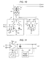
- a receiver IC according to a ninth embodiment will be described on the basis of FIGS. 14 and 15 .
- FIG. 14 is a diagram illustrating a circuit configuration of a receiver IC 200 according to the ninth embodiment.
- the ninth embodiment is the receiver IC 200 in which a mixer (frequency converter) (MIX) 220 and an intermediate frequency amplifier (IFA) 230 are connected to a rear step of the differential amplifier 110 with the test oscillator illustrated in each of the first to sixth embodiments.
- MIX frequency converter
- IFA intermediate frequency amplifier
- the receiver IC includes at least the differential amplifier 110 with the test oscillator illustrated in each of the first to sixth embodiments, the MIX 220 that mixes an output signal of the differential amplifier 110 with the test oscillator and a local signal of a high frequency supplied from the outside of the receiver IC, performs frequency conversion, and generates an intermediate frequency signal, and the IFA 230 that amplifies the intermediate frequency signal generated by the MIX 220 to an appropriate signal level.
- Input terminals INP and INN of the receiver IC 200 are connected to the differential amplifier 110 with the test oscillator, an output of the differential amplifier 110 with the test oscillator and a local signal terminal LO of the receiver IC are connected to the MIX 220 , an output of the MIX 220 is connected to the IFA 230 , and an output of the IFA 230 is connected to output terminals OUTP and OUTN of the receiver IC 200 .
- a first operation mode is a normal operation mode in which a high frequency signal input from the outside of the receiver IC 200 is amplified, the high frequency signal is then down-converted into an intermediate frequency by the MIX 200 , and an intermediate frequency band signal amplified by the IFA 230 is output to the outside.
- a second operation mode is a test operation mode in which, at the time of a shipment test of the receiver IC 200 , a high frequency signal is generated from a test oscillator 112 in the differential amplifier 110 with the test oscillator implemented inside of the receiver IC 200 according to the present invention, and a signal level of an intermediate frequency band signal down-converted into an intermediate frequency band by the MIX 220 is confirmed to confirm whether the circuit is normally operated.
- a bias voltage of the bias voltage terminal VBIAS 2 described in the first embodiment is decreased to a GND level and the test oscillator 112 is turned off. Meanwhile, a direct-current voltage value at which a differential amplifier 111 is normally operated is applied as a bias voltage of the bias voltage terminal VBIAS 1 described in the first embodiment and the differential amplifier is turned on.
- the receiver IC 200 can amplify an external input signal passing through a reception chain connected to the differential amplifier 111 , the MIX 220 , and the IFA 230 and output the external input signal to the outside of the receiver IC 200 .
- the bias voltage of the bias voltage terminal VBIAS 1 is decreased to the GND level and the differential amplifier 111 is turned off. Meanwhile, a direct-current voltage value at which the test oscillator 112 is normally operated is applied as the bias voltage of the bias voltage terminal VBIAS 2 and the test oscillator is turned on. As a result, the test oscillator 112 outputs an oscillation signal at a resonance frequency determined by parasitic capacities such as an inductor 113 , capacitors 114 and 115 , and transistors.
- the high frequency signal generated by the test oscillator 112 is down-converted into an intermediate frequency band signal by the MIX 220 and is amplified by the IFA 230 and then a signal level of the intermediate frequency band signal in the output terminals OUTP and OUTN of the receiver IC 200 is monitored. Since a frequency of the above-described intermediate frequency band signal is sufficiently low as compared with a frequency of the high frequency signal generated by the above-described test oscillator 112 , a signal level thereof can be measured without requiring an expensive measurer.
- the differential amplifier 110 with the test oscillator, the MIX 220 , and the IFA 230 are configured as one system; however, a plurality of sets of these elements can be included to realize a multi-channel configuration.
- the plurality of sets may be arranged on the same chip or different chips.
- FIG. 15 is a schematic diagram illustrating an arrangement of individual blocks on a chip layout of the receiver IC 200 according to the ninth embodiment.
- transistors of the differential amplifier 111 and the test oscillator 112 in the differential amplifier 110 with the test oscillator preferably have the same current driving ability in terms of securing precision at the time of the IC shipment test.
- the differential amplifier 111 and the test oscillator 112 are preferably close to each other, as illustrated in FIG. 15 .
- test precision can be further improved.
- the receiver IC 200 in the receiver IC 200 , good noise performance can be secured in the normal operation mode and a built-in high frequency signal source for a test is provided to make an externally attached expensive high frequency signal source unnecessary, so that a test cost at the time of an IC shipment can be suppressed.
- noise performance can be improved as compared with the differential amplifier 110 with the test oscillator illustrated in each of the first to fifth embodiments.
- a transceiver IC according to a tenth embodiment will be described on the basis of FIG. 16 .
- a transceiver IC 10 includes a transmission block 100 , a reception block 200 , and a SYNTH 310 .
- the reception block 200 includes at least the differential amplifier 110 with the test oscillator illustrated in each of the first to sixth embodiments, a MIX 220 that mixes an output signal of the differential amplifier 110 with the test oscillator and a local signal of a high frequency supplied from the SYNTH 310 in the transceiver IC 300 , performs frequency conversion, and generates an intermediate frequency signal, and an IFA 230 that amplifies the intermediate frequency signal generated by the MIX 220 to an appropriate signal level.
- the transmission block 100 includes an input differential amplifier 150 , a PGA 120 that can control circuit gain arbitrarily, a PA 130 that outputs power to drive a transmission antenna outside the IC, and a power sensor 140 that outputs a direct-current voltage or a direct current proportional to an output signal level of a high frequency output signal of the PA 120 .
- the SYNTH 310 (frequency synthesizer) supplies a high frequency signal to the transmission block and the MIX 220 in the reception block in a normal operation mode.
- An output of the SYNTH 310 in the transceiver IC 10 is connected to the input differential amplifier 150 of the transmission block 100 and the MIX 220 of the reception block.
- an output of the input differential amplifier 150 is connected to the PGA 120
- an output of the PGA 120 is connected to the PA 130
- an output of the PA 130 is connected to the power sensor 140 and transmission output terminals TXOUTP and TXOUTN of the transceiver IC 10 .
- input terminals RXINP and RXINN of the transceiver IC 10 are connected to the differential amplifier 110 with the test oscillator, an output of the differential amplifier 110 with the test oscillator and a local signal of the SYNTH 310 are connected to the MIX 220 , an output of the MIX 220 is connected to the IFA 230 , and an output of the IFA 230 is connected to output terminals IFOUTP and IFOUTN of the transceiver IC 10 .
- a first operation mode is a normal operation mode in which, in the transmission block 100 , a high frequency signal generated from the SYNTH 310 is amplified and then is output to the outside and in the reception block 200 , a high frequency signal input from the outside of the transceiver IC 10 is amplified, the high frequency signal is then down-converted into an intermediate frequency by the MIX 220 , and an intermediate frequency band signal amplified by the IFA 230 is output to the outside.
- a second operation mode is a test operation mode in which, at the time of a shipment test of the transceiver IC 10 , in the transmission block 100 , a high frequency signal generated from the SYNTH 310 is amplified by a transmission chain, and a signal level of the amplified high frequency signal is confirmed to confirm whether the circuit is normally operated and in the reception block, a high frequency signal is generated from a test oscillator 112 in the differential amplifier 110 with the test oscillator implemented inside of the transceiver IC 10 , and a signal level of an intermediate frequency band signal down-converted into an intermediate frequency band by the MIX 220 is confirmed to confirm whether the circuit is normally operated.
- the high frequency signal supplied by the SYNTH 310 passes through a transmission chain connected to the input differential amplifier 150 , the PGA 120 , and the PA 130 , so that the high frequency signal is amplified, and the high frequency signal is output to the outside of the transceiver IC 10 .
- a bias voltage of the bias voltage terminal VBIAS 2 described in the first embodiment is decreased to a GND level and the test oscillator 112 is turned off. Meanwhile, a direct-current voltage value at which a differential amplifier 111 is normally operated is applied as a bias voltage of the bias voltage terminal VBIAS 1 also described in the first embodiment and the differential amplifier is turned on.
- the transceiver IC 10 can amplify an external input signal passing through a reception chain connected to the differential amplifier 111 , the MIX 220 , and the IFA 230 and output the external input signal to the outside of the transceiver IC 10 .
- the high frequency signal supplied by the SYNTH 310 is amplified by the input differential amplifier 150 , the PGA 120 , and the PA 130 , is then input to the power sensor 140 , and is converted into a direct-current voltage or a direct current according to a signal level of the high frequency signal and a direct-current voltage value or a direct current value thereof is monitored.
- the bias voltage of the bias voltage terminal VBIAS 1 is decreased to the GND level and the differential amplifier 111 is turned off.
- a direct-current voltage value at which the test oscillator 112 is normally operated is applied as the bias voltage of the bias voltage terminal VBIAS 2 and the test oscillator is turned on.
- the test oscillator 112 outputs an oscillation signal at a resonance frequency determined by parasitic capacities such as an inductor 113 , capacitors 114 and 115 , and transistors.
- the high frequency signal generated by the test oscillator 112 is down-converted into an intermediate frequency band signal by the MIX 220 and is amplified by the IFA 230 and then a signal level of the intermediate frequency band signal in the output terminals OUTP and OUTN of the transceiver IC 10 is monitored. Since a frequency of the above-described intermediate frequency band signal is sufficiently low as compared with a frequency of the high frequency signal generated by the above-described test oscillator 112 , a signal level thereof can be measured without requiring an expensive measurer.
- the transceiver IC 10 in the transceiver IC 10 , good noise performance can be secured in the normal operation mode and a built-in high frequency signal source for a test is provided to make an externally attached expensive high frequency signal source unnecessary, so that a test cost at the time of an IC shipment can be suppressed.
- noise performance can be improved as compared with the differential amplifier 110 with the test oscillator illustrated in each of the first to fifth embodiments.
- a millimeter-wave radar module according to an eleventh embodiment will be described on the basis of FIG. 17 .
- a millimeter-wave radar module 1 includes at least any one of the high frequency IC 110 , the transmitter IC 100 , the receiver IC 200 , and the transceiver IC 10 illustrated in the first to tenth embodiments, a BBIC 400 , a transmission antenna TXANT 500 , and a reception antenna RXANT 600 .
- the millimeter-wave radar module 1 including the transceiver IC 10 , the BBIC 400 , the transmission antenna TXANT 500 , and the reception antenna RXANT 600 will be described.
- the millimeter-wave radar module 1 controls a modulation operation of a high frequency signal output from a SYNTH 310 in the transceiver IC 10 by a control signal from the BBIC 400 .
- An output of the SYNTH 310 is connected to a transmission block 100 , the transmission block 100 performs power amplification of an input high frequency signal and is connected to the transmission antenna 500 , and the transmission antenna 500 emits the input high frequency signal to space.
- the high frequency signal received by the reception antenna 600 is input to the reception block 200 in the transceiver IC 10 and the reception block 200 performs amplification and down-conversion of the received high frequency signal and outputs a down-converted intermediate frequency band signal to the BBIC 400 .
- signal processing of the input intermediate frequency band signal is performed and detection of a target is performed.
- the millimeter-wave radar module 1 can be realized using the high frequency IC 110 , the transmitter IC 100 , the receiver IC 200 , and the transceiver IC 10 of a low cost illustrated in the first to tenth embodiments, a cost of the millimeter-wave radar module can be reduced.
- the present invention is not limited to the embodiments described above and various modifications are included.
- a part of a configuration of a certain embodiment can be replaced by a configuration of another embodiment and the configuration of another embodiment can also be added to the configuration of the certain embodiment.
- addition, deletion, and replacement of the configuration of another embodiment are possible.
Landscapes
- Amplifiers (AREA)
- Inductance-Capacitance Distribution Constants And Capacitance-Resistance Oscillators (AREA)
Abstract
Description
- PTL 1: JP-2011-205280 A
- NPL 1: supervision of translation by Kuroda (2002) “RF microelectronics” published by Maruzen, pp. 47-52
Claims (14)
Applications Claiming Priority (2)
| Application Number | Priority Date | Filing Date | Title |
|---|---|---|---|
| JP2014181453A JP6476669B2 (en) | 2014-09-05 | 2014-09-05 | High frequency IC and wireless communication module |
| JP2014-181453 | 2014-09-05 |
Publications (2)
| Publication Number | Publication Date |
|---|---|
| US20160072434A1 US20160072434A1 (en) | 2016-03-10 |
| US9444402B2 true US9444402B2 (en) | 2016-09-13 |
Family
ID=55438456
Family Applications (1)
| Application Number | Title | Priority Date | Filing Date |
|---|---|---|---|
| US14/846,601 Expired - Fee Related US9444402B2 (en) | 2014-09-05 | 2015-09-04 | High frequency integrated circuit and device using same |
Country Status (2)
| Country | Link |
|---|---|
| US (1) | US9444402B2 (en) |
| JP (1) | JP6476669B2 (en) |
Families Citing this family (4)
| Publication number | Priority date | Publication date | Assignee | Title |
|---|---|---|---|---|
| DK3531073T3 (en) * | 2014-07-18 | 2020-11-30 | Apator Miitors Aps | METHOD AND SYSTEM FOR TESTING AND CALIBRATION OF WIRELESS CONSUMER METERS |
| NL2015303B1 (en) * | 2015-08-13 | 2017-02-28 | Prodrive Tech Bv | Electric power converter and MRI system comprising such converter. |
| JP2017200173A (en) * | 2016-04-22 | 2017-11-02 | パナソニックIpマネジメント株式会社 | Differential amplifier circuit and radar device |
| FR3055173B1 (en) * | 2016-08-22 | 2019-08-16 | Devialet | AMPLIFIER DEVICE COMPRISING A COMPENSATION CIRCUIT |
Citations (2)
| Publication number | Priority date | Publication date | Assignee | Title |
|---|---|---|---|---|
| US20110234204A1 (en) | 2010-03-25 | 2011-09-29 | Fujitsu Limited | Radio-frequency power amplifier |
| US20140368285A1 (en) * | 2013-06-14 | 2014-12-18 | Taiwan Semiconductor Manufacturing Co., Ltd. | Voltage-controlled oscillator |
Family Cites Families (11)
| Publication number | Priority date | Publication date | Assignee | Title |
|---|---|---|---|---|
| JP3859924B2 (en) * | 1999-12-28 | 2006-12-20 | シャープ株式会社 | Oscillator circuit |
| JP2004242071A (en) * | 2003-02-06 | 2004-08-26 | Toyota Industries Corp | Semiconductor integrated circuit |
| JP4536528B2 (en) * | 2004-01-23 | 2010-09-01 | パナソニック株式会社 | Low noise bias circuit for differential and differential signal processing device |
| JPWO2006109731A1 (en) * | 2005-04-08 | 2008-11-20 | 松下電器産業株式会社 | High frequency amplifier and transmission / reception system |
| JP2011097638A (en) * | 2006-02-27 | 2011-05-12 | Mitsubishi Electric Corp | Variable gain amplifier |
| US7336138B2 (en) * | 2006-04-28 | 2008-02-26 | Renesas Technology Corp. | Embedded structure circuit for VCO and regulator |
| JP2009152704A (en) * | 2007-12-19 | 2009-07-09 | Sharp Corp | Oscillation circuit, abnormal oscillation inspection method, high-frequency receiver, and high-frequency transmitter |
| JP2009284329A (en) * | 2008-05-23 | 2009-12-03 | Toshiba Corp | Semiconductor integrated circuit device |
| JP5163577B2 (en) * | 2009-03-27 | 2013-03-13 | 富士通株式会社 | Amplifier circuit and transceiver |
| JP5499794B2 (en) * | 2010-03-15 | 2014-05-21 | 富士通株式会社 | Power amplifier |
| CN103023837B (en) * | 2012-12-04 | 2015-09-02 | 开曼群岛威睿电通股份有限公司 | Frequency detection circuit, radio frequency signal processing equipment and inductance capacitance bearing calibration |
-
2014
- 2014-09-05 JP JP2014181453A patent/JP6476669B2/en not_active Expired - Fee Related
-
2015
- 2015-09-04 US US14/846,601 patent/US9444402B2/en not_active Expired - Fee Related
Patent Citations (3)
| Publication number | Priority date | Publication date | Assignee | Title |
|---|---|---|---|---|
| US20110234204A1 (en) | 2010-03-25 | 2011-09-29 | Fujitsu Limited | Radio-frequency power amplifier |
| JP2011205280A (en) | 2010-03-25 | 2011-10-13 | Fujitsu Ltd | Radio-frequency power amplifier |
| US20140368285A1 (en) * | 2013-06-14 | 2014-12-18 | Taiwan Semiconductor Manufacturing Co., Ltd. | Voltage-controlled oscillator |
Non-Patent Citations (1)
| Title |
|---|
| Supervision of translation by Kuroda (2002) "RF microelectronics" published by Maruzen, pp. 47-52. |
Also Published As
| Publication number | Publication date |
|---|---|
| JP6476669B2 (en) | 2019-03-06 |
| JP2016058788A (en) | 2016-04-21 |
| US20160072434A1 (en) | 2016-03-10 |
Similar Documents
| Publication | Publication Date | Title |
|---|---|---|
| JP4768859B2 (en) | SPS receiver with adjustable linearity | |
| US10365308B2 (en) | Wide dynamic range broadband current mode linear detector circuits for high power radio frequency power amplifier | |
| US9444402B2 (en) | High frequency integrated circuit and device using same | |
| US20100273535A1 (en) | Radio-frequency power amplifier device and wireless communication device including the same | |
| US9941923B2 (en) | Radio transceiver circuit | |
| US9209769B2 (en) | Power amplifier and communication device | |
| CN112073010A (en) | Coupling a bias circuit to an amplifier using an adaptive coupling device | |
| KR20180115219A (en) | Power amplifier module and radio frequency module | |
| KR101774143B1 (en) | Unpowered switching module | |
| US20190222238A1 (en) | Radio frequency front-end transmission method and transmission module, chip, and communications terminal | |
| CN103856234A (en) | Concurrent multiband transceiver | |
| US11799511B2 (en) | Transceiver having radio-frequency front-end circuit, dedicated radio-frequency front-end circuit, and switchable matching circuit integrated in same chip | |
| US20160336907A1 (en) | High gain rf power amplifier with negative capacitor | |
| US20150249433A1 (en) | Power amplifier module | |
| TW201404032A (en) | Low noise amplifiers for multiple radio standards | |
| CN114301399B (en) | Bias arrangement of linearized transistors that sense RF signals and provide bias signals at different terminals | |
| US20180159482A1 (en) | Radio frequency module and communication device | |
| US20230170861A1 (en) | Integrated directional coupler for broadband amplifier | |
| US20240305250A1 (en) | Radio-frequency Amplifier with Large Signal Protection | |
| US12250029B2 (en) | System and method for radio frequency (RF) sensing to determine device parameters | |
| Liu et al. | A 28-GHz transceiver front-end with T/R switching achieving 11.2-dBm OP 1dB, 33.8% PAE max and 4-dB NF in 22-nm FD-SOI for 5G communication | |
| US20250096840A1 (en) | Radio-frequency Power Detector with Common Mode Leakage Cancellation | |
| US20250096753A1 (en) | Antenna voltage standing wave ratio (vswr)-tolerant transmission power amplifier | |
| JP2015146537A (en) | Transmitter circuit for millimeter wave transmitter | |
| US12407307B2 (en) | Power amplification circuit, radio-frequency circuit, and communication device |
Legal Events
| Date | Code | Title | Description |
|---|---|---|---|
| AS | Assignment |
Owner name: HITACHI, LTD., JAPAN Free format text: ASSIGNMENT OF ASSIGNORS INTEREST;ASSIGNORS:WACHI, YUSUKE;SOMADA, ICHIRO;OKAZAKI, TAKAO;SIGNING DATES FROM 20150622 TO 20150626;REEL/FRAME:036548/0539 |
|
| ZAAA | Notice of allowance and fees due |
Free format text: ORIGINAL CODE: NOA |
|
| ZAAB | Notice of allowance mailed |
Free format text: ORIGINAL CODE: MN/=. |
|
| STCF | Information on status: patent grant |
Free format text: PATENTED CASE |
|
| AS | Assignment |
Owner name: DENSO CORPORATION, JAPAN Free format text: ASSIGNMENT OF ASSIGNORS INTEREST;ASSIGNOR:HITACHI, LTD.;REEL/FRAME:044412/0701 Effective date: 20171207 |
|
| MAFP | Maintenance fee payment |
Free format text: PAYMENT OF MAINTENANCE FEE, 4TH YEAR, LARGE ENTITY (ORIGINAL EVENT CODE: M1551); ENTITY STATUS OF PATENT OWNER: LARGE ENTITY Year of fee payment: 4 |
|
| FEPP | Fee payment procedure |
Free format text: MAINTENANCE FEE REMINDER MAILED (ORIGINAL EVENT CODE: REM.); ENTITY STATUS OF PATENT OWNER: LARGE ENTITY |
|
| LAPS | Lapse for failure to pay maintenance fees |
Free format text: PATENT EXPIRED FOR FAILURE TO PAY MAINTENANCE FEES (ORIGINAL EVENT CODE: EXP.); ENTITY STATUS OF PATENT OWNER: LARGE ENTITY |
|
| STCH | Information on status: patent discontinuation |
Free format text: PATENT EXPIRED DUE TO NONPAYMENT OF MAINTENANCE FEES UNDER 37 CFR 1.362 |
|
| FP | Lapsed due to failure to pay maintenance fee |
Effective date: 20240913 |