US9438287B2 - Apparatus and method for mitigating loss of signal content - Google Patents
Apparatus and method for mitigating loss of signal content Download PDFInfo
- Publication number
- US9438287B2 US9438287B2 US14/562,499 US201414562499A US9438287B2 US 9438287 B2 US9438287 B2 US 9438287B2 US 201414562499 A US201414562499 A US 201414562499A US 9438287 B2 US9438287 B2 US 9438287B2
- Authority
- US
- United States
- Prior art keywords
- signal
- frequency band
- memory
- channel
- notch
- Prior art date
- Legal status (The legal status is an assumption and is not a legal conclusion. Google has not performed a legal analysis and makes no representation as to the accuracy of the status listed.)
- Active
Links
- 238000000034 method Methods 0.000 title claims abstract description 26
- 230000000116 mitigating effect Effects 0.000 title description 17
- 230000004044 response Effects 0.000 claims abstract description 48
- 230000005540 biological transmission Effects 0.000 claims abstract description 10
- 238000005516 engineering process Methods 0.000 claims description 10
- 238000012546 transfer Methods 0.000 claims description 8
- 239000002070 nanowire Substances 0.000 claims description 7
- 230000015556 catabolic process Effects 0.000 claims description 6
- 238000006731 degradation reaction Methods 0.000 claims description 6
- 230000008859 change Effects 0.000 claims description 5
- 238000004891 communication Methods 0.000 claims description 5
- 230000000694 effects Effects 0.000 description 25
- 230000006870 function Effects 0.000 description 24
- 230000002093 peripheral effect Effects 0.000 description 9
- 230000008569 process Effects 0.000 description 9
- 238000005070 sampling Methods 0.000 description 7
- 230000001413 cellular effect Effects 0.000 description 5
- 238000012545 processing Methods 0.000 description 5
- 238000000354 decomposition reaction Methods 0.000 description 4
- 238000010586 diagram Methods 0.000 description 4
- 230000001747 exhibiting effect Effects 0.000 description 4
- 238000001914 filtration Methods 0.000 description 4
- 238000004458 analytical method Methods 0.000 description 3
- 238000003032 molecular docking Methods 0.000 description 3
- 230000002238 attenuated effect Effects 0.000 description 2
- 230000007613 environmental effect Effects 0.000 description 2
- 230000003993 interaction Effects 0.000 description 2
- 238000012986 modification Methods 0.000 description 2
- 230000004048 modification Effects 0.000 description 2
- 230000003287 optical effect Effects 0.000 description 2
- 239000007787 solid Substances 0.000 description 2
- 238000013519 translation Methods 0.000 description 2
- 238000003491 array Methods 0.000 description 1
- 239000000872 buffer Substances 0.000 description 1
- 239000000969 carrier Substances 0.000 description 1
- 238000012512 characterization method Methods 0.000 description 1
- 238000004590 computer program Methods 0.000 description 1
- 239000000470 constituent Substances 0.000 description 1
- 230000008878 coupling Effects 0.000 description 1
- 238000010168 coupling process Methods 0.000 description 1
- 238000005859 coupling reaction Methods 0.000 description 1
- 230000001419 dependent effect Effects 0.000 description 1
- 238000013461 design Methods 0.000 description 1
- 238000001514 detection method Methods 0.000 description 1
- 230000007774 longterm Effects 0.000 description 1
- 238000010295 mobile communication Methods 0.000 description 1
- 238000012805 post-processing Methods 0.000 description 1
- 238000007781 pre-processing Methods 0.000 description 1
- 238000003672 processing method Methods 0.000 description 1
- 230000002040 relaxant effect Effects 0.000 description 1
- 230000001629 suppression Effects 0.000 description 1
- 208000011580 syndromic disease Diseases 0.000 description 1
- 230000000007 visual effect Effects 0.000 description 1
Images


Classifications
-
- H—ELECTRICITY
- H04—ELECTRIC COMMUNICATION TECHNIQUE
- H04B—TRANSMISSION
- H04B1/00—Details of transmission systems, not covered by a single one of groups H04B3/00 - H04B13/00; Details of transmission systems not characterised by the medium used for transmission
- H04B1/06—Receivers
- H04B1/10—Means associated with receiver for limiting or suppressing noise or interference
- H04B1/1027—Means associated with receiver for limiting or suppressing noise or interference assessing signal quality or detecting noise/interference for the received signal
- H04B1/1036—Means associated with receiver for limiting or suppressing noise or interference assessing signal quality or detecting noise/interference for the received signal with automatic suppression of narrow band noise or interference, e.g. by using tuneable notch filters
-
- H—ELECTRICITY
- H04—ELECTRIC COMMUNICATION TECHNIQUE
- H04B—TRANSMISSION
- H04B1/00—Details of transmission systems, not covered by a single one of groups H04B3/00 - H04B13/00; Details of transmission systems not characterised by the medium used for transmission
- H04B1/02—Transmitters
- H04B1/04—Circuits
- H04B1/0475—Circuits with means for limiting noise, interference or distortion
-
- H—ELECTRICITY
- H04—ELECTRIC COMMUNICATION TECHNIQUE
- H04B—TRANSMISSION
- H04B1/00—Details of transmission systems, not covered by a single one of groups H04B3/00 - H04B13/00; Details of transmission systems not characterised by the medium used for transmission
- H04B1/06—Receivers
- H04B1/10—Means associated with receiver for limiting or suppressing noise or interference
- H04B1/1027—Means associated with receiver for limiting or suppressing noise or interference assessing signal quality or detecting noise/interference for the received signal
- H04B2001/1063—Means associated with receiver for limiting or suppressing noise or interference assessing signal quality or detecting noise/interference for the received signal using a notch filter
-
- H—ELECTRICITY
- H04—ELECTRIC COMMUNICATION TECHNIQUE
- H04L—TRANSMISSION OF DIGITAL INFORMATION, e.g. TELEGRAPHIC COMMUNICATION
- H04L25/00—Baseband systems
- H04L25/02—Details ; arrangements for supplying electrical power along data transmission lines
- H04L25/08—Modifications for reducing interference; Modifications for reducing effects due to line faults ; Receiver end arrangements for detecting or overcoming line faults
- H04L25/085—Arrangements for reducing interference in line transmission systems, e.g. by differential transmission
Definitions
- the lost signal contents which are typically transmitted/received at the higher frequency of the channel frequency response, are identified by a region in which the frequency amplitude is about zero or is heavily attenuated. This region of the frequency response is typically referred to as a “notch” or “notch region”. This notch may also result in inter symbol interference (ISI) in the signal.
- ISI inter symbol interference
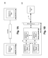
- FIG. 1A illustrates a system having a channel exhibiting a notch in its frequency response, and apparatus for mitigating the notch effect, according to some embodiments of the disclosure.
- FIG. 1B illustrates a system with a solid state drive (SSD) having an apparatus for mitigating a notch effect in a channel between a memory die and a memory controller, according to some embodiments of the disclosure.
- SSD solid state drive
- FIG. 2 illustrates a frequency response of a channel exhibiting a notch.
- FIG. 3 illustrates a frequency response of a channel assuming no notch, and decomposition of part of the frequency response to mitigate the notch effect, according to some embodiments of the disclosure.
- FIG. 4 illustrates a frequency response after oversampling of a signal for transmission and after modulating frequency content in the notch region to a higher frequency band, according to some embodiments of the disclosure.
- FIG. 5 illustrates an apparatus for mitigating the notch effect at the transmitter end, according to some embodiments of the disclosure.
- FIG. 6A illustrates a filter bank of the apparatus for decomposing part of the frequency response into sub-bands to mitigate the notch effect, according to some embodiments of the disclosure.
- FIG. 6B illustrates a waveform showing operation of the filter bank of the apparatus, according to some embodiments of the disclosure.
- FIG. 7 illustrates a frequency response of the channel at the receiver end, according to some embodiments of the disclosure.
- FIG. 8 illustrates a frequency response of the channel at the receiver end, according to some embodiments of the disclosure.
- FIG. 9 illustrates an apparatus for mitigating the notch effect at the receiver end, according to some embodiments of the disclosure.
- FIG. 10 illustrates a flowchart of a method for mitigating the notch effect at the transmitter end, according to some embodiments of the disclosure.
- FIG. 11 illustrates a flowchart of a method for mitigating the notch effect at the receiver end, according to some embodiments of the disclosure.
- FIG. 12 illustrates a smart device or a computer system or a SoC (System-on-Chip) with apparatus for mitigating the notch effect, according to some embodiments.
- SoC System-on-Chip
- signal processing methods are employed to ensure fidelity of a signal transmitted/received at a high input/output transfer rate over a channel (or bus) between two integrated circuits after loss of a portion of the signal contents represented by a notch (a region in which the frequency amplitude is about zero or is heavily attenuated) in the frequency response for the channel.
- filter banks are used to ensure that the contents of the signal (which is oversampled) in a region of the channel notch are recoverable at the receiver.
- pre-processing of the signal prior to transmitting over the channel is performed to move the signal contents, which would have been in the notch region, to a higher frequency band in the frequency response.
- post-processing of the received signal contents is performed by filtering the higher frequency band content and modulating it to a lower frequency band (i.e., the frequency band of the notch region).
- the received content that underwent the channel notch effect
- the modulated signal is then combined with the modulated signal to generate a recovered signal.
- the recovered signal is then down sampled to a frequency of the original signal (i.e., the frequency before that signal was oversampled at the transmitter end).
- signals are represented with lines. Some lines may be thicker, to indicate more constituent signal paths, and/or have arrows at one or more ends, to indicate primary information flow direction. Such indications are not intended to be limiting. Rather, the lines are used in connection with one or more exemplary embodiments to facilitate easier understanding of a circuit or a logical unit. Any represented signal, as dictated by design needs or preferences, may actually comprise one or more signals that may travel in either direction and may be implemented with any suitable type of signal scheme.
- connection means a direct electrical or wireless connection between the things that are connected, without any intermediary devices.
- coupled means either a direct electrical or wireless connection between the things that are connected or an indirect connection through one or more passive or active intermediary devices.
- circuit means one or more passive and/or active components that are arranged to cooperate with one another to provide a desired function.
- signal means at least one current signal, voltage signal or data/clock signal.
- FIG. 1A illustrates system 100 having a channel exhibiting a notch in its frequency response, and apparatus for mitigating the notch effect, according to some embodiments of the disclosure.
- system 100 includes integrated circuits (ICs) 101 and 102 coupled together via channel 103 .
- Channel 103 exhibits a notch in frequency domain.
- notch here generally refers to a characteristic of a channel having a region in the frequency domain where signal content is lost.
- the frequency location or region of the notch in the frequency domain for a channel may be known in advance as part of the channel characterization.
- each IC comprises apparatus 101 a and 102 a to mitigate the notch effect, respectively, so that the signal transmitted by a transmitter is recovered at the receiver with full fidelity. If a signal which is critically sampled is transmitted over a channel that has a frequency response which is not zero at any frequency, then an inverse filtering operation (or an ISI cancellation process) can be used to recover the signal at the receiver. But if the channel has a notch in the frequency domain which leads to virtual loss of the transmitted signal, without something more, that signal cannot be recovered with full fidelity.
- the signal transmitted over the channel is pre-processed by apparatus 101 a (assuming here, that IC 101 is transmitting a signal to IC 102 over channel 103 ) and then post-processed by apparatus 101 b (i.e., the receiver end) so that the effect of the notch is mitigated.
- apparatus 101 a has logic (e.g., samplers, filters, adders, modulators, etc.) that oversamples a signal (which is to be transmitted) so that a high frequency band is available.
- the signal is a critically sampled signal.
- the high frequency band is used to carry the signal content that would have been otherwise suppressed or lost as represented by the notch region in the frequency domain in channel 103 .
- apparatus 101 a comprises a modulator that translates the oversampled signal in the notch region to the newly made available higher frequency band. A driver or transmitter then transmits the oversampled signal along with the oversampled signal in the notch region (which is now translated to a higher frequency band) to IC 102 over channel 103 .
- Channel 103 introduces a notch in a pre-known notch region of the channel and so the oversampled signal in the pre-known notch region is suppressed when the receiver receives the oversampled signal via channel 103 .
- the oversampled signal in the notch region which is translated to the higher frequency band, is also received by the receiver in IC 102 . Since the higher frequency band is away from the frequency band of the notch region, the signal content translated over to the higher frequency band retains fidelity.
- apparatus 102 b post processes the oversampled signal in the notch region (which is translated to the higher frequency band), and the oversampled signal to reconstruct the signal of original frequency (i.e., the signal which was oversampled at the transmitter end).
- apparatus 102 b has similar circuits/logic as apparatus 102 a but in reverse order to reconstruct the signal which was pre-processed by apparatus 102 a.
- FIG. 1B illustrates system 120 with a Solid State Drive (SSD) having an apparatus for mitigating a notch in a channel between a memory die and a memory controller, according to some embodiments of the disclosure. It is pointed out that those elements of FIG. 1B having the same reference numbers (or names) as the elements of any other figure can operate or function in any manner similar to that described, but are not limited to such.
- SSD Solid State Drive
- system 120 comprises SSD 121 and Processor 122 .
- SSD 121 includes an Input/Output (I/O) interface 123 , Memory Controller 124 , and a plurality of memory dies (i.e., Memory Die 1 through Memory Die N, where N is an integer).
- I/O interface 123 is a Serial Advanced Technology Attachment (SATA) interface and interconnect 126 is a SATA compliant bus coupling SSD 121 to Processor 122 .
- SATA Serial Advanced Technology Attachment
- interconnect 126 is a SATA compliant bus coupling SSD 121 to Processor 122 .
- other types of I/O interfaces may be used for I/O interface 123 .
- Serial Attached Small Computer System Interface (SCSI) (or simply SAS) may be used for I/O interface 123 , and interconnect 126 is a SAS compliant interface; Peripheral Component Interconnect Express (PCIe) may also be used for I/O interface 123 as described by PCIe Base 3.0 Specification.
- SCSI Serial Attached Small Computer System Interface
- PCIe Peripheral Component Interconnect Express
- Processor 122 is a microprocessor (such as those designed by Intel Corporation of Santa Clara, Calif.), Digital Signal Processors (DSPs), Field-Programmable Gate Arrays (FPGAs), Application Specific Integrated Circuits (ASICs), or Radio-Frequency Integrated Circuits (RFICs), etc. So as not to obscure the embodiments, a simplified version of SSD 121 is shown. A person skilled in the art would appreciate that there are other logic and circuits needed for complete operation of SSD 121 . For example, encoders, decoders, syndrome calculators, queues, input-output buffers, etc., are not shown.
- SSD 121 and Processor 122 can be packaged together as a single unit.
- SSD 121 and Processor 122 are implemented using a three dimensional integrated circuit (3D IC) technology where various dies are stacked on each other.
- 3D IC three dimensional integrated circuit
- various dies or components of SSD 121 may be implemented as dies that are stacked on a die of Processor 122 to form a stacked die or 3D IC.
- memory dies i.e., Memory Die 1 to Memory Die N, where ‘N’ is an integer
- the memory dies may be distributed in SSD 121 .
- each memory die is a non-volatile memory.
- each memory die is one or more of a single or multi-threshold level NAND flash memory, NOR flash memory, single or multi-level Phase Change Memory (PCM), a three dimensional cross point memory, a resistive memory, nanowire memory, ferro-electric transistor random access memory (FeTRAM), magnetoresistive random access memory (MRAM) memory that incorporates memristor technology, or spin transfer torque (STT)-MRAM, or a combination of any of the above, etc.
- PCM Phase Change Memory
- MRAM magnetoresistive random access memory
- Memory Controller 124 includes apparatus 101 b - 1 through 101 b -N (where, N is an integer) to pre-process the signal transmitted over channel 125 to memory dies.
- channel 125 is an Open NAND Flash Interface (ONFI) specification compliant interface (e.g., ONFI-4 (4.0 revision released Apr. 2, 2014)).
- ONFI-4 4.0 revision released Apr. 2, 2014
- An ONFI-4 channel supports data transfer at 800 Mega Transfers per second (MT/s).
- MT/s Mega Transfers per second
- other types of interfaces may be used for communicating between Memory Controller 124 and Memory Dies.
- each memory die includes apparatus 101 a - 1 through 101 a -N to post-process the received signal and to mitigate the notch effect manifested by channel 125 . While the embodiments are described with reference to Memory Controller 124 transmitting to Memory Dies 1 through N, for example, both transmit and receive logic/circuits are included in both Memory Controller 124 and the memory dies.
- Each of apparatus 101 a - 1 through 101 a -N performs the same function as apparatus 101 a
- each of apparatus 101 b - 1 through 101 b -N performs the same function as apparatus 102 a when Memory Controller 124 is the transmitting end and Memory Die is the receiving end.
- the embodiments are not limited to an SSD, and can be applied to any communication system that uses a channel having a notch.
- FIG. 2 illustrates frequency response 200 of a channel (e.g., 103 / 125 ) exhibiting a notch effect. It is pointed out that those elements of FIG. 2 having the same reference numbers (or names) as the elements of any other figure can operate or function in any manner similar to that described, but are not limited to such.
- x-axis is normalized frequency, where fs is the sampling frequency and fmax is the maximum frequency of the channel response.
- the y-axis depends on the type of signal.
- y-axis is assumed to be the amplitude of the signal through channel 103 / 125 .
- Channel response 201 illustrates a notch region 202 where the signal content (at that frequency region) is suppressed (i.e., notched) and so the signal content is lost in that region.
- Various embodiments of this disclosure mitigate the suppression of the signal content in notch region 202 by filtering those contents before sending the signal over channel 103 / 125 and placing those filtered contents on a higher frequency band (i.e., greater than fmax) so that the filtered content is not suppressed or impacted by notch region 202 .
- FIG. 3 illustrates frequency response 300 of channel 103 / 125 assuming no notch, and decomposition of part of the channel frequency response to mitigate the notch effect, according to some embodiments of the disclosure. It is pointed out that those elements of FIG. 3 having the same reference numbers (or names) as the elements of any other figure can operate or function in any manner similar to that described, but are not limited to such.
- x-axis is normalized frequency, where fs is the sampling frequency and fmax is the maximum frequency of the response.
- the y-axis depends on the type of signal.
- y-axis is assumed to be the amplitude of the signal through channel 103 / 125 .
- the frequency band region between fs and the region over fmax is decomposed into sub-bands. So as not to obscure the embodiments, four sub-bands 301 , 302 , 303 , and 304 are shown.
- sub-band 302 is filtered and translated or modulated up to sub-band 304 .
- This allows signal content in notch region 202 to be protected from channel notch because channel notch cannot suppress signals outside the notch region 202 .
- ⁇ o is the translation in frequency that is given to the sub-band portion in notch region 202 . For example, if center frequency of 5 GHz of the notch is moved to 7 GHz, then ⁇ o is 2 GHz ⁇ 2 ⁇ Pi.
- filter banks are used to decompose the frequency region into sub-bands using finite impulse response filter (FIR).
- FIR finite impulse response filter
- filter banks use infinite impulse response filters (IIR). In other embodiments, other types of filters may be used.
- FIG. 4 illustrates frequency response 400 after oversampling of a signal for transmission and modulating frequency content in notch region 202 to a higher frequency band, according to some embodiments of the disclosure. It is pointed out that those elements of FIG. 4 having the same reference numbers (or names) as the elements of any other figure can operate or function in any manner similar to that described, but are not limited to such.
- the signal for transmission is oversampled to generate a “hole” in the frequency domain in a frequency band higher than fmax.
- Oversampling is a process of sampling a signal with a sampling frequency significantly higher than the Nyquist rate.
- One reason for oversampling is that a bandwidth-limited signal can be reconstructed if sampled above the Nyquist rate.
- the Nyquist rate is twice the highest frequency (i.e., fmax) in the signal.
- the “hole” is the frequency region 402 .
- a bandpass filter, or filter bank that generates sub-band 302 overlapping the notch region 202 is used to filter out the signal which would otherwise be in notch region 202 (i.e., the filter bank has a passband response at the channel notch).
- This filtered signal content is signal content 401 which is translated or modulated to the frequency band of hole 402 , according to some embodiments.
- the oversampled signal and the filtered signal translated to region 402 (which has a frequency band higher than the frequency band of notch region 202 ) is then combined together and transmitted together over channel 103 / 125 to a receiver which then reconstructs the original signal.
- FIG. 5 illustrates apparatus 500 for mitigating the notch effect at the transmitter end, according to some embodiments of the disclosure. It is pointed out that those elements of FIG. 5 having the same reference numbers (or names) as the elements of any other figure can operate or function in any manner similar to that described, but are not limited to such.
- apparatus 500 comprises Oversampling Logic 501 , bandpass filter 502 (with pass band response Aj), modulator 503 , and adder/combiner or integrator 504 .
- input signal samples x(n) are received by Oversampling Logic 501 that oversamples x(n) to a higher frequency (f h ) to generate oversampled signal samples x′(n).
- the process of oversampling by Oversampling Logic 501 generates a frequency hole (i.e., region 402 ) above fmax.
- bandpass filter 502 filters the signal content in notch region 202 .
- bandpass filter 502 has a passband response that passes the signal content in notch region 202 and blocks all other frequency content.
- output of bandpass filter 502 i.e., the signal content in notch region 202
- a higher frequency band i.e., frequency band 402
- the modulated signal i.e., the output of modulator 503
- the oversampled signal x′(n) which is then sent to channel 103 / 125 .
- apparatus 500 also includes subtraction logic 505 which subtracts the filtered content from notch region 202 .
- the filtered content is subtracted from notch region 202 because it is duplicated in the high frequency region. Even though the filtered content is distorted by the notch in the channel upon transmission of the signal through the channel, and in some embodiments the filtered content may not be subtracted out, sending two copies of the same data (i.e., the filtered data) may not be ideal in terms of power performance.
- Samples y(n) are then received by receiver 102 a (e.g., one of apparatus 101 a - 1 ) which reconstructs the original signal.
- FIG. 6A illustrates filter bank 600 of the apparatus for decomposing part of the frequency response into sub-bands to mitigate the notch effect, according to some embodiments of the disclosure. It is pointed out that those elements of FIG. 6A having the same reference numbers (or names) as the elements of any other figure can operate or function in any manner similar to that described, but are not limited to such.
- Filter bank 600 comprises an array of bandpass filters H x (z), where ‘x’ ranges from 1 to M ⁇ 1 (i.e., 601-1 to 601-(M ⁇ 1)) that separates the input signal x′(s) into multiple components (i.e., sub-bands), each one carrying a single frequency sub-band of the original signal.
- H x (z) is the transfer function of filter ‘x’ and ‘M’ is an integer.
- the process of decomposition is performed by 601-1 to 601-(M ⁇ 1), which are collectively also called analysis (i.e., analysis of the signal in terms of its components in each sub-band).
- filter bank 600 performs sub-band decomposition of the oversampled signal x′(n) using FIR or IIR filters.
- filter back 600 comprises bandpass filters F x (z), where ‘x’ ranges from 0 to (M ⁇ 1) (i.e., 604-1 to 604-(M ⁇ 1)).
- bandpass filters are tuned to have a passband response in notch region 202 .
- additional up samplers (not shown) and down samplers (not shown) are added between filters H x (z) and F z (z).
- oversampled signal x′(n) is decomposed into four uniform frequency bands (or sub-bands). Though there may be aliasing at the output of the decimators as shown by waveform 600 of FIG. 6B , the reconstruction filters at the receiver ensure that the aliasing in the reconstructed signal is cancelled, according to some embodiments.
- FIG. 7 illustrates frequency response 700 of channel 103 / 125 at the receiver end showing the oversampled signal and the modulated frequency content transmitted by the transmitter, according to some embodiments of the disclosure. It is pointed out that those elements of FIG. 7 having the same reference numbers (or names) as the elements of any other figure can operate or function in any manner similar to that described, but are not limited to such.
- receiver 101 b receives the oversampled signal and the filtered signal 401 which was modulated to region 402 .
- receiver 101 b implements a filter bank that reconstructs sub-bands 701 , 702 , 703 , and 703 (corresponding to sub-bands 301 , 302 , 303 , and 304 ) and translates the high frequency band 402 (i.e., 702 ) back to its lower frequency in notch region 202 .
- the lower frequency signal content is combined with the oversampled signal to generate a combined signal using a reconstruction filter bank.
- FIG. 8 illustrates frequency response 800 of channel 103 / 125 at the receiver end showing modulation of frequency content (in the higher frequency band) to the notch region at a lower frequency band, according to some embodiments of the disclosure. It is pointed out that those elements of FIG. 8 having the same reference numbers (or names) as the elements of any other figure can operate or function in any manner similar to that described, but are not limited to such.
- FIG. 8 is like FIG. 4 except that it is from the point of view of the receiver.
- the higher frequency band content 401 in frequency band 402 which would otherwise be in notch region 202 , is filtered using a bandpass filter or a filter bank and then translated down or modulated to a lower frequency band which is the frequency band of the notch.
- FIG. 9 illustrates apparatus 900 for mitigating the notch effect at the receiver end, according to some embodiments of the disclosure. It is pointed out that those elements of FIG. 9 having the same reference numbers (or names) as the elements of any other figure can operate or function in any manner similar to that described, but are not limited to such.
- apparatus 900 comprises bandpass filter 901 , modulator 902 , adder/combiner or integrator 903 , subtraction logic 904 , and Down sampling Logic 905 .
- receiver 101 b receives input samples y(n) which includes the oversampled signal samples as well as the signal content 401 in higher frequency band 402 .
- bandpass filter 901 has a passband response (Aj) such that it filters the high frequency band region 402 as y′(n).
- the filtered signal samples y′(n) are then modulated down by modulator 902 by multiplying y′(n) with Cosine ( ⁇ o n) so that the filtered signal content is translated in frequency domain from frequency band 402 to frequency band 202 .
- the modulated signal i.e., output of modulator 902
- the input signal y(n) i.e., the oversampled signal and the high frequency content signal 401
- the high frequency signal content 401 is then removed or subtracted out from the resultant signal (i.e., from the output of combiner 903 ) to reconstruct the signal content that was originally oversampled at the transmitter end (e.g., 101 a ).
- Down sampling Logic 905 down samples the reconstructed signal content back to its original frequency (i.e., f L ) to generate an output signal x(n). This output signal x(n) retains its fidelity despite channel 103 / 125 having a notch.
- FIG. 10 illustrates flowchart 1000 of a method for mitigating the notch effect at the transmitter end, according to some embodiments of the disclosure. It is pointed out that those elements of FIG. 10 having the same reference numbers (or names) as the elements of any other figure can operate or function in any manner similar to that described, but are not limited to such.
- a signal for transmission is oversampled by Oversampling Logic 501 .
- This process generates a “hole” at a frequency band higher than the maximum frequency of the channel response.
- This hole (which is a frequency band) is then used to carry the signal content that would otherwise be lost in the channel notch.
- bandpass filter 502 filters the signal content in notch region 202 to preserve that signal before it is lost in the channel notch.
- modulator 503 translates the filtered signal content 401 to a higher frequency band 402 (which is a “hole” region above fmax).
- the filtered signal content 401 is then combined with the oversampled signal.
- the combined signal i.e., the filtered signal 401 and the oversampled signal
- FIG. 11 illustrates flowchart 1100 of a method for mitigating the notch effect at the receiver end, according to some embodiments of the disclosure. It is pointed out that those elements of FIG. 11 having the same reference numbers (or names) as the elements of any other figure can operate or function in any manner similar to that described, but are not limited to such.
- signal content in the higher frequency band 402 is filtered by bandpass filter 901 .
- the passband response of filter 901 is different than the passband response of filter 501 .
- passband response of filter 901 filters a higher frequency content (i.e., region 402 ) than the passband response of filter 501 (which filters notch region 202 ).
- the filtered signal content in region 402 is translated down by modulator 702 to a lower frequency band 202 (which is the frequency region of the notch).
- adder 902 combines the filtered content, now translated to a lower frequency band, with the oversampled signal received by receiver 101 b .
- the high frequency signal content 401 is filtered out (i.e., subtracted from the overall signal) to reconstruct the original signal that was oversampled at transmitter 101 a .
- the combined signal (minus the high frequency signal content) is down sampled to a lower frequency (i.e., the original frequency of the signal before it was oversampled at the transmitting end) by Down sampling Logic 704 to generate the recovered signal.
- FIG. 12 illustrates a smart device or a computer system or a SoC (System-on-Chip) with apparatus for mitigating the notch effect, according to some embodiments.
- FIG. 12 illustrates a block diagram of an embodiment of a mobile device in which flat surface interface connectors could be used.
- computing device 1600 represents a mobile computing device, such as a computing tablet, a mobile phone or smart-phone, a wireless-enabled e-reader, or other wireless mobile device. It will be understood that certain components are shown generally, and not all components of such a device are shown in computing device 1600 .
- computing device 1600 includes a first processor 1610 with apparatus for mitigating the notch effect, according to some embodiments discussed.
- Other blocks of the computing device 1600 may also include an apparatus for mitigating the notch effect according to some embodiments.
- the various embodiments of the present disclosure may also comprise a network interface within 1670 such as a wireless interface so that a system embodiment may be incorporated into a wireless device, for example, cell phone or personal digital assistant.
- processor 1610 can include one or more physical devices, such as microprocessors, application processors, microcontrollers, programmable logic devices, or other processing means.
- the processing operations performed by processor 1610 include the execution of an operating platform or operating system on which applications and/or device functions are executed.
- the processing operations include operations related to I/O (input/output) with a human user or with other devices, operations related to power management, and/or operations related to connecting the computing device 1600 to another device.
- the processing operations may also include operations related to audio I/O and/or display I/O.
- computing device 1600 includes audio subsystem 1620 , which represents hardware (e.g., audio hardware and audio circuits) and software (e.g., drivers, codecs) components associated with providing audio functions to the computing device. Audio functions can include speaker and/or headphone output, as well as microphone input. Devices for such functions can be integrated into computing device 1600 , or connected to the computing device 1600 . In one embodiment, a user interacts with the computing device 1600 by providing audio commands that are received and processed by processor 1610 .
- audio subsystem 1620 represents hardware (e.g., audio hardware and audio circuits) and software (e.g., drivers, codecs) components associated with providing audio functions to the computing device. Audio functions can include speaker and/or headphone output, as well as microphone input. Devices for such functions can be integrated into computing device 1600 , or connected to the computing device 1600 . In one embodiment, a user interacts with the computing device 1600 by providing audio commands that are received and processed by processor 1610 .
- computing device 1600 comprises display subsystem 1630 .
- Display subsystem 1630 represents hardware (e.g., display devices) and software (e.g., drivers) components that provide a visual and/or tactile display for a user to interact with the computing device 1600 .
- Display subsystem 1630 includes display interface 1632 , which includes the particular screen or hardware device used to provide a display to a user.
- display interface 1632 includes logic separate from processor 1610 to perform at least some processing related to the display.
- display subsystem 1630 includes a touch screen (or touch pad) device that provides both output and input to a user.
- computing device 1600 comprises I/O controller 1640 .
- I/O controller 1640 represents hardware devices and software components related to interaction with a user.
- I/O controller 1640 is operable to manage hardware that is part of audio subsystem 1620 and/or display subsystem 1630 .
- I/O controller 1640 illustrates a connection point for additional devices that connect to computing device 1600 through which a user might interact with the system.
- devices that can be attached to the computing device 1600 might include microphone devices, speaker or stereo systems, video systems or other display devices, keyboard or keypad devices, or other I/O devices for use with specific applications such as card readers or other devices.
- I/O controller 1640 can interact with audio subsystem 1620 and/or display subsystem 1630 .
- input through a microphone or other audio device can provide input or commands for one or more applications or functions of the computing device 1600 .
- audio output can be provided instead of, or in addition to display output.
- display subsystem 1630 includes a touch screen
- the display device also acts as an input device, which can be at least partially managed by I/O controller 1640 .
- I/O controller 1640 manages devices such as accelerometers, cameras, light sensors or other environmental sensors, or other hardware that can be included in the computing device 1600 .
- the input can be part of direct user interaction, as well as providing environmental input to the system to influence its operations (such as filtering for noise, adjusting displays for brightness detection, applying a flash for a camera, or other features).
- computing device 1600 includes power management 1650 that manages battery power usage, charging of the battery, and features related to power saving operation.
- Memory subsystem 1660 includes memory devices for storing information in computing device 1600 . Memory can include nonvolatile (state does not change if power to the memory device is interrupted) and/or volatile (state is indeterminate if power to the memory device is interrupted) memory devices. Memory subsystem 1660 can store application data, user data, music, photos, documents, or other data, as well as system data (whether long-term or temporary) related to the execution of the applications and functions of the computing device 1600 .
- Elements of embodiments are also provided as a machine-readable medium (e.g., memory 1660 ) for storing the computer-executable instructions (e.g., instructions to implement any other processes discussed herein).
- the machine-readable medium e.g., memory 1660
- embodiments of the disclosure may be downloaded as a computer program (e.g., BIOS) which may be transferred from a remote computer (e.g., a server) to a requesting computer (e.g., a client) by way of data signals via a communication link (e.g., a modem or network connection).
- BIOS a computer program
- a remote computer e.g., a server
- a requesting computer e.g., a client
- a communication link e.g., a modem or network connection
- computing device 1600 comprises connectivity 1670 .
- Connectivity 1670 includes hardware devices (e.g., wireless and/or wired connectors and communication hardware) and software components (e.g., drivers, protocol stacks) to enable the computing device 1600 to communicate with external devices.
- the computing device 1600 could be separate devices, such as other computing devices, wireless access points or base stations, as well as peripherals such as headsets, printers, or other devices.
- Connectivity 1670 can include multiple different types of connectivity.
- the computing device 1600 is illustrated with cellular connectivity 1672 and wireless connectivity 1674 .
- Cellular connectivity 1672 refers generally to cellular network connectivity provided by wireless carriers, such as provided via GSM (global system for mobile communications) or variations or derivatives, CDMA (code division multiple access) or variations or derivatives, TDM (time division multiplexing) or variations or derivatives, or other cellular service standards.
- Wireless connectivity (or wireless interface) 1674 refers to wireless connectivity that is not cellular, and can include personal area networks (such as Bluetooth, Near Field, etc.), local area networks (such as Wi-Fi), and/or wide area networks (such as WiMax), or other wireless communication.
- computing device 1600 comprises peripheral connections 1680 .
- Peripheral connections 1680 include hardware interfaces and connectors, as well as software components (e.g., drivers, protocol stacks) to make peripheral connections.
- the computing device 1600 could both be a peripheral device (“to” 1682 ) to other computing devices, as well as have peripheral devices (“from” 1684 ) connected to it.
- the computing device 1600 commonly has a “docking” connector to connect to other computing devices for purposes such as managing (e.g., downloading and/or uploading, changing, synchronizing) content on computing device 1600 .
- a docking connector can allow computing device 1600 to connect to certain peripherals that allow the computing device 1600 to control content output, for example, to audiovisual or other systems.
- the computing device 1600 can make peripheral connections 1680 via common or standards-based connectors.
- Common types can include a Universal Serial Bus (USB) connector (which can include any of a number of different hardware interfaces), DisplayPort including MiniDisplayPort (MDP), High Definition Multimedia Interface (HDMI), Firewire, or other types.
- USB Universal Serial Bus
- MDP MiniDisplayPort
- HDMI High Definition Multimedia Interface
- Firewire or other types.
- first embodiment may be combined with a second embodiment anywhere the particular features, structures, functions, or characteristics associated with the two embodiments are not mutually exclusive.
- DRAM Dynamic RAM
- an apparatus which comprises: a first sampler to oversample a signal, the signal being processed for transmission through a channel having a notch region; a bandpass filter with passband response to filter the oversampled signal in the notch region; and a first modulator to translate the filtered signal to a higher frequency band than a frequency band of the notch region.
- the bandpass filter is implemented as a filter bank.
- the filter bank decomposes the oversampled signal into multiple sub-band sections, and wherein the filtered signal is one of the decomposed signals in one of the sub-band sections.
- the apparatus comprises a transmitter to transmit the translated filtered signal and the oversampled signal through the channel to a receiver, wherein the channel has a notch associated with the notch region.
- the receiver comprises a second modulator to modulate the translated filtered signal, received by the receiver, to a lower frequency band, wherein the lower frequency band is the frequency band of the notch region.
- the receiver comprises a reconstruction filter bank to combine the modulated filtered signal, generated by the second modulator, with the received oversampled signal which suffered notch degradation.
- the receiver comprises a down sampler to restore the oversampled signal to a frequency of the signal sampled by the first sampler.
- a method which is performed by a transmitter.
- the method comprises: oversampling a signal; and translating, in response to the oversampling, signal content in a notch region of a channel to a frequency band which is higher than a frequency band of the notch region.
- the method comprises: transmitting the oversampled signal and the translated signal content over the channel to a receiver.
- the receiver is to modulate the translated signal content from the higher frequency band to a lower frequency band corresponding to the frequency band of the notch region.
- the receiver combines the translated signal content, which is modulated to the lower frequency band, with the received oversampled signal which suffered notch degradation.
- a system which comprises: a channel having a notch region; a first Integrated Circuit (IC); and a second IC coupled to the first IC via the channel, the second IC including a transmitter which comprises: a first sampler to oversample a signal, the signal being processed for transmission through the channel; a bandpass filter with passband response to filter the oversampled signal in the notch region of the channel; a first modulator to translate the filtered signal to a higher frequency band than a frequency band of the notch region; and a driver to transmit the translated filtered signal and the oversampled signal to the first IC.
- a transmitter which comprises: a first sampler to oversample a signal, the signal being processed for transmission through the channel; a bandpass filter with passband response to filter the oversampled signal in the notch region of the channel; a first modulator to translate the filtered signal to a higher frequency band than a frequency band of the notch region; and a driver to transmit the translated filtered signal and the over
- the system comprises an I/O interface for communicating with another processor.
- the I/O interface is a SATA interface.
- the first IC is a memory controller and the second IC is a non-volatile memory.
- the non-volatile memory is at least one of: NAND flash memory, NOR flash memory, a PCM, a three dimensional cross point memory, a resistive memory, nanowire memory, a FeTRAM, a MRAM memory that incorporates memristor technology, or a STT-MRAM.
- the first IC is a non-volatile memory and the second IC is a memory controller.
- the non-volatile memory is at least one of: NAND flash memory, NOR flash memory, a PCM, a three dimensional cross point memory, a resistive memory, nanowire memory, a FeTRAM, a MRAM memory that incorporates memristor technology, or a STT-MRAM.
- the channel is an ONFI compliant channel.
- the system comprises a wireless interface for allowing the first or second IC to wirelessly communicate with another device.
- an apparatus which comprises means for oversampling a signal; and means for translating, in response to oversampling, signal content in a notch region of a channel to a frequency band which is higher than a frequency band of the notch region.
- the apparatus comprises: means for transmitting the oversampled signal and the translated signal content over the channel to a receiver.
- the receiver is to modulate the translated signal content from the higher frequency band to a lower frequency band corresponding to the frequency band of the notch region.
- the receiver to combine the translated signal content, which is modulated to the lower frequency band, with the received oversampled signal which suffered notch degradation.
- an apparatus which comprise a receiver to receive, an oversampled signal, over a channel having a notch region; a bandpass filter with passband response to filter the oversampled signal in the notch region; and a modulator to translate the filtered signal to a lower frequency band than a frequency band of the oversampled signal.
- the bandpass filter is implemented as a filter bank.
- the filter bank to reconstruct a signal from multiple sub-band sections, and wherein the filtered signal is one of the reconstructed signals in one of the sub-band sections.
- the receiver is to modulate the translated signal content from the higher frequency band to the lower frequency band corresponding to a frequency band of the notch region.
- the receiver combines the translated signal content, which is modulated to the lower frequency band, with the received oversampled signal which suffered notch degradation.
- the receiver comprises a down sampler to restore the oversampled signal to a frequency of a signal sampled by a sampler of a transmitter.
- a system which comprises: a channel having a notch region; a first IC; and a second IC coupled to the first IC via the channel, the first IC including a receiver which comprises and apparatus according to the apparatus described above.
- the system comprises an I/O interface for communicating with another processor.
- the non-volatile memory is at least one of: NAND flash memory, NOR flash memory, a PCM, a three dimensional cross point memory, a resistive memory, nanowire memory, a FeTRAM, a MRAM memory that incorporates memristor technology, or a STT-MRAM.
- the first IC is a non-volatile memory and the second IC is a memory controller.
- the non-volatile memory is at least one of: NAND flash memory, NOR flash memory, a PCM, a three dimensional cross point memory, a resistive memory, nanowire memory, a FeTRAM, a MRAM memory that incorporates memristor technology, or a STT-MRAM.
- the channel is an ONFI compliant channel.
- the system comprises a wireless interface for allowing the first or second IC to wirelessly communicate with another device.
Landscapes
- Engineering & Computer Science (AREA)
- Computer Networks & Wireless Communication (AREA)
- Signal Processing (AREA)
- Transmitters (AREA)
- Compression, Expansion, Code Conversion, And Decoders (AREA)
Abstract
Description
Claims (24)
Priority Applications (2)
| Application Number | Priority Date | Filing Date | Title |
|---|---|---|---|
| US14/562,499 US9438287B2 (en) | 2014-12-05 | 2014-12-05 | Apparatus and method for mitigating loss of signal content |
| PCT/US2015/056103 WO2016089486A1 (en) | 2014-12-05 | 2015-10-16 | Apparatus and method for mitigating loss of signal content |
Applications Claiming Priority (1)
| Application Number | Priority Date | Filing Date | Title |
|---|---|---|---|
| US14/562,499 US9438287B2 (en) | 2014-12-05 | 2014-12-05 | Apparatus and method for mitigating loss of signal content |
Publications (2)
| Publication Number | Publication Date |
|---|---|
| US20160164556A1 US20160164556A1 (en) | 2016-06-09 |
| US9438287B2 true US9438287B2 (en) | 2016-09-06 |
Family
ID=56092202
Family Applications (1)
| Application Number | Title | Priority Date | Filing Date |
|---|---|---|---|
| US14/562,499 Active US9438287B2 (en) | 2014-12-05 | 2014-12-05 | Apparatus and method for mitigating loss of signal content |
Country Status (2)
| Country | Link |
|---|---|
| US (1) | US9438287B2 (en) |
| WO (1) | WO2016089486A1 (en) |
Families Citing this family (3)
| Publication number | Priority date | Publication date | Assignee | Title |
|---|---|---|---|---|
| JP2016178473A (en) * | 2015-03-20 | 2016-10-06 | パイオニア株式会社 | Noise reduction device and noise reduction method |
| KR102251813B1 (en) * | 2015-04-07 | 2021-05-13 | 삼성전자주식회사 | Memory System and Operating Method of Memory System |
| TWI610545B (en) * | 2016-06-21 | 2018-01-01 | 晨星半導體股份有限公司 | Detecting method and detecting device for detecting notch-band |
Citations (11)
| Publication number | Priority date | Publication date | Assignee | Title |
|---|---|---|---|---|
| US6327311B1 (en) * | 1998-10-09 | 2001-12-04 | Broadcom Homenetworking, Inc. | Frequency diverse single carrier modulation for robust communication over in-premises wiring |
| US20020122562A1 (en) | 1997-04-16 | 2002-09-05 | Robert Brennan | Filterbank structure and method for filtering and separating an information signal into different bands, particularly for audio signals in hearing aids |
| US6553087B1 (en) | 2000-05-04 | 2003-04-22 | 2Wire, Inc. | Interpolating bandpass filter for packet-data receiver synchronization |
| US20090207896A1 (en) * | 2008-02-14 | 2009-08-20 | Broadcom Corporation | Configurable load impedance for power amplifier predistortion calibration |
| US7599422B2 (en) * | 2004-12-22 | 2009-10-06 | Rambus Inc. | Adjustable dual-band link |
| US20100046600A1 (en) | 2006-12-05 | 2010-02-25 | Rambus Inc. | Methods and Circuits for Asymmetric Distribution of Channel Equalization Between Devices |
| US20110275313A1 (en) * | 2009-01-19 | 2011-11-10 | Robert Baldemair | Systems And Methods For Forwarding A Multi-User RF Signal |
| US8059577B2 (en) * | 2005-11-02 | 2011-11-15 | Nokia Corporation | Apparatus, method and computer program product providing sub-channel assignment for relay node |
| US8139675B2 (en) * | 2004-12-22 | 2012-03-20 | Rambus Inc. | Multi-tone system with oversampled precoders |
| KR20120061026A (en) | 2010-09-20 | 2012-06-12 | 한국전자통신연구원 | Bandpass sampling receiver and filter design and reconfiguration method thereof |
| KR20140132341A (en) | 2012-02-24 | 2014-11-17 | 돌비 인터네셔널 에이비 | Low delay real-to-complex conversion in overlapping filter banks for partially complex processing |
-
2014
- 2014-12-05 US US14/562,499 patent/US9438287B2/en active Active
-
2015
- 2015-10-16 WO PCT/US2015/056103 patent/WO2016089486A1/en active Application Filing
Patent Citations (13)
| Publication number | Priority date | Publication date | Assignee | Title |
|---|---|---|---|---|
| US20020122562A1 (en) | 1997-04-16 | 2002-09-05 | Robert Brennan | Filterbank structure and method for filtering and separating an information signal into different bands, particularly for audio signals in hearing aids |
| US6327311B1 (en) * | 1998-10-09 | 2001-12-04 | Broadcom Homenetworking, Inc. | Frequency diverse single carrier modulation for robust communication over in-premises wiring |
| US6553087B1 (en) | 2000-05-04 | 2003-04-22 | 2Wire, Inc. | Interpolating bandpass filter for packet-data receiver synchronization |
| US8139675B2 (en) * | 2004-12-22 | 2012-03-20 | Rambus Inc. | Multi-tone system with oversampled precoders |
| US7599422B2 (en) * | 2004-12-22 | 2009-10-06 | Rambus Inc. | Adjustable dual-band link |
| US8059577B2 (en) * | 2005-11-02 | 2011-11-15 | Nokia Corporation | Apparatus, method and computer program product providing sub-channel assignment for relay node |
| US20100046600A1 (en) | 2006-12-05 | 2010-02-25 | Rambus Inc. | Methods and Circuits for Asymmetric Distribution of Channel Equalization Between Devices |
| US20090207896A1 (en) * | 2008-02-14 | 2009-08-20 | Broadcom Corporation | Configurable load impedance for power amplifier predistortion calibration |
| US20110275313A1 (en) * | 2009-01-19 | 2011-11-10 | Robert Baldemair | Systems And Methods For Forwarding A Multi-User RF Signal |
| KR20120061026A (en) | 2010-09-20 | 2012-06-12 | 한국전자통신연구원 | Bandpass sampling receiver and filter design and reconfiguration method thereof |
| US20130177107A1 (en) | 2010-09-20 | 2013-07-11 | Electronics And Telecommunications Research Institute | Bandpass sampling receiver, and method for designing and reconstructing a filter thereof |
| KR20140132341A (en) | 2012-02-24 | 2014-11-17 | 돌비 인터네셔널 에이비 | Low delay real-to-complex conversion in overlapping filter banks for partially complex processing |
| US20150049880A1 (en) | 2012-02-24 | 2015-02-19 | Dolby International Ab | Low Delay Real-to-Complex Conversion in Overlapping Filter Banks for Partially Complex Processing |
Non-Patent Citations (1)
| Title |
|---|
| International Search Report and Written Opinion for International Patent Application No. PCT/US2015/056103, mailed on Jan. 27, 2016. |
Also Published As
| Publication number | Publication date |
|---|---|
| US20160164556A1 (en) | 2016-06-09 |
| WO2016089486A1 (en) | 2016-06-09 |
Similar Documents
| Publication | Publication Date | Title |
|---|---|---|
| US20160162416A1 (en) | Apparatus and Method for Reducing Latency Between Host and a Storage Device | |
| US9438287B2 (en) | Apparatus and method for mitigating loss of signal content | |
| WO2016105783A1 (en) | Lower-power scrambling with improved signal integrity | |
| US10013168B2 (en) | Disaggregating block storage controller stacks | |
| CN106664098B (en) | Apparatus and method for mapping binary to ternary and its inverse | |
| WO2015112290A1 (en) | Apparatus, method and system for asymmetric, full-duplex communication | |
| US20140226708A1 (en) | Low power transmitter for generating pulse modulated signals | |
| WO2017189497A1 (en) | High speed serializer using quadrature clocks | |
| US9673849B1 (en) | Common mode extraction and tracking for data signaling | |
| US11881628B2 (en) | Adding virtual receive antennas using switching devices | |
| EP3178002A1 (en) | Data backup to and restore from trusted devices in close physical proximity | |
| US10523479B2 (en) | Modulating communications between platforms onto power delivery rails | |
| CN111083479A (en) | Video frame prediction method and device and terminal equipment | |
| EP3595178A1 (en) | Continuous time sigma delta modulator | |
| WO2015094289A1 (en) | Apparatus for recovering data using blind oversampling | |
| JP6194430B2 (en) | Apparatus and method for setting clock speed | |
| US9638720B2 (en) | Low power current sensor | |
| US10715185B1 (en) | Digital-to-analog conversion system | |
| CN206312120U (en) | A kind of mobile device software update apparatus | |
| CN105653197A (en) | Data caching equipment and data caching method | |
| CN107276620B (en) | Earphone data transmission method, terminal equipment and computer readable storage medium | |
| US9164943B2 (en) | Self correction logic for serial-to-parallel converters | |
| US9438283B2 (en) | Baseband time domain cancellation of data bus interference | |
| US20220416807A1 (en) | Processing Device, Transmitter, Base Station, Mobile Device, Method and Computer Program | |
| CN203433827U (en) | Double-storage and double-interface USB (Universal Serial Bus) flash disk |
Legal Events
| Date | Code | Title | Description |
|---|---|---|---|
| AS | Assignment |
Owner name: INTEL CORPORATION, CALIFORNIA Free format text: ASSIGNMENT OF ASSIGNORS INTEREST;ASSIGNOR:MOTWANI, RAVI H.;REEL/FRAME:034438/0707 Effective date: 20141204 |
|
| FEPP | Fee payment procedure |
Free format text: PAYOR NUMBER ASSIGNED (ORIGINAL EVENT CODE: ASPN); ENTITY STATUS OF PATENT OWNER: LARGE ENTITY |
|
| STCF | Information on status: patent grant |
Free format text: PATENTED CASE |
|
| MAFP | Maintenance fee payment |
Free format text: PAYMENT OF MAINTENANCE FEE, 4TH YEAR, LARGE ENTITY (ORIGINAL EVENT CODE: M1551); ENTITY STATUS OF PATENT OWNER: LARGE ENTITY Year of fee payment: 4 |
|
| AS | Assignment |
Owner name: INTEL NDTM US LLC, CALIFORNIA Free format text: ASSIGNMENT OF ASSIGNORS INTEREST;ASSIGNOR:INTEL CORPORATION;REEL/FRAME:064928/0832 Effective date: 20211229 |
|
| MAFP | Maintenance fee payment |
Free format text: PAYMENT OF MAINTENANCE FEE, 8TH YEAR, LARGE ENTITY (ORIGINAL EVENT CODE: M1552); ENTITY STATUS OF PATENT OWNER: LARGE ENTITY Year of fee payment: 8 |