US9437432B1 - Self-compensating oxide layer - Google Patents

Self-compensating oxide layer Download PDF

Info

Publication number
US9437432B1
US9437432B1 US14/840,932 US201514840932A US9437432B1 US 9437432 B1 US9437432 B1 US 9437432B1 US 201514840932 A US201514840932 A US 201514840932A US 9437432 B1 US9437432 B1 US 9437432B1
Authority
US
United States
Prior art keywords
workpiece
oxide layer
silicon oxide
implant
amorphizing
Prior art date
Legal status (The legal status is an assumption and is not a legal conclusion. Google has not performed a legal analysis and makes no representation as to the accuracy of the status listed.)
Active
Application number
US14/840,932
Inventor
Helen L. Maynard
Deven Raj Mittal
Jun Seok Lee
Current Assignee (The listed assignees may be inaccurate. Google has not performed a legal analysis and makes no representation or warranty as to the accuracy of the list.)
Varian Semiconductor Equipment Associates Inc
Original Assignee
Varian Semiconductor Equipment Associates Inc
Priority date (The priority date is an assumption and is not a legal conclusion. Google has not performed a legal analysis and makes no representation as to the accuracy of the date listed.)
Filing date
Publication date
Application filed by Varian Semiconductor Equipment Associates Inc filed Critical Varian Semiconductor Equipment Associates Inc
Priority to US14/840,932 priority Critical patent/US9437432B1/en
Assigned to VARIAN SEMICONDUCTOR EQUIPMENT ASSOCIATES, INC. reassignment VARIAN SEMICONDUCTOR EQUIPMENT ASSOCIATES, INC. ASSIGNMENT OF ASSIGNORS INTEREST (SEE DOCUMENT FOR DETAILS). Assignors: LEE, JUN SEOK, MAYNARD, HELEN L., MITTAL, DEVEN RAJ
Application granted granted Critical
Publication of US9437432B1 publication Critical patent/US9437432B1/en
Active legal-status Critical Current
Anticipated expiration legal-status Critical

Links

Images

Classifications

    • HELECTRICITY
    • H01ELECTRIC ELEMENTS
    • H01LSEMICONDUCTOR DEVICES NOT COVERED BY CLASS H10
    • H01L21/00Processes or apparatus adapted for the manufacture or treatment of semiconductor or solid state devices or of parts thereof
    • H01L21/02Manufacture or treatment of semiconductor devices or of parts thereof
    • H01L21/04Manufacture or treatment of semiconductor devices or of parts thereof the devices having potential barriers, e.g. a PN junction, depletion layer or carrier concentration layer
    • H01L21/18Manufacture or treatment of semiconductor devices or of parts thereof the devices having potential barriers, e.g. a PN junction, depletion layer or carrier concentration layer the devices having semiconductor bodies comprising elements of Group IV of the Periodic Table or AIIIBV compounds with or without impurities, e.g. doping materials
    • H01L21/26Bombardment with radiation
    • H01L21/263Bombardment with radiation with high-energy radiation
    • H01L21/265Bombardment with radiation with high-energy radiation producing ion implantation
    • H01L21/26506Bombardment with radiation with high-energy radiation producing ion implantation in group IV semiconductors
    • H01L21/26513Bombardment with radiation with high-energy radiation producing ion implantation in group IV semiconductors of electrically active species
    • H01L21/2652Through-implantation
    • H10P30/204
    • HELECTRICITY
    • H10SEMICONDUCTOR DEVICES; ELECTRIC SOLID-STATE DEVICES NOT OTHERWISE PROVIDED FOR
    • H10DINORGANIC ELECTRIC SEMICONDUCTOR DEVICES
    • H10D30/00Field-effect transistors [FET]
    • H10D30/01Manufacture or treatment
    • H10D30/021Manufacture or treatment of FETs having insulated gates [IGFET]
    • H10D30/024Manufacture or treatment of FETs having insulated gates [IGFET] of fin field-effect transistors [FinFET]
    • H10D30/0241Manufacture or treatment of FETs having insulated gates [IGFET] of fin field-effect transistors [FinFET] doping of vertical sidewalls, e.g. using tilted or multi-angled implants
    • H10P30/212
    • H10P30/208

Definitions

  • Embodiments of the present disclosure relate to a method of processing a workpiece, and more particularly, a method of conformally doping a workpiece using an oxide layer.
  • a device, disposed on a workpiece may be a three-dimensional structure, such as a FinFET, a CIS pixel, or a power device trench transistor.
  • some implant processes tend to implant a greater dose into the horizontal surfaces, due to their orientation.
  • ions that strike the horizontal surfaces tend to impact the surface at an angle that is close to normal, these ions tend to have greater energy and penetrate the workpiece more deeply.
  • ions that strike vertical surfaces tend to impact those surfaces at an angle that is far from normal, and as a consequence, penetrate to a much lesser extent.
  • Another area of improvement may be low energy applications. Ultra shallow junctions are becoming more and more common as geometries continue to shrink. However, some semiconductor fabrication machines, such as plasma doping machines, are more effective at higher energies. These higher energies may implant the dopant deeper in the workpiece than desired.
  • Another area of improvement may be low dose applications.
  • plasma implantation the workpiece is exposed to a plasma containing the dopant species to be implanted.
  • the ions are implanted by applying a voltage to the workpiece, but the dopant species is also incorporated into the workpiece by deposition of neutral species on the surface.
  • the neutral species can be in the initial form, for example, B 2 H 6 , or can be components (radicals) that are dissociated by the plasma, such as, for example, BH 3 .
  • the tendency for each type of species to deposit depends on its sticking coefficient, which is a measurable, but often unknown quantity.
  • Deposited species can be incorporated into the substrate by ion bombardment (knock in).
  • a low dose is desirable and it is desirable to limit the amount of dopant incorporated into the substrate and to prevent surface species from being incorporated.
  • a low dose implant may be achieved through tuning of process knobs, such as, for example, dilution of the doping gas with an inert gas, or by physically blocking the incorporation by a thin sacrificial layer, such as a screen oxide or nitride. Such a layer is used to prevent surface deposition from being mixed into the substrate by the ion bombardment.
  • a method of conformally doping a device on a semiconductor workpiece is disclosed.
  • An oxide layer is applied to all surfaces of the device. Further, the thickness of the oxide layer on each surface is proportional to the energy that ions impact that particular surface. For example, ions strike the horizontal surfaces at nearly a normal angle and penetrate more deeply into the workpiece than ions striking the vertical surfaces.
  • a subsequent dopant implant is performed. While ions strike the horizontal surfaces with more energy, these ions pass through a thicker oxide layer to penetrate the workpiece. In contrast, ions strike the vertical surfaces with less energy, but traverse a much thinner oxide layer to penetrate the workpiece. The result is a conformally doped device.
  • a method of doping a workpiece comprises applying an oxide layer to the workpiece, where a thickness of the oxide layer on each surface of the workpiece is proportional to the energy at which ions strike that surface during implant; performing an implant of a dopant species to the workpiece after the oxide layer has been applied; and removing the oxide layer after implanting the dopant species.
  • the applying is performed by depositing an oxide layer on the workpiece.
  • the applying comprises performing an amorphizing implant to the workpiece; and exposing the workpiece to oxygen after the amorphizing implant to create an oxide layer.
  • the amorphizing implant is performing using germanium, xenon or argon.
  • a method of doping a workpiece comprises amorphizing portions of the workpiece by implanting a first species into the workpiece, wherein the implanted portions of the workpiece become amorphized regions and a remainder of the workpiece remains crystalline; exposing the workpiece to oxygen after the amorphizing, wherein the amorphized regions of the workpiece are converted to a silicon oxide layer; implanting a dopant species into the workpiece after the exposing such that the dopant species travel through the silicon oxide layer to reach a crystalline portion of the workpiece disposed beneath the silicon oxide layer; and removing the silicon oxide layer.
  • the method further comprises applying a mask to one or more surfaces of the workpiece prior to the amorphizing.
  • a thickness of the silicon oxide layer is greater on certain surfaces of the workpiece based on orientation of the surfaces.
  • a thickness of the silicon oxide layer on a surface of the workpiece is proportional to an energy at which the first species is implanted into that surface.
  • the method further comprises subjecting the workpiece to a thermal treatment after the implanting.
  • the thermal treatment is performed prior to removing the silicon oxide layer.
  • a depth and concentration of dopant species that is implanted in the crystalline portion of the workpiece are substantially equal for all surfaces of the workpiece.
  • a method of creating a conformally doped structure on a workpiece comprises amorphizing at least one horizontal surface and at least one non-horizontal surface of a structure on a workpiece by implanting a first species into the structure, wherein the implanted regions of the structure become amorphized regions and a remainder of the structure remains crystalline; exposing the structure to oxygen after the amorphizing, wherein the amorphized regions of the structure are converted to a silicon oxide layer; implanting a dopant species into the structure after the exposing such that ions of the dopant species travel through the silicon oxide layer to reach a crystalline portion of the structure disposed beneath the silicon oxide layer; and removing the silicon oxide layer from the structure.
  • a thickness of the silicon oxide layer on the horizontal surfaces is greater than a thickness of the silicon oxide layer on the non-horizontal surfaces.
  • the structure has desired dimensions and the structure is formed having dimensions different than the desired dimensions to account for removal of the silicon oxide.
  • a depth and concentration of dopant species that are implanted in the crystalline portion of the workpiece disposed beneath the silicon oxide layer is substantially equal for all surfaces.
  • FIGS. 1A-1F show a sequence of processes that may be performed according to one embodiment
  • FIG. 2 is a flowchart showing the sequence of FIGS. 1A-1F ;
  • FIG. 3 shows an ion implantation system that may be used in accordance with certain embodiments.
  • FIG. 3 shows a PLAD implant system 300 .
  • the PLAD implant system 300 includes a chamber 305 defined by several walls 307 , which may be constructed from graphite, silicon, silicon carbide, aluminum, or another suitable material.
  • This chamber 305 may be supplied with a feed gas, which is contained in a feed gas source 311 , via a gas inlet 310 .
  • This feed gas may be energized by a plasma generator.
  • an RF antenna 320 or another mechanism is used to create plasma 350 .
  • the RF antenna 320 is in electrical communication with a RF power supply (not shown) which supplies power to the RF antenna 320 .
  • a dielectric window 325 such as a quartz or alumina window, may be disposed between the RF antenna 320 and the interior of the chamber 305 .
  • the PLAD implant system 300 also includes a controller 375 .
  • the controller 375 may receive input signals from a variety of systems and components and provide output signals to each to control the same.
  • Ions 355 in the plasma 350 which are positively charged, are attracted to the workpiece 360 by the difference in potential between the chamber 305 (which defines the potential of the plasma 350 ) and the workpiece 360 .
  • the walls 307 may be more positively biased than the workpiece 360 .
  • the walls 307 may be in electrical communication with a chamber power supply 380 , which is positively biased.
  • the workpiece 360 is in communication with a platen 330 , which is in communication with bias power supply 381 , which is biased at a voltage lower than that applied by chamber power supply 380 .
  • the bias power supply 381 may be maintained at ground potential.
  • the chamber power supply 380 may be grounded, while the bias power supply 381 may be biased at a negative voltage. While these two embodiments describe either the workpiece 360 or the walls 307 being at ground potential, other embodiments are also possible.
  • the ions 355 from the plasma 350 are attracted to the workpiece 360 as long as the walls 307 are biased at any voltage greater than the voltage applied to the platen 330 .
  • the PLAD implant system 300 may use different mechanisms to implant ions into the workpiece 360 .
  • One mechanism relies on a subsequent thermal process to drive in ions that become deposited on the surface of the workpiece.
  • ions may be physisorbed or chemisorbed to the workpiece 360 .
  • a subsequent anneal process drives those ions, which are attached to the surface of the workpiece, into the workpiece 360 .
  • a second mechanism is direct implantation, where the energy of the ions 355 is sufficient to allow them to penetrate the workpiece 360 . While most direct ion implantation is performed at angles normal to the workpiece 360 , other variations are possible.
  • the plasma sheath may be modified to allow the ions to be attracted to the workpiece 360 at a plurality of incident angles.
  • other mechanisms such as sputtering and collisions with other ions or with neutrals, may also allow ions 355 to impact the workpiece 360 at angles that are not normal to the workpiece 360 .
  • the energy of ions that strike horizontal surfaces of the workpiece 360 is greater than that of ions that strike non-horizontal surfaces of the workpiece 360 .
  • a greater concentration of dopant, at a greater depth, is often found on horizontal surfaces of the workpiece 360 .
  • conformal doping may be achieved by the tuning of various process knobs, such as pressure within the chamber 305 , power to the RF antenna 320 and gas flow into the chamber 305 .
  • process knobs such as pressure within the chamber 305 , power to the RF antenna 320 and gas flow into the chamber 305 .
  • a greater concentration of dopant, at a greater depth, is often found on horizontal surfaces of the workpiece 360 than on the non-horizontal surfaces.
  • the present disclosure uses this concept to create an oxide layer that is thicker on those surfaces where the implant energy is greater, and thinner on those surfaces where the implant energy of the ions is lower.
  • a subsequent ion implant may uniformly dope the surfaces of the workpiece beneath the oxide layer.
  • FIGS. 1A-1F show a sequence of processes that may be used to create a conformally doped three-dimensional structure on a workpiece.
  • a workpiece 10 may have three dimensional structures disposed thereon.
  • the three dimensional structures may include one or more horizontal surfaces 11 a and one or more non-horizontal surfaces 11 b . While FIG. 1A shows the non-horizontal surfaces 11 b as being vertical, it is understood that, in other embodiments, these non-horizontal surface 11 b may be slanted. Similarly, while horizontal surfaces 11 a are shown as being perfectly horizontal, it is understood that the horizontal surfaces 11 a are simply those surfaces that are more horizontal than the non-horizontal surfaces 11 b.
  • An amorphizing implant 100 is performed on the workpiece 10 .
  • This amorphizing implant 100 may be performed using an amorphizing species that is heavier than the material used for the workpiece 10 .
  • the amorphizing species may be germanium, argon or xenon, although other species may also be used.
  • lighter species such as hydrogen or helium, may be used.
  • This amorphizing implant 100 may be a high dose implant, such as, for example, greater than 1e15 ions/cm 2 . The dose needed to amorphize a material is greater for lighter species, as is known to those skilled in the art. Similarly, the dose may be greater for a thicker desired amorphization depth.
  • FIG. 1B shows the amorphized regions 110 a that are formed on the horizontal surfaces 11 a and the amorphized regions 110 b that are formed on the non-horizontal surfaces 11 b .
  • the amorphized regions 110 a , 110 b are formed at the surface of the workpiece 10 and extend varying depths into each surface of the workpiece 10 . Note that the amorphized regions 110 a are thicker than the amorphized regions 110 b . This may be due to the orientation of the respective surfaces.
  • FIGS. 1A-1F show only two orientations of the surfaces (i.e. horizontal and vertical), it is understood that the workpiece may have any number of different orientations. Further, it may be expected that the thickness of the amorphized region on each of these differently oriented surfaces would be different, where the surface which is closest to being horizontal would have the thickest amorphized region. Further, the thickness of the amorphized region may be proportional to the energy of the ions that strike that surface during an implant process.
  • the workpiece 10 is exposed to oxygen.
  • the oxygen reacts with the silicon to form silicon oxide.
  • the rate of reaction of oxygen and amorphized silicon is much greater than the rate of reaction of oxygen and crystalline silicon.
  • amorphous silicon converts much more readily to silicon oxide than crystalline silicon.
  • the rate of oxidation slows considerably upon reaching the amorphous-crystalline interface.
  • the oxidation process may be self-limiting, such that the amorphized regions 110 a , 110 b are converted to silicon oxide, but the underlying crystalline silicon is not affected.
  • the exposure to oxygen converts amorphized regions 110 a , 110 b into silicon oxide layers 120 a , 120 b .
  • the silicon oxide layer 120 a disposed on the horizontal surface 11 a is thicker than the silicon oxide layer 120 b disposed on the non-horizontal surface 11 b .
  • the thickness of the silicon oxide layer on a particular layer may be proportional to the energy of the ions that strike that surface during the amorphizing implant 100 .
  • the thickness of the silicon oxide layer on a particular surface is equal to the thickness of the previously amorphized region on that surface. Beneath the silicon oxide layer 120 a , 120 b is crystalline silicon.
  • an implant of a dopant species 130 is performed. Since this implant may be performed in the same or a similar PLAD implant system, such as that shown in FIG. 3 , the resulting implant characteristics may be similar to that of the amorphizing implant 100 . In other words, the implant energies of the ions of the dopant species 130 that strike the horizontal surfaces 11 a and the non-horizontal surfaces 11 b may be similar to those experienced during the amorphizing implant 100 . Thus, the ions of the dopant species 130 may penetrate the workpiece 10 to a level slightly deeper than the silicon oxide layer 120 a , 120 b , regardless of the surface orientation.
  • the total depth of dopant penetration is different for horizontal surfaces 11 a and non-horizontal surfaces 11 b .
  • the distance that the ions of the dopant species 130 penetrate beneath the respective silicon oxide layer 120 a , 120 b may be roughly the same on these surfaces.
  • the distance that the ions of the dopant species penetrate the crystalline silicon beneath the silicon oxide layer 120 a , 120 b is roughly equal.
  • the concentration of ions of the dopant species 130 that are implanted in the crystalline silicon is substantially equal for all surfaces.
  • FIG. 1E shows the resulting workpiece 10 after the implant of the dopant species 130 .
  • a doped region 140 which is nearly uniform in thickness, is created beneath the silicon oxide layer 120 a , 120 b in the crystalline portion on all surfaces of the workpiece 10 .
  • the concentration of dopant species 130 is nearly uniform in all surfaces of the workpiece 10 .
  • the silicon oxide layer 120 a is thickest where the ions of the dopant species 130 impact with the greatest energy, this silicon oxide layer 120 a serves as a barrier to the dopant species 130 .
  • the silicon oxide layer 120 b is much thinner, the silicon oxide layer 120 b offers much less resistance to ions of the dopant species 130 that impact the non-horizontal surfaces 11 b.
  • the silicon oxide layer 120 a , 120 b created using an amorphizing implant 100 may be a self-compensating technique that normalizes all surfaces of a workpiece.
  • the thickness of the silicon oxide layer on a particular surface is proportional to the energy of the ions that impact that surface, which may be a function of the orientation of that surface.
  • that implant has similar characteristics regarding orientation and implant energy.
  • the use of two implants, where the first is used to create a variable thickness silicon oxide barrier, and the second is used to dope the workpiece may result in a conformally doped workpiece.
  • the silicon oxide layer 120 a , 120 b is removed, leaving the doped region 140 adjacent to the surfaces of the workpiece 10 .
  • the silicon oxide layer 120 a , 120 b may be removed using HF, or any other suitable compound or technique.
  • the workpiece 10 may be subjected to a thermal treatment, such as an anneal process.
  • the silicon oxide layer 120 a , 120 b may be beneficial to leave the silicon oxide layer 120 a , 120 b on the workpiece 10 during subsequent processes.
  • the presence of the silicon oxide layer 120 a , 120 b may also prevent or reduce further oxidation during a subsequent anneal process.
  • the workpiece 10 may be subjected to additional processes, such as a thermal treatment prior to the removal of the silicon oxide layer 120 a , 120 b.
  • this sequence results the removal of material from all surfaces of the workpiece 10 . Furthermore, the amount of material that is removed is non-uniform, as more material is removed from horizontal surfaces 11 a than from non-horizontal surfaces 11 b . As a result, the dimensions of the conformally doped structure on the workpiece 10 may be different after this sequence is completed. In certain embodiments, when the structures are being formed on the workpiece 10 (i.e. before FIG. 1A ), the subsequent non-uniform removal of material is taken into account. For example, the desired dimensions of a structure may be X nm high by Y nm wide. However, since the sequence of FIGS.
  • the structure may be initially formed with an initial size of X+Z 1 nm high by Y+2*Z 2 nm wide.
  • a FinFET may have a desired width of about 15 nm wide
  • a CIS Pixel may have a desired width of about 1 micron wide
  • a power device trench transistor may have a desired width of about 50 microns wide.
  • the ratio of the height of the structure to its width i.e. aspect ratio
  • 1A-1F may be about 5 nm on the horizontal surfaces 11 a , and less, such as 2 nm, on the non-horizontal surfaces 11 b .
  • the initial structure may be formed having dimensions of 80 nm by 19 nm wide before processing. This allows the resulting structure on the workpiece to have the desired dimensions after the sequence shown in FIGS. 1A-1F is completed.
  • FIG. 2 shows a flowchart of the processes illustrated in FIGS. 1A-1F .
  • an amorphizing implant is first performed.
  • the thickness of the amorphized region on a particular surface is related to the orientation of that surface.
  • the workpiece is exposed to oxygen, where the amorphized silicon readily converts to silicon oxide, forming an oxide layer on all surfaces of the workpiece.
  • the thickness of the silicon oxide layer may be nearly the same as the thickness of the previously created amorphized regions.
  • the thickness of the oxide layer on a particular surface is also related to the orientation of that surface.
  • an implant of a dopant species is then performed, as shown in Process 220 .
  • the ions of the dopant species that pass through the oxide layer are ultimately implanted in the workpiece.
  • Process 230 the oxide layer is removed. As described above, it may be advantageous to perform one or more processes on the workpiece prior to the removal of the oxide layer. In other words, the workpiece 10 may be subjected to one or more processes after the dopant implant (Process 220 ) and prior to the removal of the oxide layer (Process 230 ).
  • the processes described above are performed in a cluster tool, such that the two implants and the exposure to oxygen are performed without breaking vacuum.
  • two or more of these processes are performed in the same chamber by changing the feed gas or other process parameters. For example, after performing the amorphizing implant, oxygen may be introduced into the PLAD chamber to form the oxide layer. During this time, the antenna may be disabled. Subsequently, a dopant species may be introduced as the feed gas and the antenna may be activated to perform the dopant implant.
  • This sequence can be used to create various semiconductor structures, including, but not limited to CIS (CMOS image sensors), STI (shallow trench isolation), DTI (deep trench isolation), power circuits, logic circuits, memory devices or MEMS devices.
  • CIS CMOS image sensors
  • STI shallow trench isolation
  • DTI deep trench isolation
  • the oxide layer may be applied by depositing the oxide on the workpiece during a deposition process.
  • the embodiments described above in the present application may have many advantages. As described above, as geometries get smaller, the ability to conformally dope a structure on a workpiece becomes more beneficial.
  • the present embodiment describes a technique that is self-compensating. Because the amorphized region is created using the same process that is used for the dopant implant (i.e. an implant process within a PLAD implant system), its implant pattern and behavior is similar. In other words, the thickness of the amorphized regions on each surface will be proportional to the energy of the ions that strike that surface. Consequently, the thickness of the oxide layer is variable as a function of surface orientation and is empirically created. Similarly, the depth to which the dopant ions penetrate the workpiece is also a function of the surface orientation. These two implants tend to normalize the effects of surface orientation such that the implanted dopant is conformally doped.

Landscapes

  • Physics & Mathematics (AREA)
  • High Energy & Nuclear Physics (AREA)
  • Engineering & Computer Science (AREA)
  • Health & Medical Sciences (AREA)
  • Toxicology (AREA)
  • Condensed Matter Physics & Semiconductors (AREA)
  • General Physics & Mathematics (AREA)
  • Manufacturing & Machinery (AREA)
  • Computer Hardware Design (AREA)
  • Microelectronics & Electronic Packaging (AREA)
  • Power Engineering (AREA)
  • Recrystallisation Techniques (AREA)

Abstract

A method of conformally doping a device on a semiconductor workpiece is disclosed. An oxide layer is applied to all surfaces of the device. Further, the thickness of the oxide layer on each surface is proportional to the energy that ions impact that particular surface. For example, ions strike the horizontal surfaces at nearly a normal angle and penetrate more deeply into the workpiece than ions striking the vertical surfaces. After creating an oxide layer that has a variable thickness, a subsequent dopant implant is performed. While ions strike the horizontal surfaces with more energy, these ions pass through a thicker oxide layer to penetrate the workpiece. In contrast, ions strike the vertical surfaces with less energy, but traverse a much thinner oxide layer to penetrate the workpiece. The result is a conformally doped device.

Description

Embodiments of the present disclosure relate to a method of processing a workpiece, and more particularly, a method of conformally doping a workpiece using an oxide layer.
BACKGROUND
Improvement in fabrication processes for semiconductor devices is a continuous goal. One area that may be improved is the ability to equally dope every surface of a device. For example, in some embodiments, a device, disposed on a workpiece, may be a three-dimensional structure, such as a FinFET, a CIS pixel, or a power device trench transistor. In some cases, it may be advantageous to implant an equal amount of dopant into each surface, including the horizontal surfaces and the vertical surfaces. This is referred to as conformal doping. However, some implant processes tend to implant a greater dose into the horizontal surfaces, due to their orientation.
Further, because the ions that strike the horizontal surfaces tend to impact the surface at an angle that is close to normal, these ions tend to have greater energy and penetrate the workpiece more deeply. In contrast, ions that strike vertical surfaces tend to impact those surfaces at an angle that is far from normal, and as a consequence, penetrate to a much lesser extent.
Another area of improvement may be low energy applications. Ultra shallow junctions are becoming more and more common as geometries continue to shrink. However, some semiconductor fabrication machines, such as plasma doping machines, are more effective at higher energies. These higher energies may implant the dopant deeper in the workpiece than desired.
Another area of improvement may be low dose applications. In plasma implantation, the workpiece is exposed to a plasma containing the dopant species to be implanted. The ions are implanted by applying a voltage to the workpiece, but the dopant species is also incorporated into the workpiece by deposition of neutral species on the surface. The neutral species can be in the initial form, for example, B2H6, or can be components (radicals) that are dissociated by the plasma, such as, for example, BH3. The tendency for each type of species to deposit depends on its sticking coefficient, which is a measurable, but often unknown quantity. Deposited species can be incorporated into the substrate by ion bombardment (knock in). In some embodiments, a low dose is desirable and it is desirable to limit the amount of dopant incorporated into the substrate and to prevent surface species from being incorporated. A low dose implant may be achieved through tuning of process knobs, such as, for example, dilution of the doping gas with an inert gas, or by physically blocking the incorporation by a thin sacrificial layer, such as a screen oxide or nitride. Such a layer is used to prevent surface deposition from being mixed into the substrate by the ion bombardment.
Therefore, it would be beneficial if there were a method of conformally doping all of the surfaces of a device. It would be beneficial if this method were also applicable to low energy and low dose applications.
SUMMARY
A method of conformally doping a device on a semiconductor workpiece is disclosed. An oxide layer is applied to all surfaces of the device. Further, the thickness of the oxide layer on each surface is proportional to the energy that ions impact that particular surface. For example, ions strike the horizontal surfaces at nearly a normal angle and penetrate more deeply into the workpiece than ions striking the vertical surfaces. After creating an oxide layer that has a variable thickness, a subsequent dopant implant is performed. While ions strike the horizontal surfaces with more energy, these ions pass through a thicker oxide layer to penetrate the workpiece. In contrast, ions strike the vertical surfaces with less energy, but traverse a much thinner oxide layer to penetrate the workpiece. The result is a conformally doped device.
According to one embodiment, a method of doping a workpiece is disclosed. The method comprises applying an oxide layer to the workpiece, where a thickness of the oxide layer on each surface of the workpiece is proportional to the energy at which ions strike that surface during implant; performing an implant of a dopant species to the workpiece after the oxide layer has been applied; and removing the oxide layer after implanting the dopant species. In certain embodiments, the applying is performed by depositing an oxide layer on the workpiece. In certain embodiments, the applying comprises performing an amorphizing implant to the workpiece; and exposing the workpiece to oxygen after the amorphizing implant to create an oxide layer. In some embodiments, the amorphizing implant is performing using germanium, xenon or argon.
According to another embodiment, a method of doping a workpiece is disclosed. The method comprises amorphizing portions of the workpiece by implanting a first species into the workpiece, wherein the implanted portions of the workpiece become amorphized regions and a remainder of the workpiece remains crystalline; exposing the workpiece to oxygen after the amorphizing, wherein the amorphized regions of the workpiece are converted to a silicon oxide layer; implanting a dopant species into the workpiece after the exposing such that the dopant species travel through the silicon oxide layer to reach a crystalline portion of the workpiece disposed beneath the silicon oxide layer; and removing the silicon oxide layer. In some further embodiments, the method further comprises applying a mask to one or more surfaces of the workpiece prior to the amorphizing. In certain embodiments, a thickness of the silicon oxide layer is greater on certain surfaces of the workpiece based on orientation of the surfaces. In certain embodiments, a thickness of the silicon oxide layer on a surface of the workpiece is proportional to an energy at which the first species is implanted into that surface. In certain embodiments, the method further comprises subjecting the workpiece to a thermal treatment after the implanting. In certain embodiments, the thermal treatment is performed prior to removing the silicon oxide layer. In certain embodiments, a depth and concentration of dopant species that is implanted in the crystalline portion of the workpiece are substantially equal for all surfaces of the workpiece.
According to a third embodiment, a method of creating a conformally doped structure on a workpiece is disclosed. The method comprises amorphizing at least one horizontal surface and at least one non-horizontal surface of a structure on a workpiece by implanting a first species into the structure, wherein the implanted regions of the structure become amorphized regions and a remainder of the structure remains crystalline; exposing the structure to oxygen after the amorphizing, wherein the amorphized regions of the structure are converted to a silicon oxide layer; implanting a dopant species into the structure after the exposing such that ions of the dopant species travel through the silicon oxide layer to reach a crystalline portion of the structure disposed beneath the silicon oxide layer; and removing the silicon oxide layer from the structure. In certain embodiments, a thickness of the silicon oxide layer on the horizontal surfaces is greater than a thickness of the silicon oxide layer on the non-horizontal surfaces. In certain embodiments, the structure has desired dimensions and the structure is formed having dimensions different than the desired dimensions to account for removal of the silicon oxide. In certain embodiments, a depth and concentration of dopant species that are implanted in the crystalline portion of the workpiece disposed beneath the silicon oxide layer is substantially equal for all surfaces.
BRIEF DESCRIPTION OF THE FIGURES
For a better understanding of the present disclosure, reference is made to the accompanying drawings, which are incorporated herein by reference and in which:
FIGS. 1A-1F show a sequence of processes that may be performed according to one embodiment;
FIG. 2 is a flowchart showing the sequence of FIGS. 1A-1F; and
FIG. 3 shows an ion implantation system that may be used in accordance with certain embodiments.
DETAILED DESCRIPTION
FIG. 3 shows a PLAD implant system 300. In this embodiment, the PLAD implant system 300 includes a chamber 305 defined by several walls 307, which may be constructed from graphite, silicon, silicon carbide, aluminum, or another suitable material. This chamber 305 may be supplied with a feed gas, which is contained in a feed gas source 311, via a gas inlet 310. This feed gas may be energized by a plasma generator. In some embodiments, an RF antenna 320 or another mechanism is used to create plasma 350. The RF antenna 320 is in electrical communication with a RF power supply (not shown) which supplies power to the RF antenna 320. A dielectric window 325, such as a quartz or alumina window, may be disposed between the RF antenna 320 and the interior of the chamber 305. The PLAD implant system 300 also includes a controller 375. The controller 375 may receive input signals from a variety of systems and components and provide output signals to each to control the same.
Ions 355 in the plasma 350, which are positively charged, are attracted to the workpiece 360 by the difference in potential between the chamber 305 (which defines the potential of the plasma 350) and the workpiece 360. In some embodiments, the walls 307 may be more positively biased than the workpiece 360. For example, the walls 307 may be in electrical communication with a chamber power supply 380, which is positively biased. In this embodiment, the workpiece 360 is in communication with a platen 330, which is in communication with bias power supply 381, which is biased at a voltage lower than that applied by chamber power supply 380. In certain embodiments, the bias power supply 381 may be maintained at ground potential. In a second embodiment, the chamber power supply 380 may be grounded, while the bias power supply 381 may be biased at a negative voltage. While these two embodiments describe either the workpiece 360 or the walls 307 being at ground potential, other embodiments are also possible. The ions 355 from the plasma 350 are attracted to the workpiece 360 as long as the walls 307 are biased at any voltage greater than the voltage applied to the platen 330.
The PLAD implant system 300 may use different mechanisms to implant ions into the workpiece 360. One mechanism relies on a subsequent thermal process to drive in ions that become deposited on the surface of the workpiece. For example, ions may be physisorbed or chemisorbed to the workpiece 360. A subsequent anneal process drives those ions, which are attached to the surface of the workpiece, into the workpiece 360. A second mechanism is direct implantation, where the energy of the ions 355 is sufficient to allow them to penetrate the workpiece 360. While most direct ion implantation is performed at angles normal to the workpiece 360, other variations are possible. For example, the plasma sheath may be modified to allow the ions to be attracted to the workpiece 360 at a plurality of incident angles. In addition, other mechanisms, such as sputtering and collisions with other ions or with neutrals, may also allow ions 355 to impact the workpiece 360 at angles that are not normal to the workpiece 360.
In general, the energy of ions that strike horizontal surfaces of the workpiece 360 is greater than that of ions that strike non-horizontal surfaces of the workpiece 360. As a result, a greater concentration of dopant, at a greater depth, is often found on horizontal surfaces of the workpiece 360.
In some embodiments, conformal doping may be achieved by the tuning of various process knobs, such as pressure within the chamber 305, power to the RF antenna 320 and gas flow into the chamber 305. Thus, the present disclosure offers one method of attaining conformal doping of a workpiece within a PLAD implant system 300.
As noted above, a greater concentration of dopant, at a greater depth, is often found on horizontal surfaces of the workpiece 360 than on the non-horizontal surfaces. The present disclosure uses this concept to create an oxide layer that is thicker on those surfaces where the implant energy is greater, and thinner on those surfaces where the implant energy of the ions is lower. By introducing an oxide layer of varying thickness, a subsequent ion implant may uniformly dope the surfaces of the workpiece beneath the oxide layer.
FIGS. 1A-1F show a sequence of processes that may be used to create a conformally doped three-dimensional structure on a workpiece.
As shown in FIG. 1A, a workpiece 10 may have three dimensional structures disposed thereon. The three dimensional structures may include one or more horizontal surfaces 11 a and one or more non-horizontal surfaces 11 b. While FIG. 1A shows the non-horizontal surfaces 11 b as being vertical, it is understood that, in other embodiments, these non-horizontal surface 11 b may be slanted. Similarly, while horizontal surfaces 11 a are shown as being perfectly horizontal, it is understood that the horizontal surfaces 11 a are simply those surfaces that are more horizontal than the non-horizontal surfaces 11 b.
An amorphizing implant 100 is performed on the workpiece 10. This amorphizing implant 100 may be performed using an amorphizing species that is heavier than the material used for the workpiece 10. For example, if the workpiece 10 is silicon, the amorphizing species may be germanium, argon or xenon, although other species may also be used. In other embodiments, lighter species, such as hydrogen or helium, may be used. This amorphizing implant 100 may be a high dose implant, such as, for example, greater than 1e15 ions/cm2. The dose needed to amorphize a material is greater for lighter species, as is known to those skilled in the art. Similarly, the dose may be greater for a thicker desired amorphization depth.
After the amorphizing implant 100 has been performed, certain portions of the workpiece 10 are amorphized. FIG. 1B shows the amorphized regions 110 a that are formed on the horizontal surfaces 11 a and the amorphized regions 110 b that are formed on the non-horizontal surfaces 11 b. The amorphized regions 110 a, 110 b are formed at the surface of the workpiece 10 and extend varying depths into each surface of the workpiece 10. Note that the amorphized regions 110 a are thicker than the amorphized regions 110 b. This may be due to the orientation of the respective surfaces. Since the horizontal surfaces 11 a receive more direct ion implantation, the energy of the amorphizing species that strike these surfaces cause those amorphizing species to penetrate more deeply. While FIGS. 1A-1F show only two orientations of the surfaces (i.e. horizontal and vertical), it is understood that the workpiece may have any number of different orientations. Further, it may be expected that the thickness of the amorphized region on each of these differently oriented surfaces would be different, where the surface which is closest to being horizontal would have the thickest amorphized region. Further, the thickness of the amorphized region may be proportional to the energy of the ions that strike that surface during an implant process.
Next, after the amorphizing implant 100, the workpiece 10 is exposed to oxygen. The oxygen reacts with the silicon to form silicon oxide. However, the rate of reaction of oxygen and amorphized silicon is much greater than the rate of reaction of oxygen and crystalline silicon. In other words, amorphous silicon converts much more readily to silicon oxide than crystalline silicon. The rate of oxidation slows considerably upon reaching the amorphous-crystalline interface. Thus, the oxidation process may be self-limiting, such that the amorphized regions 110 a, 110 b are converted to silicon oxide, but the underlying crystalline silicon is not affected. The exposure to oxygen converts amorphized regions 110 a, 110 b into silicon oxide layers 120 a, 120 b. Note that, like the amorphized regions, the silicon oxide layer 120 a disposed on the horizontal surface 11 a is thicker than the silicon oxide layer 120 b disposed on the non-horizontal surface 11 b. As noted above, the thickness of the silicon oxide layer on a particular layer may be proportional to the energy of the ions that strike that surface during the amorphizing implant 100. In certain embodiments, the thickness of the silicon oxide layer on a particular surface is equal to the thickness of the previously amorphized region on that surface. Beneath the silicon oxide layer 120 a, 120 b is crystalline silicon.
In FIG. 1D, an implant of a dopant species 130 is performed. Since this implant may be performed in the same or a similar PLAD implant system, such as that shown in FIG. 3, the resulting implant characteristics may be similar to that of the amorphizing implant 100. In other words, the implant energies of the ions of the dopant species 130 that strike the horizontal surfaces 11 a and the non-horizontal surfaces 11 b may be similar to those experienced during the amorphizing implant 100. Thus, the ions of the dopant species 130 may penetrate the workpiece 10 to a level slightly deeper than the silicon oxide layer 120 a, 120 b, regardless of the surface orientation. Note that the total depth of dopant penetration is different for horizontal surfaces 11 a and non-horizontal surfaces 11 b. However, the distance that the ions of the dopant species 130 penetrate beneath the respective silicon oxide layer 120 a, 120 b may be roughly the same on these surfaces. In other words, the distance that the ions of the dopant species penetrate the crystalline silicon beneath the silicon oxide layer 120 a, 120 b is roughly equal. Further, the concentration of ions of the dopant species 130 that are implanted in the crystalline silicon is substantially equal for all surfaces.
FIG. 1E shows the resulting workpiece 10 after the implant of the dopant species 130. A doped region 140, which is nearly uniform in thickness, is created beneath the silicon oxide layer 120 a, 120 b in the crystalline portion on all surfaces of the workpiece 10. Further, the concentration of dopant species 130 is nearly uniform in all surfaces of the workpiece 10. Note that since the silicon oxide layer 120 a is thickest where the ions of the dopant species 130 impact with the greatest energy, this silicon oxide layer 120 a serves as a barrier to the dopant species 130. In contrast, since the silicon oxide layer 120 b is much thinner, the silicon oxide layer 120 b offers much less resistance to ions of the dopant species 130 that impact the non-horizontal surfaces 11 b.
The silicon oxide layer 120 a, 120 b created using an amorphizing implant 100 may be a self-compensating technique that normalizes all surfaces of a workpiece. As described above, the thickness of the silicon oxide layer on a particular surface is proportional to the energy of the ions that impact that surface, which may be a function of the orientation of that surface. When a subsequent implant of the dopant species 130 is performed, that implant has similar characteristics regarding orientation and implant energy. As a result, the use of two implants, where the first is used to create a variable thickness silicon oxide barrier, and the second is used to dope the workpiece, may result in a conformally doped workpiece.
In FIG. 1F, the silicon oxide layer 120 a, 120 b is removed, leaving the doped region 140 adjacent to the surfaces of the workpiece 10. The silicon oxide layer 120 a, 120 b may be removed using HF, or any other suitable compound or technique.
After this sequence is completed, the workpiece 10 may be subjected to a thermal treatment, such as an anneal process.
In certain embodiments, it may be beneficial to leave the silicon oxide layer 120 a, 120 b on the workpiece 10 during subsequent processes. For example, in certain embodiments, it may be beneficial to leave the silicon oxide layer 120 a, 120 b in place to prevent outdiffusion of the dopant, improving retained dose. The presence of the silicon oxide layer 120 a, 120 b may also prevent or reduce further oxidation during a subsequent anneal process. Thus, in certain embodiments, the workpiece 10 may be subjected to additional processes, such as a thermal treatment prior to the removal of the silicon oxide layer 120 a, 120 b.
Note that this sequence results the removal of material from all surfaces of the workpiece 10. Furthermore, the amount of material that is removed is non-uniform, as more material is removed from horizontal surfaces 11 a than from non-horizontal surfaces 11 b. As a result, the dimensions of the conformally doped structure on the workpiece 10 may be different after this sequence is completed. In certain embodiments, when the structures are being formed on the workpiece 10 (i.e. before FIG. 1A), the subsequent non-uniform removal of material is taken into account. For example, the desired dimensions of a structure may be X nm high by Y nm wide. However, since the sequence of FIGS. 1A-1F removes Z1 nm from the horizontal surfaces 11 a and Z2 nm from the non-horizontal surfaces 11 b, where Z1 is greater than Z2, the structure may be initially formed with an initial size of X+Z1 nm high by Y+2*Z2 nm wide. For example, a FinFET may have a desired width of about 15 nm wide, a CIS Pixel may have a desired width of about 1 micron wide and a power device trench transistor may have a desired width of about 50 microns wide. In each of these structures, the ratio of the height of the structure to its width (i.e. aspect ratio) may be about 5:1. The thickness of the structure that may be removed in the sequence shown in FIGS. 1A-1F may be about 5 nm on the horizontal surfaces 11 a, and less, such as 2 nm, on the non-horizontal surfaces 11 b. In the case of a FinFET, having desired ending dimensions of 75 nm high by 15 nm wide, the initial structure may be formed having dimensions of 80 nm by 19 nm wide before processing. This allows the resulting structure on the workpiece to have the desired dimensions after the sequence shown in FIGS. 1A-1F is completed.
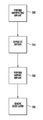
FIG. 2 shows a flowchart of the processes illustrated in FIGS. 1A-1F. As shown in Process 200, an amorphizing implant is first performed. As described above, the thickness of the amorphized region on a particular surface is related to the orientation of that surface.
Next, as shown in Process 210, the workpiece is exposed to oxygen, where the amorphized silicon readily converts to silicon oxide, forming an oxide layer on all surfaces of the workpiece. The thickness of the silicon oxide layer may be nearly the same as the thickness of the previously created amorphized regions. Thus, the thickness of the oxide layer on a particular surface is also related to the orientation of that surface.
After exposure to oxygen, an implant of a dopant species is then performed, as shown in Process 220. As described above, the ions of the dopant species that pass through the oxide layer are ultimately implanted in the workpiece.
Finally, as shown in Process 230, the oxide layer is removed. As described above, it may be advantageous to perform one or more processes on the workpiece prior to the removal of the oxide layer. In other words, the workpiece 10 may be subjected to one or more processes after the dopant implant (Process 220) and prior to the removal of the oxide layer (Process 230).
In certain embodiments, the processes described above are performed in a cluster tool, such that the two implants and the exposure to oxygen are performed without breaking vacuum. In certain embodiments, two or more of these processes are performed in the same chamber by changing the feed gas or other process parameters. For example, after performing the amorphizing implant, oxygen may be introduced into the PLAD chamber to form the oxide layer. During this time, the antenna may be disabled. Subsequently, a dopant species may be introduced as the feed gas and the antenna may be activated to perform the dopant implant.
This sequence can be used to create various semiconductor structures, including, but not limited to CIS (CMOS image sensors), STI (shallow trench isolation), DTI (deep trench isolation), power circuits, logic circuits, memory devices or MEMS devices.
While the disclosure describes the creation of an oxide layer using an amorphizing implant, other embodiments are also possible. For example, the oxide layer may be applied by depositing the oxide on the workpiece during a deposition process.
The embodiments described above in the present application may have many advantages. As described above, as geometries get smaller, the ability to conformally dope a structure on a workpiece becomes more beneficial. The present embodiment describes a technique that is self-compensating. Because the amorphized region is created using the same process that is used for the dopant implant (i.e. an implant process within a PLAD implant system), its implant pattern and behavior is similar. In other words, the thickness of the amorphized regions on each surface will be proportional to the energy of the ions that strike that surface. Consequently, the thickness of the oxide layer is variable as a function of surface orientation and is empirically created. Similarly, the depth to which the dopant ions penetrate the workpiece is also a function of the surface orientation. These two implants tend to normalize the effects of surface orientation such that the implanted dopant is conformally doped.
The present disclosure is not to be limited in scope by the specific embodiments described herein. Indeed, other various embodiments of and modifications to the present disclosure, in addition to those described herein, will be apparent to those of ordinary skill in the art from the foregoing description and accompanying drawings. Thus, such other embodiments and modifications are intended to fall within the scope of the present disclosure. Furthermore, although the present disclosure has been described herein in the context of a particular implementation in a particular environment for a particular purpose, those of ordinary skill in the art will recognize that its usefulness is not limited thereto and that the present disclosure may be beneficially implemented in any number of environments for any number of purposes. Accordingly, the claims set forth below should be construed in view of the full breadth and spirit of the present disclosure as described herein.

Claims (17)

What is claimed is:
1. A method of doping a workpiece having at least two surfaces of different orientations, comprising:
applying an oxide layer to the at least two surfaces of the workpiece, where a thickness of the oxide layer on each surface of the workpiece is proportional to an energy at which ions strike that surface during implant and wherein a thickness of the oxide layer is greater on one of the at least two surfaces of the workpiece due to the orientation of the one surface;
performing an implant of a dopant species to the workpiece after the oxide layer has been applied; and
removing the oxide layer after implanting the dopant species.
2. The method of claim 1, wherein the applying is performed by depositing an oxide on the workpiece.
3. The method of claim 1, wherein the applying comprises:
performing an amorphizing implant to the workpiece; and
exposing the workpiece to oxygen after the amorphizing implant to create an oxide layer.
4. The method of claim 3, wherein the amorphizing implant is performing using germanium, xenon or argon.
5. A method of doping a workpiece, comprising:
amorphizing portions of the workpiece by implanting a first species into the workpiece, wherein implanted portions of the workpiece become amorphized regions and a remainder of the workpiece remains crystalline;
exposing the workpiece to oxygen after the amorphizing, wherein the amorphized regions of the workpiece are converted to a silicon oxide layer, wherein a thickness of the silicon oxide layer is greater on certain surfaces of the workpiece based on orientation of the surfaces;
implanting a dopant species into the workpiece after the exposing such that the dopant species travel through the silicon oxide layer to reach a crystalline portion of the workpiece disposed beneath the silicon oxide layer; and
removing the silicon oxide layer.
6. The method of claim 5, further comprising applying a mask to one or more surfaces of the workpiece prior to the amorphizing.
7. The method of claim 5, wherein a thickness of the silicon oxide layer on a surface of the workpiece is proportional to an energy at which the first species is implanted into that surface.
8. The method of claim 5, further comprising subjecting the workpiece to a thermal treatment after the implanting.
9. The method of claim 8, wherein the thermal treatment is performed prior to the removing.
10. The method of claim 5, wherein a depth and concentration of dopant species that is implanted in the crystalline portion of the workpiece are substantially equal for all surfaces of the workpiece.
11. The method of claim 5, wherein the first species comprises germanium, xenon argon, helium or hydrogen.
12. A method of creating a conformally doped structure on a workpiece, comprising:
amorphizing at least one horizontal surface and at least one non-horizontal surface of a structure on a workpiece by implanting a first species into the structure, wherein implanted regions of the structure become amorphized regions and a remainder of the structure remains crystalline;
exposing the structure to oxygen after the amorphizing, wherein the amorphized regions of the structure are converted to a silicon oxide layer;
implanting a dopant species into the structure after the exposing such that ions of the dopant species travel through the silicon oxide layer to reach a crystalline portion of the structure disposed beneath the silicon oxide layer; and
removing the silicon oxide layer from the structure.
13. The method of claim 12, wherein a thickness of the silicon oxide layer on the at least one horizontal surface is greater than a thickness of the silicon oxide layer on the at least one non-horizontal surface.
14. The method of claim 12, wherein the structure has desired dimensions and the structure is formed having dimensions different than the desired dimensions to account for removal of the silicon oxide layer.
15. The method of claim 12, further comprising subjecting the workpiece to a thermal treatment after the implanting.
16. The method of claim 15, wherein the thermal treatment is performed prior to the removing.
17. The method of claim 12, wherein a depth and concentration of dopant species that are implanted in the crystalline portion of the workpiece disposed beneath the silicon oxide layer is substantially equal for all surfaces.
US14/840,932 2015-08-31 2015-08-31 Self-compensating oxide layer Active US9437432B1 (en)

Priority Applications (1)

Application Number Priority Date Filing Date Title
US14/840,932 US9437432B1 (en) 2015-08-31 2015-08-31 Self-compensating oxide layer

Applications Claiming Priority (1)

Application Number Priority Date Filing Date Title
US14/840,932 US9437432B1 (en) 2015-08-31 2015-08-31 Self-compensating oxide layer

Publications (1)

Publication Number Publication Date
US9437432B1 true US9437432B1 (en) 2016-09-06

Family

ID=56878275

Family Applications (1)

Application Number Title Priority Date Filing Date
US14/840,932 Active US9437432B1 (en) 2015-08-31 2015-08-31 Self-compensating oxide layer

Country Status (1)

Country Link
US (1) US9437432B1 (en)

Citations (2)

* Cited by examiner, † Cited by third party
Publication number Priority date Publication date Assignee Title
US20030219940A1 (en) * 2002-03-07 2003-11-27 Masahiro Hayashi Method for manufacturing semiconductor device
US8778786B1 (en) * 2012-05-29 2014-07-15 Suvolta, Inc. Method for substrate preservation during transistor fabrication

Patent Citations (2)

* Cited by examiner, † Cited by third party
Publication number Priority date Publication date Assignee Title
US20030219940A1 (en) * 2002-03-07 2003-11-27 Masahiro Hayashi Method for manufacturing semiconductor device
US8778786B1 (en) * 2012-05-29 2014-07-15 Suvolta, Inc. Method for substrate preservation during transistor fabrication

Similar Documents

Publication Publication Date Title
JP6629312B2 (en) Method and apparatus for selective deposition
Cheung Plasma immersion ion implantation for semiconductor processing
US9773675B2 (en) 3D material modification for advanced processing
KR102635849B1 (en) DRAM device and method of forming same, and method of forming gate oxide layer
KR20200053623A (en) High Energy ALE (ATOMIC LAYER ETCHING)
TW201246367A (en) Method of etching a workpiece
US20090227096A1 (en) Method Of Forming A Retrograde Material Profile Using Ion Implantation
US8598025B2 (en) Doping of planar or three-dimensional structures at elevated temperatures
TWI665735B (en) Conversion process utilized for manufacturing advanced 3d features for semiconductor device applications
TWI524391B (en) Method for improving conformal doping in a P3I chamber
TW201123274A (en) A technique for processing a substrate having a non-planar surface
US9093367B2 (en) Methods of forming doped regions in semiconductor substrates
US9437432B1 (en) Self-compensating oxide layer
KR100908820B1 (en) Plasma doping method and manufacturing method of semiconductor device using same
US9337314B2 (en) Technique for selectively processing three dimensional device
US20110300696A1 (en) Method for damage-free junction formation
Kim et al. Ultra-shallow junction formation on 3D silicon and germanium device structures by ion energy decoupled plasma doping
Paeng et al. Enhancing phosphorous doping level on Ge by Sb co-doping with non-beamline implantation methods
KR101211041B1 (en) Method for manufacturing semiconductor device improved etch uniformity
JPH03270222A (en) Ion-implantation in semiconductor

Legal Events

Date Code Title Description
AS Assignment

Owner name: VARIAN SEMICONDUCTOR EQUIPMENT ASSOCIATES, INC., M

Free format text: ASSIGNMENT OF ASSIGNORS INTEREST;ASSIGNORS:MAYNARD, HELEN L.;MITTAL, DEVEN RAJ;LEE, JUN SEOK;REEL/FRAME:036634/0525

Effective date: 20150915

STCF Information on status: patent grant

Free format text: PATENTED CASE

MAFP Maintenance fee payment

Free format text: PAYMENT OF MAINTENANCE FEE, 4TH YEAR, LARGE ENTITY (ORIGINAL EVENT CODE: M1551); ENTITY STATUS OF PATENT OWNER: LARGE ENTITY

Year of fee payment: 4

MAFP Maintenance fee payment

Free format text: PAYMENT OF MAINTENANCE FEE, 8TH YEAR, LARGE ENTITY (ORIGINAL EVENT CODE: M1552); ENTITY STATUS OF PATENT OWNER: LARGE ENTITY

Year of fee payment: 8