US9425850B2 - Simultaneous voice and data communication - Google Patents
Simultaneous voice and data communication Download PDFInfo
- Publication number
- US9425850B2 US9425850B2 US13/282,221 US201113282221A US9425850B2 US 9425850 B2 US9425850 B2 US 9425850B2 US 201113282221 A US201113282221 A US 201113282221A US 9425850 B2 US9425850 B2 US 9425850B2
- Authority
- US
- United States
- Prior art keywords
- data
- voice
- signal
- multiplexer
- receive
- Prior art date
- Legal status (The legal status is an assumption and is not a legal conclusion. Google has not performed a legal analysis and makes no representation as to the accuracy of the status listed.)
- Expired - Fee Related, expires
Links
Images


Classifications
-
- H—ELECTRICITY
- H04—ELECTRIC COMMUNICATION TECHNIQUE
- H04B—TRANSMISSION
- H04B1/00—Details of transmission systems, not covered by a single one of groups H04B3/00 - H04B13/00; Details of transmission systems not characterised by the medium used for transmission
- H04B1/38—Transceivers, i.e. devices in which transmitter and receiver form a structural unit and in which at least one part is used for functions of transmitting and receiving
- H04B1/40—Circuits
- H04B1/403—Circuits using the same oscillator for generating both the transmitter frequency and the receiver local oscillator frequency
- H04B1/406—Circuits using the same oscillator for generating both the transmitter frequency and the receiver local oscillator frequency with more than one transmission mode, e.g. analog and digital modes
-
- H—ELECTRICITY
- H04—ELECTRIC COMMUNICATION TECHNIQUE
- H04B—TRANSMISSION
- H04B1/00—Details of transmission systems, not covered by a single one of groups H04B3/00 - H04B13/00; Details of transmission systems not characterised by the medium used for transmission
- H04B1/38—Transceivers, i.e. devices in which transmitter and receiver form a structural unit and in which at least one part is used for functions of transmitting and receiving
- H04B1/40—Circuits
- H04B1/50—Circuits using different frequencies for the two directions of communication
- H04B1/52—Hybrid arrangements, i.e. arrangements for transition from single-path two-direction transmission to single-direction transmission on each of two paths or vice versa
- H04B1/525—Hybrid arrangements, i.e. arrangements for transition from single-path two-direction transmission to single-direction transmission on each of two paths or vice versa with means for reducing leakage of transmitter signal into the receiver
Definitions
- the present disclosure relates generally to electronic devices for communication systems. More specifically, the present disclosure relates to systems and methods for simultaneous voice and data communication.
- Electronic devices have become a part of everyday life. Small computing devices are now placed in everything from automobiles to housing locks. The complexity of electronic devices has increased dramatically in the last few years. For example, many electronic devices have one or more processors that help control the device, as well as a number of digital circuits to support the processor and other parts of the device.
- Electronic devices may communicate wireless with each other and with a network.
- Electronic devices may provide many different types of communication. For example, some electronic devices provide voice communication while other electronic devices provide data communication. Some electronic devices now provide both voice communication and data communication. Benefits may be realized by providing improved systems and methods to implement simultaneous voice and data communications for electronic devices.
- the wireless device includes a voice and data transceiver.
- the voice and data transceiver includes data path circuitry, voice path circuitry, a first diplexer and a second diplexer.
- the first diplexer sends a primary data receive signal to the data path circuitry and receives a data transmit signal from the data path circuitry.
- the second diplexer sends a diversity data receive signal to the data path circuitry, sends a voice receive signal to the voice path circuitry and receives a voice transmit signal from the voice path circuitry.
- the wireless device also includes a first antenna coupled to the first diplexer and a second antenna coupled to the second diplexer.
- the first diplexer and the second diplexer may reduce third order intermodulation interference introduced in the voice and data transceiver.
- the wireless device may be a wireless communication device configured to operate using a Long Term Evolution standard.
- the data path circuitry may include a primary data receive chain, a data transmit chain and a diversity data receive chain.
- the voice path circuitry may include a voice receive chain and a voice transmit chain.
- the wireless device includes a voice and data transceiver.
- the voice and data transceiver includes data path circuitry, voice path circuitry, a first diplexer and a second diplexer.
- the first diplexer sends a primary data receive signal to the data path circuitry, receives a data transmit signal from the data path circuitry and sends a voice receive signal to the voice path circuitry.
- the second diplexer sends a diversity data receive signal to the data path circuitry and receives a voice transmit signal from the voice path circuitry.
- the wireless device also includes a first antenna coupled to the first diplexer and a second antenna coupled to the second diplexer.
- the wireless device includes a voice and data transceiver.
- the voice and data transceiver includes data path circuitry, voice path circuitry, a first diplexer and a second diplexer.
- the first diplexer sends a diversity data receive signal to the data path circuitry, receives a data transmit signal from the data path circuitry and sends a voice receive signal to the voice path circuitry.
- the second diplexer sends a primary data receive signal to the data path circuitry and receives a voice transmit signal from the voice path circuitry.
- the wireless device also includes a first antenna coupled to the first diplexer and a second antenna coupled to the second diplexer.
- a method for simultaneous voice and data communication is described.
- a voice signal is communicated.
- a data signal is also communicated.
- Third order intermodulation interference generated by simultaneously communicating the voice signal and the data signal is minimized
- the voice signal may be communicated using a first antenna and a first diplexer.
- the voice signal and the data signal may be transmitted simultaneously.
- Communicating the voice signal may include receiving the voice signal.
- Communicating the data signal may include receiving the data signal.
- the voice signal and the data signal may be received simultaneously.
- the method may be performed by a wireless communication device.
- the wireless device includes a voice and data transceiver.
- the voice and data transceiver includes data path circuitry, voice path circuitry, a first diplexer and a second diplexer.
- the first diplexer sends a primary data receive signal to the data path circuitry, receives a voice transmit signal from the voice path circuitry and receives a data transmit signal from the data path circuitry.
- the second diplexer sends a diversity data receive signal to the data path circuitry and sends a voice receive signal to the voice path circuitry.
- the voice and data transceiver also includes a duplexer that is coupled between the second diplexer and a data modem.
- the voice and data transceiver further includes a resistor that is coupled between the duplexer and ground.
- the wireless device also includes a first antenna coupled to the first diplexer and a second antenna coupled to the second diplexer.
- the configuration of the duplexer and the resistor may be such that the duplexer is used as a diversity receive signal filter.
- the data transmit signal may be terminated at the resistor such that it does not reflect back to the duplexer to generate third order intermodulation interference with the voice transmit signal.
- the resistor may be a 50 ohm resistor.
- the apparatus includes means for communicating a voice signal.
- the apparatus also includes means for communicating a data signal.
- the apparatus further includes means for minimizing third order intermodulation interference generated by simultaneously communicating the voice signal and the data signal.
- the means for communicating the voice signal may include using a first antenna and a first diplexer.
- the means for communicating the data signal may include the first antenna, the first diplexer, a second antenna and a second diplexer. Communicating the voice signal may include transmitting the voice signal. Communicating the data signal may include transmitting the data signal. The voice signal and the data signal may be transmitted simultaneously.
- Communicating the voice signal may include receiving the voice signal.
- Communicating the data signal may include receiving the data signal.
- the voice signal and the data signal may be received simultaneously.
- the apparatus may be a wireless communication device.
- FIG. 1 shows a wireless communication system 100 with multiple wireless devices
- FIG. 2 is a block diagram illustrating a simultaneous voice and data (SVD) transceiver for use in the present systems and methods;
- SVD simultaneous voice and data
- FIG. 3 is a block diagram illustrating another simultaneous voice and data (SVD) transceiver for use in the present systems and methods;
- FIG. 4 is a block diagram illustrating a front-end architecture of a simultaneous voice and data (SVD) transceiver
- FIG. 5 is a flow diagram of a method for simultaneous voice and data communication with reduced third order intermodulation (IM3) interference;
- IM3 third order intermodulation
- FIG. 6 is a flow diagram of a method for receiving and transmitting voice signals and data signals simultaneously
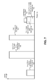
- FIG. 7 illustrates the desensitization that may occur during simultaneous voice and data (SVD) communications
- FIG. 8 illustrates the proposed radio frequency (RF) front-end architecture to mitigate the third order intermodulation (IM3) interference issue
- FIG. 9 illustrates certain components that may be included within a wireless communication device.
- 3GPP The 3 rd Generation Partnership Project
- 3GPP Long Term Evolution (LTE) is a 3GPP project aimed at improving the Universal Mobile Telecommunications System (UMTS) mobile phone standard.
- UMTS Universal Mobile Telecommunications System
- the 3GPP may define specifications for the next generation of mobile networks, mobile systems and mobile devices.
- a mobile station or device may be referred to as a “user equipment” (UE).
- UE user equipment
- 3GPP specifications are based on evolved Global System for Mobile Communications (GSM) specifications, which are generally known as the Universal Mobile Telecommunications System (UMTS). 3GPP standards are structured as releases. Discussion of 3GPP thus frequently refers to the functionality in one release or another.
- GSM Global System for Mobile Communications
- UMTS Universal Mobile Telecommunications System
- Release 99 specifies the first UMTS third generation (3G) networks, incorporating a CDMA air interface.
- Release 6 integrates operation with wireless local area networks (LAN) networks and adds High Speed Uplink Packet Access (HSUPA).
- Release 8 introduces dual downlink carriers and Release 9 extends dual carrier operation to uplink for UMTS.
- CDMA2000 is a family of third generation (3G) technology standards that use code division multiple access (CDMA) to send voice, data and signaling between wireless devices.
- CDMA2000 may include CDMA2000 1X, CDMA2000 EV-DO Rev. 0, CDMA2000 EV-DO Rev. A and CDMA2000 EV-DO Rev. B.
- 1x or 1xRTT refers to the core CDMA2000 wireless air interface standard. 1x more specifically refers to 1 times Radio Transmission Technology and indicates the same radio frequency (RF) bandwidth as used in IS-95. 1xRTT adds 64 additional traffic channels to the forward link.
- EV-DO refers to Evolution-Data Optimized.
- EV-DO is a telecommunications standard for the wireless transmission of data through radio signals.
- FIG. 1 shows a wireless communication system 100 with multiple wireless devices.
- a wireless device may be a base station 102 , a wireless communication device 104 , a controller, or the like.
- a base station 102 is a station that communicates with one or more wireless communication devices 104 .
- a base station 102 may also be referred to as, and may include some or all of the functionality of, an access point, a broadcast transmitter, a Node B, an evolved Node B, etc.
- Each base station 102 provides communication coverage for a particular geographic area.
- a base station 102 may provide communication coverage for one or more wireless communication devices 104 .
- the term “cell” can refer to a base station 102 and/or its coverage area depending on the context in which the term is used. Each cell may be further divided into sectors. A base station 102 may thus cover multiple sectors.
- a wireless communication device 104 may also be referred to as, and may include some or all of the functionality of, a terminal, an access terminal, a user equipment (UE), a subscriber unit, a station, etc.
- a wireless communication device 104 may be a cellular phone, a personal digital assistant (PDA), a wireless device, a wireless modem, a handheld device, a laptop computer, a PC card, compact flash, an external or internal modem, a wireline phone, etc.
- a wireless communication device 104 may be mobile or stationary.
- a wireless communication device 104 may communicate with zero, one or multiple base stations 102 on a downlink 106 and/or an uplink 108 at any given moment.
- the downlink 106 (or forward link) refers to the communication link from a base station 102 to a wireless communication device 104
- the uplink 108 (or reverse link) refers to the communication link from a wireless communication device 104 to a base station 102
- Uplink 108 and downlink 106 may refer to the communication link or to the carriers used for the communication link.
- the wireless communication system 100 may be a multiple-access system capable of supporting communication with multiple wireless communication devices 104 by sharing the available system resources (e.g., bandwidth and transmit power).
- multiple-access systems include code division multiple access (CDMA) systems, wideband code division multiple access (W-CDMA) systems, time division multiple access (TDMA) systems, frequency division multiple access (FDMA) systems, orthogonal frequency division multiple access (OFDMA) systems and spatial division multiple access (SDMA) systems.
- CDMA code division multiple access
- W-CDMA wideband code division multiple access
- TDMA time division multiple access
- FDMA frequency division multiple access
- OFDMA orthogonal frequency division multiple access
- SDMA spatial division multiple access
- a wireless communication network 100 may provide communication for a number of wireless communication devices 104 , each of which may be serviced by a base station 102 .
- Wireless communication networks 100 that use CDMA2000 for voice and Data Optimized (DO) for data may be unable to provide simultaneous voice and data (SVD) to consumers.
- a base station 102 may be unable to provide both data and voice services simultaneously to a wireless communication device 104 .
- One main reason for this inability is the large amounts of interference that may occur during simultaneous voice and data (SVD) transmission.
- a wireless communication device 104 may need a simultaneous voice and data (SVD) transceiver 110 .
- the design of the simultaneous voice and data (SVD) transceiver 110 may be such that third order intermodulation (IM3) interference reduction is needed.
- the simultaneous voice and data (SVD) transceiver 110 may be designed to minimize the third order intermodulation (IM3) interference generated without increasing the number of antennas on the wireless communication device 104 .
- a wireless communication device 104 may have two antennas; thus, it may be desirable to provide simultaneous voice and data (SVD) for LTE with two antennas. Examples of simultaneous voice and data (SVD) systems include 1xCDMA voice +LTE/DO/TDSCDMA data, GSM voice +LTE/WCDMA/TDSCDMA data and UMTS voice +LTE/TDSCDMA data.
- the data transmit signal (Tx 1 ), the primary data receive signal(PRx), the voice transmit signal (Tx 2 ) and the voice receive signal(Rx) use a first antenna while the diversity data receive signal (DRx) uses a second antenna.
- the third order intermodulation (IM3) interference for data I IM3(data) is illustrated in Equation (1): I IM3(data) ⁇ ( Tx 1) 2 *Tx 2.
- Equation (2) The third order intermodulation (IM3) interference for voice I IM3(voice) is illustrated in Equation (2): I IM3(voice) ⁇ Tx 1*( Tx 2) 2 . (2)
- IM3 interference level is the strongest with both data and voice transmitted signals are at or near their maximum.
- SAR Standard Absorption Rate
- FIG. 2 is a block diagram illustrating a simultaneous voice and data (SVD) transceiver 210 for use in the present systems and methods.
- the simultaneous voice and data (SVD) transceiver 210 of FIG. 2 may be one configuration of the simultaneous voice and data (SVD) transceiver 110 of FIG. 1 .
- the simultaneous voice and data (SVD) transceiver 210 may be designed such that there is reduced third order intermodulation (IM3) interference.
- IM3 third order intermodulation
- the simultaneous voice and data (SVD) transceiver 210 may be located on a wireless communication device 104 with a first antenna 214 a and a second antenna 214 b .
- the simultaneous voice and data (SVD) transceiver 210 may be coupled to both the first antenna 214 a and the second antenna 214 b.
- the simultaneous voice and data (SVD) transceiver 210 may include data path circuitry 226 and voice path circuitry 228 . Both data signals and voice signals may be input and output from the data path circuitry 226 . Also, both data and voice signals may be input and output from the voice path circuitry 228 .
- the data path circuitry 226 may be coupled to a first multiplexer 216 a .
- a multiplexer 216 may be a passive device that implements frequency domain multiplexing. In one configuration, the multiplexers 216 used herein may be diplexers.
- the first multiplexer 216 a may be coupled to the first antenna 214 a .
- Signals between the data path circuitry 226 and the first multiplexer 216 a may include a primary data receive signal (PRx) 241 and a data transmit signal (Tx 1 ) 242 .
- PRx primary data receive signal
- Tx 1 data transmit signal
- one or more additional antennas 214 may be used to improve the quality and reliability of a wireless link.
- the wireless communication device 104 may receive a data signal over each antenna 214 .
- One of these data signals may be a primary data signal while the other is a diversity data signal.
- the primary data receive signal (PRx) 241 may be the data signal that has the highest signal-to-noise ratio (SNR) (compared to the diversity data receive signal (DRx) 222 ).
- SNR signal-to-noise ratio
- the primary data receive signal (PRx) 241 may be the data signal that is received by the primary antenna 214 (i.e., the first antenna 214 a ) and the diversity data receive signal (DRx) 222 may be the data signal received by a secondary antenna 214 (i.e., the second antenna 214 b ).
- the data path circuitry 226 may also be coupled to a second multiplexer 216 b .
- the second multiplexer 216 b may be coupled to the second antenna 214 b .
- Signals between the data path circuitry 226 and the second multiplexer 216 b may include a diversity data receive signal (DRx) 222 .
- the voice path circuitry 228 may be coupled to the second multiplexer 216 b .
- Signals between the voice path circuitry 228 and the second multiplexer 216 b may include a voice receive signal (Rx) 220 and a voice transmit signal (Tx 2 ) 224 .
- the third order intermodulation (IM3) interference for data I IM3(data) is illustrated in Equation (3): I IM3(data) ⁇ ( Tx 1) 2 *( ⁇ * Tx 2).
- the third order intermodulation (IM3) interference for voice I IM3(voice) may be illustrated using Equation (4): I IM3(voice) ⁇ ( ⁇ * Tx 1)*( Tx 2) 2 . (4)
- Equation (3) and Equation (4) represent a reduction in the baseline third order intermodulation (IM3) interference (i.e., the third order intermodulation (IM3) interference from Equation (1) and Equation (2) above) of a , which is around ⁇ 10 decibels (dB) for practical designs.
- IM3 interference i.e., the third order intermodulation (IM3) interference from Equation (1) and Equation (2) above
- the data path circuitry 226 may receive data for transmission 230 .
- the data path circuitry 226 may forward received data 232 for use by the wireless communication device 104 .
- the voice path circuitry 228 may receive voice for transmission 234 .
- the voice path circuitry 228 may forward received voice 236 for use by the wireless communication device 104 .
- FIG. 3 is a block diagram illustrating another simultaneous voice and data (SVD) transceiver 310 for use in the present systems and methods.
- the simultaneous voice and data (SVD) transceiver 310 of FIG. 3 may be one configuration of the simultaneous voice and data (SVD) transceiver 110 of FIG. 1 .
- the simultaneous voice and data (SVD) transceiver 310 may be designed such that there is further reduced third order intermodulation (IM3) interference in comparison to previous configurations.
- IM3 third order intermodulation
- the simultaneous voice and data (SVD) transceiver 310 may be located on a wireless communication device 104 with a first antenna 314 a and a second antenna 314 b .
- the simultaneous voice and data (SVD) transceiver 310 may be coupled to both the first antenna 314 a and the second antenna 314 b.
- the simultaneous voice and data (SVD) transceiver 310 may include data path circuitry 326 and voice path circuitry 328 . Both data signals and voice signals may be input and output from the data path circuitry 326 . Also, both data and voice signals may be input and output from the voice path circuitry 328 .
- the data path circuitry 326 may be coupled to a first multiplexer 316 a .
- the first multiplexer 316 a may be coupled to the first antenna 314 a .
- Signals between the data path circuitry 326 and the first multiplexer 316 a may include a primary data receive signal (PRx) 341 and a data transmit signal (Tx 1 ) 342 .
- PRx primary data receive signal
- Tx 1 data transmit signal
- the data path circuitry 326 may also be coupled to a second multiplexer 316 b .
- the second multiplexer 316 b may be coupled to the second antenna 314 b .
- Signals between the data path circuitry 326 and the second multiplexer 316 b may include a diversity data receive signal (DRx) 322 .
- DRx diversity data receive signal
- the voice path circuitry 328 may be coupled to both the first multiplexer 316 a and the second multiplexer 316 b . Signals between the voice path circuitry 328 and the first multiplexer 316 a may include a voice receive signal (Rx) 320 . Signals between the voice path circuitry 328 and the second multiplexer 316 b may include a voice transmit signal (Tx 2 ) 324 .
- Rx voice receive signal
- Tx 2 voice transmit signal
- the third order intermodulation (IM3) interference for voice I IM3(voice) may be illustrated using Equation (5): I IM3(voice) ⁇ 2* ⁇ *( ⁇ * Tx 1)*( Tx 2) 2 . (5)
- Equation (5) represents a reduction in the baseline third order intermodulation (IM3) interference (i.e., the third order intermodulation (IM3) interference from Equation (1)) of 2 ⁇ 2 , which is ⁇ 17 dB.
- the third order intermodulation (IM3) interference for data for the primary data receive signal (PRx) 341 has a reduction factor of ( ⁇ + ⁇ 3 ) ⁇ , which is ⁇ 10 dB.
- the data path circuitry 326 may receive data for transmission 330 .
- the data path circuitry 326 may forward received data 332 for use by the wireless communication device 104 .
- the voice path circuitry 328 may receive voice for transmission 334 .
- the voice path circuitry 328 may forward received voice 336 for use by the wireless communication device 104 .
- FIG. 4 is a block diagram illustrating a front-end architecture of a simultaneous voice and data (SVD) transceiver 510 .
- the simultaneous voice and data (SVD) transceiver 510 of FIG. 4 may be one configuration of the simultaneous voice and data (SVD) transceiver 110 of FIG. 1 .
- the simultaneous voice and data (SVD) transceiver 510 may be designed such that there is reduced third order intermodulation (IM3) interference.
- IM3 third order intermodulation
- a first antenna 514 a may be coupled to a first multiplexer 516 a .
- the first multiplexer 516 a may be a diplexer.
- the first antenna 514 a may be used for a primary data receive (PRx) chain 543 , a data transmit (Tx 1 ) chain 546 and a voice receive (Rx) chain 552 .
- a second antenna 514 b may be coupled to a second multiplexer 516 b .
- the second multiplexer 516 b may be a diplexer.
- the second antenna 514 b may be used for a diversity data receive (DRx) 549 chain and a voice transmit (Tx 2 ) chain 555 .
- the primary data receive (PRx) chain 543 , data transmit (Tx 1 ) 546 chain and diversity data receive (DRx) chain 549 may each be a part of a data path circuitry 526 .
- the primary data receive (PRx) chain 543 may include a receiver 544 and a demodulator 545 .
- the demodulator 545 may be part of a modem.
- the data transmit (Tx 1 ) chain 546 may include a transmitter 547 and a modulator 548 .
- the modulator 548 may be part of a modem.
- the diversity data receive (DRx) chain 549 may include a receiver 550 and a demodulator 551 .
- the demodulator 551 may be part of a modem.
- the voice receive (Rx) chain 552 and the voice transmit (Tx 2 ) chain 555 may be part of a voice path circuitry 528 .
- the voice receive (Rx) chain 552 may include a receiver 553 and a demodulator 554 .
- the demodulator 554 may be part of a modem.
- the voice transmit (Tx 2 ) chain 555 may include a transmitter 556 and a modulator 557 .
- the modulator 557 may be part of a modem.
- the first multiplexer 516 a may send a primary data receive signal (PRx) 541 to the primary data receive (PRx) chain 543 in the data path circuitry 526 .
- the first multiplexer 516 a may also send a voice receive signal (Rx) 520 to the voice receive (Rx) chain 552 in the voice path circuitry 528 .
- the first multiplexer 516 a may receive a data transmit signal (Tx 1 ) 542 from the data transmit (Tx 1 ) chain 546 .
- the second multiplexer 516 b may send a diversity data receive signal (DRx) 522 to the diversity data receive (DRx) chain 549 in the data path circuitry 526 .
- the second multiplexer 516 b may receive a voice transmit signal (Tx 2 ) 524 from the voice transmit (Tx 2 ) chain 555 in the voice path circuitry 528 .
- a signal between the first antenna 514 a and the first multiplexer 516 a may be a first composite signal 521 a that includes at least one of the primary data receive signal (PRx) 541 , the data transmit signal (Tx 1 ) 542 and the voice receive signal (Rx) 520 .
- a signal between the second antenna 514 b and the second multiplexer 516 b may be a second composite signal 521 b that includes at least one of the diversity data receive signal (DRx) 522 and the voice transmit signal (Tx 2 ) 524 .
- FIG. 5 is a flow diagram of a method 600 for simultaneous voice and data communication with reduced third order intermodulation (IM3) interference.
- the method 600 may be performed by a wireless communication device 104 .
- the wireless communication device 104 may communicate 602 a voice signal.
- the wireless communication device 104 may communicate 602 the voice signal using a first multiplexer 316 a , a first antenna 314 a coupled to the first multiplexer 316 a , a second multiplexer 316 b and a second antenna 314 b coupled to the second multiplexer 316 b .
- the wireless communication device 104 may communicate 602 the voice signal using only a multiplexer 216 b and an antenna 214 b coupled to the multiplexer 216 b .
- Communicating 602 a voice signal may include both receiving a voice receive signal (Rx) 220 and transmitting a voice transmit signal (Tx 2 ) 224 .
- communicating 602 a voice signal may include receiving a voice receive signal (Rx) 220 while simultaneously transmitting a voice transmit signal (Tx 2 ) 224 .
- the wireless communication device 104 may also communicate 604 a data signal.
- the wireless communication device 104 may communicate a data signal using a first multiplexer 216 a , a first antenna 214 a coupled to the first multiplexer 216 a , a second multiplexer 216 b and a second antenna 214 b coupled to the second multiplexer 216 b .
- Communicating 604 a data signal may include receiving a primary data receive signal (PRx) 241 , receiving a diversity data receive signal (DRx) 222 and sending a data transmit signal (Tx 1 ) 242 .
- communicating 604 a data signal may include receiving a primary data receive signal (PRx) 241 and a diversity data receive signal (DRx) 222 while simultaneously transmitting a data transmit signal (Tx 1 ) 242 .
- the wireless communication device 104 may communicate 602 the voice signal while simultaneously communicating 604 the data signal.
- the wireless communication device 104 may receive a primary data receive signal (PRx) 241 , a diversity data receive signal (DRx) 222 and a voice receive signal (Rx) 220 while simultaneously transmitting a data transmit signal (Tx 1 ) 242 and a voice transmit signal (Tx 2 ) 224 .
- the wireless communication device 104 may minimize 606 third order intermodulation (IM3) interference generated by simultaneously communicating the voice signal and the data signal.
- the design of the wireless communication device 104 may minimize 606 third order intermodulation (IM3) interference.
- FIG. 6 is a flow diagram of a method 700 for receiving and transmitting voice signals and data signals simultaneously.
- the method 700 may be performed by a wireless communication device 104 .
- the wireless communication device 104 may include a simultaneous voice and data (SVD) transceiver 310 (with reduced third order intermodulation (IM3) interference).
- the wireless communication device 104 may receive 702 a diversity data receive signal (DRx) 322 using a first antenna 314 a and a first multiplexer 316 a .
- the wireless communication device 104 may also receive 704 a voice receive signal (Rx) using the first multiplexer 316 a and the first antenna 314 a.
- DRx diversity data receive signal
- Rx voice receive signal
- the wireless communication device 104 may further receive 706 a primary data receive signal (PRx) 341 using a second multiplexer 316 b and a second antenna 314 b .
- the wireless communication device 104 may transmit 708 a data transmit signal (Tx 1 ) 342 using the first multiplexer 316 a and the first antenna 314 a .
- the wireless communication device 104 may also transmit 710 a voice transmit signal (Tx 2 ) 324 using the second multiplexer 316 b and the second antenna 314 b .
- the configuration of the first multiplexer 316 a and the second multiplexer 316 b may be such that third order intermodulation (IM3) interference introduced is reduced when compared to traditional configurations.
- the third order intermodulation (IM3) interference introduced may be reduced by ⁇ 17 dB for the voice and ⁇ 17 dB for the data compared to traditional configurations.
- FIG. 7 illustrates the desensitization that may occur during simultaneous voice and data (SVD) communications.
- a graph of frequency versus signal strength is shown. It is not certain when Voice over Internet Protocol (VOIP) will become ubiquitous.
- VOIP Voice over Internet Protocol
- a dedicated chain for data LTE, DO, WLAN, etc.
- a second chain for voice may be used along with a second chain for voice to cope with issues arising from dual transmissions. Intermodulation between the two transmission chains (the data transmission chain and the voice transmission chain) can lead to performance degradation (e.g., sensitivity, spurious emissions). This can result in challenges to meet the Federal Communication Commission (FCC) specific absorption rate (SAR) requirements.
- FCC Federal Communication Commission
- SAR specific absorption rate
- SSLTE Voice Long Term Evolution
- B13 Band 13
- BC0 Band 0
- IM3 third order intermodulation
- This desensitization occurs when both the Long Term Evolution (LTE) transmit signals 759 and the BCO transmit signals (cell transmission (Tx) signal 760 ) are at or near maximum power, making it difficult to pass carrier certification testing.
- WCDMA Wideband Code Division Multiple Access
- SVD simultaneous voice and data
- the third order intermodulation (IM3) interference 762 may dominate the cell receive (Rx) signal 761 when using simultaneous voice and data communications, limiting the effectiveness of simultaneous voice and data (SVD) communications.
- IM3 simultaneous voice and data
- IM3 reduced third order intermodulation
- LTE long term evolution
- the frequencies and relative signal strengths of the Long Term Evolution (LTE) receive (Rx) signal 758 , the Long Term Evolution (LTE) transmission (Tx) signal 759 , the cell transmission (Tx) signal 760 and the cell receive (Rx) signal 761 are shown.
- the frequencies and signal strengths are not drawn to scale and are illustrated only to show where the third order intermodulation (IM3) interference 762 falls on the frequency spectrum (and how this third order intermodulation (IM3) interference 762 is reduced).
- FIG. 8 illustrates the proposed radio frequency (RF) front-end architecture to mitigate the third order intermodulation (IM3) interference issue.
- a first antenna 814 a may be used for the primary data receive (PRx) chain 543 , the data transmit (Tx 1 ) chain 546 and the voice receive (Rx) chain 552 .
- a second antenna 814 b may be used for the voice transmit (Tx 2 ) chain 555 and the diversity data receive (DRx) chain 549 .
- a first multiplexer 816 a may be coupled to the first antenna 814 a .
- the first multiplexer 816 a may be coupled to a first duplexer 864 a and a second duplexer 864 b .
- a duplexer 864 is a device that allows bi-directional communication over a single channel.
- the first duplexer 864 a may output a primary data receive signal (PRx) 841 to a data modem 868 .
- the second duplexer 864 b may receive a data optimized (DO) transmit signal (Tx 1 ) 842 from the data modem 868 .
- the second duplexer 864 b may also output a voice receive signal (Rx) 820 via a switch 867 a to a voice and global positioning system (GPS) modem 870 .
- PRx primary data receive signal
- Tx 1 data optimized transmit signal
- the first multiplexer 816 a may also be coupled to a third duplexer 864 c .
- the third duplexer 864 c may receive a data optimized (DO) transmit signal from the data modem 868 and generate a personal communications system (PCS) receive signal (Rx).
- the personal communications system (PCS) receive signal (Rx) may be output to a switch 867 b that then outputs either a data optimized (DO) receive signal to the data modem 868 or a 1 x receive signal (Rx) to the voice and global positioning system (GPS) modem 870 .
- Signals for transmission may be passed through power amplifiers 866 a - e.
- a second multiplexer 816 b may be coupled to the second antenna 814 b .
- the second multiplexer 816 b may be coupled to a fourth duplexer 864 d and a fifth duplexer 864 e .
- the fourth duplexer 864 d may output a long term evolution (LTE) diversity data receive signal (DRx) 822 to the data modem 868 .
- the fifth duplexer 864 e may receive a 1 x voice transmit signal (Tx 2 ) 824 from the voice and global positioning system (GPS) modem 870 .
- the second multiplexer 816 b may also be coupled to a sixth duplexer 864 f for personal communications service (PCS).
- the voice and global positioning system (GPS) modem 870 may also be coupled to a global positioning system (GPS) antenna 814 c.
- GPS global positioning system
- the fourth duplexer 864 d may be coupled to ground using a 50 Ohm resistor.
- the 50 Ohm resistor is used to terminate the data duplexer transmit signal (Tx 1 ) so that the fourth duplexer 864 d is used as a diversity Rx filter.
- IM3 third order intermodulation
- This results in reduced third order intermodulation (IM3) interference generated by the fourth duplexer 864 d for voice because the data Tx coupling from the first antenna 814 a will contribute less to the generation of third order intermodulation (IM3) interference.
- IM3 third order intermodulation
- IM3 the third order intermodulation (IM3) interference due to the circuitry for the first antenna 814 a ) ⁇ Tx 1 ( ⁇ *Tx 2 ) 2 because Tx 2 is in the second antenna 814 b .
- IM3 2 (the third order intermodulation (IM3) interference due to the circuitry for the second antenna 814 b ) ⁇ ( ⁇ *Tx 1 )*(Tx 2 ) 2 because Tx 1 needs to be coupled to the second antenna 814 b to generate IM3 2 .
- the voice receive (Rx) signal 820 uses the first antenna 814 a
- Tx 1 and Tx 2 in two antennas 814 provides an improvement factor of ⁇ (10 dB) over the combining of Tx 1 and Tx 2 in the same antenna 814 .
- This allows for a better use of the available spectrum and increased flexibility in spectrum planning. It also allows for concurrency of voice and data that the current standard does not support (e.g., SVLTE and SVDO). More security can be imposed on a chosen channel.
- the data requires a primary data receive signal (PRx) 841 and a diversity data receive signal (DRx) 822 to benefit from spatial diversity gain.
- the voice transmit signal (Tx 2 ) 824 may be allocated to the same antenna 814 as the diversity data receive signal (DRx) 822 .
- the voice receive signal (Rx) 820 may be allocated to the same antenna 814 as the primary data receive signal (PRx) 841 .
- the data modem 868 and the voice and global positioning system (GPS) modem 870 may use a high-speed universal asynchronous receiver/transmitter (HS-UART) 871 to communicate with each other.
- the data modem 868 and the voice and global positioning system (GPS) modem 870 may also use a Secure Digital Input Output (SDIO) 872 to communicate with each other.
- SDIO Secure Digital Input Output
- FIG. 9 illustrates certain components that may be included within a wireless communication device 904 .
- the wireless communication device 904 may be an access terminal, a mobile station, a user equipment (UE), etc.
- the wireless communication device 904 includes a processor 903 .
- the processor 903 may be a general purpose single- or multi-chip microprocessor (e.g., an ARM), a special purpose microprocessor (e.g., a digital signal processor (DSP)), a microcontroller, a programmable gate array, etc.
- the processor 903 may be referred to as a central processing unit (CPU).
- CPU central processing unit
- the wireless communication device 904 also includes memory 905 .
- the memory 905 may be any electronic component capable of storing electronic information.
- the memory 905 may be embodied as random access memory (RAM), read-only memory (ROM), magnetic disk storage media, optical storage media, flash memory devices in RAM, on-board memory included with the processor, EPROM memory, EEPROM memory, registers and so forth, including combinations thereof.
- Data 907 a and instructions 909 a may be stored in the memory 905 .
- the instructions 909 a may be executable by the processor 903 to implement the methods disclosed herein. Executing the instructions 909 a may involve the use of the data 907 a that is stored in the memory 905 .
- various portions of the instructions 909 b may be loaded onto the processor 903
- various pieces of data 907 b may be loaded onto the processor 903 .
- the wireless communication device 904 may also include a transmitter 911 and a receiver 913 to allow transmission and reception of signals to and from the wireless communication device 904 via a first antenna 917 a and a second antenna 917 b .
- the transmitter 911 and receiver 913 may be collectively referred to as a transceiver 915 .
- the wireless communication device 904 may also include (not shown) multiple transmitters, additional antennas, multiple receivers and/or multiple transceivers.
- the wireless communication device 904 may include a digital signal processor (DSP) 921 .
- the wireless communication device 904 may also include a communications interface 923 .
- the communications interface 923 may allow a user to interact with the wireless communication device 904 .
- the various components of the wireless communication device 904 may be coupled together by one or more buses, which may include a power bus, a control signal bus, a status signal bus, a data bus, etc.
- buses may include a power bus, a control signal bus, a status signal bus, a data bus, etc.
- the various buses are illustrated in FIG. 9 as a bus system 919 .
- determining encompasses a wide variety of actions and, therefore, “determining” can include calculating, computing, processing, deriving, investigating, looking up (e.g., looking up in a table, a database or another data structure), ascertaining and the like. Also, “determining” can include receiving (e.g., receiving information), accessing (e.g., accessing data in a memory) and the like. Also, “determining” can include resolving, selecting, choosing, establishing and the like.
- processor should be interpreted broadly to encompass a general purpose processor, a central processing unit (CPU), a microprocessor, a digital signal processor (DSP), a controller, a microcontroller, a state machine and so forth.
- a “processor” may refer to an application specific integrated circuit (ASIC), a programmable logic device (PLD), a field programmable gate array (FPGA), etc.
- ASIC application specific integrated circuit
- PLD programmable logic device
- FPGA field programmable gate array
- processor may refer to a combination of processing devices, e.g., a combination of a DSP and a microprocessor, a plurality of microprocessors, one or more microprocessors in conjunction with a DSP core, or any other such configuration.
- memory should be interpreted broadly to encompass any electronic component capable of storing electronic information.
- the term memory may refer to various types of processor-readable media such as random access memory (RAM), read-only memory (ROM), non-volatile random access memory (NVRAM), programmable read-only memory (PROM), erasable programmable read-only memory (EPROM), electrically erasable PROM (EEPROM), flash memory, magnetic or optical data storage, registers, etc.
- RAM random access memory
- ROM read-only memory
- NVRAM non-volatile random access memory
- PROM programmable read-only memory
- EPROM erasable programmable read-only memory
- EEPROM electrically erasable PROM
- flash memory magnetic or optical data storage, registers, etc.
- instructions and “code” should be interpreted broadly to include any type of computer-readable statement(s).
- the terms “instructions” and “code” may refer to one or more programs, routines, sub-routines, functions, procedures, etc.
- “Instructions” and “code” may comprise a single computer-readable statement or many computer-readable statements.
- a computer-readable medium may comprise RAM, ROM, EEPROM, CD-ROM or other optical disk storage, magnetic disk storage or other magnetic storage devices, or any other medium that can be used to carry or store desired program code in the form of instructions or data structures and that can be accessed by a computer.
- Disk and disc includes compact disc (CD), laser disc, optical disc, digital versatile disc (DVD), floppy disk and Blu-ray® disc where disks usually reproduce data magnetically, while discs reproduce data optically with lasers.
- Software or instructions may also be transmitted over a transmission medium.
- a transmission medium For example, if the software is transmitted from a website, server, or other remote source using a coaxial cable, fiber optic cable, twisted pair, digital subscriber line (DSL), or wireless technologies such as infrared, radio and microwave, then the coaxial cable, fiber optic cable, twisted pair, DSL, or wireless technologies such as infrared, radio and microwave are included in the definition of transmission medium.
- DSL digital subscriber line
- the methods disclosed herein comprise one or more steps or actions for achieving the described method.
- the method steps and/or actions may be interchanged with one another without departing from the scope of the claims.
- the order and/or use of specific steps and/or actions may be modified without departing from the scope of the claims.
- modules and/or other appropriate means for performing the methods and techniques described herein can be downloaded and/or otherwise obtained by a device.
- a device may be coupled to a server to facilitate the transfer of means for performing the methods described herein.
- various methods described herein can be provided via a storage means (e.g., random access memory (RAM), read-only memory (ROM), a physical storage medium such as a compact disc (CD) or floppy disk, etc.), such that a device may obtain the various methods upon coupling or providing the storage means to the device.
- RAM random access memory
- ROM read-only memory
- CD compact disc
- floppy disk floppy disk
Landscapes
- Engineering & Computer Science (AREA)
- Computer Networks & Wireless Communication (AREA)
- Signal Processing (AREA)
- Mobile Radio Communication Systems (AREA)
- Transmitters (AREA)
- Radio Transmission System (AREA)
- Transceivers (AREA)
- Telephone Function (AREA)
Abstract
Description
I IM3(data)∝(Tx1)2 *Tx2. (1)
I IM3(voice) ∝Tx1*(Tx2)2. (2)
I IM3(data)∝(Tx1)2*(α*Tx2). (3)
I IM3(voice)∝(α*Tx1)*(Tx2)2. (4)
I IM3(voice)∝2*α*(α*Tx1)*(Tx2)2. (5)
Claims (33)
Priority Applications (9)
| Application Number | Priority Date | Filing Date | Title |
|---|---|---|---|
| US13/282,221 US9425850B2 (en) | 2010-10-27 | 2011-10-26 | Simultaneous voice and data communication |
| JP2013536840A JP2014501065A (en) | 2010-10-27 | 2011-10-27 | Simultaneous voice and data communication |
| KR1020167027757A KR20160121595A (en) | 2010-10-27 | 2011-10-27 | Simultaneous voice and data communication |
| KR1020137013400A KR20130118887A (en) | 2010-10-27 | 2011-10-27 | Simultaneous voice and data communication |
| BR112013009800A BR112013009800A2 (en) | 2010-10-27 | 2011-10-27 | simultaneous voice and data communication |
| EP11784846.5A EP2633629A1 (en) | 2010-10-27 | 2011-10-27 | Simultaneous voice and data communication |
| PCT/US2011/058150 WO2012058469A1 (en) | 2010-10-27 | 2011-10-27 | Simultaneous voice and data communication |
| CN201180052290.9A CN103181091B (en) | 2010-10-27 | 2011-10-27 | Simultaneous voice and data communication |
| JP2015095026A JP6104980B2 (en) | 2010-10-27 | 2015-05-07 | Simultaneous voice and data communication |
Applications Claiming Priority (2)
| Application Number | Priority Date | Filing Date | Title |
|---|---|---|---|
| US40726610P | 2010-10-27 | 2010-10-27 | |
| US13/282,221 US9425850B2 (en) | 2010-10-27 | 2011-10-26 | Simultaneous voice and data communication |
Publications (2)
| Publication Number | Publication Date |
|---|---|
| US20120275350A1 US20120275350A1 (en) | 2012-11-01 |
| US9425850B2 true US9425850B2 (en) | 2016-08-23 |
Family
ID=44993894
Family Applications (1)
| Application Number | Title | Priority Date | Filing Date |
|---|---|---|---|
| US13/282,221 Expired - Fee Related US9425850B2 (en) | 2010-10-27 | 2011-10-26 | Simultaneous voice and data communication |
Country Status (7)
| Country | Link |
|---|---|
| US (1) | US9425850B2 (en) |
| EP (1) | EP2633629A1 (en) |
| JP (2) | JP2014501065A (en) |
| KR (2) | KR20160121595A (en) |
| CN (1) | CN103181091B (en) |
| BR (1) | BR112013009800A2 (en) |
| WO (1) | WO2012058469A1 (en) |
Families Citing this family (24)
| Publication number | Priority date | Publication date | Assignee | Title |
|---|---|---|---|---|
| KR101759941B1 (en) * | 2011-04-21 | 2017-07-31 | 엘지전자 주식회사 | Mobile terminal and method for controlling thereof |
| US9083410B2 (en) * | 2011-07-08 | 2015-07-14 | Google Inc. | Control of SAR in mobile transmit diversity systems employing beam forming by using coupling between diversity branches |
| CN102882588B (en) * | 2011-09-07 | 2016-04-27 | 开曼群岛威睿电通股份有限公司 | Method for communication transmission and system |
| KR20130099689A (en) * | 2012-02-29 | 2013-09-06 | 주식회사 팬택 | Method for reducing intermodulation noise signal between antenas and apparatus using thereof |
| US10009058B2 (en) | 2012-06-18 | 2018-06-26 | Qorvo Us, Inc. | RF front-end circuitry for receive MIMO signals |
| US9312888B2 (en) | 2012-06-29 | 2016-04-12 | Qualcomm Incorporated | Antenna interface circuits for carrier aggregation on multiple antennas |
| US20140015731A1 (en) | 2012-07-11 | 2014-01-16 | Rf Micro Devices, Inc. | Contact mems architecture for improved cycle count and hot-switching and esd |
| US8706061B2 (en) * | 2012-08-16 | 2014-04-22 | Motorola Mobility Llc | Method for simultaneous transmitter operation |
| US9419775B2 (en) | 2012-10-02 | 2016-08-16 | Qorvo Us, Inc. | Tunable diplexer |
| US20140169243A1 (en) * | 2012-12-18 | 2014-06-19 | Rf Micro Devices, Inc. | Mobile communication circuitry for three or more antennas |
| US20150009874A1 (en) * | 2013-07-08 | 2015-01-08 | Amazon Technologies, Inc. | Techniques for optimizing propagation of multiple types of data |
| CN104348504A (en) * | 2013-08-08 | 2015-02-11 | 联想(北京)有限公司 | Radiofrequency circuit and electronic equipment |
| KR102207857B1 (en) * | 2014-02-04 | 2021-01-26 | 삼성전자주식회사 | Electronic device and method for providing communication service |
| KR102207866B1 (en) * | 2014-04-01 | 2021-01-26 | 삼성전자주식회사 | Electronic device and method for providing communication service |
| WO2015159230A1 (en) * | 2014-04-17 | 2015-10-22 | Teko Telecom S.R.L. | System for the distribution of radio frequency signals and relative combiner device |
| CN106301462B (en) * | 2016-08-02 | 2017-08-25 | 广东欧珀移动通信有限公司 | Radio frequency control circuit and mobile terminal |
| WO2018031649A1 (en) * | 2016-08-12 | 2018-02-15 | Intel IP Corporation | Accessing legacy technologies by a user equipment |
| US11228329B2 (en) * | 2017-04-03 | 2022-01-18 | Topcon Positioning Systems, Inc. | Method and apparatus for interference monitoring of radio data signals |
| CN107369907B (en) * | 2017-08-16 | 2021-02-12 | 维沃移动通信有限公司 | Antenna system, control method and mobile terminal |
| CN107733451B (en) * | 2017-11-15 | 2020-05-19 | 珠海市魅族科技有限公司 | RF front-end circuits and mobile terminal equipment |
| CN108449093A (en) * | 2018-02-24 | 2018-08-24 | 广东美晨通讯有限公司 | A kind of RF front-end circuit of terminal device and switchable radio frequency access |
| US10524280B1 (en) * | 2019-03-14 | 2019-12-31 | Motorola Mobility Llc | Module for voice signal interference mitigation for dual connectivity applications |
| CN110381418B (en) * | 2019-07-11 | 2021-09-17 | 安克创新科技股份有限公司 | Loudspeaking device, relay device and mobile terminal |
| CN111431545B (en) * | 2020-03-30 | 2023-03-17 | Oppo广东移动通信有限公司 | Electronic equipment and communication interference control method |
Citations (61)
| Publication number | Priority date | Publication date | Assignee | Title |
|---|---|---|---|---|
| JPH10229359A (en) | 1997-02-13 | 1998-08-25 | Fujitsu Ltd | Transmit diversity device |
| US5881369A (en) | 1996-07-03 | 1999-03-09 | Northern Telecom Limited | Dual mode transceiver |
| CN1240550A (en) | 1996-10-15 | 2000-01-05 | 艾利森公司 | Circuitry and method for simultaneously transmitting voice and data information |
| US6144260A (en) | 1995-06-09 | 2000-11-07 | Matsushita Electric Industrial Co., Ltd. | Amplifier |
| JP2001196967A (en) | 1999-12-22 | 2001-07-19 | Hyundai Electronics Ind Co Ltd | Rf block for mobile communication base station |
| US6380823B1 (en) | 1999-06-04 | 2002-04-30 | Fujitsu Limited | Antenna duplexer with receiving, transmitting, and antenna terminal groups separated planarly |
| US6529715B1 (en) | 1999-02-26 | 2003-03-04 | Lucent Technologies Inc. | Amplifier architecture for multi-carrier wide-band communications |
| WO2003061148A1 (en) | 2002-01-02 | 2003-07-24 | Siemens Aktiengesellschaft | Connection of the transmitting/receiving devices of multiband/multimode radio devices to one or more antennas |
| US20030171107A1 (en) * | 1999-12-22 | 2003-09-11 | Sorrells David F. | Differential frequency down-conversion using techniques of universal frequency translation technology |
| US20030193923A1 (en) | 1999-04-23 | 2003-10-16 | Abdelgany Mohyeldeen Fouad | Shared functional block multi-mode multi-band communication transceivers |
| JP2004023536A (en) | 2002-06-18 | 2004-01-22 | Kenwood Corp | Communication terminal |
| US20040063437A1 (en) * | 2002-09-27 | 2004-04-01 | Alcatel | Telecommunication system with transmit and multi-user diversity |
| EP1450502A2 (en) | 2003-02-21 | 2004-08-25 | NTT DoCoMo, Inc. | Multi-path generating apparatus and fading simulator |
| US6795690B2 (en) | 1999-10-12 | 2004-09-21 | Qualcomm, Incorporated | Full-duplex transceiver with distributed duplexing function |
| JP2005102098A (en) | 2003-08-29 | 2005-04-14 | Kyocera Corp | High frequency module and wireless communication device using the same |
| US20050104685A1 (en) | 2003-10-08 | 2005-05-19 | Kyocera Corporation | High-frequency module and communication apparatus |
| JP2005167910A (en) | 2003-12-05 | 2005-06-23 | Matsushita Electric Ind Co Ltd | Radio equipment and reception method |
| US20050227631A1 (en) | 2004-04-13 | 2005-10-13 | Robinett Robert L | Multi-antenna transceiver system |
| US20070021080A1 (en) | 2005-07-08 | 2007-01-25 | Renesas Technology Corp. | Wireless communication device and mobile phone terminal using the same |
| EP1755230A2 (en) | 2005-08-17 | 2007-02-21 | Samsung Electronics Co., Ltd. | Multi-mode/multi-band wireless transceiver |
| US20070161358A1 (en) | 2006-01-12 | 2007-07-12 | Sony Ericsson Mobile Communications Ab | Multiband radio module |
| US7250830B2 (en) * | 2004-12-30 | 2007-07-31 | M/A Com Inc. | Dual band full duplex mobile radio |
| WO2007092767A1 (en) | 2006-02-03 | 2007-08-16 | Qualcomm Incorporated | Baseband transmitter self-jamming and intermodulation cancellation device |
| US20080119158A1 (en) * | 2006-11-21 | 2008-05-22 | Filipovic Daniel F | Frequency changer circuits |
| US7383024B2 (en) | 2005-09-30 | 2008-06-03 | Avago Technologies Wireless Ip Pte Ltd | Multi-band handset architecture |
| US7505790B2 (en) | 2005-06-07 | 2009-03-17 | Integrated Systems Solution Corp. | Antenna diversity switch of wireless dual-mode co-existence systems |
| WO2009039435A1 (en) | 2007-09-21 | 2009-03-26 | Kyocera Corporation | Detecting the presence of multiple communication access technologies |
| CN101416416A (en) | 2006-02-14 | 2009-04-22 | 赛伊公司 | Adaptive beam control method using multiple transmit and receive antennas to maximize wireless link budget and reduce delay spread |
| WO2009066199A2 (en) * | 2007-11-23 | 2009-05-28 | Nxp B.V. | System for implementing multi-modular standby terminal using duplexer |
| US20090176470A1 (en) | 2008-01-08 | 2009-07-09 | Karakis John G | Base station antenna interface system for antenna cable reduction in dual band deployments |
| CN101502008A (en) | 2006-06-20 | 2009-08-05 | 诺基亚公司 | Interoperability improvement between receivers and transmitters in a mobile station |
| US20090253385A1 (en) | 2008-04-08 | 2009-10-08 | Paul Wilkinson Dent | System and Method for Adaptive Antenna Impedance Matching |
| US20090279490A1 (en) | 2005-08-18 | 2009-11-12 | Wi-Sky Networks, Llc | Terrestrial based high speed data communications mesh network |
| US7656251B1 (en) | 2007-07-09 | 2010-02-02 | Rf Micro Devices, Inc. | Split band duplexer |
| JP2010056876A (en) | 2008-08-28 | 2010-03-11 | Japan Radio Co Ltd | Duplexer circuit |
| US20100105340A1 (en) | 2008-10-29 | 2010-04-29 | Qualcomm Incorporated | Interface for wireless communication devices |
| US20100135428A1 (en) | 2006-08-08 | 2010-06-03 | Panasonic Corporation | Multiantenna radio transmitting apparatus and multiantenna radio transmitting method |
| US7796950B2 (en) | 2005-12-30 | 2010-09-14 | Hon Hai Precision Industry Co., Ltd. | Dual mode GSM and WLAN mobile communication device |
| US20100231472A1 (en) | 2009-03-13 | 2010-09-16 | Qualcomm Incorporated | Orthogonal tunable antenna array for wireless communication devices |
| US7801556B2 (en) | 2005-08-26 | 2010-09-21 | Qualcomm Incorporated | Tunable dual-antenna system for multiple frequency band operation |
| US20100261504A1 (en) | 2009-04-09 | 2010-10-14 | Teppo Lukkarila | High-selectivity low noise receiver front end |
| US20100279709A1 (en) | 2009-04-29 | 2010-11-04 | Qualcomm Incorporated | Ultimode support in wireless communications |
| US20110013543A1 (en) | 2009-06-17 | 2011-01-20 | Lg Electronics, Inc. | Apparatus and method for performing communication using frame structure supporting h-fdd operation |
| US20110013677A1 (en) | 2009-07-17 | 2011-01-20 | Broadcom Corporation | Configurable transceiver integrated circuit |
| US20110045786A1 (en) * | 2007-12-28 | 2011-02-24 | Nokia Corporation | Apparatus and method for switching from reception to transmission |
| US20110159905A1 (en) | 2009-12-29 | 2011-06-30 | Acer Incorporated | Paging carrier assignment method, multi-carrier base station and wireless communication device using the same |
| US20110222443A1 (en) | 2010-03-12 | 2011-09-15 | Rf Micro Devices, Inc. | Lte-advanced (4g) front end radio architecture |
| US20110292844A1 (en) * | 2010-06-01 | 2011-12-01 | Soonik Kwun | User equipment for simultaneously transmitting signals to which different wireless communication systems are applied through a plurality of frequency bands |
| WO2012008705A2 (en) | 2010-07-16 | 2012-01-19 | Lg Electronics Inc. | Transmission method and apparatus for carrier aggregation and uplink mimo |
| US20120044976A1 (en) | 2010-08-19 | 2012-02-23 | Industrial Technology Research Institute | Multi-carrier receiver, multi-carrier transmitter and multi-carrier transceiver system |
| US20120044919A1 (en) | 2010-08-17 | 2012-02-23 | Broadcom Corporation | Wireless Transceivers with Filter Arrangement for WiFi and WiMAX Coexsistence |
| US20120127897A1 (en) | 2009-08-18 | 2012-05-24 | Jian Xu | Method for retransmitting data in wireless communication system |
| US20120127898A1 (en) | 2009-06-17 | 2012-05-24 | Lg Electronics Inc. | Apparatus and method for performing communication using h-fdd frame structure in mobile communication system |
| US20120190355A1 (en) | 2004-12-13 | 2012-07-26 | Broadcom Corporation | Method and System for Cellular Network Services and an Intelligent Integrated Broadcast Television Downlink Having Intelligent Service Control With Feedback |
| US8244194B2 (en) | 2010-07-08 | 2012-08-14 | Javelin Semiconductor, Inc. | Narrow-band tunable radio frequency (RF) power amplifiers and related methods |
| US20120236976A1 (en) | 2001-05-15 | 2012-09-20 | Smith Francis J | Radio receiver |
| US20120243447A1 (en) | 2011-03-21 | 2012-09-27 | Qual Comm Incorporated | Dual antenna distributed front-end radio |
| US8320301B2 (en) * | 2002-10-25 | 2012-11-27 | Qualcomm Incorporated | MIMO WLAN system |
| US20130176913A1 (en) | 2012-01-09 | 2013-07-11 | Renesas Mobile Corporation | Method and Apparatus for Time Division Duplex Communication |
| US20130322309A1 (en) | 2012-06-05 | 2013-12-05 | Clint Smith | Method and system for providing diverse multiple carrier aggregation |
| US20140003300A1 (en) | 2012-06-29 | 2014-01-02 | Qualcomm Incorporated | Antenna interface circuits for carrier aggregation on multiple antennas |
-
2011
- 2011-10-26 US US13/282,221 patent/US9425850B2/en not_active Expired - Fee Related
- 2011-10-27 WO PCT/US2011/058150 patent/WO2012058469A1/en not_active Ceased
- 2011-10-27 JP JP2013536840A patent/JP2014501065A/en active Pending
- 2011-10-27 KR KR1020167027757A patent/KR20160121595A/en not_active Abandoned
- 2011-10-27 CN CN201180052290.9A patent/CN103181091B/en not_active Expired - Fee Related
- 2011-10-27 KR KR1020137013400A patent/KR20130118887A/en not_active Ceased
- 2011-10-27 BR BR112013009800A patent/BR112013009800A2/en not_active Application Discontinuation
- 2011-10-27 EP EP11784846.5A patent/EP2633629A1/en not_active Withdrawn
-
2015
- 2015-05-07 JP JP2015095026A patent/JP6104980B2/en not_active Expired - Fee Related
Patent Citations (65)
| Publication number | Priority date | Publication date | Assignee | Title |
|---|---|---|---|---|
| US6144260A (en) | 1995-06-09 | 2000-11-07 | Matsushita Electric Industrial Co., Ltd. | Amplifier |
| US5881369A (en) | 1996-07-03 | 1999-03-09 | Northern Telecom Limited | Dual mode transceiver |
| CN1240550A (en) | 1996-10-15 | 2000-01-05 | 艾利森公司 | Circuitry and method for simultaneously transmitting voice and data information |
| JPH10229359A (en) | 1997-02-13 | 1998-08-25 | Fujitsu Ltd | Transmit diversity device |
| US6529715B1 (en) | 1999-02-26 | 2003-03-04 | Lucent Technologies Inc. | Amplifier architecture for multi-carrier wide-band communications |
| US20030193923A1 (en) | 1999-04-23 | 2003-10-16 | Abdelgany Mohyeldeen Fouad | Shared functional block multi-mode multi-band communication transceivers |
| US6380823B1 (en) | 1999-06-04 | 2002-04-30 | Fujitsu Limited | Antenna duplexer with receiving, transmitting, and antenna terminal groups separated planarly |
| US6795690B2 (en) | 1999-10-12 | 2004-09-21 | Qualcomm, Incorporated | Full-duplex transceiver with distributed duplexing function |
| US20030171107A1 (en) * | 1999-12-22 | 2003-09-11 | Sorrells David F. | Differential frequency down-conversion using techniques of universal frequency translation technology |
| US20010044292A1 (en) | 1999-12-22 | 2001-11-22 | Hyundai Electronics Industries Co., Ltd. | RF block of mobile communication base station |
| JP2001196967A (en) | 1999-12-22 | 2001-07-19 | Hyundai Electronics Ind Co Ltd | Rf block for mobile communication base station |
| US20120236976A1 (en) | 2001-05-15 | 2012-09-20 | Smith Francis J | Radio receiver |
| WO2003061148A1 (en) | 2002-01-02 | 2003-07-24 | Siemens Aktiengesellschaft | Connection of the transmitting/receiving devices of multiband/multimode radio devices to one or more antennas |
| JP2004023536A (en) | 2002-06-18 | 2004-01-22 | Kenwood Corp | Communication terminal |
| US20040063437A1 (en) * | 2002-09-27 | 2004-04-01 | Alcatel | Telecommunication system with transmit and multi-user diversity |
| US8320301B2 (en) * | 2002-10-25 | 2012-11-27 | Qualcomm Incorporated | MIMO WLAN system |
| EP1450502A2 (en) | 2003-02-21 | 2004-08-25 | NTT DoCoMo, Inc. | Multi-path generating apparatus and fading simulator |
| JP2005102098A (en) | 2003-08-29 | 2005-04-14 | Kyocera Corp | High frequency module and wireless communication device using the same |
| US20050104685A1 (en) | 2003-10-08 | 2005-05-19 | Kyocera Corporation | High-frequency module and communication apparatus |
| JP2005167910A (en) | 2003-12-05 | 2005-06-23 | Matsushita Electric Ind Co Ltd | Radio equipment and reception method |
| US20050227631A1 (en) | 2004-04-13 | 2005-10-13 | Robinett Robert L | Multi-antenna transceiver system |
| US7643848B2 (en) | 2004-04-13 | 2010-01-05 | Qualcomm, Incorporated | Multi-antenna transceiver system |
| US20120190355A1 (en) | 2004-12-13 | 2012-07-26 | Broadcom Corporation | Method and System for Cellular Network Services and an Intelligent Integrated Broadcast Television Downlink Having Intelligent Service Control With Feedback |
| US7250830B2 (en) * | 2004-12-30 | 2007-07-31 | M/A Com Inc. | Dual band full duplex mobile radio |
| US7505790B2 (en) | 2005-06-07 | 2009-03-17 | Integrated Systems Solution Corp. | Antenna diversity switch of wireless dual-mode co-existence systems |
| US20070021080A1 (en) | 2005-07-08 | 2007-01-25 | Renesas Technology Corp. | Wireless communication device and mobile phone terminal using the same |
| EP1755230A2 (en) | 2005-08-17 | 2007-02-21 | Samsung Electronics Co., Ltd. | Multi-mode/multi-band wireless transceiver |
| US20090279490A1 (en) | 2005-08-18 | 2009-11-12 | Wi-Sky Networks, Llc | Terrestrial based high speed data communications mesh network |
| US7801556B2 (en) | 2005-08-26 | 2010-09-21 | Qualcomm Incorporated | Tunable dual-antenna system for multiple frequency band operation |
| US7383024B2 (en) | 2005-09-30 | 2008-06-03 | Avago Technologies Wireless Ip Pte Ltd | Multi-band handset architecture |
| US7796950B2 (en) | 2005-12-30 | 2010-09-14 | Hon Hai Precision Industry Co., Ltd. | Dual mode GSM and WLAN mobile communication device |
| US20070161358A1 (en) | 2006-01-12 | 2007-07-12 | Sony Ericsson Mobile Communications Ab | Multiband radio module |
| US8170487B2 (en) | 2006-02-03 | 2012-05-01 | Qualcomm, Incorporated | Baseband transmitter self-jamming and intermodulation cancellation device |
| WO2007092767A1 (en) | 2006-02-03 | 2007-08-16 | Qualcomm Incorporated | Baseband transmitter self-jamming and intermodulation cancellation device |
| CN101416416A (en) | 2006-02-14 | 2009-04-22 | 赛伊公司 | Adaptive beam control method using multiple transmit and receive antennas to maximize wireless link budget and reduce delay spread |
| CN101502008A (en) | 2006-06-20 | 2009-08-05 | 诺基亚公司 | Interoperability improvement between receivers and transmitters in a mobile station |
| US20100135428A1 (en) | 2006-08-08 | 2010-06-03 | Panasonic Corporation | Multiantenna radio transmitting apparatus and multiantenna radio transmitting method |
| US20080119158A1 (en) * | 2006-11-21 | 2008-05-22 | Filipovic Daniel F | Frequency changer circuits |
| US7656251B1 (en) | 2007-07-09 | 2010-02-02 | Rf Micro Devices, Inc. | Split band duplexer |
| WO2009039435A1 (en) | 2007-09-21 | 2009-03-26 | Kyocera Corporation | Detecting the presence of multiple communication access technologies |
| WO2009066199A2 (en) * | 2007-11-23 | 2009-05-28 | Nxp B.V. | System for implementing multi-modular standby terminal using duplexer |
| US20110045786A1 (en) * | 2007-12-28 | 2011-02-24 | Nokia Corporation | Apparatus and method for switching from reception to transmission |
| US20090176470A1 (en) | 2008-01-08 | 2009-07-09 | Karakis John G | Base station antenna interface system for antenna cable reduction in dual band deployments |
| US20090253385A1 (en) | 2008-04-08 | 2009-10-08 | Paul Wilkinson Dent | System and Method for Adaptive Antenna Impedance Matching |
| JP2010056876A (en) | 2008-08-28 | 2010-03-11 | Japan Radio Co Ltd | Duplexer circuit |
| US20100105340A1 (en) | 2008-10-29 | 2010-04-29 | Qualcomm Incorporated | Interface for wireless communication devices |
| US20100231472A1 (en) | 2009-03-13 | 2010-09-16 | Qualcomm Incorporated | Orthogonal tunable antenna array for wireless communication devices |
| US20100261504A1 (en) | 2009-04-09 | 2010-10-14 | Teppo Lukkarila | High-selectivity low noise receiver front end |
| US20100279709A1 (en) | 2009-04-29 | 2010-11-04 | Qualcomm Incorporated | Ultimode support in wireless communications |
| US20110013543A1 (en) | 2009-06-17 | 2011-01-20 | Lg Electronics, Inc. | Apparatus and method for performing communication using frame structure supporting h-fdd operation |
| US20120127898A1 (en) | 2009-06-17 | 2012-05-24 | Lg Electronics Inc. | Apparatus and method for performing communication using h-fdd frame structure in mobile communication system |
| US20110013677A1 (en) | 2009-07-17 | 2011-01-20 | Broadcom Corporation | Configurable transceiver integrated circuit |
| US20120127897A1 (en) | 2009-08-18 | 2012-05-24 | Jian Xu | Method for retransmitting data in wireless communication system |
| US20110159905A1 (en) | 2009-12-29 | 2011-06-30 | Acer Incorporated | Paging carrier assignment method, multi-carrier base station and wireless communication device using the same |
| US20110222443A1 (en) | 2010-03-12 | 2011-09-15 | Rf Micro Devices, Inc. | Lte-advanced (4g) front end radio architecture |
| US20110292844A1 (en) * | 2010-06-01 | 2011-12-01 | Soonik Kwun | User equipment for simultaneously transmitting signals to which different wireless communication systems are applied through a plurality of frequency bands |
| EP2393205A2 (en) | 2010-06-01 | 2011-12-07 | Lg Electronics Inc. | User equipment for simultaneously transmitting signals to which different wireless communication systems are applied through a plurality of frequency bands |
| US8244194B2 (en) | 2010-07-08 | 2012-08-14 | Javelin Semiconductor, Inc. | Narrow-band tunable radio frequency (RF) power amplifiers and related methods |
| WO2012008705A2 (en) | 2010-07-16 | 2012-01-19 | Lg Electronics Inc. | Transmission method and apparatus for carrier aggregation and uplink mimo |
| US20120044919A1 (en) | 2010-08-17 | 2012-02-23 | Broadcom Corporation | Wireless Transceivers with Filter Arrangement for WiFi and WiMAX Coexsistence |
| US20120044976A1 (en) | 2010-08-19 | 2012-02-23 | Industrial Technology Research Institute | Multi-carrier receiver, multi-carrier transmitter and multi-carrier transceiver system |
| US20120243447A1 (en) | 2011-03-21 | 2012-09-27 | Qual Comm Incorporated | Dual antenna distributed front-end radio |
| US20130176913A1 (en) | 2012-01-09 | 2013-07-11 | Renesas Mobile Corporation | Method and Apparatus for Time Division Duplex Communication |
| US20130322309A1 (en) | 2012-06-05 | 2013-12-05 | Clint Smith | Method and system for providing diverse multiple carrier aggregation |
| US20140003300A1 (en) | 2012-06-29 | 2014-01-02 | Qualcomm Incorporated | Antenna interface circuits for carrier aggregation on multiple antennas |
Non-Patent Citations (5)
| Title |
|---|
| 3GPP TR 37.801 v0.10.0 (Jan. 2011), 3rd Generation Partnership Project; Technical Specification Group Radio Access Networks; UMTS-LTE 3500 MHz Work Item Technical Report (Release 10). |
| 3GPP TS 36.101 v10.1.1 (Jan. 2011), 3rd Generation Partnership Project; Technical Specification Group Radio Access Network; Evolved Universal Terrestrial Radio Access (E-UTRA); User Equipment (UE) radio transmission and reception (Release 10). |
| International Search Report and Written Opinion-PCT/US2011/058150-ISA/EPO-Mar. 6, 2012. |
| Walsh, Kevin, "RF Switches Guide Signals in Smart Phones," Microwaves & RF, http://www.skyworksinc.com/downloads/press-room/published-articles/Microwave-RF-092010.pdf, Sep. 2010. |
| Zargari M., et al., "A Single-Chip Dual-Band Tri-Mode CMOS Transceiver for IEEE 802.11a/b/g Wireless LAN," IEEE Journal of Solid-State Circuits, vol. 39 (12), Dec. 2004, pp. 2239-2249. |
Also Published As
| Publication number | Publication date |
|---|---|
| BR112013009800A2 (en) | 2016-07-26 |
| JP2014501065A (en) | 2014-01-16 |
| KR20160121595A (en) | 2016-10-19 |
| US20120275350A1 (en) | 2012-11-01 |
| CN103181091B (en) | 2014-12-03 |
| EP2633629A1 (en) | 2013-09-04 |
| JP6104980B2 (en) | 2017-03-29 |
| JP2015173480A (en) | 2015-10-01 |
| WO2012058469A1 (en) | 2012-05-03 |
| CN103181091A (en) | 2013-06-26 |
| KR20130118887A (en) | 2013-10-30 |
Similar Documents
| Publication | Publication Date | Title |
|---|---|---|
| US9425850B2 (en) | Simultaneous voice and data communication | |
| US9673842B2 (en) | Combining multiple desired signals into a single baseband signal | |
| US9362958B2 (en) | Single chip signal splitting carrier aggregation receiver architecture | |
| US9252827B2 (en) | Signal splitting carrier aggregation receiver architecture | |
| US8923167B2 (en) | Communication device for simultaneous transmission by multiple transceivers | |
| US9172402B2 (en) | Multiple-input and multiple-output carrier aggregation receiver reuse architecture | |
| US8995591B2 (en) | Reusing a single-chip carrier aggregation receiver to support non-cellular diversity | |
| US9178669B2 (en) | Non-adjacent carrier aggregation architecture | |
| US20120113873A1 (en) | Multi-Band and Multi-Mode Antenna System and Method | |
| US8665741B2 (en) | Radio frequency communications based on multiple receivers | |
| CN101534141A (en) | A method and device supporting the coexistence of multiband of radio-frequency module | |
| WO2013149228A1 (en) | Tunable notch filter using feedback through an existing feedback receiver | |
| KR20120035926A (en) | Dynamically changing a transmitter sampling frequency for a digital-to-analog converter (dac) to reduce interference from dac images | |
| US8462754B2 (en) | Antenna sharing for radio frequency signals in same frequency bands | |
| KR20180021720A (en) | Simplified multi-band / carrier-carrier aggregation based on frequency-shifted antennas Radio-frequency front-end | |
| US10574276B2 (en) | Selecting a precoding configuration based on self-jamming metrics | |
| CN114826292A (en) | Specific absorption rate control method, control assembly and communication equipment | |
| US9628137B2 (en) | Wireless communication device, wireless communication method, and recording medium | |
| US20110014959A1 (en) | Antenna Array Isolation For A Multiple Channel Communication System | |
| US12144042B2 (en) | Devices and methods for single-channel and multi-channel WLAN communications | |
| WO2026032405A1 (en) | Communication method and communication apparatus | |
| CN121510295A (en) | Communication methods and communication devices |
Legal Events
| Date | Code | Title | Description |
|---|---|---|---|
| AS | Assignment |
Owner name: QUALCOMM INCORPORATED, CALIFORNIA Free format text: ASSIGNMENT OF ASSIGNORS INTEREST;ASSIGNOR:KWOK, SAI C.;REEL/FRAME:027434/0711 Effective date: 20111221 |
|
| ZAAA | Notice of allowance and fees due |
Free format text: ORIGINAL CODE: NOA |
|
| ZAAB | Notice of allowance mailed |
Free format text: ORIGINAL CODE: MN/=. |
|
| ZAAA | Notice of allowance and fees due |
Free format text: ORIGINAL CODE: NOA |
|
| STCF | Information on status: patent grant |
Free format text: PATENTED CASE |
|
| MAFP | Maintenance fee payment |
Free format text: PAYMENT OF MAINTENANCE FEE, 4TH YEAR, LARGE ENTITY (ORIGINAL EVENT CODE: M1551); ENTITY STATUS OF PATENT OWNER: LARGE ENTITY Year of fee payment: 4 |
|
| FEPP | Fee payment procedure |
Free format text: MAINTENANCE FEE REMINDER MAILED (ORIGINAL EVENT CODE: REM.); ENTITY STATUS OF PATENT OWNER: LARGE ENTITY |
|
| LAPS | Lapse for failure to pay maintenance fees |
Free format text: PATENT EXPIRED FOR FAILURE TO PAY MAINTENANCE FEES (ORIGINAL EVENT CODE: EXP.); ENTITY STATUS OF PATENT OWNER: LARGE ENTITY |
|
| STCH | Information on status: patent discontinuation |
Free format text: PATENT EXPIRED DUE TO NONPAYMENT OF MAINTENANCE FEES UNDER 37 CFR 1.362 |
|
| FP | Lapsed due to failure to pay maintenance fee |
Effective date: 20240823 |