US9419082B2 - Source/drain profile engineering for enhanced p-MOSFET - Google Patents
Source/drain profile engineering for enhanced p-MOSFET Download PDFInfo
- Publication number
- US9419082B2 US9419082B2 US14/259,726 US201414259726A US9419082B2 US 9419082 B2 US9419082 B2 US 9419082B2 US 201414259726 A US201414259726 A US 201414259726A US 9419082 B2 US9419082 B2 US 9419082B2
- Authority
- US
- United States
- Prior art keywords
- boron
- sige film
- sige
- film
- doping
- Prior art date
- Legal status (The legal status is an assumption and is not a legal conclusion. Google has not performed a legal analysis and makes no representation as to the accuracy of the status listed.)
- Expired - Fee Related, expires
Links
Images


Classifications
-
- H01L29/365—
-
- H—ELECTRICITY
- H10—SEMICONDUCTOR DEVICES; ELECTRIC SOLID-STATE DEVICES NOT OTHERWISE PROVIDED FOR
- H10D—INORGANIC ELECTRIC SEMICONDUCTOR DEVICES
- H10D62/00—Semiconductor bodies, or regions thereof, of devices having potential barriers
- H10D62/60—Impurity distributions or concentrations
- H10D62/605—Planar doped, e.g. atomic-plane doped or delta-doped
-
- H01L21/02532—
-
- H01L21/02579—
-
- H01L29/16—
-
- H01L29/66477—
-
- H01L29/78—
-
- H—ELECTRICITY
- H10—SEMICONDUCTOR DEVICES; ELECTRIC SOLID-STATE DEVICES NOT OTHERWISE PROVIDED FOR
- H10D—INORGANIC ELECTRIC SEMICONDUCTOR DEVICES
- H10D30/00—Field-effect transistors [FET]
- H10D30/01—Manufacture or treatment
- H10D30/021—Manufacture or treatment of FETs having insulated gates [IGFET]
-
- H—ELECTRICITY
- H10—SEMICONDUCTOR DEVICES; ELECTRIC SOLID-STATE DEVICES NOT OTHERWISE PROVIDED FOR
- H10D—INORGANIC ELECTRIC SEMICONDUCTOR DEVICES
- H10D30/00—Field-effect transistors [FET]
- H10D30/60—Insulated-gate field-effect transistors [IGFET]
-
- H—ELECTRICITY
- H10—SEMICONDUCTOR DEVICES; ELECTRIC SOLID-STATE DEVICES NOT OTHERWISE PROVIDED FOR
- H10D—INORGANIC ELECTRIC SEMICONDUCTOR DEVICES
- H10D30/00—Field-effect transistors [FET]
- H10D30/60—Insulated-gate field-effect transistors [IGFET]
- H10D30/751—Insulated-gate field-effect transistors [IGFET] having composition variations in the channel regions
-
- H—ELECTRICITY
- H10—SEMICONDUCTOR DEVICES; ELECTRIC SOLID-STATE DEVICES NOT OTHERWISE PROVIDED FOR
- H10D—INORGANIC ELECTRIC SEMICONDUCTOR DEVICES
- H10D62/00—Semiconductor bodies, or regions thereof, of devices having potential barriers
- H10D62/10—Shapes, relative sizes or dispositions of the regions of the semiconductor bodies; Shapes of the semiconductor bodies
- H10D62/17—Semiconductor regions connected to electrodes not carrying current to be rectified, amplified or switched, e.g. channel regions
- H10D62/213—Channel regions of field-effect devices
- H10D62/221—Channel regions of field-effect devices of FETs
- H10D62/235—Channel regions of field-effect devices of FETs of IGFETs
- H10D62/314—Channel regions of field-effect devices of FETs of IGFETs having vertical doping variations
-
- H—ELECTRICITY
- H10—SEMICONDUCTOR DEVICES; ELECTRIC SOLID-STATE DEVICES NOT OTHERWISE PROVIDED FOR
- H10D—INORGANIC ELECTRIC SEMICONDUCTOR DEVICES
- H10D62/00—Semiconductor bodies, or regions thereof, of devices having potential barriers
- H10D62/80—Semiconductor bodies, or regions thereof, of devices having potential barriers characterised by the materials
- H10D62/83—Semiconductor bodies, or regions thereof, of devices having potential barriers characterised by the materials being Group IV materials, e.g. B-doped Si or undoped Ge
-
- H—ELECTRICITY
- H10—SEMICONDUCTOR DEVICES; ELECTRIC SOLID-STATE DEVICES NOT OTHERWISE PROVIDED FOR
- H10P—GENERIC PROCESSES OR APPARATUS FOR THE MANUFACTURE OR TREATMENT OF DEVICES COVERED BY CLASS H10
- H10P14/00—Formation of materials, e.g. in the shape of layers or pillars
- H10P14/20—Formation of materials, e.g. in the shape of layers or pillars of semiconductor materials
- H10P14/34—Deposited materials, e.g. layers
- H10P14/3402—Deposited materials, e.g. layers characterised by the chemical composition
- H10P14/3404—Deposited materials, e.g. layers characterised by the chemical composition being Group IVA materials
- H10P14/3411—Silicon, silicon germanium or germanium
-
- H—ELECTRICITY
- H10—SEMICONDUCTOR DEVICES; ELECTRIC SOLID-STATE DEVICES NOT OTHERWISE PROVIDED FOR
- H10P—GENERIC PROCESSES OR APPARATUS FOR THE MANUFACTURE OR TREATMENT OF DEVICES COVERED BY CLASS H10
- H10P14/00—Formation of materials, e.g. in the shape of layers or pillars
- H10P14/20—Formation of materials, e.g. in the shape of layers or pillars of semiconductor materials
- H10P14/34—Deposited materials, e.g. layers
- H10P14/3438—Doping during depositing
- H10P14/3441—Conductivity type
- H10P14/3444—P-type
-
- H—ELECTRICITY
- H10—SEMICONDUCTOR DEVICES; ELECTRIC SOLID-STATE DEVICES NOT OTHERWISE PROVIDED FOR
- H10D—INORGANIC ELECTRIC SEMICONDUCTOR DEVICES
- H10D30/00—Field-effect transistors [FET]
- H10D30/01—Manufacture or treatment
- H10D30/021—Manufacture or treatment of FETs having insulated gates [IGFET]
- H10D30/027—Manufacture or treatment of FETs having insulated gates [IGFET] of lateral single-gate IGFETs
Definitions
- the present invention generally relates to p-type metal-oxide semiconductor field-effect transistors (pMOSFET's), to semiconductor devices that include the pMOSFET's, and to methods of forming pMOSFET's.
- pMOSFET's p-type metal-oxide semiconductor field-effect transistors
- Integrated circuits are formed from semiconductor substrates within and upon whose surfaces may be formed resistors, transistors, diodes and other electrical circuit elements. As described by Moore's law, the semiconductor industry drives down pattern dimensions in order to reduce transistor size and enhance processor speed at a rapid pace.
- the present invention satisfies the need for improved pMOSFET's, for methods of forming the same, and for semiconductor devices incorporating the same.
- the present invention provides, in one aspect, a method of forming a p-type metal-oxide semiconductor field-effect transistor (pMOSFET), which method includes:
- the invention provides, in another aspect, a pMOSFET, which includes a SiGe film, said SiGe film having a lower interface in contact with a semiconductor substrate and an upper surface, and said SiGe film having a graded boron doping profile where boron content increases upwardly over a majority of the width of boron-doped SiGe film between the lower interface of the SiGe film and the upper surface of the SiGe film.
- the present invention provides, in another aspect, a semiconductor device which includes the inventive pMOSFET.
- the present invention may address one or more of the problems and deficiencies of the art discussed above. However, it is contemplated that the invention may prove useful in addressing other problems and deficiencies in a number of technical areas. Therefore, the claimed invention should not necessarily be construed as limited to addressing any of the particular problems or deficiencies discussed herein.
- Certain embodiments of the presently-disclosed pMOSFET, semiconductor device including the pMOSFET, and method of forming the pMOSFET have several features, no single one of which is solely responsible for their desirable attributes. Without limiting the scope of these methods as defined by the claims that follow, their more prominent features will now be discussed briefly. After considering this discussion, and particularly after reading the section of this specification entitled “Detailed Description of the Invention,” one will understand how the features of the various embodiments disclosed herein provide a number of advantages over the current state of the art. These advantages may include, without limitation, providing devices and methods that offer reduced overlap capacitance, reduced junction leakage, and/or good overall electrical performance.
- FIGS. 1A-B are pictorial representations, through cross-sectional views, depicting embodiments of boron doped SiGe film on semiconductor substrate.
- FIGS. 2A-D are representations of non-limiting examples of graded boron doping profiles for SiGe film according to embodiments of the invention.
- FIG. 3 is a representation of a prior art constant boron doping profile for a SiGe film.
- FIG. 4 depicts is a flow chart illustrating steps included in an embodiment of the inventive method of forming a pMOSFET.
- FIG. 5 is a chart that illustrates final boron doping profiles from simulation testing.
- FIGS. 6A-B are charts showing Ron (resistance of device) and Cov (overlap capacitance) performance for pMOSFET's with SiGe layers having different boron doping profiles.
- FIGS. 7A-E are charts showing other electrical performance comparisons as between pMOSFET's with SiGe layers having different boron doping profiles.
- FIGS. 8A-E are charts showing other electrical performance comparisons as between pMOSFET's with SiGe layers having different boron doping profiles.
- FIG. 9 is a chart that illustrates final boron doping profiles from simulation testing.
- FIGS. 10A-C are charts showing comparative electrical parameters for a pMOSFET with SiGe film having POR constant boron doping, and for a pMOSFET with SiGe film that was constant boron doped, but at a boron concentration of three times that used in the POR.
- the present invention is generally directed to a pMOSFET, to a semiconductor device that includes the pMOSFET, and to a method of forming a pMOSFET.
- Prior art pMOSFET fabrication methods typically include constant boron doping of the SiGe film.
- constant boron doping of the SiGi film may be referred to as a process of record (POR).
- POR process of record
- Embodiments of the invention also reduce junction leakage.
- the invention provides a method of forming a p-type metal-oxide semiconductor field-effect transistor (pMOSFET), which method includes:
- the semiconductor substrate may include any semiconductor material, including, but not limited to, Si, SiGe, SiGeC, SiC, Ge, Ge alloys, GaAs, InAs, InP, and other III/V or II/VI compound semiconductors.
- the semiconductor substrate may be doped or undoped, and may optionally contain doped and undoped regions therein.
- SiGe film refers to a layer including silicon-germanium (SiGe), which is a general term for the alloy Si 1-x Ge x , which consists of any molar ratio of silicon and germanium.
- “depositing” a SiGe film refers to forming the SiGe film via epitaxial growth.
- the as-deposited SiGe film may have a uniform thickness.
- Epitaxial growth processes are known in the art. Emphasis herein is placed on the steps and attributes of the inventive product and method, and not on well-known process of record (POR) semiconductor processing steps, which may be used together with the present invention.
- the inventive methods include depositing a SiGe film having a thickness of 10 to 200 nm.
- the film has a thickness of 10, 20, 30, 40, 50, 60, 70, 80, 90, 100, 110, 120, 130, 140, 150, 160, 170, 180, 190, or 200 nm, including any and all ranges and subranges therein (e.g., 10-100 nm, 20-60 nm, 25-50 nm, etc.).
- FIG. 1A is a pictorial representation, through cross-sectional view, depicting the lower interface 6 of the SiGe film 4 where it contacts semiconductor substrate 2 and the upper surface 8 of the SiGe film 4 according to an embodiment of the invention.
- the lower interface 6 of the SiGe film 4 is in contact with the active area of the semiconductor substrate 2 .
- other areas of the substrate e.g., isolation regions
- FIGS. 2A-D are simplified representations of non-limiting examples of graded boron doping profiles for SiGe film according to embodiments of the invention.
- the vertical dashed line at 50 nm represents the lower interface of the SiGe film
- the Y axis (at 0 nm) represents the upper surface of the SiGe film.
- the graded boron doping profile spans the entire thickness of the SiGe film. In other embodiments (e.g., FIGS. 2B-D ), the graded boron doping profile spans less than the entire thickness of the SiGe film.
- the inventive method requires doping the SiGe film with boron to form a SiGe film having a graded boron doping profile where boron content increases upwardly over a majority of the width of boron-doped SiGe film between the lower interface of the SiGe film and the upper surface of the SiGe film. Accordingly, more than 50% of the boron-doped portion of the SiGe film will have a graded, non-linear, boron doping profile, reflecting that boron content is increasing upwardly in the direction toward the upper surface of the SiGe film. For example, in the embodiment represented by FIG.
- the entire width (50 nm) of the SiGe film is boron-doped, and the boron content increases upwardly (from the lower interface of the SiGe film at 50 nm to the upper surface of the SiGe film at 0 nm) over the entire portion (and thus over a majority) of the boron-doped SiGe film.
- the represented SiGe film is only boron-doped from the upper surface to about 23 nm into the film. The remaining approximate 27 nm of the film are not boron-doped.
- the boron content increases upwardly over approximately 17 nm (from about 6-23 nm on the chart) of the film.
- the SiGe film whose profile is depicted in FIG. 2C has a graded boron doping profile where boron content increases upwardly over a majority (17 nm) of the width of boron-doped SiGe film (23 nm) between the lower interface of the SiGe film and the upper surface of the SiGe film.
- the profiles in FIGS. 2A-D are simplified profiles for understanding the invention. Persons having ordinary skill in the art will appreciate that during subsequent pMOSFET fabrication steps, thermal budgets may cause boron to diffuse further into the undoped region.
- the graded boron doping profile of the present pMOSFET and method of forming a pMOSFET differs from prior art pMOSFET's and pMOSFET fabrication processes, which typically use a constant boron doping profile.
- FIG. 3 is a representation of a prior art constant boron doping profile for a SiGe film. As illustrated, the SiGe film represented by FIG. 3 does not meet the graded boron doping profile element of the present invention.
- One of the reasons that prior art pMOSFET fabrication processes typically use constant boron doping is because increased boron content in a SiGe film is known to degrade device performance.
- the depicted method 100 includes a step 10 of providing a semiconductor substrate, a step 20 of depositing a SiGe film on the semiconductor substrate, and a step 30 of doping the SiGe film with boron, where, as depicted, step 30 may be performed during the depositing step 20 , as shown in the case of step 30 A (an in situ doping step), and/or may be performed after the depositing step 20 , as shown in the case of step 30 B, which may be, for example, an ion implantation step.
- Some embodiments of the inventive method also include further fabrication process step(s) 40 .
- the boron doping step (i.e., the “doping the SiGe film with boron” step) may be performed in situ, i.e., while the SiGe film is being deposited (for example, during epitaxial growth of the SiGe film), and/or ex situ, i.e., after the SiGe film is deposited.
- the SiGe film is boron-doped in situ using a boron-containing gas (e.g., diborane).
- a boron-containing gas e.g., diborane
- the graded boron doping profile of the SiGe film is achieved by controlling gas flow rate of the boron-containing gas while forming (e.g., via epitaxial growth), the SiGe film. The gas flow rate may be controlled so as to yield a SiGe film having a desired graded boron doping profile.
- the gas flow rate is controlled so as to yield a graded boron doping profile reflecting a graded boron concentration increase from 1 ⁇ 10 19 atoms of boron per cm 3 or less to at least 4 ⁇ 10 20 atoms of boron per cm 3 .
- the gas flow rate is increased logarithmically. In some embodiments, the gas flow rate is increased linearly.
- the SiGe film is boron-doped ex situ using a conventional doping process.
- the SiGe film is boron-doped using ion implantation, gas phase doping, or diffusion doping.
- the boron doping step results in a SiGe film having a graded boron doping profile where boron content increases upwardly over a majority of the width of the boron-doped SiGe film.
- the doping results in a SiGe film having a graded boron doping profile where boron content increases upwardly over 51-100% of the boron-doped SiGe film, for example, over 51, 55, 60, 65, 70, 75, 80, 85, 90, 95, or 100% of the boron-doped SiGe film, including any and all ranges and subranges therein (e.g., the boron content may increase upwardly over 60-100% of the boron-doped SiGe film).
- the inventive method results in a SiGe film having a graded boron doping profile where boron content increases upwardly over a span of at least 5 nm between the lower interface of the SiGe film and the upper surface of the SiGe film.
- the boron content increases upwardly over a span of 5-100 nm between the lower interface of the SiGe film and the upper surface of the SiGe film, for example, over a span of 5, 10, 15, 20, 25, 30, 35, 40, 45, 50, 55, 60, 65, 70, 75, 80, 85, 90, 95, or 100 nm, including any and all ranges and subranges therein (e.g. 5-50 nm, 10-40 nm, etc.).
- the SiGe film has a graded boron doping profile spanning at least 20 nm of the SiGe film.
- the method of the invention forms a SiGe film which is made up of a lower SiGe layer (L 1 ) adjacent to the lower interface in contact with the semiconductor substrate, and an upper SiGe layer (L 2 ) adjacent to the upper surface of the SiGe film, where L 1 is in direct contact with L 2 , and wherein L 2 includes more boron than L 1 , and wherein said depositing a silicon-germanium (SiGe) film step includes forming L 1 , and subsequently forming L 2 .
- L 1 and L 2 may be continuously formed, such that both layers are formed consecutively in a single depositing process step.
- the SiGe film consists of layers L 1 and L 2 .
- FIG. 1B is a pictorial representation, through cross-sectional view, showing SiGe film 4 , which includes layer L 2 4 ′A, and layer L 1 , 4 ′B.
- the inventive method includes a doping the SiGe film with boron step which includes doping L 2 with boron, but does not include doping L 1 with boron.
- L 1 and L 2 are epitaxially grown, and L 2 is boron-doped in situ, but L 1 is not.
- the inventive method includes doping both L 1 and L 2 . In some embodiments, both L 1 and L 2 are doped in situ.
- the inventive method of forming a pMOSFET does not include constant boron doping of the SiGe film. Accordingly, in some embodiments, the inventive method yields a SiGe film, the boron doping profile of which is not flat (i.e., the boron content (concentration) of the SiGe film, where present, is continually increasing).
- Constant boron doping refers to doping a SiGe film with a substantially constant boron concentration.
- a “substantially constant” boron concentration is one that deviates less than 10% from the average boron doping concentration.
- FIG. 3 depicts the result of substantially constant boron doping. There, constant doping results in a straight, horizontal doping profile, where boron concentration deviates, from 0 to about 32 nm into the SiGe, 0% from the average boron doping concentration.
- the inventive method of forming a pMOSFET does not include hydrogenating the SiGe film. Accordingly, in such embodiments, the SiGe film is not hydrogenated.
- the inventive method of forming a pMOSFET does not include separating the SiGe film from the silicon substrate.
- the invention provides a pMOSFET, which includes a SiGe film, said SiGe film having a lower interface in contact with a semiconductor substrate and an upper surface, and said SiGe film having a graded boron doping profile where boron content increases upwardly over a majority of the width of boron-doped SiGe film between the lower interface of the SiGe film and the upper surface of the SiGe film.
- the inventive pMOSFET may be formed using the inventive method of forming a pMOSFET.
- the properties of SiGe films described above in reference to the inventive method are properties which embodiments of the inventive pMOSFET itself may have.
- the inventive methods discussed above may include any steps to form the pMOSFET's described herein.
- the invention provides a pMOSFET wherein the SiGe film includes (or in some embodiments, consists of) a lower SiGe layer (L 1 ) adjacent to the lower interface and an upper SiGe layer (L 2 ) adjacent to the upper surface, where L 1 is in direct contact with L 2 , and wherein L 2 contains more boron than L 1 .
- L 1 is in direct contact with L 2
- L 2 contains more boron than L 1 .
- L 1 and L 2 contain boron.
- Prior art pMOSFET fabrication processes typically do not include a process step for boron-doping L 1 .
- L 1 and L 2 may be the same, or different.
- L 1 an L 2 have a thicknesses that are each 100 nm or less.
- L 1 and L 2 may have thicknesses that are individually selected from 2-100 nm, for example, from 2, 5, 10, 15, 20, 25, 30, 35, 40, 45, 50, 55, 60, 65, 70, 75, 80, 85, 90, 95, or 100 nm, including any and all ranges and subranges therein (e.g., 2-50 nm).
- L 1 has a thickness of less than 50 nm.
- L 2 has a thickness of less than 50 nm.
- L 1 and L 2 have a combined total thickness of 75 nm or less.
- the graded boron doping profile in the SiGe layer of the inventive pMOSFET reflects a graded boron concentration increase from 1 ⁇ 10 19 atoms of boron per cm 3 or less to at least 2 ⁇ 10 20 atoms of boron per cm 3 (e.g., to at least 3 ⁇ 10 20 atoms of boron per cm 3 or to at least 4 ⁇ 10 20 atoms of boron per cm 3 , or to at least 5 ⁇ 10 20 atoms of boron per cm 3 or to at least 6 ⁇ 10 20 atoms of boron per cm 3 , or to at least 7 ⁇ 10 20 atoms of boron per cm 3 or to at least 8 ⁇ 10 20 atoms of boron per cm 3 ).
- the slope of the graded boron doping profile increases linearly. In some embodiments, the slope of the graded boron doping profile increases logarithmically.
- the upper surface of the SiGe film has a boron concentration of 1 ⁇ 10 19 atoms of boron per cm 3 to 1 ⁇ 10 22 atoms of boron per cm 3 , including any and all ranges and subranges therein.
- the SiGe film of the invention has a boron concentration, at the upper surface of the film, of more than 1 ⁇ 10 19 atoms of boron per cm 3 .
- the upper surface of the SiGe film has a boron concentration of more than 1 ⁇ 10 20 atoms of boron per cm 3 (e.g., more than 2 ⁇ 10 20 atoms of boron per cm 3 ),
- the invention provides a semiconductor device which includes the inventive pMOSFET.
- Simulation testing is done using a well calibrated deck for 20 nm technology.
- the simulation is based on pMOSFET's having a 50 nm thick SiGe film, where L 1 (the initially-deposited SiGe) is about 20 nm thick, and L 2 (the upper portion of the SiGe) is about 30 nm thick.
- L 1 the initially-deposited SiGe
- L 2 the upper portion of the SiGe
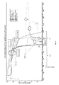
- FIG. 5 is a chart that illustrates the final boron doping profiles from the simulation testing. Referring to the x axis of the chart in FIG.
- the SiGe film width spans from 0.00 (which represents the SiGe upper surface) to 5.00, which represents the lower interface of the SiGe, which is in contact with a semiconductor substrate.
- the area to the left of 0.00 represents the contact region of the pMOSFET.
- the y axis in FIG. 5 provides the concentration of boron atoms.
- FIG. 5 includes boron doping profiles (1), not according to the invention, and (2)-(4), according to embodiments of the invention.
- FIG. 5 includes: (1) a POR constant boron doping profile, where only L 2 is boron doped (“eSiGe-POR” plot); (2) a linearly graded boron doping profile where only L 2 is boron doped (“eSiGe-L 2 -linear” plot); (3) a linearly graded boron doping profile where L 1 and L 2 are both boron-doped (“eSiGe-L 1 L 2 -linear” plot); (4) a logarithmic graded boron doping profile where only L 2 is boron doped (“eSiGe-L 2 -log” plot); and (5) a logarithmic graded boron doping profile where L 1 and L 2 are both doped (“eSiGe-L 1 -L 2 -log” plot).
- the boron-doping step for doping the SiGe films uses boron-containing gas, and the inventive embodiments of FIG. 5 have graded boron doping profiles that are achieved by controlling gas flow rate. Profiles (1)-(5) reflect final doping profiles that are obtained after all thermal budget where dopants diffuse.
- FIGS. 6A-B are charts showing Ron (resistance of device when it's on) and Cov (overlap capacitance) performance for pMOSFET's with SiGe layers having POR constant boron doping (in L 2 only), corresponding to profile (1) discussed in relation to FIG. 5 above, and logarithmic and linear doping (in L 2 only), corresponding to embodiments of the invention and to profiles (4) and (2) discussed above in relation to FIG. 5 , respectively.
- logarithmic and linear profiles (4) and (2) show better Cov performance as compared to POR (1).
- the Ron is lower for the log and linear according to embodiments of the invention, as opposed to the POR.
- the Cov is lower than for the POR.
- Ron*Cov is lowest for graded (here, log and linear) boron doping profiles as compared to that of constant boron doping used in the standard POR process.
- FIGS. 7A-E are charts showing other electrical performance comparisons as between pMOSFET's with SiGe layers having POR constant boron doping (in L 2 only), corresponding to profile (1) discussed in relation to FIG. 5 above, and logarithmic and linear doping (in L 2 only), corresponding to embodiments of the invention and to profiles (4) and (2), respectively, discussed above in relation to FIG. 5 .
- Isoff standby current
- Ieff I-effective; the effective current coming from the transistor
- Ixoff junction leakage
- Vtsat vt of transistor in saturation
- DIBL drain induced barrier lowering
- embodiments of the invention having a graded boron doping profile in L 2 demonstrate better or comparable electrical performance than the constant-boron-doped POR profile.
- FIGS. 8A-E are charts showing other electrical performance comparisons as between pMOSFET's with SiGe layers having POR constant boron doping (in L 2 only), corresponding to profile (1) discussed in relation to FIG. 5 above, and logarithmic and linear doping (in L 1 and L 2 ), corresponding to embodiments of the invention and to profiles (5) and (3), respectively, discussed above in relation to FIG. 5 .
- embodiments of the invention having a graded boron doping profile in L 1 and L 2 demonstrate better or comparable electrical performance than the constant-boron-doped POR.
- FIGS. 6A-B , 7 A-E, and 8 A-E thus demonstrate that graded boron doping of the SiGe film in accordance with the present invention results in improved overlap capacitance (Cov) without negative impact on other transistor parameters or electrical performance.
- the graded boron doping of the present invention leads to a gain on AC performance without degrading any device performance, thereby enabling better device performance by, e.g., reducing overlap capacitance and junction leakage, thus resulting on overall better chip performance.
- FIG. 9 is a chart that illustrates final boron doping profiles from simulation done using a well calibrated deck for 20 nm technology.
- the simulated profiles are based on pMOSFET's having a 50 nm thick SiGe film, where L 1 (the initially-deposited SiGe) is about 20 nm thick, and L 2 (the upper portion of the SiGe) is about 30 nm thick. Common parameters are shared for all testing, except that SiGe films have different boron doping profiles.
- the SiGe film width spans from 0.00 (which represents the SiGe upper surface) on, with L 2 spanning from 0.00 (which represents the upper surface) to 3.00.
- FIG. 9 the SiGe film width spans from 0.00 (which represents the SiGe upper surface) on, with L 2 spanning from 0.00 (which represents the upper surface) to 3.00.
- FIG. 9 includes log and linear L 2 boron doping profiles according to embodiments of the present invention, as well as an L 2 constant boron doping profile (“eSige-POR”), not according to the invention.
- FIG. 9 also includes a constant boron doping profile (also not according to the invention) that represents constant doping at three times the boron concentration used in the POR. This plot is shown as “eSiGe-POR(L 2 ⁇ 3)”.
- FIGS. 10A-C are charts showing comparative electrical parameters for a pMOSFET with SiGe film having POR constant boron doping (“por”), which corresponds to the “eSige-POR” plot from FIG. 9 , and for a pMOSFET with SiGe film that was constant boron doped, but at a boron concentration of three times that used in the POR (“por(L 2 ⁇ 3)”), which corresponds to the “eSiGe-POR(L 2 ⁇ 3)” plot from FIG. 9 .
- the charts of FIGS. 10A-C illustrate that merely increasing boron concentration degrades device performance.
- a method or device that “comprises”, “has”, “includes” or “contains” one or more steps or elements possesses those one or more steps or elements, but is not limited to possessing only those one or more steps or elements.
- a step of a method or an element of a device that “comprises”, “has”, “includes” or “contains” one or more features possesses those one or more features, but is not limited to possessing only those one or more features.
- a device or structure that is configured in a certain way is configured in at least that way, but may also be configured in ways that are not listed.
- each range is intended to be a shorthand format for presenting information, where the range is understood to encompass each discrete point within the range as if the same were fully set forth herein.
Landscapes
- Metal-Oxide And Bipolar Metal-Oxide Semiconductor Integrated Circuits (AREA)
- Insulated Gate Type Field-Effect Transistor (AREA)
Abstract
Description
-
- providing a semiconductor substrate;
- depositing a silicon-germanium (SiGe) film on the semiconductor substrate, thereby forming a lower interface of the SiGe film in contact with the semiconductor substrate, and an upper surface of the SiGe film; and
- doping the SiGe film with boron to form a SiGe film having a graded boron doping profile where boron content increases upwardly over a majority of the width of boron-doped SiGe film between the lower interface of the SiGe film and the upper surface of the SiGe film.
Claims (5)
Priority Applications (1)
| Application Number | Priority Date | Filing Date | Title |
|---|---|---|---|
| US14/259,726 US9419082B2 (en) | 2014-04-23 | 2014-04-23 | Source/drain profile engineering for enhanced p-MOSFET |
Applications Claiming Priority (1)
| Application Number | Priority Date | Filing Date | Title |
|---|---|---|---|
| US14/259,726 US9419082B2 (en) | 2014-04-23 | 2014-04-23 | Source/drain profile engineering for enhanced p-MOSFET |
Publications (2)
| Publication Number | Publication Date |
|---|---|
| US20150311293A1 US20150311293A1 (en) | 2015-10-29 |
| US9419082B2 true US9419082B2 (en) | 2016-08-16 |
Family
ID=54335531
Family Applications (1)
| Application Number | Title | Priority Date | Filing Date |
|---|---|---|---|
| US14/259,726 Expired - Fee Related US9419082B2 (en) | 2014-04-23 | 2014-04-23 | Source/drain profile engineering for enhanced p-MOSFET |
Country Status (1)
| Country | Link |
|---|---|
| US (1) | US9419082B2 (en) |
Cited By (4)
| Publication number | Priority date | Publication date | Assignee | Title |
|---|---|---|---|---|
| US11094822B1 (en) | 2020-01-24 | 2021-08-17 | Globalfoundries U.S. Inc. | Source/drain regions for transistor devices and methods of forming same |
| US11205699B2 (en) | 2019-10-17 | 2021-12-21 | Globalfoundries U.S. Inc. | Epitaxial semiconductor material regions for transistor devices and methods of forming same |
| US11239315B2 (en) | 2020-02-03 | 2022-02-01 | Globalfoundries U.S. Inc. | Dual trench isolation structures |
| US11362177B2 (en) | 2020-01-28 | 2022-06-14 | Globalfoundries U.S. Inc. | Epitaxial semiconductor material regions for transistor devices and methods of forming same |
Families Citing this family (1)
| Publication number | Priority date | Publication date | Assignee | Title |
|---|---|---|---|---|
| US11764058B2 (en) | 2021-09-28 | 2023-09-19 | Applied Materials, Inc. | Three-color 3D DRAM stack and methods of making |
Citations (6)
| Publication number | Priority date | Publication date | Assignee | Title |
|---|---|---|---|---|
| US6855963B1 (en) * | 2003-08-29 | 2005-02-15 | International Business Machines Corporation | Ultra high-speed Si/SiGe modulation-doped field effect transistors on ultra thin SOI/SGOI substrate |
| US20070235802A1 (en) * | 2006-04-05 | 2007-10-11 | Chartered Semiconductor Manufacturing Ltd | Method to control source/drain stressor profiles for stress engineering |
| US20100200937A1 (en) | 2009-02-09 | 2010-08-12 | International Business Machines Corporation | METHOD AND STRUCTURE FOR PMOS DEVICES WITH HIGH K METAL GATE INTEGRATION AND SiGe CHANNEL ENGINEERING |
| US7935612B1 (en) | 2010-02-05 | 2011-05-03 | International Business Machines Corporation | Layer transfer using boron-doped SiGe layer |
| US20120086077A1 (en) * | 2010-10-07 | 2012-04-12 | International Business Machines Corporation | Fet structures with trench implantation to improve back channel leakage and body resistance |
| US20120153399A1 (en) * | 2010-12-16 | 2012-06-21 | Globalfoundries Inc. | Low-Diffusion Drain and Source Regions in CMOS Transistors for Low Power/High Performance Applications |
-
2014
- 2014-04-23 US US14/259,726 patent/US9419082B2/en not_active Expired - Fee Related
Patent Citations (6)
| Publication number | Priority date | Publication date | Assignee | Title |
|---|---|---|---|---|
| US6855963B1 (en) * | 2003-08-29 | 2005-02-15 | International Business Machines Corporation | Ultra high-speed Si/SiGe modulation-doped field effect transistors on ultra thin SOI/SGOI substrate |
| US20070235802A1 (en) * | 2006-04-05 | 2007-10-11 | Chartered Semiconductor Manufacturing Ltd | Method to control source/drain stressor profiles for stress engineering |
| US20100200937A1 (en) | 2009-02-09 | 2010-08-12 | International Business Machines Corporation | METHOD AND STRUCTURE FOR PMOS DEVICES WITH HIGH K METAL GATE INTEGRATION AND SiGe CHANNEL ENGINEERING |
| US7935612B1 (en) | 2010-02-05 | 2011-05-03 | International Business Machines Corporation | Layer transfer using boron-doped SiGe layer |
| US20120086077A1 (en) * | 2010-10-07 | 2012-04-12 | International Business Machines Corporation | Fet structures with trench implantation to improve back channel leakage and body resistance |
| US20120153399A1 (en) * | 2010-12-16 | 2012-06-21 | Globalfoundries Inc. | Low-Diffusion Drain and Source Regions in CMOS Transistors for Low Power/High Performance Applications |
Cited By (4)
| Publication number | Priority date | Publication date | Assignee | Title |
|---|---|---|---|---|
| US11205699B2 (en) | 2019-10-17 | 2021-12-21 | Globalfoundries U.S. Inc. | Epitaxial semiconductor material regions for transistor devices and methods of forming same |
| US11094822B1 (en) | 2020-01-24 | 2021-08-17 | Globalfoundries U.S. Inc. | Source/drain regions for transistor devices and methods of forming same |
| US11362177B2 (en) | 2020-01-28 | 2022-06-14 | Globalfoundries U.S. Inc. | Epitaxial semiconductor material regions for transistor devices and methods of forming same |
| US11239315B2 (en) | 2020-02-03 | 2022-02-01 | Globalfoundries U.S. Inc. | Dual trench isolation structures |
Also Published As
| Publication number | Publication date |
|---|---|
| US20150311293A1 (en) | 2015-10-29 |
Similar Documents
| Publication | Publication Date | Title |
|---|---|---|
| US20220271125A1 (en) | Transistor devices having source/drain structure configured with high germanium content portion | |
| US9419082B2 (en) | Source/drain profile engineering for enhanced p-MOSFET | |
| US9129827B2 (en) | Conversion of strain-inducing buffer to electrical insulator | |
| US10658175B2 (en) | Semiconductor device and manufacturing method therefor | |
| US9577042B1 (en) | Semiconductor structure with multilayer III-V heterostructures | |
| US9837533B2 (en) | Semiconductor structure and manufacturing method thereof | |
| EP1965430A3 (en) | Sic semiconductor device and method for manufacturing the same | |
| TW201133834A (en) | Germanium-based quantum well devices | |
| US9673295B2 (en) | Contact resistance optimization via EPI growth engineering | |
| US9966448B2 (en) | Method of making a silicide beneath a vertical structure | |
| Yamada et al. | Suppression of surface segregation of the phosphorous δ-doping layer by insertion of an ultra-thin silicon layer for ultra-shallow Ohmic contacts on n-type germanium | |
| Hashemi et al. | First demonstration of high-Ge-content strained-Si 1− x Ge x (x= 0.5) on insulator PMOS FinFETs with high hole mobility and aggressively scaled fin dimensions and gate lengths for high-performance applications | |
| KR20110085002A (en) | Semiconductor device structure and associated method comprising a transistor having an energy barrier adjacent to the transistor channel | |
| KR102176646B1 (en) | Strain compensation in transistors | |
| US20140329374A1 (en) | Methods of fabricating quantum well field effect transistors having multiple delta doped layers | |
| Liu et al. | Demonstration of a GaN-based P-channel FinFET with high current density based on multi-channel structure | |
| CN104851783B (en) | A kind of germanium silicon boron outer layer growth method | |
| Cordier et al. | Influence of MBE growth conditions on the quality of InAlAs/InGaAs metamorphic HEMTs on GaAs | |
| CN105895668A (en) | Junction Interlayer Dielectric For Reducing Leakage Current In Semiconductor Devices | |
| Hikavyy et al. | High Ge content SiGe selective processes for source/drain in manufacturing the next generations of pMOS transistors | |
| Liow et al. | 5 nm gate length Nanowire-FETs and planar UTB-FETs with pure germanium source/drain stressors and laser-free Melt-Enhanced Dopant (MeltED) diffusion and activation technique | |
| Myronov et al. | Observation of high mobility 2DHG with very high hole density in the modulation doped strained Ge quantum well at room temperature | |
| US20070218597A1 (en) | Structure and method for controlling the behavior of dislocations in strained semiconductor layers | |
| Loo et al. | Fabrication of 50 nm high performance strained-SiGe pMOSFETs with selective epitaxial growth | |
| CN115312596B (en) | High electron mobility transistor and manufacturing method thereof |
Legal Events
| Date | Code | Title | Description |
|---|---|---|---|
| AS | Assignment |
Owner name: GLOBALFOUNDRIES INC., CAYMAN ISLANDS Free format text: ASSIGNMENT OF ASSIGNORS INTEREST;ASSIGNORS:MISHRA, SHIV KUMAR;LI, ZHIQING;BEASOR, SCOTT;AND OTHERS;REEL/FRAME:032739/0363 Effective date: 20140408 |
|
| ZAAA | Notice of allowance and fees due |
Free format text: ORIGINAL CODE: NOA |
|
| ZAAB | Notice of allowance mailed |
Free format text: ORIGINAL CODE: MN/=. |
|
| STCF | Information on status: patent grant |
Free format text: PATENTED CASE |
|
| AS | Assignment |
Owner name: WILMINGTON TRUST, NATIONAL ASSOCIATION, DELAWARE Free format text: SECURITY AGREEMENT;ASSIGNOR:GLOBALFOUNDRIES INC.;REEL/FRAME:049490/0001 Effective date: 20181127 |
|
| MAFP | Maintenance fee payment |
Free format text: PAYMENT OF MAINTENANCE FEE, 4TH YEAR, LARGE ENTITY (ORIGINAL EVENT CODE: M1551); ENTITY STATUS OF PATENT OWNER: LARGE ENTITY Year of fee payment: 4 |
|
| AS | Assignment |
Owner name: GLOBALFOUNDRIES U.S. INC., CALIFORNIA Free format text: ASSIGNMENT OF ASSIGNORS INTEREST;ASSIGNOR:GLOBALFOUNDRIES INC.;REEL/FRAME:054633/0001 Effective date: 20201022 |
|
| AS | Assignment |
Owner name: GLOBALFOUNDRIES INC., CAYMAN ISLANDS Free format text: RELEASE BY SECURED PARTY;ASSIGNOR:WILMINGTON TRUST, NATIONAL ASSOCIATION;REEL/FRAME:054636/0001 Effective date: 20201117 |
|
| AS | Assignment |
Owner name: GLOBALFOUNDRIES U.S. INC., NEW YORK Free format text: RELEASE BY SECURED PARTY;ASSIGNOR:WILMINGTON TRUST, NATIONAL ASSOCIATION;REEL/FRAME:056987/0001 Effective date: 20201117 Owner name: GLOBALFOUNDRIES U.S. INC., NEW YORK Free format text: RELEASE OF SECURITY INTEREST;ASSIGNOR:WILMINGTON TRUST, NATIONAL ASSOCIATION;REEL/FRAME:056987/0001 Effective date: 20201117 |
|
| FEPP | Fee payment procedure |
Free format text: MAINTENANCE FEE REMINDER MAILED (ORIGINAL EVENT CODE: REM.); ENTITY STATUS OF PATENT OWNER: LARGE ENTITY |
|
| LAPS | Lapse for failure to pay maintenance fees |
Free format text: PATENT EXPIRED FOR FAILURE TO PAY MAINTENANCE FEES (ORIGINAL EVENT CODE: EXP.); ENTITY STATUS OF PATENT OWNER: LARGE ENTITY |
|
| STCH | Information on status: patent discontinuation |
Free format text: PATENT EXPIRED DUE TO NONPAYMENT OF MAINTENANCE FEES UNDER 37 CFR 1.362 |
|
| FP | Lapsed due to failure to pay maintenance fee |
Effective date: 20240816 |