US9413394B1 - Digital to-analog converter system and method - Google Patents
Digital to-analog converter system and method Download PDFInfo
- Publication number
- US9413394B1 US9413394B1 US14/676,142 US201514676142A US9413394B1 US 9413394 B1 US9413394 B1 US 9413394B1 US 201514676142 A US201514676142 A US 201514676142A US 9413394 B1 US9413394 B1 US 9413394B1
- Authority
- US
- United States
- Prior art keywords
- sub
- dac
- output
- stream
- dacs
- Prior art date
- Legal status (The legal status is an assumption and is not a legal conclusion. Google has not performed a legal analysis and makes no representation as to the accuracy of the status listed.)
- Active
Links
Images


Classifications
-
- H—ELECTRICITY
- H03—ELECTRONIC CIRCUITRY
- H03M—CODING; DECODING; CODE CONVERSION IN GENERAL
- H03M1/00—Analogue/digital conversion; Digital/analogue conversion
- H03M1/66—Digital/analogue converters
- H03M1/662—Multiplexed conversion systems
-
- H—ELECTRICITY
- H03—ELECTRONIC CIRCUITRY
- H03F—AMPLIFIERS
- H03F1/00—Details of amplifiers with only discharge tubes, only semiconductor devices or only unspecified devices as amplifying elements
- H03F1/02—Modifications of amplifiers to raise the efficiency, e.g. gliding Class A stages, use of an auxiliary oscillation
-
- H—ELECTRICITY
- H03—ELECTRONIC CIRCUITRY
- H03F—AMPLIFIERS
- H03F3/00—Amplifiers with only discharge tubes or only semiconductor devices as amplifying elements
- H03F3/20—Power amplifiers, e.g. Class B amplifiers, Class C amplifiers
- H03F3/24—Power amplifiers, e.g. Class B amplifiers, Class C amplifiers of transmitter output stages
-
- H—ELECTRICITY
- H04—ELECTRIC COMMUNICATION TECHNIQUE
- H04B—TRANSMISSION
- H04B1/00—Details of transmission systems, not covered by a single one of groups H04B3/00 - H04B13/00; Details of transmission systems not characterised by the medium used for transmission
- H04B1/0003—Software-defined radio [SDR] systems, i.e. systems wherein components typically implemented in hardware, e.g. filters or modulators/demodulators, are implented using software, e.g. by involving an AD or DA conversion stage such that at least part of the signal processing is performed in the digital domain
- H04B1/0007—Software-defined radio [SDR] systems, i.e. systems wherein components typically implemented in hardware, e.g. filters or modulators/demodulators, are implented using software, e.g. by involving an AD or DA conversion stage such that at least part of the signal processing is performed in the digital domain wherein the AD/DA conversion occurs at radiofrequency or intermediate frequency stage
- H04B1/0014—Software-defined radio [SDR] systems, i.e. systems wherein components typically implemented in hardware, e.g. filters or modulators/demodulators, are implented using software, e.g. by involving an AD or DA conversion stage such that at least part of the signal processing is performed in the digital domain wherein the AD/DA conversion occurs at radiofrequency or intermediate frequency stage using DSP [Digital Signal Processor] quadrature modulation and demodulation
-
- H—ELECTRICITY
- H04—ELECTRIC COMMUNICATION TECHNIQUE
- H04B—TRANSMISSION
- H04B1/00—Details of transmission systems, not covered by a single one of groups H04B3/00 - H04B13/00; Details of transmission systems not characterised by the medium used for transmission
- H04B1/0003—Software-defined radio [SDR] systems, i.e. systems wherein components typically implemented in hardware, e.g. filters or modulators/demodulators, are implented using software, e.g. by involving an AD or DA conversion stage such that at least part of the signal processing is performed in the digital domain
- H04B1/0007—Software-defined radio [SDR] systems, i.e. systems wherein components typically implemented in hardware, e.g. filters or modulators/demodulators, are implented using software, e.g. by involving an AD or DA conversion stage such that at least part of the signal processing is performed in the digital domain wherein the AD/DA conversion occurs at radiofrequency or intermediate frequency stage
- H04B1/0025—Software-defined radio [SDR] systems, i.e. systems wherein components typically implemented in hardware, e.g. filters or modulators/demodulators, are implented using software, e.g. by involving an AD or DA conversion stage such that at least part of the signal processing is performed in the digital domain wherein the AD/DA conversion occurs at radiofrequency or intermediate frequency stage using a sampling rate lower than twice the highest frequency component of the sampled signal
-
- H—ELECTRICITY
- H04—ELECTRIC COMMUNICATION TECHNIQUE
- H04B—TRANSMISSION
- H04B1/00—Details of transmission systems, not covered by a single one of groups H04B3/00 - H04B13/00; Details of transmission systems not characterised by the medium used for transmission
- H04B1/005—Details of transmission systems, not covered by a single one of groups H04B3/00 - H04B13/00; Details of transmission systems not characterised by the medium used for transmission adapting radio receivers, transmitters andtransceivers for operation on two or more bands, i.e. frequency ranges
- H04B1/0067—Details of transmission systems, not covered by a single one of groups H04B3/00 - H04B13/00; Details of transmission systems not characterised by the medium used for transmission adapting radio receivers, transmitters andtransceivers for operation on two or more bands, i.e. frequency ranges with one or more circuit blocks in common for different bands
- H04B1/0082—Details of transmission systems, not covered by a single one of groups H04B3/00 - H04B13/00; Details of transmission systems not characterised by the medium used for transmission adapting radio receivers, transmitters andtransceivers for operation on two or more bands, i.e. frequency ranges with one or more circuit blocks in common for different bands with a common local oscillator for more than one band
-
- H—ELECTRICITY
- H04—ELECTRIC COMMUNICATION TECHNIQUE
- H04B—TRANSMISSION
- H04B1/00—Details of transmission systems, not covered by a single one of groups H04B3/00 - H04B13/00; Details of transmission systems not characterised by the medium used for transmission
- H04B1/02—Transmitters
- H04B1/04—Circuits
- H04B1/0475—Circuits with means for limiting noise, interference or distortion
-
- H—ELECTRICITY
- H03—ELECTRONIC CIRCUITRY
- H03M—CODING; DECODING; CODE CONVERSION IN GENERAL
- H03M1/00—Analogue/digital conversion; Digital/analogue conversion
- H03M1/66—Digital/analogue converters
- H03M1/74—Simultaneous conversion
- H03M1/742—Simultaneous conversion using current sources as quantisation value generators
-
- H—ELECTRICITY
- H04—ELECTRIC COMMUNICATION TECHNIQUE
- H04B—TRANSMISSION
- H04B1/00—Details of transmission systems, not covered by a single one of groups H04B3/00 - H04B13/00; Details of transmission systems not characterised by the medium used for transmission
- H04B1/02—Transmitters
- H04B1/04—Circuits
- H04B2001/0408—Circuits with power amplifiers
- H04B2001/045—Circuits with power amplifiers with means for improving efficiency
Definitions
- the present disclosure relates generally to Radio Frequency Digital-to-Analog Conversion. More particularly, the present disclosure relates to Radio Frequency Digital-to-Analog Conversion for application in cellular base stations.
- RF Radio Frequency
- 4G Long Term Evolution
- Previous-generation systems are constructed, for the most part, using classic RF system techniques, such as analog mixers and separate analog Base Band and RF filters.
- Newer systems are transitioning to make use of two new classes of circuits: RF Digital/Analog Converters (RF DACs) and RF Analog/Digital Converters (RF ADCs).
- RF DACs RF Digital/Analog Converters
- RF ADCs RF Analog/Digital Converters
- These RF converters push the Analog/Digital boundary much closer to the antenna, increasing the available RF bandwidth available and allowing for much more flexibility in the system, by pushing functionality that was previously in the analog circuits into digital circuits or even into software.
- This latter functionality is often called “Software Defined Radio”, or SDR, and is seen as the ultimate in flexibility, allowing major functional changes of the RF system through a software or firmware download.
- FIG. 1 shows a representative previous-generation signal chain; not all previous-generation signal chains would contain all the elements of FIG. 1 and there may be variants, however the differences can be readily understood.
- the signal chain accepts Base Band (BB) In-Phase/Quadrature (I/Q) sample data from the BBMedia Access Controller (MAC) through a Digital Interface 100 .
- the I/Q data (that is, the I-data and the Q-data) is interpolated to a higher sample rate through an interpolator 110 , and then is optionally modulated to adjust the center frequency to an Intermediate Frequency (IF) through a Digital Quadrature Modulator (DQM, 120 ).
- the interpolated and modulated I and Q digital signals are fed through two DACs ( 140 ) to produce an analog signal, which is filtered by two matched BB/IF filters ( 150 ).
- the filtered signal data is mixed using an Analog Quadrature Modulator (AQM, 160 ) with a Local Oscillator (LO) clock to produce an RF output.
- An RF Filter ( 170 ) filters the AQM output before amplifying it using a Power Amplifier (PA, 180 ) to produce the signal that will be actually transmitted by the antenna ( 190 ).
- PA Power Amplifier
- FIG. 1 has two clocks.
- the first the Base Band Clock (often referred to as SYSCLK), determines the sample data rate at the Digital Interface, and is also used to clock the Interpolator, DQM, and DACs.
- FIG. 1 shows all blocks running from the same clock, SYSCLK, however depending upon the details of the actual system, some other clock SYSCLK ⁇ M (M being an integer) or SYSCLK/M might actually be used in a particular block. Powers of 2 (i.e. 2 N ) are commonly used for M because they allow for ready use of efficient Digital Signal Processor (DSP) filter techniques, but other factors may also be used.
- the second clock the Local Oscillator clock (LO) drives the AQM and sets the center frequency of the transmitted RF output.
- the structure and operation of the AQM are well known to those skilled in the art.
- SYSCLK is, of necessity, a standard fixed frequency; in cellular base stations, this is typically a power of 2 multiple of 122.88 MHz or 153.6 MHz, however other frequencies may be chosen depending upon the system design.
- LO is typically the center frequency of the desired RF signal band or is slightly offset from it and, depending upon the particular frequency band being used, can vary widely from system to system. Because these two frequencies (SYSCLK and LO) are set by two different constraints, they are often completely unrelated to each other, which in turn creates challenges in frequency planning.
- Frequency planning essentially boils down to determining a pair of frequencies for SYSCLK and LO, together with an IF that when taken together create an interference-free range of frequencies for a desired RF band. Due to a number of practical circuit issues, harmonics of SYSCLK and LO will often mix together and create spurs, and if one of these spurs is in the desired RF band, performance of the RF system will be degraded.
- desired RF bands are narrow, both as a fraction of the available BB/IF bandwidth and the LO frequency, frequency planning can be straightforward.
- DPD Digital Pre-Distortion
- the required RF bandwidths are becoming much wider relative both to the BB/IF bandwidth and the LO frequency and, as a result, the frequency planning challenges are becoming harder.
- BB/IF filters are the point where the signals cross from one clock domain (SYSCLK) into the other (LO), therefore these filters, which smooth the discrete output signal generated by the DAC to make them appear to be continuous, often must have comparatively large attenuation at multiples of SYSCLK in order to attenuate images and to minimize any coupling between the two clock domains that could create spurs at the output.
- This requirement in turn requires that the BB/IF filters be of comparatively high order, which often creates significant design challenges. Some of the challenges relate to the cost (bill of materials), non-idealities, and filter design time.
- a high-order differential LC filter uses multiple high-precision components, which are expensive and occupy a large printed circuit board area. Amplitude and/or phase mismatch between the BB/IF filters introduce nonlinearities that degrade system performance. In addition, it is difficult to provide a flat filter response over a wide bandwidth. Any ripple or roll-off also degrades system response. Lastly, it is common for these radio systems to support different radio bands. It follows that the BB/IF filters will therefore need to be different for each radio band. This scales the design time as well as the number of components needed to realize the different BB/IF filters. This greatly complicates the radio system.
- IF's could be relatively large, and the signals going into the AQM were radically asymmetric in frequency.
- the BB/IF filters were truly bandpass IF filters, and every frequency band required a different filter design, which created additional challenges for RF system vendors in designing and maintaining many band-specific designs.
- RF bandwidths increased, there was a push to increase the available bandwidth from the BB portion of the system, which in turn resulted in a push to Low-IF or Zero-IF (ZIF) systems.
- ZIF Zero-IF
- FIG. 2 An example of such a signal chain is shown in FIG. 2 .
- BB I/Q samples are received from a MAC through the Digital Interface 100 .
- These signals are interpolated to a higher sample rate with the interpolator 210 , then modulated by the DQM 220 , and converted to an analog signal by the RF DAC 240 .
- the modulated signal is in turn filtered by an RF filer 270 and is then amplified by the PA 180 for transmission via the antenna 190 .
- FIG. 2 shows all blocks driven by a single clock, SYSCLK, however as with FIG. 1 , the various blocks are likely driven by multiple different clocks, all integer multiples of SYSCLK.
- the RF DAC 240 is running at a significantly higher sample rate (Fs) than the I/Q DACs 140 , the interpolator 210 and DQM 220 are similarly going to have significantly higher output sample rates than the interpolator 110 and DQM 120 .
- the first two RF DAC challenges are the so-called “sin(x)/x” or “sinc” response inherent to DAC designs and the images that come from the DAC discrete-time output.
- the output from a DAC over time is not a smooth continuous signal; it instead has a discrete-time staircase shape, sometimes called a “zero order hold”.
- the zero-order hold has a frequency response that is given by the equation sin(x)/x, which is plotted in FIG. 3 .
- the vertical axis of this figure is the frequency response in dB, while the horizontal axis is the output frequency as a fraction of Fs, which is the DAC sample rate or the DAC sampling frequency.
- the sin(x)/x response creates a frequency response notch at Fs, meaning that all signal energy at the sample rate is completely attenuated. There are additional notches at Fs ⁇ 2, Fs ⁇ 3, and so on, however these are not shown. Also shown in FIG. 3 are the first and second “Nyquist Zones”, which are frequency bands whose width is equal to the Nyquist Frequency Fs/2. Nyquist Zone 1 is a frequency band that extends from DC to Fs/2 and Nyquist Zone 2 is a frequency band that extends from Fs/2 to Fs.
- Nyquist Zone 3 extends from Fs to Fs ⁇ 3/2
- Nyquist Zone 4 extends from Fs ⁇ 3/2 to Fs ⁇ 2. Because the DAC output is a discrete-time signal, output signals that are centered on DC have images centered on Fs, Fs ⁇ 2, Fs ⁇ 3, and so on. Therefore, any signal energy in Nyquist Zone 1 will have an image (mirrored at Fs/2) in Nyquist Zone 2 and vice versa. There are additional images in all other Nyquist Zones, but for the purposes of this discussion this is not important.
- FIG. 4 shows the frequency response of two representative RF signals 401 and 402 transmitted in Nyquist Zone 1. For example, if an RF system designer wished to use the RF signal 401 , centered around Fs ⁇ 0.125, there would only be approximately 1 dB of attenuation at the center frequency of the RF signal 401 due to the sin(x)/x response, which for most systems is relatively easy to accommodate.
- FIG. 4 shows the images 411 and 412 (in Nyquist Zone 2) of the RF signals 401 and 402 (in Nyquist Zone 1). Images 411 (centered at Fs ⁇ 0.875) and 412 (centered at Fs ⁇ 0.625) are both in Nyquist Zone 2. Image 411 is approximately 16 dB attenuated relative to frequency response of the RF signal 401 , and is furthermore spaced relatively far away. As a result, the required RF filter 270 (shown in FIG. 2 ) required to reject the image 411 is relatively straight forward to construct.
- FIG. 5 shows an alternate approach, with RF signal 503 transmitted in Nyquist Zone 2 (centered at Fs ⁇ 0.75) and its image 513 in Nyquist Zone 1 (centered at Fs ⁇ 0.25).
- the image 513 is approximately 9 dB higher than the RF signal 503 , however the signal-to-image spacing is significantly greater than that of RF signal 402 to image 412 ( FIG. 4 ), which simplifies the design of the RF filter 270 .
- RF signal 503 requires a sample rate of only 5.33 Gsps, which is much lower than that required for either RF signals 401 or 402 of FIG. 4 ; however the DAC sin(x)/x response has attenuated the RF signal 503 by approximately 10 dB, meaning that approximately 90% of the signal power has been lost due to the DACs sin(x)/x response.
- RF DACs pose for the RF system designer is again frequency planning.
- the frequency planning challenges of a one-clock system arise from the fixed-frequency BB clock SYSCLK.
- the DAC's Fs is a multiple of SYSCLK which means that the system designer must choose an appropriate multiple in order to make the challenges from sin(x)/x and images manageable.
- an RF band centered around 4 GHz with a SYSCLK of 122.88 MHz and a signal placement similar to RF signal 402 FIG.
- RF Mode One approach to operating in the Nyquist zone 2 that has been used in several recent designs makes use of what is called “Mix Mode” or “RF Mode”.
- the RF DAC is configured to produce an IF signal, and then the DAC inverts its output during the second half of every sample, usually using a slight variation on the Differential Quad Switching (DQS) technique.
- DQS Differential Quad Switching
- FIG. 6 in one step this translates an IF signal 604 that was originally in Nyquist Zone 1 into an RF signal 604 A in Nyquist Zone 2 and an image 614 A of in Nyquist Zone 3, with only approximately 3 dB reduction in signal level due to sin(x)/x effects. While this technique is quite effective, it is only effective in Nyquist Zone 2 and the frequency spacing between RF signal 604 A and image 614 A must be considered (in Nyquist Zone 3) which reduces its utility somewhat.
- CMOS logic dynamic power increases linearly both with frequency and with the total capacitance being driven.
- the DQS structures are driven by arrays of digital latches, and delay mismatch between these latches appears as gain mismatch between individual LSB elements.
- LSB gain mismatch due to latch delay mismatches is the dominant source of mismatch, and in order to reduce this the devices that make up the latches are physically large, which increases the total capacitance being driven and therefore increases the power.
- Fs increases, power increases, but additionally the required latch mismatch is reduced, so the devices are made even larger, with the end result that dynamic power in the latch array tends to increase at a higher rate than just with Fs.
- the RF DAC is implemented in (Silicon CMOS, BiCMOS, or bipolar or exotic process such as SiGe, GaAs, or InP) and the minimum feature size (180 nm, 130 nm, 90 nm, 65 nm, 40 nm, 28 nm, 20 nm, or smaller) it may not even be possible to implement the chosen Fs without moving to a totally different architecture, which may increase power even more.
- the DAC sin(x)/x response, the DAC images, frequency planning, and power dissipation mean that the RF DAC transmit signal chain designer has a large design space to choose from, trading off RF DAC sample rate and architecture, RF filter complexity, and digital complexity all in order to achieve the required target specifications while overcoming all these challenges. If the RF system is intended to cover a wide range of LOs, as in a modern 4G system where LO's can potentially cover a continuous range approximately 400 MHz to 4 GHz, all the design space is much larger, because now the system must either be designed to accommodate the worst-case combination of conditions or the system must be reconfigured depending upon the LO frequency in order to remain efficient.
- the present disclosure provides a radio frequency digital-to-analog converter (DAC) system.
- the system comprises a first DAC to receive a first sample stream and to generate a first DAC output, a second DAC to receive a second sample stream and to generate a second DAC output; and a multiplexer unit to obtain the first DAC output and the second DAC output, the multiplexer unit to calculate a complementary output from the first DAC output to obtain a complementary first DAC output and a complementary output from the second DAC output to obtain a complementary second DAC output, the multiplexer to generate an interleaved output signal that contains a repeating sequence defined by: first DAC output, complementary second DAC output, complementary first DAC output, and second DAC output, the first DAC and the second DAC being clocked by a local oscillator, the repeating sequence spanning a single period of the local oscillator.
- DAC radio frequency digital-to-analog converter
- the present disclosure provides a method of effecting digital-to-analog conversion.
- the method comprises: converting a first analog sample stream into a first output, the first output being a first digital output; generating a complementary output of the first output to obtain a first complementary output; converting a second analog sample stream into a second output, the second output being a second digital output; generating a complementary output of the second output to obtain a second complementary output; multiplexing the first output, the first complementary output, the second output, and the second complementary output to obtain an interleaved signal that contains a repeating sequence defined by: first output, second complementary output, first complementary output, and second output, a conversion of the first analog sample stream and of the second analog sample stream being effected in accordance with a local oscillator, the repeating sequence spanning a single period of the local oscillator.
- FIG. 1 shows a prior art RF Transmit Signal Chain.
- FIG. 2 shows a prior art Single-Clock RF DAC Transmit Signal Chain.
- FIG. 3 is a graph showing a prior art DAC sin(x)/x Frequency Response.
- FIG. 4 is a graph showing a prior art RF DAC Images from Nyquist Zone 1.
- FIG. 5 is a graph showing prior art RF DAC Images from Nyquist Zone 2.
- FIG. 6 is a graph showing a prior art Mix-Mode RF DAC Frequency Response and Images.
- FIG. 7 is a graph showing a prior art RF DAC ‘RFZ Mode’ Frequency Response.
- FIG. 8 shows a prior art 2-Way Interleaved DAC.
- FIG. 9 shows a prior art 2-Way Interleaved DAC Timing Diagram.
- FIG. 10 is a 2-Way Interleaved DAC system in accordance with an embodiment of the present disclosure.
- FIG. 11 shows a timing diagram for the DAC system of FIG. 10 .
- FIG. 12 shows a prior art 4-Way Interleaved DAC.
- FIG. 13 shows a 4-Way Summed (Moving Average Filter) DAC system in accordance with another embodiment of the present disclosure.
- FIG. 14 is a 4-Tap and 2-Tap Moving Average Filter Responses in accordance with embodiments of the present disclosure.
- FIG. 15 shows an embodiment of a Programmable Summation DAC system in accordance with embodiments of the present disclosure.
- FIG. 16A shows an RF DAC Analog Block Diagram in accordance with embodiments of the present disclosure.
- FIG. 16B shows how a serial stream is divided into four parallel offset sub-streams.
- FIG. 17 shows an RF DAC Analog Transistor-Level Schematic in accordance with embodiments of the present disclosure.
- FIG. 18 shows an RF DAC Analog Timing Diagram in accordance with embodiments of the present disclosure.
- FIG. 19 shows a Two-Clock RF DAC Transmit Signal Chain in accordance with embodiments of the present disclosure.
- FIG. 20 is a flowchart of a method in accordance with embodiments of the present disclosure.
- the present disclosure provides a method and system for Radio Frequency Digital-to-Analog Conversion.
- Embodiments of the RF DAC architecture of the present disclosure incorporate many individual elements, both analog and digital. Many of the elements are innovative, as is the combination of elements to produce the overall RF DAC.
- the present disclosure provides an Interleaved Radio Frequency Digital-to-Analog Converter (RF DAC) suitable for use in cellular base stations and optimized to give both a wide RF tuning range and a wide RF bandwidth.
- the RF DAC uses two levels of interleaving, the first providing a direct conversion path from Base Band (BB) to RF, and the second providing a variable interleaving factor through the use of summation of DAC outputs to optimize the output bandwidth as a function of the RF center frequency.
- Digital Interpolation including an arbitrary sample rate conversion filter, allows the DAC to operate from a wide range of possible BB sample rates; the RF DAC sample rate is a fixed ratio of the RF center frequency.
- the spurious outputs from the RF DAC are at known locations that are easy to filter out, minimizing the frequency planning tasks required for a complete n RF system design.
- the RF DAC of the present disclosure is frequency-agile, power efficient, and is capable of covering an LO frequency range from at least 400 MHz to 4 GHz, with a wide RF bandwidth that is at least 800 MHz at LO frequencies greater than 1 GHz.
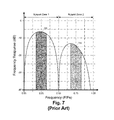
- RFZ Radio Frequency Return-to-Zero mode
- the RFZ DAC uses up-sampling to create multiple images of the real BB/IF, then uses a Finite Impulse Response discrete-time filter select the double-sided image entered around Fs ⁇ 0.25 as the desired output.
- the frequency response of such an RFZ DAC is shown in FIG. 7 , showing the modulated RF signal 705 (centered in the middle of Nyquist Zone 1, at Fs ⁇ 0.25) and the image 715 (centered at Fs ⁇ 0.75).
- the frequency response around signal 705 is quite flat, with approximately 7 dB of attenuation: 1 dB from sin(x)/x effects and 6 dB because the output is only active half the time because the RFZ DAC acts similar to a Return-to-Zero (RZ) DAC.
- the double-sided RF response is undesirable, but the flat frequency response and wide spacing from the signal to the image are both highly desirable.
- the second element of the architecture of RF DAC embodiments of the present disclosure is that it is a 2-way interleaved DAC.
- Many of the highest-speed DAC designs are constructed in two parts: a number of lower-speed Sub-DACs and an extremely high-speed analog multiplexer to time-interleave the Sub-DAC outputs together.
- a 2-way interleaved DAC shown in FIG. 8 , consists of two Sub-DACs 840 and a multiplexer 860 .
- Each Sub-DAC operates at half the desired output sample rate, for example, 8 Gsps for each Sub-DAC for an effective output sample rate of 16 Gsps.
- the timing diagram of such an interleaved DAC is shown in FIG. 9 .
- the output from Sub-DAC #0 transitions on the rising edge of the clock, while the output from Sub-DAC #1 transitions on the falling edge of the clock.
- the multiplexer 860 output is selected synchronously by the clock, and is selected during the time that the input is stable. Because the output transitions depend only on the multiplexer control input, any uncertainty on the transition times at the Sub-DAC outputs are irrelevant, which removes a major source of quantization noise in non-interleaved DACs, and in turn allows the latches that drive the Sub-DAC current steering outputs to be sized largely without consideration for mismatch. Given that the intended output sample rate is 16 Gsps (or any other suitable value) and power is an important system consideration, reducing the latch size (and power) is a significant improvement.
- the third element of the architecture of RF DAC embodiments of the present disclosure involves combining the first two elements to build a 2-way interleaved RF DAC, as is shown in FIG. 10 .
- Sub-DACs 840 are now I and Q Sub-DACs 1040 (in-phase Sub-DAC and quadrature-phase Sub-DAC), and the 2:1 multiplexer 860 is now the 4:1 multiplexer 1060 , with the two additional inputs to the multiplexer being inverted versions of the two Sub-DAC outputs.
- a multiplexer unit is a functional block that receives the Sub-DAC's outputs, generates (or calculates) a complementary output of the Sub-DAC's outputs and generates an interleaved output signal that contains a repeating sequence using the Sub-DAC's outputs or their complementary outputs.
- the I and Q Sub-DACs produce a complex BB signal, so this RF DAC structure is capable of producing a single-sided output response, unlike the double-sided output response of an RFZ DAC.
- FIG. 11 The timing diagram of such a 2-Way Interleaved RF DAC is shown in FIG. 11 . Similar to the 2-Way Interleaved DAC of FIG. 9 , inputs are selected based on the DAC clock, minimizing the effects of any timing uncertainty at the Sub-DAC outputs.
- the DAC clock has a 50% duty cycle. On alternate cycles, either the Sub-DAC outputs or their negative versions (complementary outputs) are selected, with the end result that the I Sub-DAC (as seen at the output) is effectively a full-rate signal multiplied by the sequence “1, 0, ⁇ 1, 0” while the Q Sub-DAC is similarly effectively a full-rate signal multiplied by the sequence “0, ⁇ 1, 0, 1”.
- the complex BB signal at the output from the I and Q Sub-DACs is modulated up to the RF frequency Fs/4 directly with the full-rate output signals following the sequence “I, ⁇ Q, ⁇ I, Q”.
- the 4:1 interleaving multiplexer is effectively operating as an AQM.
- the two Sub-DACs each operate similar to an RFZ DAC with 6 dB of attenuation due to their RZ nature
- the interleaving operation results in the overall RF DAC appearing as a conventional Non-Return-to-Zero (NRZ) DAC, meaning that the 6 dB attenuation due of the RZ coding is removed, leaving only the 1 dB attenuation due to sin(x)/x effects.
- NRZ Non-Return-to-Zero
- this circuit requires that I and Q sample streams be aligned so that the Q signal stream is effectively delayed by a time equal to a quarter of the LO period.
- the fourth element to the architecture is to use a programmable summation based DAC to reduce the power required to build the I and Q Sub-DACs. Even with the reduction in power that comes from reducing the sample rate from the output sample rate of 16 Gsps to the Sub-DAC sample rate of 8 Gsps, building two 8 Gsps Sub-DACs is also power-prohibitive, so these Sub-DACs are also interleaved, this time 4 ways instead of 2 ways.
- a 4-way interleaved DAC is shown in FIG. 12 . Similar to the 2-way interleaved DAC in FIG. 8 , it consists of 4 Sub-DACs 1240 and a 4:1 multiplexer 1241 , and it operates in a similar way. This reduces the DAC Fs by a factor of 4, from 8 Gsps to 2 Gsps.
- each Sub-DAC must always be active, meaning that the 4:1 multiplexer must steer the current from any un-used DAC to a low-impedance “dump” node, effectively wasting 75% of the power.
- the RF DAC structure of FIG. 10 requires that the I and Q Sub-DACs only produce low-frequency BB signals, another option, shown at FIG. 13 , is used. In the structure of FIG. 13 , the four Sub-DACs 1340 are summed together with a summation block 1341 rather than using a 4:1 multiplexer.
- a summation block can also be referred to as a summation device. This has two advantages: first, no static bias power is wasted and second, each of the Sub-DACs 1340 can be made one quarter the size of Sub-DACs 1240 saving yet more dynamic power.
- This frequency response (which can also be referred to as a transfer function) can be corrected relatively easily by adding a simple fixed DSP equalizer to implement the inverse of the MAF response (an Inverse MAF or IMAF) in the digital circuits that precede the DAC.
- a simple fixed DSP equalizer to implement the inverse of the MAF response (an Inverse MAF or IMAF) in the digital circuits that precede the DAC.
- IMAF Inverse MAF or IMAF
- a 2-tap MAF (a MAF that sums together two inputs), which has the response 1402 in FIG. 14 , and the loss due to the 2-tap MAF response across the signal band is approximately 1 dB, which again can be readily compensated for with a similar IMAF filter.
- the structure in FIG. 15 is used, which adds a set of digital multiplexers 1542 at the inputs to the Sub-DACs 1340 which allow the Sub-DACs to be driven in parallel at lower LO frequencies.
- the multiplexers 1542 that receive the I sample streams can be referred to as a switching unit and the multiplexers 1542 that receive the Q sample streams can be referred to as another switching unit.
- the four Sub-DACs are driven independently at sample rates of 1-2 Gsps and act as a 4-tap MAF.
- the four Sub-DACs are driven in pairs at 1-2 Gsps, with Sub-DACs #3 and #2 driven together and Sub-DACs #1 and #0 driven together. This effectively results in there being two Sub-DACs, each double the size (with an additional bit of resolution) compared to the 2-4 GHz case, and there being a 2-tap MAF at the output.
- This can be continued at LO frequencies less than 1 GHz where all four Sub-DACs 1340 can be driven together, acting as a single large DAC (with two additional bits of resolution) without the MAF response.
- this technique is not limited to use with four Sub-DACs; for example it is possible to drive six Sub-DAC's as either six individual Sub-DAC's with a 6-tap MAF response, three pairs with a 3-tap MAF response, two groups of three with a 2-tap MAF response, or a single large group of six.
- the I/Q Sub-DACs 1040 are constructed of the input multiplexers 1542 , the eight Sub-DACs 1340 , and the summation blocks 1341 .
- the summed outputs are combined by the 4:1 multiplexer 1060 to produce the final output.
- the output operates at a maximum sample rate of 16 Gsps, and each of the 8 Sub-DACs 1340 operates at a maximum sample rate of 2 Gsps.
- the 8 Sub-DACs 1340 are updated as 8 individual DACs, 4 pairs, or 2 quads.
- FIG. 16B shows an example of an initial serial I or Q sample stream 500 .
- This serial stream 500 is split into four parallel sub-streams streams 502 running at a lower sample rate, then each of the parallel sub-streams 502 is delayed by a different amount of time so that one sub-stream transitions every time the original serial stream transitioned. This produces four sub-streams 504 that are input into respective Sub-DACs.
- the initial serial I or Q data stream 500 is divided into two parallel offset sub-streams, and for applications where the four Sub-DACs are operating as a single larger DAC, the original serial I or Q data stream is used directly.
- the initial sample stream 500 is representable as sub-streams 504 that are interleaved with each other.
- FIG. 17 An example of a practical transistor-level implementation of the analog portions ( 1340 , 1341 , and 1060 ) is shown in FIG. 17 .
- the I/Q Sub-DACs 1340 are shown as the DQS structures 1740 .
- the detailed implementation of the DQS structures 1740 and the circuitry required to drive them is well known to those skilled in the art. Because the outputs from 1740 are current-mode, summation 1341 of FIG. 13 is performed simply by wiring the outputs in parallel, which is shown as functional block 1741 in FIG. 17 .
- the 4:1 multiplexer 1060 is shown as the array of 16 NMOS transistors 1760 , which steer the currents between the differential analog outputs OUTP/OUTN and the low-impedance DUMP node.
- the timing diagram for this circuit is shown in FIG. 18 .
- the 4:1 multiplexer inputs LO[3:0] are a set of four 25% duty cycle clocks that successively connect the I or Q Sub-DACs to OUTP/OUTN or to DUMP.
- FIG. 19 A high-level block diagram showing the complete RF DAC transmit signal chain is shown in FIG. 19 .
- FIG. 19 Comparing FIG. 19 to FIG. 1 and FIG. 2 , the design of FIG. 19 has the same digital interface 100 .
- the interpolator 1910 and DQM 1920 are similar in functionality to that of 110 and 120 , only needing to address IF modulation rather than RF modulation as in 210 and 220 .
- An additional interpolator 1930 of FIG. 19 is an arbitrary interpolator, allowing sample rate conversion between the two clocks, SYSCLK and LO.
- An additional digital delay element 1931 is inserted in one of the two paths in order to align samples to the interleaved DAC and avoid images, and the IMAF blocks 1932 are used to compensate for the MAF response of the I/Q Sub-DACs.
- the RF DAC 1940 is the 2-way interleaved RFZ structure of FIG. 16A and FIG. 17 . The output from the DAC is filtered by the RF Filter 1970 before amplification by the PA 180 for transmission over the antenna 190 .
- the individual blocks are shown as if they are driven either by SYSCLK or by LO, where in reality they will likely be driven by clocks that are related to these clocks by integer factors, and these factors are application-dependent.
- the arbitrary interpolation block 1930 is a flexible complex DSP engine, implementing a continuously-variable fractional delay filter.
- the implementation details of this block are, of necessity, well beyond the scope of this document, but it is important to note that its inclusion allows a great deal of flexibility, allowing digital control of delay and phase through the system, allowing synchronization of multiple RF DACs for Multi-Input/Multi-Output (MIMO) applications, and also allowing active compensation of I/Q delay mismatch within the RF DAC, mismatch that would result in interleaving distortion (similar to IQI and LOFT) at the output.
- the additional delay element 1931 can also be merged into 1930 as an additive delay applied to one of the paths.
- FIG. 20 shows a flowchart of a method of converting an analog signal into a digital signal, in accordance with certain embodiments of the present disclosure.
- a first analog sample stream is converted into a first output, which is digital.
- the first analog sample stream can be an in-phase sample stream or a quadrature-phase stream obtained from an initial analog signal.
- a complementary output of the first output is generated.
- a second analog sample stream is converted into a second output, which is digital.
- the second analog sample stream will be an in-phase sample stream when the first analog stream is a quadrature-phase sample stream and vice-versa.
- a complementary output of the second output is generated.
- the first output, the first complementary output, the second output, and the second complementary output are multiplexed to obtain an interleaved signal that contains a repeating sequence defined by: first output, second complementary output, first complementary output, and second output.
- the conversion of the first analog sample stream and of the second analog sample stream is effected in accordance with a local oscillator and, the repeating sequence spans a single period of the local oscillator.
- Embodiments of the disclosure or portions of such embodiments can be represented as a computer program product stored in a machine-readable medium (also referred to as a computer-readable medium, a processor-readable medium, or a computer usable medium having a computer-readable program code embodied therein).
- the machine-readable medium can be any suitable tangible, non-transitory medium, including magnetic, optical, or electrical storage medium including a diskette, compact disk read only memory (CD-ROM), memory device (volatile or non-volatile), or similar storage mechanism.
- the machine-readable medium can contain various sets of instructions, code sequences, configuration information, or other data, which, when executed, cause a processor to perform steps in a method according to an embodiment of the disclosure.
Landscapes
- Engineering & Computer Science (AREA)
- Computer Networks & Wireless Communication (AREA)
- Signal Processing (AREA)
- Power Engineering (AREA)
- Theoretical Computer Science (AREA)
- Digital Transmission Methods That Use Modulated Carrier Waves (AREA)
- Transmitters (AREA)
Abstract
Description
Claims (16)
Priority Applications (3)
| Application Number | Priority Date | Filing Date | Title |
|---|---|---|---|
| US14/676,142 US9413394B1 (en) | 2014-04-01 | 2015-04-01 | Digital to-analog converter system and method |
| US15/230,965 US9906236B2 (en) | 2014-04-01 | 2016-08-08 | Digital-to-analog converter system and method |
| US15/896,632 US10326468B2 (en) | 2014-04-01 | 2018-02-14 | Digital-to-analog converter system and method |
Applications Claiming Priority (2)
| Application Number | Priority Date | Filing Date | Title |
|---|---|---|---|
| US201461973558P | 2014-04-01 | 2014-04-01 | |
| US14/676,142 US9413394B1 (en) | 2014-04-01 | 2015-04-01 | Digital to-analog converter system and method |
Related Child Applications (1)
| Application Number | Title | Priority Date | Filing Date |
|---|---|---|---|
| US15/230,965 Continuation US9906236B2 (en) | 2014-04-01 | 2016-08-08 | Digital-to-analog converter system and method |
Publications (1)
| Publication Number | Publication Date |
|---|---|
| US9413394B1 true US9413394B1 (en) | 2016-08-09 |
Family
ID=56556029
Family Applications (3)
| Application Number | Title | Priority Date | Filing Date |
|---|---|---|---|
| US14/676,142 Active US9413394B1 (en) | 2014-04-01 | 2015-04-01 | Digital to-analog converter system and method |
| US15/230,965 Active US9906236B2 (en) | 2014-04-01 | 2016-08-08 | Digital-to-analog converter system and method |
| US15/896,632 Active US10326468B2 (en) | 2014-04-01 | 2018-02-14 | Digital-to-analog converter system and method |
Family Applications After (2)
| Application Number | Title | Priority Date | Filing Date |
|---|---|---|---|
| US15/230,965 Active US9906236B2 (en) | 2014-04-01 | 2016-08-08 | Digital-to-analog converter system and method |
| US15/896,632 Active US10326468B2 (en) | 2014-04-01 | 2018-02-14 | Digital-to-analog converter system and method |
Country Status (1)
| Country | Link |
|---|---|
| US (3) | US9413394B1 (en) |
Cited By (17)
| Publication number | Priority date | Publication date | Assignee | Title |
|---|---|---|---|---|
| US20180191369A1 (en) * | 2015-08-27 | 2018-07-05 | Nippon Telegraph And Telephone Corporation | Signal generating device |
| US20180197618A1 (en) * | 2017-01-10 | 2018-07-12 | Thales | Sample-and-hold circuit for an electrical signal |
| WO2018132230A1 (en) | 2017-01-12 | 2018-07-19 | Jariet Technologies, Inc. | Current steering digital-to-analog conversion systems |
| US10587354B1 (en) * | 2018-11-26 | 2020-03-10 | Intel Corporation | Multiphase transmitter digital front end |
| US10644716B1 (en) | 2019-08-26 | 2020-05-05 | Analog Devices International Unlimited Company | Multi-path dual-switch digital-to-analog converter |
| US10700902B1 (en) | 2019-03-14 | 2020-06-30 | Intel Corporation | Modifying a sampling frequency in a radio frequency digital to analog converter |
| US10951226B2 (en) * | 2018-12-27 | 2021-03-16 | Texas Instruments Incorporated | Radio-frequency digital-to-analog converter system |
| EP3649736A4 (en) * | 2017-07-05 | 2021-03-24 | Jariet Technologies, Inc. | ULTRA-HIGH-SPEED DIGITAL-ANALOGUE CONVERSION (DAC) METHODS AND APPARATUS WITH SUB-DAC SYSTEMS FOR DATA INTERLACING AND NON-INTERLACING POWER COMBINATOR |
| US11171674B2 (en) * | 2019-09-18 | 2021-11-09 | Texas Instruments Incorporated | Low-complexity inverse sinc for RF sampling transmitters |
| US20220006465A1 (en) * | 2019-03-14 | 2022-01-06 | Mixed-Signal Devices Inc. | Linearization of Digital-to-Analog Converters (DACs) and Analog-to-Digital Converters (ADCs) and Associated Methods |
| US20220239304A1 (en) * | 2021-01-27 | 2022-07-28 | Texas Instruments Incorporated | Fdac/2 spur estimation and correction |
| US11481679B2 (en) * | 2020-03-02 | 2022-10-25 | Kyndryl, Inc. | Adaptive data ingestion rates |
| US20230097708A1 (en) * | 2021-09-22 | 2023-03-30 | Qualcomm Incorporated | Return-to-zero (rz) digital-to-analog converter (dac) for image cancellation |
| US20230208429A1 (en) * | 2021-12-23 | 2023-06-29 | Intel Corporation | System and method for calibrating a time-interleaved digital-to-analog converter |
| WO2024137089A1 (en) * | 2022-12-20 | 2024-06-27 | Qualcomm Incorporated | Reconfigurable transmit digital-to-analog converter (dac) circuit |
| US12123968B2 (en) | 2021-02-05 | 2024-10-22 | Mixed-Signal Devices Inc. | Systems and methods for digital signal chirp generation using frequency multipliers |
| US20250253861A1 (en) * | 2024-02-05 | 2025-08-07 | Huawei Technologies Co., Ltd. | Systems and methods for data signal multiplexing |
Families Citing this family (7)
| Publication number | Priority date | Publication date | Assignee | Title |
|---|---|---|---|---|
| US10241538B2 (en) * | 2017-02-22 | 2019-03-26 | Integrated Device Technology, Inc. | Resynchronization of a clock associated with each data bit in a double data rate memory system |
| NL2018990B1 (en) * | 2017-05-30 | 2018-12-07 | Univ Delft Tech | Digitally-intensive transmitter having wideband, linear, direct-digital rf modulator |
| US10680636B2 (en) | 2018-03-26 | 2020-06-09 | Samsung Electronics Co., Ltd. | Analog-to-digital converter (ADC) with reset skipping operation and analog-to-digital conversion method |
| US10305504B1 (en) * | 2018-04-17 | 2019-05-28 | MACOM Technology Solutions Holding, Inc. | High frequency digital-to-analog conversion by interleaving without return-to-zero |
| US10374623B1 (en) * | 2018-06-11 | 2019-08-06 | Ciena Corporation | Digital-to-analog converter and generation of high-bandwidth analog signals |
| US12399523B2 (en) * | 2023-01-19 | 2025-08-26 | Apple Inc. | Wireless circuitry with time aligned data streams |
| US12512849B1 (en) | 2024-07-01 | 2025-12-30 | Bae Systems Information And Electronic Systems Integration Inc. | Direct digital synthesis circuit with multiple digital to analog converters and multi-mode mixer |
Citations (22)
| Publication number | Priority date | Publication date | Assignee | Title |
|---|---|---|---|---|
| US4591832A (en) * | 1984-07-18 | 1986-05-27 | Rca Corporation | Digital-to-analog conversion system as for use in a digital TV receiver |
| US20030020644A1 (en) * | 1998-12-21 | 2003-01-30 | Yeap Tet Hin | High speed digital-to -analog converter |
| US7221300B2 (en) | 2004-05-21 | 2007-05-22 | Texas Instruments Incorporated | Digital-to-analog converter data rate reduction by interleaving and recombination through mixer switching |
| US20070237259A1 (en) * | 2006-04-07 | 2007-10-11 | Hon Hai Precision Industry Co., Ltd. | Circuit for canceling dc offset in a communication system |
| US7583117B2 (en) * | 2006-04-20 | 2009-09-01 | Realtek Semiconductor Corp. | Delay lock clock synthesizer and method thereof |
| US20110074613A1 (en) * | 2009-09-25 | 2011-03-31 | Freescale Semiconductor, Inc. | Multiple-bit, digital-to-analog converters and conversion methods |
| US20110097091A1 (en) * | 2008-06-30 | 2011-04-28 | Huawei Technologies Co., Ltd. | Time delay adjustment device and method |
| US20110299207A1 (en) | 2010-06-04 | 2011-12-08 | Maxim Integrated Products, Inc. | High speed digital-to-analog converter with low voltage device protection |
| US20110304489A1 (en) * | 2010-06-15 | 2011-12-15 | Zoran Corporation | Methods of and arrangements for offset compensation of an analog-to-digital converter |
| US20120195352A1 (en) * | 2011-02-02 | 2012-08-02 | Rf Micro Devices, Inc. | Fast envelope system calibration |
| US20120269293A1 (en) * | 2011-04-21 | 2012-10-25 | Chun-Hsien Peng | Rf transmitter architecture, integrated circuit device, wireless communication unit and method therefor |
| US20120288018A1 (en) * | 2011-05-09 | 2012-11-15 | Saleh Osman | Efficient cartesian transmitter using signal combiner |
| US20130120190A1 (en) * | 2011-11-14 | 2013-05-16 | Earl W. McCune, Jr. | Phased array transmission methods and apparatus |
| US8548071B2 (en) * | 2011-07-19 | 2013-10-01 | Xilinx, Inc. | Integrated circuit enabling the communication of data and a method of communicating data in an integrated circuit |
| US20130272441A1 (en) * | 2011-01-12 | 2013-10-17 | Adc Telecommunications, Inc. | Distinct transport path for mimo transmissions in distributed antenna systems |
| US20140079098A1 (en) * | 2012-04-09 | 2014-03-20 | Regents Of The University Of Minnesota | Multi-stage charge re-use analog circuits |
| US20140170997A1 (en) * | 2012-12-19 | 2014-06-19 | Mstar Semiconductor, Inc. | Power amplifying apparatus and wireless signal transmitter utilizing the same |
| US8805296B2 (en) * | 2012-01-26 | 2014-08-12 | Lime Microsystems Limited | Field programmable transceiver circuits |
| US20140286360A1 (en) * | 2003-06-10 | 2014-09-25 | Shared Spectrum Company | Method and system for transmitting signals with reduced spurious emissions |
| US20140314184A1 (en) * | 2013-04-23 | 2014-10-23 | Mediatek Inc. | Wireless transmitter for multi-mode concurrent transmission of signals complying with different communication standards |
| US20150050030A1 (en) * | 2012-03-22 | 2015-02-19 | Nec Corporation | Optical transmitter and method for controlling the same |
| US9093955B2 (en) * | 2013-03-21 | 2015-07-28 | Tektronix, Inc. | Asynchronous time-interleaved waveform generator using harmonic mixing |
Family Cites Families (19)
| Publication number | Priority date | Publication date | Assignee | Title |
|---|---|---|---|---|
| US5155386A (en) * | 1991-06-03 | 1992-10-13 | Motorola, Inc. | Programmable hysteresis comparator |
| JP2001308804A (en) * | 2000-04-27 | 2001-11-02 | Agilent Technologies Japan Ltd | Interleaving method having redundancy, a/d converter and d/a converter utilizing the same, and track hold circuit |
| JP3703083B2 (en) * | 2001-01-10 | 2005-10-05 | 松下電器産業株式会社 | Waveform generator |
| KR100760935B1 (en) * | 2001-02-19 | 2007-09-21 | 엘지.필립스 엘시디 주식회사 | Data driving circuit of liquid crystal display device |
| US6822595B1 (en) * | 2003-06-18 | 2004-11-23 | Northrop Grumman Corporation | Extended range digital-to-analog conversion |
| US8391322B2 (en) * | 2003-07-09 | 2013-03-05 | Broadcom Corporation | Method and system for single weight (SW) antenna system for spatial multiplexing (SM) MIMO system for WCDMA/HSDPA |
| KR20050123487A (en) * | 2004-06-25 | 2005-12-29 | 엘지.필립스 엘시디 주식회사 | The liquid crystal display device and the method for driving the same |
| US8102954B2 (en) * | 2005-04-26 | 2012-01-24 | Mks Instruments, Inc. | Frequency interference detection and correction |
| US8565345B2 (en) * | 2005-10-04 | 2013-10-22 | Hypres Inc. | Oversampling digital radio frequency transmitter |
| TWI330000B (en) * | 2006-07-27 | 2010-09-01 | Realtek Semiconductor Corp | A calibration apparatus for mismatches of time-interleaved analog-to-digital converter |
| US7446688B1 (en) * | 2007-05-09 | 2008-11-04 | Windond Electronics Corporation | Sequence generation for mismatch-shaping circuits |
| US7538704B2 (en) * | 2007-06-19 | 2009-05-26 | Telefonaktiebolaget Lm Ericsson (Publ) | Direct RF D-to-A conversion |
| WO2009008445A1 (en) * | 2007-07-10 | 2009-01-15 | Nec Corporation | Signal processor and signal processing method |
| US20100073206A1 (en) * | 2008-09-24 | 2010-03-25 | Mediatek Inc. | Analog-to-digital conversion circuits and method for calibrating thereof |
| TW201123724A (en) * | 2009-12-31 | 2011-07-01 | Sunplus Technology Co Ltd | Detector for detecting connection of video signal applied to multi-media apparatus |
| US8477058B2 (en) * | 2011-10-12 | 2013-07-02 | Ncku Research And Development Foundation | Successive approximation analog to digital converter with a direct switching technique for capacitor array through comparator output and method thereof |
| TWI443625B (en) * | 2011-11-18 | 2014-07-01 | Au Optronics Corp | Display panel and method for driving display panel |
| US8823568B2 (en) * | 2012-09-28 | 2014-09-02 | Intel Corporation | Methods and arrangements for high-speed digital-to-analog conversion |
| US9330618B2 (en) * | 2013-04-12 | 2016-05-03 | Lg Display Co., Ltd. | Driving circuit for display device and method of driving the same |
-
2015
- 2015-04-01 US US14/676,142 patent/US9413394B1/en active Active
-
2016
- 2016-08-08 US US15/230,965 patent/US9906236B2/en active Active
-
2018
- 2018-02-14 US US15/896,632 patent/US10326468B2/en active Active
Patent Citations (23)
| Publication number | Priority date | Publication date | Assignee | Title |
|---|---|---|---|---|
| US4591832A (en) * | 1984-07-18 | 1986-05-27 | Rca Corporation | Digital-to-analog conversion system as for use in a digital TV receiver |
| US20030020644A1 (en) * | 1998-12-21 | 2003-01-30 | Yeap Tet Hin | High speed digital-to -analog converter |
| US20140286360A1 (en) * | 2003-06-10 | 2014-09-25 | Shared Spectrum Company | Method and system for transmitting signals with reduced spurious emissions |
| US7221300B2 (en) | 2004-05-21 | 2007-05-22 | Texas Instruments Incorporated | Digital-to-analog converter data rate reduction by interleaving and recombination through mixer switching |
| US20070237259A1 (en) * | 2006-04-07 | 2007-10-11 | Hon Hai Precision Industry Co., Ltd. | Circuit for canceling dc offset in a communication system |
| US7583117B2 (en) * | 2006-04-20 | 2009-09-01 | Realtek Semiconductor Corp. | Delay lock clock synthesizer and method thereof |
| US20110097091A1 (en) * | 2008-06-30 | 2011-04-28 | Huawei Technologies Co., Ltd. | Time delay adjustment device and method |
| US20110074613A1 (en) * | 2009-09-25 | 2011-03-31 | Freescale Semiconductor, Inc. | Multiple-bit, digital-to-analog converters and conversion methods |
| US8022850B2 (en) * | 2009-09-25 | 2011-09-20 | Freescale Semiconductor, Inc. | Multiple-bit, digital-to-analog converters and conversion methods |
| US20110299207A1 (en) | 2010-06-04 | 2011-12-08 | Maxim Integrated Products, Inc. | High speed digital-to-analog converter with low voltage device protection |
| US20110304489A1 (en) * | 2010-06-15 | 2011-12-15 | Zoran Corporation | Methods of and arrangements for offset compensation of an analog-to-digital converter |
| US20130272441A1 (en) * | 2011-01-12 | 2013-10-17 | Adc Telecommunications, Inc. | Distinct transport path for mimo transmissions in distributed antenna systems |
| US20120195352A1 (en) * | 2011-02-02 | 2012-08-02 | Rf Micro Devices, Inc. | Fast envelope system calibration |
| US20120269293A1 (en) * | 2011-04-21 | 2012-10-25 | Chun-Hsien Peng | Rf transmitter architecture, integrated circuit device, wireless communication unit and method therefor |
| US20120288018A1 (en) * | 2011-05-09 | 2012-11-15 | Saleh Osman | Efficient cartesian transmitter using signal combiner |
| US8548071B2 (en) * | 2011-07-19 | 2013-10-01 | Xilinx, Inc. | Integrated circuit enabling the communication of data and a method of communicating data in an integrated circuit |
| US20130120190A1 (en) * | 2011-11-14 | 2013-05-16 | Earl W. McCune, Jr. | Phased array transmission methods and apparatus |
| US8805296B2 (en) * | 2012-01-26 | 2014-08-12 | Lime Microsystems Limited | Field programmable transceiver circuits |
| US20150050030A1 (en) * | 2012-03-22 | 2015-02-19 | Nec Corporation | Optical transmitter and method for controlling the same |
| US20140079098A1 (en) * | 2012-04-09 | 2014-03-20 | Regents Of The University Of Minnesota | Multi-stage charge re-use analog circuits |
| US20140170997A1 (en) * | 2012-12-19 | 2014-06-19 | Mstar Semiconductor, Inc. | Power amplifying apparatus and wireless signal transmitter utilizing the same |
| US9093955B2 (en) * | 2013-03-21 | 2015-07-28 | Tektronix, Inc. | Asynchronous time-interleaved waveform generator using harmonic mixing |
| US20140314184A1 (en) * | 2013-04-23 | 2014-10-23 | Mediatek Inc. | Wireless transmitter for multi-mode concurrent transmission of signals complying with different communication standards |
Cited By (30)
| Publication number | Priority date | Publication date | Assignee | Title |
|---|---|---|---|---|
| US10177780B2 (en) * | 2015-08-27 | 2019-01-08 | Nippon Telegraph And Telephone Corporation | Signal generating device |
| US20180191369A1 (en) * | 2015-08-27 | 2018-07-05 | Nippon Telegraph And Telephone Corporation | Signal generating device |
| US20180197618A1 (en) * | 2017-01-10 | 2018-07-12 | Thales | Sample-and-hold circuit for an electrical signal |
| US10276255B2 (en) * | 2017-01-10 | 2019-04-30 | Thales | Sample-and-hold circuit for an electrical signal |
| EP3568917A4 (en) * | 2017-01-12 | 2020-11-04 | Jariet Technologies, Inc. | FLOW CONTROLLING DIGITAL-ANALOG CONVERSION SYSTEMS |
| WO2018132230A1 (en) | 2017-01-12 | 2018-07-19 | Jariet Technologies, Inc. | Current steering digital-to-analog conversion systems |
| US11005494B2 (en) | 2017-01-12 | 2021-05-11 | Jariet Technologies, Inc. | Current steering digital-to-analog conversion systems |
| EP3649736A4 (en) * | 2017-07-05 | 2021-03-24 | Jariet Technologies, Inc. | ULTRA-HIGH-SPEED DIGITAL-ANALOGUE CONVERSION (DAC) METHODS AND APPARATUS WITH SUB-DAC SYSTEMS FOR DATA INTERLACING AND NON-INTERLACING POWER COMBINATOR |
| US10587354B1 (en) * | 2018-11-26 | 2020-03-10 | Intel Corporation | Multiphase transmitter digital front end |
| US10951226B2 (en) * | 2018-12-27 | 2021-03-16 | Texas Instruments Incorporated | Radio-frequency digital-to-analog converter system |
| US11509325B2 (en) | 2018-12-27 | 2022-11-22 | Texas Instruments Incorporated | Radio-frequency digital-to-analog converter system |
| US10700902B1 (en) | 2019-03-14 | 2020-06-30 | Intel Corporation | Modifying a sampling frequency in a radio frequency digital to analog converter |
| US20220006465A1 (en) * | 2019-03-14 | 2022-01-06 | Mixed-Signal Devices Inc. | Linearization of Digital-to-Analog Converters (DACs) and Analog-to-Digital Converters (ADCs) and Associated Methods |
| US12206425B2 (en) * | 2019-03-14 | 2025-01-21 | Mixed-Signal Devices Inc. | Linearization of digital-to-analog converters (DACs) and analog-to-digital converters (ADCs) and associated methods |
| US20240063803A1 (en) * | 2019-03-14 | 2024-02-22 | Mixed-Signal Devices Inc. | Linearization of Digital-to-Analog Converters (DACs) and Analog-to-Digital Converters (ADCs) and Associated Methods |
| US11777511B2 (en) * | 2019-03-14 | 2023-10-03 | Mixed-Signal Devices Inc. | Linearization of digital-to-analog converters (DACs) and analog-to-digital converters (ADCs) and associated methods |
| US10644716B1 (en) | 2019-08-26 | 2020-05-05 | Analog Devices International Unlimited Company | Multi-path dual-switch digital-to-analog converter |
| US11171674B2 (en) * | 2019-09-18 | 2021-11-09 | Texas Instruments Incorporated | Low-complexity inverse sinc for RF sampling transmitters |
| US11757475B2 (en) | 2019-09-18 | 2023-09-12 | Texas Instruments Incorporated | Low-complexity inverse sinc for RF sampling transmitters |
| US11481679B2 (en) * | 2020-03-02 | 2022-10-25 | Kyndryl, Inc. | Adaptive data ingestion rates |
| US20220239304A1 (en) * | 2021-01-27 | 2022-07-28 | Texas Instruments Incorporated | Fdac/2 spur estimation and correction |
| US11777513B2 (en) * | 2021-01-27 | 2023-10-03 | Texas Instruments Incorporated | FDAC/2 spur estimation and correction |
| US12123968B2 (en) | 2021-02-05 | 2024-10-22 | Mixed-Signal Devices Inc. | Systems and methods for digital signal chirp generation using frequency multipliers |
| US11621716B1 (en) * | 2021-09-22 | 2023-04-04 | Qualcomm Incorporated | Return-to-zero (RZ) digital-to-analog converter (DAC) for image cancellation |
| US20230097708A1 (en) * | 2021-09-22 | 2023-03-30 | Qualcomm Incorporated | Return-to-zero (rz) digital-to-analog converter (dac) for image cancellation |
| US20230208429A1 (en) * | 2021-12-23 | 2023-06-29 | Intel Corporation | System and method for calibrating a time-interleaved digital-to-analog converter |
| US12407357B2 (en) * | 2021-12-23 | 2025-09-02 | Intel Corporation | System and method for calibrating a time-interleaved digital-to-analog converter |
| WO2024137089A1 (en) * | 2022-12-20 | 2024-06-27 | Qualcomm Incorporated | Reconfigurable transmit digital-to-analog converter (dac) circuit |
| US12381571B2 (en) | 2022-12-20 | 2025-08-05 | Qualcomm Incorporated | Reconfigurable transmit digital-to-analog converter (DAC) circuit |
| US20250253861A1 (en) * | 2024-02-05 | 2025-08-07 | Huawei Technologies Co., Ltd. | Systems and methods for data signal multiplexing |
Also Published As
| Publication number | Publication date |
|---|---|
| US20180191368A1 (en) | 2018-07-05 |
| US10326468B2 (en) | 2019-06-18 |
| US20170134037A1 (en) | 2017-05-11 |
| US9906236B2 (en) | 2018-02-27 |
Similar Documents
| Publication | Publication Date | Title |
|---|---|---|
| US10326468B2 (en) | Digital-to-analog converter system and method | |
| Luschas et al. | Radio frequency digital-to-analog converter | |
| US7528754B1 (en) | Finite impulse response digital to analog converter | |
| US7852249B2 (en) | Sigma-delta modulator with digitally filtered delay compensation | |
| JP5510464B2 (en) | Continuous-time sigma-delta modulator with multiple feedback paths with independent delays | |
| Eloranta et al. | A Multimode Transmitter in 0.13$\mu\hbox {m} $ CMOS Using Direct-Digital RF Modulator | |
| US8063806B2 (en) | Apparatus comprising frequency selective circuit and method | |
| US20140269988A1 (en) | Radio frequency domain digital pre-distortion | |
| TWI596891B (en) | Hybrid digital/analog power amplifier | |
| US8542773B2 (en) | Digital RF converter, digital RF modulator and transmitter including the same | |
| KR101696269B1 (en) | Delta-sigma modulator and transmitter having the same | |
| CN106341134B (en) | Digital-to-analog converter with local interleaving and resampling | |
| US7312737B2 (en) | Bandwidth enhancement by time interleaving multiple digital to analog converters | |
| NL2018990B1 (en) | Digitally-intensive transmitter having wideband, linear, direct-digital rf modulator | |
| Jain et al. | Continuous-time delta-sigma modulators with time-interleaved FIR feedback | |
| US8773296B1 (en) | Interleaved digital to analog conversion | |
| Gebreyohannes et al. | All-digital transmitter architecture based on two-path parallel 1-bit high pass filtering DACs | |
| Balasubramanian et al. | Architectural trends in GHz speed DACs | |
| Van Zeijl et al. | On the attenuation of DAC aliases through multiphase clocking | |
| US8659458B1 (en) | Multiple return-to-zero current switching digital-to-analog converter for RF signal generation | |
| KR101292667B1 (en) | Digital RF converter and digital RF modulator and transmitter including the same | |
| Seddighrad et al. | A 3.6 GHz, 16mW ΣΔ DAC for a 802.11 n/802.16 e transmitter with 30dB digital power control in 90nm CMOS | |
| Jerng | Delta-Sigma digital-RF modulation for high data rate transmitters | |
| US10686476B1 (en) | Digital RF-DAC | |
| US10708113B2 (en) | Digital power amplification circuit |
Legal Events
| Date | Code | Title | Description |
|---|---|---|---|
| AS | Assignment |
Owner name: PMC-SIERRA US, INC., CALIFORNIA Free format text: ASSIGNMENT OF ASSIGNORS INTEREST;ASSIGNOR:LYE, WILLIAM MICHAEL;REEL/FRAME:036325/0404 Effective date: 20150330 Owner name: PMC-SIERRA US, INC., CALIFORNIA Free format text: ASSIGNMENT OF ASSIGNORS INTEREST;ASSIGNOR:GROE, JOHN B.;REEL/FRAME:036357/0637 Effective date: 20150404 |
|
| AS | Assignment |
Owner name: MORGAN STANLEY SENIOR FUNDING, INC., NEW YORK Free format text: PATENT SECURITY AGREEMENT;ASSIGNORS:MICROSEMI STORAGE SOLUTIONS, INC. (F/K/A PMC-SIERRA, INC.);MICROSEMI STORAGE SOLUTIONS (U.S.), INC. (F/K/A PMC-SIERRA US, INC.);REEL/FRAME:037689/0719 Effective date: 20160115 |
|
| AS | Assignment |
Owner name: MICROSEMI STORAGE SOLUTIONS (U.S.), INC., CALIFORN Free format text: CHANGE OF NAME;ASSIGNOR:PMC-SIERRA US, INC.;REEL/FRAME:038213/0291 Effective date: 20160115 |
|
| AS | Assignment |
Owner name: MICROSEMI STORAGE SOLUTIONS, INC. (FORMERLY KNOW A Free format text: PARTIAL RELEASE OF SECURITY INTEREST IN PATENTS;ASSIGNOR:MORGAN STANLEY SENIOR FUNDING, INC.;REEL/FRAME:038557/0236 Effective date: 20160428 Owner name: MICROSEMI STORAGE SOLUTIONS (U.S.), INC. (FORMERLY Free format text: PARTIAL RELEASE OF SECURITY INTEREST IN PATENTS;ASSIGNOR:MORGAN STANLEY SENIOR FUNDING, INC.;REEL/FRAME:038557/0236 Effective date: 20160428 |
|
| STCF | Information on status: patent grant |
Free format text: PATENTED CASE |
|
| AS | Assignment |
Owner name: MAXLINEAR ASIA SINGAPORE PTE LTD., SINGAPORE Free format text: ASSIGNMENT OF ASSIGNORS INTEREST;ASSIGNOR:MICROSEMI STORAGE SOLUTIONS, INC.;REEL/FRAME:039463/0743 Effective date: 20160427 |
|
| AS | Assignment |
Owner name: MICROSEMI STORAGE SOLUTIONS, INC., CALIFORNIA Free format text: ASSIGNMENT OF ASSIGNORS INTEREST;ASSIGNOR:MICROSEMI STORAGE SOLUTIONS (U.S.), INC.;REEL/FRAME:040045/0938 Effective date: 20161013 |
|
| AS | Assignment |
Owner name: MICROSEMI STORAGE SOLUTIONS, INC., CALIFORNIA Free format text: RELEASE BY SECURED PARTY;ASSIGNOR:MORGAN STANLEY SENIOR FUNDING, INC.;REEL/FRAME:046251/0271 Effective date: 20180529 Owner name: MICROSEMI STORAGE SOLUTIONS (U.S.), INC., CALIFORN Free format text: RELEASE BY SECURED PARTY;ASSIGNOR:MORGAN STANLEY SENIOR FUNDING, INC.;REEL/FRAME:046251/0271 Effective date: 20180529 |
|
| MAFP | Maintenance fee payment |
Free format text: PAYMENT OF MAINTENANCE FEE, 4TH YEAR, LARGE ENTITY (ORIGINAL EVENT CODE: M1551); ENTITY STATUS OF PATENT OWNER: LARGE ENTITY Year of fee payment: 4 |
|
| MAFP | Maintenance fee payment |
Free format text: PAYMENT OF MAINTENANCE FEE, 8TH YEAR, LARGE ENTITY (ORIGINAL EVENT CODE: M1552); ENTITY STATUS OF PATENT OWNER: LARGE ENTITY Year of fee payment: 8 |