US9390934B2 - Phase shift mask, method of forming asymmetric pattern, method of manufacturing diffraction grating, and method of manufacturing semiconductor device - Google Patents
Phase shift mask, method of forming asymmetric pattern, method of manufacturing diffraction grating, and method of manufacturing semiconductor device Download PDFInfo
- Publication number
- US9390934B2 US9390934B2 US14/350,314 US201214350314A US9390934B2 US 9390934 B2 US9390934 B2 US 9390934B2 US 201214350314 A US201214350314 A US 201214350314A US 9390934 B2 US9390934 B2 US 9390934B2
- Authority
- US
- United States
- Prior art keywords
- phase shift
- light
- shift mask
- transmission part
- diffraction grating
- Prior art date
- Legal status (The legal status is an assumption and is not a legal conclusion. Google has not performed a legal analysis and makes no representation as to the accuracy of the status listed.)
- Expired - Fee Related, expires
Links
Images


Classifications
-
- H01L21/3065—
-
- H—ELECTRICITY
- H10—SEMICONDUCTOR DEVICES; ELECTRIC SOLID-STATE DEVICES NOT OTHERWISE PROVIDED FOR
- H10P—GENERIC PROCESSES OR APPARATUS FOR THE MANUFACTURE OR TREATMENT OF DEVICES COVERED BY CLASS H10
- H10P50/00—Etching of wafers, substrates or parts of devices
- H10P50/20—Dry etching; Plasma etching; Reactive-ion etching
- H10P50/24—Dry etching; Plasma etching; Reactive-ion etching of semiconductor materials
- H10P50/242—Dry etching; Plasma etching; Reactive-ion etching of semiconductor materials of Group IV materials
-
- G03F1/0046—
-
- G—PHYSICS
- G03—PHOTOGRAPHY; CINEMATOGRAPHY; ANALOGOUS TECHNIQUES USING WAVES OTHER THAN OPTICAL WAVES; ELECTROGRAPHY; HOLOGRAPHY
- G03F—PHOTOMECHANICAL PRODUCTION OF TEXTURED OR PATTERNED SURFACES, e.g. FOR PRINTING, FOR PROCESSING OF SEMICONDUCTOR DEVICES; MATERIALS THEREFOR; ORIGINALS THEREFOR; APPARATUS SPECIALLY ADAPTED THEREFOR
- G03F1/00—Originals for photomechanical production of textured or patterned surfaces, e.g., masks, photo-masks, reticles; Mask blanks or pellicles therefor; Containers specially adapted therefor; Preparation thereof
- G03F1/26—Phase shift masks [PSM]; PSM blanks; Preparation thereof
- G03F1/28—Phase shift masks [PSM]; PSM blanks; Preparation thereof with three or more diverse phases on the same PSM; Preparation thereof
-
- G—PHYSICS
- G03—PHOTOGRAPHY; CINEMATOGRAPHY; ANALOGOUS TECHNIQUES USING WAVES OTHER THAN OPTICAL WAVES; ELECTROGRAPHY; HOLOGRAPHY
- G03F—PHOTOMECHANICAL PRODUCTION OF TEXTURED OR PATTERNED SURFACES, e.g. FOR PRINTING, FOR PROCESSING OF SEMICONDUCTOR DEVICES; MATERIALS THEREFOR; ORIGINALS THEREFOR; APPARATUS SPECIALLY ADAPTED THEREFOR
- G03F1/00—Originals for photomechanical production of textured or patterned surfaces, e.g., masks, photo-masks, reticles; Mask blanks or pellicles therefor; Containers specially adapted therefor; Preparation thereof
- G03F1/26—Phase shift masks [PSM]; PSM blanks; Preparation thereof
- G03F1/30—Alternating PSM, e.g. Levenson-Shibuya PSM; Preparation thereof
-
- H01L21/3085—
-
- H—ELECTRICITY
- H10—SEMICONDUCTOR DEVICES; ELECTRIC SOLID-STATE DEVICES NOT OTHERWISE PROVIDED FOR
- H10P—GENERIC PROCESSES OR APPARATUS FOR THE MANUFACTURE OR TREATMENT OF DEVICES COVERED BY CLASS H10
- H10P50/00—Etching of wafers, substrates or parts of devices
- H10P50/69—Etching of wafers, substrates or parts of devices using masks for semiconductor materials
- H10P50/691—Etching of wafers, substrates or parts of devices using masks for semiconductor materials for Group V materials or Group III-V materials
- H10P50/693—Etching of wafers, substrates or parts of devices using masks for semiconductor materials for Group V materials or Group III-V materials characterised by their size, orientation, disposition, behaviour or shape, in horizontal or vertical plane
- H10P50/694—Etching of wafers, substrates or parts of devices using masks for semiconductor materials for Group V materials or Group III-V materials characterised by their size, orientation, disposition, behaviour or shape, in horizontal or vertical plane characterised by their behaviour during the process, e.g. soluble masks or redeposited masks
-
- G—PHYSICS
- G03—PHOTOGRAPHY; CINEMATOGRAPHY; ANALOGOUS TECHNIQUES USING WAVES OTHER THAN OPTICAL WAVES; ELECTROGRAPHY; HOLOGRAPHY
- G03F—PHOTOMECHANICAL PRODUCTION OF TEXTURED OR PATTERNED SURFACES, e.g. FOR PRINTING, FOR PROCESSING OF SEMICONDUCTOR DEVICES; MATERIALS THEREFOR; ORIGINALS THEREFOR; APPARATUS SPECIALLY ADAPTED THEREFOR
- G03F1/00—Originals for photomechanical production of textured or patterned surfaces, e.g., masks, photo-masks, reticles; Mask blanks or pellicles therefor; Containers specially adapted therefor; Preparation thereof
- G03F1/26—Phase shift masks [PSM]; PSM blanks; Preparation thereof
Definitions
- the present invention relates to a technique of forming an asymmetric pattern by using a phase shift mask, and, more particularly, the present invention relates to a technique effectively applied to a method of manufacturing a blazed diffraction grating which has a blazed (saw-tooth) cross-sectional shape. In addition, the present invention relates to a technique effectively applied to a method of manufacturing a semiconductor device having an asymmetric shape.
- Patent Document 1 and Non-Patent Document 1 describe that an asymmetric diffraction grating of an inspection pattern has a light shield band arranged on a surface of a mask substrate and an asymmetric diffraction part arranged so as to adjacent to one side of this light shield band, and describes a technique of providing a repeated pattern of the light shield band and the asymmetric diffraction part on the mask substrate.
- Patent Document 1 Japanese Patent Application Laid-Open Publication No. 2005-37598
- Non-Patent Document 1 Hiroshi Nomura, “New phase shift gratings for measuring aberrations”, Optical Microlithography XIV, Christopher J. Progler, Editor, Proceedings of SPIE Vol. 4346 (2001), pp. 25 to 35
- a technique of forming an asymmetric pattern by using a phase shift mask as described above can be applied to a method of manufacturing a blazed diffraction grating which has, for example, a blazed (saw-tooth) cross-sectional shape.
- the technique of manufacturing the diffraction grating for example, (1) a technique of forming the diffraction grating by a ruling engine and (2) a technique of forming the diffraction grating by holographic exposure are cited.
- the technique of forming the diffraction grating by the ruling engine is a technique of forming a blazed diffraction grating by mechanical process by a ruling engine using a diamond tool.
- the technique of forming the diffraction grating by holographic exposure is a technique of forming a blazed diffraction grating by obliquely etching a resist pattern after the holographic exposure.
- the technique of forming the diffraction grating by the ruling engine is made by the mechanical process, and therefore, there is a limitation in accuracy improvement.
- the technique is a dedicated technique for the diffraction grating, and therefore, there is a lack of expansivity.
- the manufacturing takes time.
- the technique of forming the diffraction grating by the holographic exposure requires an additional process, and therefore, the number of factors of manufacturing variation is increased. That is, the diffraction grating forms only a sine curve, and therefore, additional exposure and process are required in order to obtain a favorite diffraction grating. In addition, a manufacturing apparatus for the additional process is required.
- an inspection reticle (mask) which has an asymmetric diffraction grating of an inspection pattern is described as an optical correction technique of an exposure apparatus, and is different from a mask for manufacturing the diffraction grating or others to which the present invention is applied.
- a wide light shield band (light shield part) is provided, and therefore, a top part of the formed pattern becomes flat, and the diffraction grating having the pattern whose top part is sharpened as described in the present invention cannot be formed.
- a phase shifting amount of an asymmetric diffraction part (light transmission part) is 90° which is different from that of the present invention.
- the present invention is made in consideration of problems for the above-described item (1) the technique of forming the diffraction grating by the ruling engine, and the above-described item (2) the technique of forming the diffraction grating by the holographic exposure, and a typical aim of the present invention is to provide a technique of forming an asymmetric pattern by using a phase shift mask in which accuracy of a product can be improved and a process time can be shortened, and further, to provide techniques of manufacturing a diffraction grating and a semiconductor device.
- the typical one is summarized to have the following feature so as to be applied to a phase shift mask, and to a method of forming an asymmetric pattern by using the phase shift mask, and further, to a method of manufacturing a diffraction grating and a method of manufacturing a semiconductor device by using the phase shift mask.
- the method of forming the asymmetric pattern by using the above-described phase shift mask has a feature of formation of the asymmetric pattern on a substrate by transmitting light emitted from a light source through the above-described phase shift mask, and by exposing a photosensitive material on a surface of a substrate by providing interference between zero diffraction order light and + (positive) first diffraction order light which are generated by the transmission through the above-described phase shift mask onto the surface of the substrate.
- the method of manufacturing the diffraction grating by using the above-described phase shift mask has a feature of formation of the above-described diffraction grating which has the blazed cross-sectional shape on a substrate by transmitting light emitted from a light source through the above-described phase shift mask, and by exposing a photosensitive material on a surface of a substrate by providing interference between zero diffraction order light and positive first diffraction order light which are generated by the transmission through the above-described phase shift mask onto the surface of the substrate.
- the method of manufacturing the semiconductor device by using the above-described phase shift mask has a feature of formation of the above-described asymmetric cross-sectional shape on a semiconductor substrate by transmitting light emitted from a light source through the above-described phase shift mask, and by exposing a photosensitive material on a surface of a semiconductor substrate by providing interference between zero diffraction order light and positive first diffraction order light which are generated by the transmission through the above-described phase shift mask onto the surface of the semiconductor substrate.
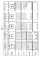
- FIGS. 1A to 1D are schematic diagrams each illustrating an example of an exposure apparatus which achieves a method of manufacturing a diffraction grating of an embodiment of the present invention
- FIG. 2 is a schematic diagram illustrating an example of a relation between a phase difference of a phase shift mask and a size thereof used for the exposure apparatus illustrated in FIGS. 1A to 1D ;
- FIGS. 3A to 3D are schematic diagrams each illustrating an example of a phase shift mask used for the exposure apparatus illustrated in FIGS. 1A to 1D ;
- FIG. 4 is a diagram illustrating an example of a simulation condition in simulation in simulation evaluation in the method of manufacturing the diffraction grating by using the exposure apparatus illustrated in FIGS. 1A to 1D ;
- FIG. 5 is a diagram illustrating an example of a relation between a phase shift and pattern ratio by the simulation in the simulation evaluation in the method of manufacturing the diffraction grating by using the exposure apparatus illustrated in FIGS. 1A to 1D ;
- FIG. 6 is a diagram illustrating an example of dependency of an exposure amount on a depth of the diffraction grating in the simulation evaluation in the method of manufacturing the diffraction grating by using the exposure apparatus illustrated in FIGS. 1A to 1D ;
- FIG. 7 is a diagram illustrating an example of a light intensity distribution in the simulation evaluation in the method of manufacturing the diffraction grating by using the exposure apparatus illustrated in FIGS. 1A to 1D ;
- FIG. 8 is a diagram illustrating an example of a contrast in the simulation evaluation in the method of manufacturing the diffraction grating by using the exposure apparatus illustrated in FIGS. 1A to 1D ;
- FIG. 9 is a diagram illustrating an example of requirement specification of the diffraction grating in application evaluation to a required specification of the diffraction grating in the method of manufacturing the diffraction grating by using the exposure apparatus illustrated in FIGS. 1A to 1D ;
- FIG. 10 is a diagram illustrating an example of dependency of a pitch in the application evaluation to the required specification of the diffraction grating in the method of manufacturing the diffraction grating by using the exposure apparatus illustrated in FIGS. 1A to 1D ;
- FIG. 11 is a diagram illustrating an example of a phase shift required for the required specification of the diffraction grating illustrated in FIG. 9 in the application evaluation to the required specification of the diffraction grating in the method of manufacturing the diffraction grating by using the exposure apparatus illustrated in FIGS. 1A to 1D ;
- FIGS. 12A and 12B are schematic diagrams each illustrating a modification example of the phase shift mask used for the exposure apparatus illustrated in FIGS. 1A to 1D .
- the invention will be described in a plurality of sections or embodiments when required as a matter of convenience. However, these sections or embodiments are not irrelevant to each other unless otherwise stated, and the one relates to the entire or a part of the other as a modification example, details, or a supplementary explanation thereof. Also, in the embodiments described below, when referring to the number of elements (including number of pieces, values, amount, range, and others), the number of the elements is not limited to a specific number unless otherwise stated or except the case where the number is apparently limited to a specific number in principle. The number larger or smaller than the specified number is also applicable.
- the components are not always indispensable unless otherwise stated or except the case where the components are apparently indispensable in principle.
- the shape of the components, positional relation thereof, and others are described, the substantially approximate and similar shapes and others are included therein unless otherwise stated or except the case where it is conceivable that they are apparently excluded in principle. The same goes for the numerical value and the range described above.
- the embodiment of the present invention has the following feature so as to be applied to a phase shift mask, and to a method of forming an asymmetric pattern by using the phase shift mask, and further, to a method of manufacturing a diffraction grating by using the phase shift mask, and to a method of manufacturing a semiconductor device (as an example, a corresponding component, symbol, or others is added in parentheses ( )).
- the method of forming the asymmetric pattern by using the above-described phase shift mask ( 30 ) has a feature of formation of the above-described asymmetric pattern on a substrate by transmitting light emitted from a light source through the above-described phase shift mask, and by exposing a photosensitive material on a surface of a substrate by providing interference between zero diffraction order light and positive first diffraction order light which are generated by the transmission through the above-described phase shift mask onto the surface of the substrate.
- the method of manufacturing the diffraction grating by using the above-described phase shift mask ( 30 ) has a feature of formation of the diffraction grating which has the blazed cross-sectional shape on a substrate by transmitting light emitted from a light source (illumination light source 10 ) through the above-described phase shift mask, and by exposing a photosensitive material (photoresist 60 ) on a surface of a substrate by providing interference between zero diffraction order light and positive first diffraction order light which are generated by the transmission through the above-described phase shift mask onto the surface of the substrate (Si wafer 50 ).
- the method of manufacturing the semiconductor device by using the above-described phase shift mask ( 30 ) has a feature of formation of the above-described asymmetric cross-sectional shape on a semiconductor substrate by transmitting light emitted from a light source through the above-described phase shift mask, and by exposing a photosensitive material on a surface of a semiconductor substrate by providing interference between zero diffraction order light and positive first diffraction order light which are generated by the transmission through the above-described phase shift mask onto the surface of the semiconductor substrate.
- FIGS. 1A to 12B An embodiment of the present invention will be explained by using FIGS. 1A to 12B .
- FIGS. 1A to 1D are schematic diagrams each illustrating an example of this exposure apparatus, FIG. 1A illustrates outline of the exposure apparatus, FIG. 1B illustrates a shape of a mask, FIG. 1C illustrates alight intensity distribution on a pupil plane of a projection lens, and FIG. 1D illustrates a shape of a photoresist on a Si wafer.
- the exposure apparatus in the present embodiment is configured of an illumination light source 10 , a collective lens 20 , the phase shift mask 30 , a projection lens 40 , and others.
- This exposure apparatus is an apparatus to which a technique of forming a three-dimensional resist pattern by using the phase shift mask 30 is applied and which exposes a photoresist 60 applied to a surface of a Si wafer 50 to light.
- the illumination light source 10 is to be a light source for the exposure.
- this illumination light source 10 for example, g-line, i-line, or an excimer laser of KrF, ArF, or others is used.
- the collective lens 20 is a lens for collecting light emitted from the illumination light source 10 onto the phase shift mask 30 .
- the phase shift mask 30 has a predetermined periodic pattern so that the pattern is arranged in accordance with a blazed-shape pitch of the diffraction grating.
- the periodic pattern of this phase shift mask 30 has a light shield part 31 which shields light, and a light transmission part 32 which transmits light.
- the light transmission part 32 is configured of a first light transmission part 32 a having no phase shift (0°) and a second light transmission part 32 b having a phase shift ( ⁇ ).
- a set of the light shield part 31 , the first light transmission part 32 a , and the second light transmission part 32 b is arranged periodically.
- the projection lens 40 is a lens for projecting the periodic pattern of the light shield part 31 and the light transmission part 32 of the phase shift mask 30 onto the photoresist 60 of the Si wafer 50 .
- a pupil plane 41 of this projection lens 40 the light intensity distribution as illustrated in FIG. 1C (illustrated in detail in FIGS. 3A to 3D ) is provided. That is, it has been found out that ⁇ (negative) first diffraction order light disappears due to the transmission through the phase shift mask 30 so as to generate the zero diffraction order light and the positive first diffraction order light.
- a reduced projection exposure apparatus which projects the pattern of the phase shift mask 30 so as to reduce the pattern will be described as an example.
- the negative first diffraction order light disappears by using the phase shift mask 30 having the periodically-arranged light shield part 31 and light transmission part 32 (first light transmission part 32 a having no phase shift and second light transmission part 32 b having a phase shift), and such a blazed cross-sectional shape that a resist of the photoresist 60 is not patterned down to the Si wafer 50 can be formed as illustrated in FIG. 1D (illustrated in detail in FIGS. 3A to 3D ).
- a depth (angle) of the blazed cross-sectional shape can be also adjusted by changing a phase difference of the light transmission part 32 and a ratio in the width among the light shield part 31 , the first light transmission part 32 a , and the second light transmission part 32 b.
- the photoresist 60 on the surface of the Si wafer 50 is exposed by using the exposure apparatus as described above, the light emitted from the illumination light source 10 is transmitted through the phase shift mask 30 , and the photoresist 60 on this Si wafer 50 is exposed to light by providing interference between the zero diffraction order light and the positive first diffraction order light which are generated by the transmission through this phase shift mask 30 onto the surface of the Si wafer 50 , so that the diffraction grating having the photoresist 60 which has the blazed cross-sectional shape is formed on the Si wafer 50 .
- FIG. 2 is a schematic diagram illustrating an example of a relation between a phase difference of this phase shift mask and a size thereof.
- FIGS. 3A to 3D are schematic diagrams each illustrating an example (example of a specification 4 in FIG. 5 described later) of this phase shift mask, FIG. 3A illustrates a planar shape of the phase shift mask, FIG. 3B illustrates a cross-sectional shape of the phase shift mask, FIG. 3C illustrates a light intensity distribution on the pupil plane of the projection lens obtained by using this phase shift mask, and FIG. 3D illustrates a shape of the photoresist on the Si wafer obtained by using this phase shift mask.
- the periodic pattern of the phase shift mask 30 has a set of the light shield part 31 , the first light transmission part 32 a which is adjacent to this light shield part 31 and which has no phase shift (0°), and the second light transmission part 32 b which is adjacent to this first light transmission part 32 a and which has a phase shift ( ⁇ ) arranged periodically in a planar shape.
- the phase shift mask 30 illustrated in this FIG. 3A 5 sets are illustrated so that five light shield parts 31 (illustrated with a black color), five first light transmission parts 32 a (illustrated with a white color), and five second light transmission parts 32 b (illustrated with a dot) are provided.
- a cross-sectional shape of the periodic pattern of this phase shift mask 30 is formed so as to have a concave portion in which the first light transmission part 32 a and the second light transmission part 32 b are integrally formed, and a thickness of the second light transmission part 32 b corresponding to this concave portion is thinner than a thickness of the first light transmission part 32 a .
- a metal film is formed as the light shield part 31 .
- the light transmission part 32 configured of the first light transmission part 32 a and the second light transmission part 32 b is made of quartz glass or others, and the light shield part 31 is made of a metal film of Cr or others.
- the photoresist 60 on the surface of the Si wafer 50 can be exposed to light.
- the negative first diffraction order light can disappear, and the zero diffraction order light and the positive first diffraction order light can be generated as illustrated in FIG. 3C .
- the photoresist 60 on the surface of the Si wafer 50 can be exposed to light so that the shape of the photoresist 60 on the Si wafer 50 can be as the cross-sectional shape having the blazed shape (angle, depth) in which the photoresist is not etched down to the Si wafer 50 as illustrated in FIG. 3D .
- phase shift mask 30 in which the light shield part 31 and the light transmission part 32 (including the first light transmission part 32 a having no phase shift and the second light transmission part 32 b having the phase shift) are periodically arranged is prepared.
- This phase shift mask 30 is illustrated in, for example, FIGS. 2, 3A, and 3B described above.
- a photoresist is applied to a Si wafer for test exposure by using a spin coater, and then, prebaking is performed.
- step (3) Onto the Si wafer of the above-described step (2), the pattern is transferred by the reduced projection exposure apparatus using the phase shift mask 30 . At this time, the transfer is repeated to obtain a plurality of shots so that each of a focus value of the exposure apparatus, an exposure amount thereof, and a numerical aperture of an exposure lens thereof is changed at a plurality of steps as changing a region on the Si wafer.
- a cross-sectional shape of a three-dimensional photoresist pattern formed on the Si wafer of the above-described step (4) is measured, and a shot at which this cross-sectional shape is most matched with a cross-sectional shape (for example, in FIG. 3D in the present embodiment) of a diffraction grating to be desirably manufactured is selected, and the focus value of the shot and the exposure amount thereof are recorded as an optimal exposure condition.
- the procedure proceeds to the following step (7) in order to manufacture a diffraction grating to be a product.
- the photoresist 60 is applied to the Si wafer 50 for manufacturing the diffraction grating by using a spin coater, and then, prebaking is performed.
- the transferring is performed by the reduced projection exposure apparatus using the phase shift mask 30 .
- the focus value and the exposure amount under the optimal exposure condition which have been recorded in the above-described step (6) are set.
- the diffraction grating formed in the above-described step (10) is cut out into an appropriate size. In this manner, a diffraction grating product in which the blazed-shape photoresist 60 is formed on the Si wafer 50 , and further, in which the Al film is formed on the photoresist 60 is completed.
- FIGS. 4 to 8 simulation evaluation in the method of manufacturing the diffraction grating by using the exposure apparatus illustrated in FIGS. 1A to 1D described above will be explained.
- FIG. 4 is a diagram illustrating an example of a simulation condition in the simulation. As illustrated in FIG. 4 , condition parameters of the simulation are as follows.
- FIG. 5 is a diagram illustrating an example of the relation between the phase shift and the pattern ratio in the simulation.
- the exposure amount of the exposure condition is assumed to be 50 mJ/cm 2 , 100 mJ/cm 2 , 200 mJ/cm 2 and 300 mJ/cm 2 .
- the first diffraction order light is stronger as the specification is closer to the specification 1
- the first diffraction order light is weaker as the specification is closer to the specification 5 .
- the depth (blaze angle) of the resist shape of the photoresist 60 can be adjusted by changing the phase shift and the pattern ratio. More specifically, it is found out that a diffraction grating whose depth is shallow can be formed by changing the phase shift as 90° ⁇ 60° ⁇ 45° ⁇ 30° ⁇ 15°.
- 300 mJ/cm 2 in the specification 1 200 mJ/cm 2 and 300 mJ/cm 2 in the specification 2
- 100 mJ/cm 2 and 200 mJ/cm 2 in the specification 3 100 mJ/cm 2 and 200 mJ/cm 2 in the specification 4
- 100 mJ/cm 2 and 200 mJ/cm 2 in the specification 5 can be used for the diffraction grating which has the blazed cross-sectional shape.
- the depth can be increased in 300 mJ/cm 2 of the specification 1 , and the depth can be decreased in 100 mJ/cm 2 of the specification 5 , so that the depth can be adjusted by changing the phase shift and the pattern ratio in accordance with the required specification for the diffraction grating.
- FIG. 6 is a diagram illustrating an example of dependency of the exposure amount on the depth of the diffraction grating.
- a horizontal axis indicates the exposure amount [mJ/cm 2 ]
- a vertical axis indicates the depth [ ⁇ m]
- the specification 1 90°
- the specification 2 60°
- the specification 3 45°
- the specification 4 (30°)
- the specification 5 15°
- the depth can be adjusted by changing the phase shift and the pattern ratio.
- the diffraction grating whose depth is shallow can be formed by changing the phase shift from 90° to 15°.
- FIG. 7 is a diagram illustrating an example of the light intensity distribution.
- a horizontal axis indicates an “x” position [ ⁇ m]
- a vertical axis indicates the light intensity
- the specification 1 90°
- the specification 2 60°
- the specification 3 45°
- the specification 4 (30°)
- the specification 5 15°
- FIG. 8 is a diagram illustrating an example of contrast.
- a horizontal axis indicates the phase
- a vertical axis indicates the contrast. From FIG. 8 , it is found out that the contrast is changed by changing the phase shift and the pattern ratio.
- the contrast is changed by changing the phase shift and the pattern ratio, and as a result, the diffraction grating whose depth (blaze angle) is different can be obtained.
- FIGS. 9 to 11 application evaluation to the required specification of the diffraction grating in the method of manufacturing the diffraction grating by using the exposure apparatus illustrated in FIGS. 1A to 1D described above will be explained.
- the required specification of the diffraction grating described here is an example, and the present invention is not limited to this example.
- FIG. 9 is a diagram illustrating an example of the required specification of the diffraction grating. As illustrated in FIG. 9 , the groove density [grooves/mm], Pitch [ ⁇ m], Angle [°], Depth [ ⁇ m] will be studied as the required specification of the diffraction grating.
- FIG. 10 is a diagram illustrating an example of pitch dependency.
- FIG. 11 is a diagram illustrating an example of a phase shift required for the required specification of the diffraction grating illustrated in FIG. 9 .
- phase shift to be required 60° or smaller is required as the phase. Also, the manufacturing of 30 ⁇ m pitch is impossible.
- FIGS. 12A and 12B illustrate schematic diagrams each illustrating the modification example of this phase shift mask
- FIG. 12A illustrates a planar shape of the phase shift mask
- FIG. 12B illustrates a cross-sectional shape of the phase shift mask.
- the first light transmission part 32 a having no phase shift (0°) and the second light transmission part 32 b having the phase shift ( ⁇ ) are arranged to be opposite to each other in FIG. 3A in a planar shape. That is, a set of the light shield part 31 , the second light transmission part 32 b which is adjacent to this light shield part 31 and which has the phase shift ( ⁇ ), and the first light transmission part 32 a which is adjacent to this second light transmission part 32 b and which has no phase shift (0°) is periodically arranged.
- the set of the light shield part 31 , the second light transmission part 32 b , and the first light transmission part 32 a is periodically arranged, and a thickness of the second light transmission part 32 b corresponding to this concave portion is formed to be thinner than a thickness of the first light transmission part 32 a.
- phase shift mask 30 having such a shape
- positive first diffraction order light disappears, and zero diffraction order light and negative first diffraction order light can be generated by transmitting the light emitted from the illumination light source 10 through this phase shift mask 30 , and the photoresist 60 on the surface of this Si wafer 50 is exposed to light by providing interference between the zero diffraction order light and the negative first diffraction order light onto a surface of the Si wafer 50 , so that the shape of the photoresist 60 on the Si wafer 50 can be the blazed cross-sectional shape in which the photoresist is not etched down to the Si wafer 50 .
- the light shield part 31 and the light transmission part 32 (the first light transmission part 32 a having no phase shift and the second light transmission part 32 b having the phase shift) are periodically arranged
- the light emitted from the illumination light source 10 is transmitted through the phase shift mask 30
- interference between the zero diffraction order light and the positive first diffraction order light which are generated by the transmission through this phase shift mask 30 is provided onto the surface of the Si wafer 50
- the photoresist 60 on this Si wafer 50 is exposed, and the diffraction grating which has the blazed cross-sectional shape is formed on the Si wafer 50 , so that effects described below can be obtained.
- the manufacturing time (for, for example, mask preparation: one month/mask ⁇ one day/mask) can be shorter, and accuracy can be improved more than those of a ruling engine.
- the manufacturing time can be shorter, and the accuracy of the product can be improved more than those of the holographic exposure because an additional process such as oblique etching is not required.
- the photolithography technique is a technique which forms a pattern by using a short wavelength light source for handling microfabrication of the semiconductor product and high accuracy of the microfabrication, and therefore, can achieve the higher accuracy than that of the ruling engine which mechanically rules by using a diamond tool having the same size as a diffraction grating to be manufactured.
- inclination can be provided to an optical image by performing the exposure once, and therefore, the additional process is not required. Therefore, the manufacturing variation can be reduced, and the process accuracy can be improved more than those of the holographic exposure which requires the additional process.
- the lithography technique is a technique of transferring any mask layout pattern onto the photoresist 60 applied to the Si wafer 50 , a diffraction grating whose depth (blaze angle) is changed can be formed.
- the depth of the blazed cross-sectional shape of the diffraction grating can be as the depth which does not reach the Si wafer 50 .
- the Si wafer 50 between the patterns of the diffraction grating can be prevented from being exposed.
- the method of manufacturing the diffraction grating according to the present invention has been explained.
- the present invention is not limited to the method of manufacturing the diffraction grating, and can be applied to the item (4) the method of manufacturing the semiconductor device by using the above-described phase shift mask ( 30 ) described in the summary of the embodiment of the present invention described above.
- the asymmetric cross-sectional shape can be formed on a semiconductor substrate by applying the embodiment described above.
- this asymmetric cross-sectional shape by applying not only a photosensitive material but also a publicly-known semiconductor etching method, the cross-sectional shape of the photosensitive material is transferred to the semiconductor substrate, so that the asymmetric cross-sectional shape can be formed on the semiconductor substrate.
- the present invention can be applied to the item (2) the method of forming the asymmetric pattern by using the above-described phase shift mask ( 30 ) described in the summary of the embodiment of the present invention described above, and can be widely applied as a technique of forming the asymmetric pattern on the substrate.
- the technique of forming the asymmetric pattern by using the phase shift mask of the present invention can be particularly used for the method of manufacturing the blazed diffraction grating which has the blazed cross-sectional shape. Also, the technique can be used for the method of manufacturing the semiconductor device including the asymmetric shape.
Landscapes
- Physics & Mathematics (AREA)
- General Physics & Mathematics (AREA)
- Exposure And Positioning Against Photoresist Photosensitive Materials (AREA)
- Preparing Plates And Mask In Photomechanical Process (AREA)
- Diffracting Gratings Or Hologram Optical Elements (AREA)
- Engineering & Computer Science (AREA)
- Plasma & Fusion (AREA)
Abstract
Description
- (1) Illumination condition . . . Wave length=365 nm, Light source=circle, σ=0.3, NA=0.63
- (2) Mask condition . . . .
- Mask pattern=0.6 μm pitch,
- Mask size=first light transmission part (0°): second light transmission part (θ(phase)): light shield part (Cr)
- =
specification 1 - =150 nm: 150 nm (90°): 300 nm,
- =
specification 2 - =200 nm: 200 nm (60°): 200 nm,
- =
specification 3 - =225 nm: 225 nm (45°): 150 nm,
- =
specification 4 - =250 nm: 250 nm (30°): 100 nm,
- =
specification 5 - =275 nm: 275 nm (15°): 50 nm
- (3) Exposure condition . . . Exposure amount=100 mJ/cm2 to 300 mJ/cm2,
- Focus value=0.0 μm
- (4) Resist condition . . . Resist thickness=2000 nm
-
- 10 illumination light source
- 20 collective lens
- 30 phase shift mask
- 31 light shield part
- 32 light transmission part
- 32 a first light transmission part
- 32 b second light transmission part
- 40 projection lens
- 41 pupil plane
- 50 Si wafer
- 60 photoresist
Claims (6)
Applications Claiming Priority (3)
| Application Number | Priority Date | Filing Date | Title |
|---|---|---|---|
| JP2011222907A JP5841797B2 (en) | 2011-10-07 | 2011-10-07 | Manufacturing method of diffraction grating |
| JP2011-222907 | 2011-10-07 | ||
| PCT/JP2012/073479 WO2013051384A1 (en) | 2011-10-07 | 2012-09-13 | Phase shift mask, asymmetric pattern forming method, diffraction grating manufacturing method and semiconductor device manufacturing method |
Publications (2)
| Publication Number | Publication Date |
|---|---|
| US20140302679A1 US20140302679A1 (en) | 2014-10-09 |
| US9390934B2 true US9390934B2 (en) | 2016-07-12 |
Family
ID=48043548
Family Applications (1)
| Application Number | Title | Priority Date | Filing Date |
|---|---|---|---|
| US14/350,314 Expired - Fee Related US9390934B2 (en) | 2011-10-07 | 2012-09-13 | Phase shift mask, method of forming asymmetric pattern, method of manufacturing diffraction grating, and method of manufacturing semiconductor device |
Country Status (5)
| Country | Link |
|---|---|
| US (1) | US9390934B2 (en) |
| EP (1) | EP2765455A4 (en) |
| JP (1) | JP5841797B2 (en) |
| CN (1) | CN103998984B (en) |
| WO (1) | WO2013051384A1 (en) |
Families Citing this family (4)
| Publication number | Priority date | Publication date | Assignee | Title |
|---|---|---|---|---|
| WO2016152212A1 (en) * | 2015-03-24 | 2016-09-29 | Hoya株式会社 | Mask blanks, phase shift mask, method for manufacturing phase shift mask, and method for manufacturing semiconductor device |
| JP6370755B2 (en) | 2015-09-11 | 2018-08-08 | 東芝メモリ株式会社 | Mask and pattern forming method |
| CN115712164B (en) * | 2023-01-06 | 2023-04-21 | 山东省科学院激光研究所 | A wavelength-tunable phase-shift grating manufacturing system and manufacturing method |
| KR102950506B1 (en) * | 2024-04-17 | 2026-04-08 | 한양대학교 산학협력단 | EUV interference lithography system |
Citations (15)
| Publication number | Priority date | Publication date | Assignee | Title |
|---|---|---|---|---|
| JPS63187202A (en) | 1987-01-30 | 1988-08-02 | Hitachi Ltd | blazed holographic grating |
| JPS63271265A (en) | 1986-12-06 | 1988-11-09 | Kuraray Co Ltd | Production of transmissivity modulation type photomask and production of diffraction gtating using the photomask |
| JPS6473378A (en) | 1987-09-14 | 1989-03-17 | Fujitsu Ltd | Formation of surface relief type hologram |
| US4842969A (en) | 1986-12-06 | 1989-06-27 | Kuraray Company, Ltd. | Transmittance modulation photomask, process for producing the same, and process for producing diffraction gratings using the same |
| JPH04186829A (en) | 1990-11-21 | 1992-07-03 | Fujitsu Ltd | Manufacture of semiconductor device |
| JPH05224398A (en) | 1992-02-12 | 1993-09-03 | Kuraray Co Ltd | Transmittance modulation type photomask and method of manufacturing optical component using the same |
| JPH0620940A (en) | 1992-06-29 | 1994-01-28 | Shimadzu Corp | Manufacture of resist pattern |
| JP2000058970A (en) | 1998-08-04 | 2000-02-25 | Toshiba Corp | Optical functional element, method for manufacturing the same, and optical communication system |
| JP2002055435A (en) | 2000-08-09 | 2002-02-20 | Toshiba Corp | Test mark and method of measuring focus and aberration using the same |
| US20030020901A1 (en) | 2001-07-27 | 2003-01-30 | Gerhard Kunkel | Grating patterns and method for determination of azimuthal and radial aberration |
| JP2005037598A (en) | 2003-07-18 | 2005-02-10 | Toshiba Corp | Reticle, exposure apparatus inspection system, exposure apparatus inspection method, and reticle manufacturing method |
| US20050112475A1 (en) | 2003-08-27 | 2005-05-26 | Takashi Sato | Photomask, method of lithography, and method for manufacturing the photomask |
| JP2005157118A (en) | 2003-11-27 | 2005-06-16 | Shimadzu Corp | Blazed holographic grating, manufacturing method thereof, and replica grating |
| US20060019180A1 (en) | 2004-07-26 | 2006-01-26 | Hiroshi Nomura | Photo mask, focus measuring method using the mask, and method of manufacturing semiconductor device |
| US20090190118A1 (en) | 2008-01-28 | 2009-07-30 | Kazuya Fukuhara | Exposure apparatus inspection mask, and method of inspecting exposure apparatus using exposure apparatus inspection mask |
-
2011
- 2011-10-07 JP JP2011222907A patent/JP5841797B2/en not_active Expired - Fee Related
-
2012
- 2012-09-13 EP EP12837928.6A patent/EP2765455A4/en not_active Withdrawn
- 2012-09-13 CN CN201280048495.4A patent/CN103998984B/en not_active Expired - Fee Related
- 2012-09-13 US US14/350,314 patent/US9390934B2/en not_active Expired - Fee Related
- 2012-09-13 WO PCT/JP2012/073479 patent/WO2013051384A1/en not_active Ceased
Patent Citations (23)
| Publication number | Priority date | Publication date | Assignee | Title |
|---|---|---|---|---|
| JPS63271265A (en) | 1986-12-06 | 1988-11-09 | Kuraray Co Ltd | Production of transmissivity modulation type photomask and production of diffraction gtating using the photomask |
| US4842969A (en) | 1986-12-06 | 1989-06-27 | Kuraray Company, Ltd. | Transmittance modulation photomask, process for producing the same, and process for producing diffraction gratings using the same |
| JPS63187202A (en) | 1987-01-30 | 1988-08-02 | Hitachi Ltd | blazed holographic grating |
| JPS6473378A (en) | 1987-09-14 | 1989-03-17 | Fujitsu Ltd | Formation of surface relief type hologram |
| JPH04186829A (en) | 1990-11-21 | 1992-07-03 | Fujitsu Ltd | Manufacture of semiconductor device |
| JPH05224398A (en) | 1992-02-12 | 1993-09-03 | Kuraray Co Ltd | Transmittance modulation type photomask and method of manufacturing optical component using the same |
| JPH0620940A (en) | 1992-06-29 | 1994-01-28 | Shimadzu Corp | Manufacture of resist pattern |
| US6587619B1 (en) | 1998-08-04 | 2003-07-01 | Kabushiki Kaisha Toshiba | Optical functional devices their manufacturing method and optical communication system |
| JP2000058970A (en) | 1998-08-04 | 2000-02-25 | Toshiba Corp | Optical functional element, method for manufacturing the same, and optical communication system |
| JP2002055435A (en) | 2000-08-09 | 2002-02-20 | Toshiba Corp | Test mark and method of measuring focus and aberration using the same |
| US20020021434A1 (en) | 2000-08-09 | 2002-02-21 | Kabushiki Kasiha | Evaluation mask, focus measuring method and aberration measuring method |
| US20030020901A1 (en) | 2001-07-27 | 2003-01-30 | Gerhard Kunkel | Grating patterns and method for determination of azimuthal and radial aberration |
| JP2005037598A (en) | 2003-07-18 | 2005-02-10 | Toshiba Corp | Reticle, exposure apparatus inspection system, exposure apparatus inspection method, and reticle manufacturing method |
| US7432021B2 (en) | 2003-07-18 | 2008-10-07 | Kabushiki Kaisha Toshiba | Reticle, apparatus for monitoring optical system, method for monitoring optical system, and method for manufacturing reticle |
| US7812972B2 (en) | 2003-07-18 | 2010-10-12 | Kabushiki Kaisha Toshiba | Reticle, apparatus for monitoring optical system, method for monitoring optical system, and method for manufacturing reticle |
| US20050112475A1 (en) | 2003-08-27 | 2005-05-26 | Takashi Sato | Photomask, method of lithography, and method for manufacturing the photomask |
| JP2005157118A (en) | 2003-11-27 | 2005-06-16 | Shimadzu Corp | Blazed holographic grating, manufacturing method thereof, and replica grating |
| US20050130072A1 (en) | 2003-11-27 | 2005-06-16 | Shimadzu Corporation | Blazed holographic grating, method for producing the same and replica grating |
| US20060019180A1 (en) | 2004-07-26 | 2006-01-26 | Hiroshi Nomura | Photo mask, focus measuring method using the mask, and method of manufacturing semiconductor device |
| EP1621932A1 (en) | 2004-07-26 | 2006-02-01 | Kabushi Kaisha Toshiba | Photo mask and focus measuring method using the mask |
| JP2006039148A (en) | 2004-07-26 | 2006-02-09 | Toshiba Corp | Photomask, focus measurement method using the same, and semiconductor device manufacturing method |
| US20090190118A1 (en) | 2008-01-28 | 2009-07-30 | Kazuya Fukuhara | Exposure apparatus inspection mask, and method of inspecting exposure apparatus using exposure apparatus inspection mask |
| JP2009175587A (en) | 2008-01-28 | 2009-08-06 | Toshiba Corp | Exposure apparatus inspection mask, manufacturing method thereof, and exposure apparatus inspection method using exposure apparatus inspection mask |
Non-Patent Citations (3)
| Title |
|---|
| H. Nomura, "New phase shift gratings for measuring aberrations," Optical Microlithography XIV, Proceedings of SPIE vol. 4346 (2001). |
| International Search Report issued in International Application No. PCT/JP2012/073479 with Date of mailing Oct. 23, 2012, with English Translation. |
| Supplementary European Search Report EP Application No. 12837928-6 dated Nov. 30, 2015. |
Also Published As
| Publication number | Publication date |
|---|---|
| CN103998984B (en) | 2017-05-24 |
| WO2013051384A1 (en) | 2013-04-11 |
| EP2765455A1 (en) | 2014-08-13 |
| EP2765455A4 (en) | 2015-12-30 |
| CN103998984A (en) | 2014-08-20 |
| JP5841797B2 (en) | 2016-01-13 |
| US20140302679A1 (en) | 2014-10-09 |
| JP2013083759A (en) | 2013-05-09 |
Similar Documents
| Publication | Publication Date | Title |
|---|---|---|
| JP3287236B2 (en) | Manufacturing method of diffractive optical element | |
| US20140092384A1 (en) | Diffraction grating manufacturing method, spectrophotometer, and semiconductor device manufacturing method | |
| KR101544274B1 (en) | Photomask for manufacturing a display device and pattern transfer method | |
| CN106019850A (en) | EUV focus monitoring systems and methods | |
| US20090148780A1 (en) | Method for correcting mask pattern, and exposure mask | |
| US20090190118A1 (en) | Exposure apparatus inspection mask, and method of inspecting exposure apparatus using exposure apparatus inspection mask | |
| JP2014500623A (en) | Method and apparatus for printing a high-resolution two-dimensional periodic pattern | |
| US9390934B2 (en) | Phase shift mask, method of forming asymmetric pattern, method of manufacturing diffraction grating, and method of manufacturing semiconductor device | |
| CN109388018B (en) | Method for correcting photomask, method for manufacturing photomask, and method for manufacturing display device | |
| US20100304279A1 (en) | Manufacturing method of phase shift mask, creating method of mask data of phase shift mask, and manufacturing method of semiconductor device | |
| JP2008089923A (en) | Method of manufacturing optical element | |
| JP6356510B2 (en) | Exposure method and exposure apparatus | |
| TW201327063A (en) | Method for manufacturing periodic structures on a surface of a substrate | |
| JP2011118344A (en) | Method for forming three-dimensional pattern | |
| TW202144928A (en) | Exposure apparatus, exposure method, and method for producing object that suppresses deterioration of transfer performance for transferring a pattern to a substrate in broadband illumination light | |
| TWI847583B (en) | Exposure device and method for manufacturing article | |
| JP2013246340A (en) | Photomask and method of manufacturing the same, and pattern exposure method | |
| JP2014228838A (en) | Method for forming fine pattern | |
| JP2005172877A (en) | Resist pattern forming method, optical element manufacturing method, substrate manufacturing method, optical element, and exposure apparatus | |
| US9500961B2 (en) | Pattern formation method and exposure apparatus | |
| JP2003021709A (en) | Binary optics element | |
| JP2005275000A (en) | Mask used for manufacturing optical element, and method for manufacturing optical element using the mask | |
| JP2017015863A (en) | Photomask, method for designing photomask, photomask blank, and method for manufacturing display device | |
| JPH11307444A (en) | Projection exposure apparatus and device manufacturing method using the same | |
| JP2012203357A (en) | Photomask and method for manufacturing the same |
Legal Events
| Date | Code | Title | Description |
|---|---|---|---|
| AS | Assignment |
Owner name: HITACHI HIGH-TECHNOLOGIES CORPORATION, JAPAN Free format text: ASSIGNMENT OF ASSIGNORS INTEREST;ASSIGNORS:KAKUTA, KAZUYUKI;ONOZUKA, TOSHIHIKO;MATSUI, SHIGERU;AND OTHERS;SIGNING DATES FROM 20140326 TO 20140403;REEL/FRAME:032620/0314 |
|
| STCF | Information on status: patent grant |
Free format text: PATENTED CASE |
|
| MAFP | Maintenance fee payment |
Free format text: PAYMENT OF MAINTENANCE FEE, 4TH YEAR, LARGE ENTITY (ORIGINAL EVENT CODE: M1551); ENTITY STATUS OF PATENT OWNER: LARGE ENTITY Year of fee payment: 4 |
|
| AS | Assignment |
Owner name: HITACHI HIGH-TECH CORPORATION, JAPAN Free format text: CHANGE OF NAME AND ADDRESS;ASSIGNOR:HITACHI HIGH-TECHNOLOGIES CORPORATION;REEL/FRAME:052259/0227 Effective date: 20200212 |
|
| FEPP | Fee payment procedure |
Free format text: MAINTENANCE FEE REMINDER MAILED (ORIGINAL EVENT CODE: REM.); ENTITY STATUS OF PATENT OWNER: LARGE ENTITY |
|
| LAPS | Lapse for failure to pay maintenance fees |
Free format text: PATENT EXPIRED FOR FAILURE TO PAY MAINTENANCE FEES (ORIGINAL EVENT CODE: EXP.); ENTITY STATUS OF PATENT OWNER: LARGE ENTITY |
|
| STCH | Information on status: patent discontinuation |
Free format text: PATENT EXPIRED DUE TO NONPAYMENT OF MAINTENANCE FEES UNDER 37 CFR 1.362 |
|
| FP | Lapsed due to failure to pay maintenance fee |
Effective date: 20240712 |