US9368084B2 - Display apparatus and method thereof - Google Patents
Display apparatus and method thereof Download PDFInfo
- Publication number
- US9368084B2 US9368084B2 US12/351,095 US35109509A US9368084B2 US 9368084 B2 US9368084 B2 US 9368084B2 US 35109509 A US35109509 A US 35109509A US 9368084 B2 US9368084 B2 US 9368084B2
- Authority
- US
- United States
- Prior art keywords
- clock
- interconnection
- gate
- layer
- forming
- Prior art date
- Legal status (The legal status is an assumption and is not a legal conclusion. Google has not performed a legal analysis and makes no representation as to the accuracy of the status listed.)
- Active, expires
Links
Images


Classifications
-
- G—PHYSICS
- G09—EDUCATION; CRYPTOGRAPHY; DISPLAY; ADVERTISING; SEALS
- G09G—ARRANGEMENTS OR CIRCUITS FOR CONTROL OF INDICATING DEVICES USING STATIC MEANS TO PRESENT VARIABLE INFORMATION
- G09G3/00—Control arrangements or circuits, of interest only in connection with visual indicators other than cathode-ray tubes
- G09G3/20—Control arrangements or circuits, of interest only in connection with visual indicators other than cathode-ray tubes for presentation of an assembly of a number of characters, e.g. a page, by composing the assembly by combination of individual elements arranged in a matrix no fixed position being assigned to or needed to be assigned to the individual characters or partial characters
- G09G3/34—Control arrangements or circuits, of interest only in connection with visual indicators other than cathode-ray tubes for presentation of an assembly of a number of characters, e.g. a page, by composing the assembly by combination of individual elements arranged in a matrix no fixed position being assigned to or needed to be assigned to the individual characters or partial characters by control of light from an independent source
- G09G3/36—Control arrangements or circuits, of interest only in connection with visual indicators other than cathode-ray tubes for presentation of an assembly of a number of characters, e.g. a page, by composing the assembly by combination of individual elements arranged in a matrix no fixed position being assigned to or needed to be assigned to the individual characters or partial characters by control of light from an independent source using liquid crystals
- G09G3/3611—Control of matrices with row and column drivers
- G09G3/3674—Details of drivers for scan electrodes
-
- G—PHYSICS
- G02—OPTICS
- G02F—OPTICAL DEVICES OR ARRANGEMENTS FOR THE CONTROL OF LIGHT BY MODIFICATION OF THE OPTICAL PROPERTIES OF THE MEDIA OF THE ELEMENTS INVOLVED THEREIN; NON-LINEAR OPTICS; FREQUENCY-CHANGING OF LIGHT; OPTICAL LOGIC ELEMENTS; OPTICAL ANALOGUE/DIGITAL CONVERTERS
- G02F1/00—Devices or arrangements for the control of the intensity, colour, phase, polarisation or direction of light arriving from an independent light source, e.g. switching, gating or modulating; Non-linear optics
- G02F1/01—Devices or arrangements for the control of the intensity, colour, phase, polarisation or direction of light arriving from an independent light source, e.g. switching, gating or modulating; Non-linear optics for the control of the intensity, phase, polarisation or colour
- G02F1/13—Devices or arrangements for the control of the intensity, colour, phase, polarisation or direction of light arriving from an independent light source, e.g. switching, gating or modulating; Non-linear optics for the control of the intensity, phase, polarisation or colour based on liquid crystals, e.g. single liquid crystal display cells
- G02F1/133—Constructional arrangements; Operation of liquid crystal cells; Circuit arrangements
-
- G—PHYSICS
- G09—EDUCATION; CRYPTOGRAPHY; DISPLAY; ADVERTISING; SEALS
- G09G—ARRANGEMENTS OR CIRCUITS FOR CONTROL OF INDICATING DEVICES USING STATIC MEANS TO PRESENT VARIABLE INFORMATION
- G09G3/00—Control arrangements or circuits, of interest only in connection with visual indicators other than cathode-ray tubes
- G09G3/20—Control arrangements or circuits, of interest only in connection with visual indicators other than cathode-ray tubes for presentation of an assembly of a number of characters, e.g. a page, by composing the assembly by combination of individual elements arranged in a matrix no fixed position being assigned to or needed to be assigned to the individual characters or partial characters
-
- G—PHYSICS
- G11—INFORMATION STORAGE
- G11C—STATIC STORES
- G11C19/00—Digital stores in which the information is moved stepwise, e.g. shift registers
- G11C19/18—Digital stores in which the information is moved stepwise, e.g. shift registers using capacitors as main elements of the stages
- G11C19/182—Digital stores in which the information is moved stepwise, e.g. shift registers using capacitors as main elements of the stages in combination with semiconductor elements, e.g. bipolar transistors, diodes
- G11C19/184—Digital stores in which the information is moved stepwise, e.g. shift registers using capacitors as main elements of the stages in combination with semiconductor elements, e.g. bipolar transistors, diodes with field-effect transistors, e.g. MOS-FET
-
- G—PHYSICS
- G09—EDUCATION; CRYPTOGRAPHY; DISPLAY; ADVERTISING; SEALS
- G09G—ARRANGEMENTS OR CIRCUITS FOR CONTROL OF INDICATING DEVICES USING STATIC MEANS TO PRESENT VARIABLE INFORMATION
- G09G2310/00—Command of the display device
- G09G2310/02—Addressing, scanning or driving the display screen or processing steps related thereto
- G09G2310/0264—Details of driving circuits
- G09G2310/0286—Details of a shift registers arranged for use in a driving circuit
-
- G—PHYSICS
- G09—EDUCATION; CRYPTOGRAPHY; DISPLAY; ADVERTISING; SEALS
- G09G—ARRANGEMENTS OR CIRCUITS FOR CONTROL OF INDICATING DEVICES USING STATIC MEANS TO PRESENT VARIABLE INFORMATION
- G09G2320/00—Control of display operating conditions
- G09G2320/04—Maintaining the quality of display appearance
- G09G2320/043—Preventing or counteracting the effects of ageing
Definitions
- the present invention relates to a display apparatus and a method thereof. More particularly, the present invention relates to a display apparatus capable of preventing a gate driver from malfunctioning due to high temperature aging, and a method of preventing a gate driver from malfunctioning.
- a liquid crystal display includes an LCD panel that displays an image.
- the LCD panel includes a bottom substrate, a top substrate facing the bottom substrate, and a liquid crystal layer interposed between the bottom and top substrates.
- the LCD panel includes a plurality of gate lines, a plurality of data lines, and a plurality of pixels connected with the gate and data lines.
- a gate driver is directly formed in the LCD panel through a thin film process to sequentially output a gate signal to the gate lines.
- the gate driver includes one shift register having a plurality of stages connected with each other one after another.
- each stage includes a plurality of transistors in order to output the gate signal to a corresponding gate line.
- Each transistor includes an amorphous silicon (“a-Si”) transistor.
- exemplary embodiments of the present invention provide a display apparatus capable of preventing a gate driver from malfunctioning due to high temperature aging.
- a display apparatus in an exemplary embodiment of the present invention, includes a display panel, a data driver and a gate driver.
- the display panel has gate lines, data lines and a plurality of pixels.
- the gate lines sequentially receive a gate signal.
- the data lines receive a data signal.
- the pixels display an image corresponding to the data signal in response to the gate signal.
- the data driver provides the data signal to the data lines.
- the gate driver is provided in the display panel and receives at least one clock to sequentially provide the gate lines with the gate signal in a high state corresponding to a high interval of the clock.
- the clock has delay time of about 2.0 ⁇ s or less.
- the gate driver includes amorphous silicon (“a-Si”) transistors and is formed on the display panel through a thin film process.
- the gate driver receives a clock having a delay time of about 2.0 ⁇ s or less to sequentially output the gate signal.
- a method of preventing a gate driver in a display apparatus from malfunctioning due to a high temperature aging process includes forming a gate driver in the display panel to receive at least one clock to sequentially provide the gate lines with the gate signal in a high state corresponding to a high interval of the clock, and delivering the clock within the gate driver with a delay time of about 2.0 ⁇ s or less.
- a threshold voltage margin of the transistors increases, so that the gate driver may not malfunction in a high temperature aging process. As a result, the gate driver may be prevented from malfunctioning in the high temperature aging process.
- FIG. 1 is a plan view illustrating an exemplary embodiment of a liquid crystal display (“LCD”) according to the present invention
- FIG. 2 is a block diagram of the exemplary gate driver shown in FIG. 1 ;
- FIG. 3A is a cut perspective view illustrating an exemplary embodiment of first and second clock interconnections according to the present invention
- FIG. 3B is a cut perspective view illustrating another exemplary embodiment of first and second clock interconnections according to the present invention.
- FIG. 4 is a circuit diagram of the exemplary last driving stage shown in FIG. 2 ;
- FIG. 5 is a graph illustrating variation of a threshold voltage due to high temperature aging.
- first, second, third etc. may be used herein to describe various elements, components, regions, layers and/or sections, these elements, components, regions, layers and/or sections should not be limited by these terms. These terms are only used to distinguish one element, component, region, layer or section from another element, component, region, layer or section. Thus, a first element, component, region, layer or section discussed below could be termed a second element, component, region, layer or section without departing from the teachings of the present invention.
- spatially relative terms such as “beneath,” “below,” “lower,” “above,” “upper” and the like, may be used herein for ease of description to describe one element or feature's relationship to another element(s) or feature(s) as illustrated in the figures. It will be understood that the spatially relative terms are intended to encompass different orientations of the device in use or operation in addition to the orientation depicted in the figures. For example, if the device in the figures is turned over, elements described as “below” or “beneath” other elements or features would then be oriented “above” the other elements or features. Thus, the exemplary term “below” can encompass both an orientation of above and below. The device may be otherwise oriented (rotated 90 degrees or at other orientations) and the spatially relative descriptors used herein interpreted accordingly.
- Embodiments of the invention are described herein with reference to illustrations that are schematic illustrations of idealized embodiments (and intermediate structures) of the invention. As such, variations from the shapes of the illustrations as a result, for example, of manufacturing techniques and/or tolerances, are to be expected. Thus, embodiments of the invention should not be construed as limited to the particular shapes of regions illustrated herein but are to include deviations in shapes that result, for example, from manufacturing. For example, an implanted region illustrated as a rectangle will, typically, have rounded or curved features and/or a gradient of implant concentration at its edges rather than a binary change from implanted to non-implanted region.
- a buried region formed by implantation may result in some implantation in the region between the buried region and the surface through which the implantation takes place.
- the regions illustrated in the figures are schematic in nature and their shapes are not intended to illustrate the actual shape of a region of a device and are not intended to limit the scope of the invention.
- FIG. 1 is a plan view illustrating an exemplary embodiment of a liquid crystal display (“LCD”) according to the present invention.
- LCD liquid crystal display
- an LCD 400 includes an LCD panel 100 displaying an image, a plurality of data driving chips 320 outputting a data voltage to the LCD panel 100 , and a gate driver 210 outputting a gate signal to the LCD panel 100 .
- the LCD panel 100 includes a bottom substrate 110 , a top substrate 120 facing the bottom substrate, and a liquid crystal layer (not shown) interposed between the bottom and top substrates 110 and 120 .
- the LCD panel 100 includes a display area DA displaying an image, and a peripheral area PA adjacent to the display area DA.
- the display area DA includes a plurality of pixel areas arranged in a matrix configuration, and a plurality of gate lines GL 1 to GLn and a plurality of data lines DL 1 to DLm insulated from the gate lines GL 1 to GLn while crossing the gate lines GL 1 to GLn.
- Each pixel area includes a pixel P 1 having a thin film transistor (“TFT”) Tr and a liquid crystal capacitor Clc.
- TFT Tr includes a gate electrode electrically connected with the first gate line GL 1 , a source electrode electrically connected with the first data line DL 1 , and a drain electrode electrically connected with a pixel electrode serving as a first electrode of the liquid crystal capacitor Clc.
- the gate driver 210 is provided in the peripheral area PA while being adjacent to one end portion of each of the gate lines GL 1 to GLn.
- the gate driver 210 is electrically connected with one end portion of each of the gate lines GL 1 to GLn to sequentially apply the gate signal to the gate lines GL 1 to GLn.
- a plurality of tape carrier packages (“TCPs”) 310 are attached to the peripheral area PA while being adjacent to one end portion of each of the data lines DL 1 to DLm.
- the data driving chips 320 are mounted on the TCPs 310 , respectively.
- the data driving chips 320 are electrically connected with one end portion of each of the data lines DL 1 to DLm to output the data voltage to the data lines DL 1 to DLm.
- the LCD 400 further includes a printed circuit board (“PCB”) 330 that controls driving of the gate driver 210 and the data driving chips 320 .
- the PCB 330 outputs a data control signal that controls the driving of the data driving chips 320 , and image data as well as a gate control signal that controls the driving of the gate driver 210 .
- the data driving chips 320 receive the image data in synchronization with the data control signal, and converts the image data into the data voltage to output the data voltage to the data lines DL 1 to DLm.
- the gate driver 210 receives the gate control signal through the TCP 310 to sequentially output the gate signal to the gate lines GL 1 to GLn in response to the gate control signal.
- the liquid crystal capacitor Clc is charged with the data voltage in response to the gate signal to control transmittance of the liquid crystal layer, thereby displaying a desired image.
- the gate driver 210 is formed substantially simultaneously with the pixels P 1 through a thin film process of forming the pixels P 1 on the bottom substrate 110 .
- the gate driver 210 is integrated on the bottom substrate 110 , so that driving chips having the gate driver 210 are not needed on the LCD 400 .
- the productivity of the LCD 400 can be improved and the size of the LCD 400 can be reduced.
- FIG. 2 is a block diagram of the exemplary gate driver shown in FIG. 1 .
- the gate driver 210 includes one shift register 211 having a plurality of driving stages SRC 1 to SRCn connected with each other one after another and a dummy stage DSRC.
- the shift register 211 is provided to a first end of each of the gate lines GL 1 to GLn.
- Each of the driving stages SRC 1 to SRCn includes an input terminal IN, first and second clock terminals CK 1 and CK 2 , a control terminal CT, a voltage input terminal Vin, a reset terminal RE, an output terminal OUT and a carry terminal CR.
- the input terminal IN of each driving stage is electrically connected with the carry terminal CR of a previous stage to receive the previous carry signal from the previous stage.
- the input terminal IN of the first driving stage SRC 1 receives a vertical start signal STV representing start of driving of the gate driver 210 instead of the previous carry signal.
- the control terminal CT of each driving stage is electrically connected with the output terminal OUT of the next stage to receive the next gate signal from the next stage.
- the control terminal CT of the last stage SRCn is electrically connected with an output terminal OUT of the dummy stage DSRC.
- the control terminal CT of the dummy stage DSRC receives the vertical start signal STV instead of the next gate signal.
- a first clock CKV is applied to the first clock terminals CK 1 of odd-numbered driving stages SRC 1 , SRC 3 , . . . , SRC(n ⁇ 1) among the driving stages SRC 1 to SRCn, and a second clock CKVB having an opposite phase to that of the first clock CKV is applied to the second clock terminals CK 2 of the odd-numbered driving stages SRC 1 , SRC 3 , . . . , SRC(n ⁇ 1).
- the second clock CKVB is applied to the first clock terminals CK 1 of the even-numbered stages SRC 2 , . . .
- each of the first and second clocks CKV and CKVB have a delay time of about 2.0 ⁇ s or less.
- a gate off voltage V off is applied to the voltage input terminals Vin of the driving stages SRC 1 to SRCn and the dummy stage DSRC.
- the gate off voltage V off may be a ground voltage or a minus voltage.
- the gate lines GL 1 to GLn are electrically connected with the output terminals OUT of the driving stages SRC 1 to SRCn, respectively.
- the driving stages SRC 1 to SRCn sequentially apply the gate signal to the gate lines GL 1 to GLn through the output terminals OUT thereof.
- the carry terminal CR of each driving stage is electrically connected with the input terminal IN of the next stage to provide a carry signal to the next stage.
- the carry terminal CR of the last driving stage SRCn is electrically connected with the input terminal IN of the dummy stage DSRC.
- the output terminal OUT of the dummy stage DSRC is electrically connected with the reset terminals RE of the driving stages SRC 1 to SRCn and the control terminal CT of the last driving stage SRCn.
- a signal output from the output terminal OUT of the dummy stage DSRC is applied to the reset terminals RE of the driving stages SRC 1 to SRCn to reset the driving stages SRC 1 to SRCn.
- the signal output from the output terminal OUT of the dummy stage DSRC is applied to the control terminal CT of the last driving stage SRCn, so that the gate signal output from the last driving stage SRCn is down.
- Each of the driving stages SRC 1 to SRCn includes a discharge transistor NT 15 provided to a second end of a corresponding gate line of the gate lines GL 1 to GLn.
- the discharge transistor NT 15 includes a control electrode connected with the next gate line, an input electrode receiving the gate off voltage V off , and an output electrode connected with the present gate line.
- the present gate line is discharged to the gate off voltage V off by the discharge transistor NT 15 when the next gate signal is supplied to the discharge transistor NT 15 from the next stage.
- the control electrode of the discharge transistor NT 15 by which the last gate line GLn is discharged, is electrically connected with the output terminal OUT of the dummy stage DSRC through a dummy gate line DGL.
- the last gate line GLn is discharged to the gate off voltage V off by the last discharge transistor NT 15 when a signal is supplied to the last discharge transistor NT 15 from the output terminal OUT of the dummy stage DSRC.
- the gate driver 210 further includes an interconnection unit 212 adjacent to the shift register 211 .
- the driving stages SRC 1 to SRCn and dummy stage DSRC are positioned between the interconnection unit 212 and the gate lines GL 1 to GLn.
- the interconnection unit 212 includes a start signal interconnection SL 1 , a second clock interconnection SL 2 , a third clock interconnection SL 3 , a voltage interconnection SL 4 and a reset interconnection SL 5 .
- the start signal interconnection SL 1 is electrically connected with the input terminal IN of the first driving stage SRC 1 and the control terminal CT of the dummy stage DSRC to supply the vertical start signal STV.
- the second clock interconnection SL 2 is electrically connected with the first clock terminals CK 1 of the odd-numbered driving stages SRC 1 , SRC 3 , . . . , SRC(n ⁇ 1) and the dummy stage DSRC as well as the second clock terminals CK 2 of the even-numbered driving stages SRC 2 , . . . , SRCn, thereby supplying the first clock CKV.
- the third clock interconnection SL 3 is electrically connected with the first clock terminals CK 1 of the even-numbered driving stages SRC 2 , . . . , SRCn as well as the second clock terminals CK 2 of the odd-numbered driving stages SRC 1 , SRC 3 , . . . , SRC(n ⁇ 1) and the dummy stage DSRC, thereby supplying the second clock CKVB.
- the voltage interconnection SL 4 is electrically connected with the voltage input terminals Vin of the driving stages SRC 1 to SRCn and the dummy stage DSRC to supply the gate off voltage V off .
- the reset interconnection SL 5 electrically connects the output terminal OUT of the dummy stage DSRC with the reset terminals RE of the driving stages SRC 1 to SRCn, thereby supplying the signal output from the dummy stage DSRC to the reset terminals RE of the driving stages SRC 1 to SRCn.
- the second and third clock interconnections SL 2 and SL 3 are designed such that each of the first and second clocks CKV and CKVB has the delay time of about 2.0 ⁇ s or less.
- the delay time of the first and second clocks CKV and CKVB is determined by a capacitor and a resistor connected with the second and third clock interconnections SL 2 and SL 3 , and the resistor varies depending on the widths and thicknesses of the second and third clock interconnections SL 2 and SL 3 .
- the delay time of the first and second clocks CKV and CKVB may be reduced to be less than about 2.0 ⁇ s by increasing the widths and thicknesses of the second and third clock interconnections SL 2 and SL 3 .
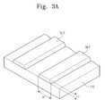
- FIGS. 3A and 3B illustrate a structure in which the thicknesses of the second and third clock interconnections are increased to reduce the delay time of the first and second clocks.
- FIG. 3A is a cut perspective view illustrating an exemplary embodiment of the second and third clock interconnections according to the present invention.
- the second and third clock interconnections SL 2 and SL 3 have a single layer structure including a first metal layer while being formed on the bottom substrate 110 .
- the first metal layer is used when the gate lines GL 1 to GLn and the gate electrode of the TFT Tr are formed on the bottom substrate 110 .
- the second and third clock interconnections SL 2 and SL 3 are substantially simultaneously formed through a process of forming the gate lines GL 1 to GLn and the gate electrode of the TFT Tr on the bottom substrate 110 .
- each of the second and third clock interconnections SL 2 and SL 3 may have a thickness of about 1500 ⁇ to about 3000 ⁇ .
- the widths w 1 of the second and third clock interconnections SL 2 and SL 3 may also be increased.
- FIG. 3B is a cut perspective view illustrating another exemplary embodiment of the second and third clock interconnections according to the present invention.
- each of the second and third clock interconnections SL 2 and SL 3 have a multi-layer structure.
- each of the second and third clock interconnections SL 2 and SL 3 has a structure, in which at least one layer is laminated.
- Each of the second and third interconnections SL 2 and SL 3 includes a first interconnection 111 and a second interconnection 112 formed on the first interconnection 111 .
- the first interconnection 111 may be substantially simultaneously formed through a process of forming the gate lines GL 1 to GLn and the gate electrode of the TFT Tr on the bottom substrate 110 .
- the second interconnection 112 may be substantially simultaneously formed through a process of forming the data lines DL 1 to DLm and the source/drain electrodes of the TFT Tr on the bottom substrate 110 .
- An insulating layer 113 is interposed between the first and second interconnections 111 and 112 .
- the insulating layer 113 is formed with one or more contact holes 113 a formed therethrough to expose the first interconnection 111 .
- the second interconnection 112 is electrically connected with the first interconnection 111 through the contact holes 113 a.
- each of the second and third clock interconnections SL 2 and SL 3 has the multi-layer structure, so that a resistance value of the second and third clock interconnections SL 2 and SL 3 is reduced.
- the delay time of the first and second clocks CKV and CKVB may be reduced so as to be less than about 2.0 ⁇ s.
- FIG. 4 is a circuit diagram of the exemplary last driving stage shown in FIG. 2 . Since the driving stages provided in the gate driver have the same internal circuit configuration, the last driving stage will be representatively described with reference to FIG. 4 .
- the last driving stage SRCn includes a pull-up unit 219 , a carry unit 220 , a pull-down unit 213 , a pull-up driver 214 , a ripple preventing unit 215 , a holding unit 216 , an inverter unit 217 and a reset unit 218 .
- the pull-up unit 219 includes a pull-up transistor NT 1 having a control electrode connected with an output terminal (hereinafter, referred to as a Q-node QN) of the pull-up driver 214 , an input electrode connected with the first clock terminal CK 1 , and an output electrode connected with the output terminal OUT.
- the pull-up transistor NT 1 pulls up the present gate signal output through the output terminal OUT to a high level of a clock (hereinafter, referred to as the first clock CKV as shown in FIG. 2 ) provided through the first clock terminal CK 1 in response to a voltage output from the pull-down unit 213 .
- the pull-up transistor NT 1 is turned on during a high interval (hereinafter, referred to as a first interval) of the first clock CK 1 of one frame, thereby maintaining the present gate signal in a high state during the first interval.
- the carry unit 220 includes a carry transistor NT 2 having a control electrode connected with the Q-node QN, an input electrode connected with the first clock terminal CK 1 , and an output electrode connected with the carry terminal CR.
- the carry transistor NT 2 pulls up the present gate signal, which is output through the carry terminal CR, to the high level of the first clock CKV in response to the voltage output from the pull-down unit 213 .
- the carry transistor NT 2 is turned on during the first interval of one frame to maintain the present carry signal in a high state during the first interval.
- the pull-down unit 213 includes a pull-down transistor NT 3 having a control electrode connected with the control terminal CT, an input electrode connected with the voltage input terminal Vin, and an output electrode connected with the output terminal OUT.
- the pull-down transistor NT 3 pulls down the pulled-up present gate signal to the gate off voltage V off (see FIG. 1 ), which is supplied through the voltage input terminal Vin, in response to the next gate signal.
- the pull-down transistor NT 3 is turned on by the next gate signal after the first interval to allow the present gate signal to be in a low state.
- the pull-up driver 214 includes a buffer transistor NT 4 , a first capacitor C 1 , a second capacitor C 2 and a discharge transistor NT 5 .
- the buffer transistor NT 4 includes an input electrode and a control electrode that are commonly connected with the input terminal IN, and an output electrode connected with the Q-node QN.
- the first capacitor C 1 is connected between the Q-node QN and the output terminal OUT, and the second capacitor C 2 is connected between the control electrode of the carry transistor NT 2 and the carry terminal CR.
- the discharge transistor NT 5 includes an input electrode connected with the output electrode of the buffer transistor NT 4 , a control electrode connected with the control terminal CT, and an output electrode connected with the voltage input terminal Vin.
- the buffer transistor NT 4 If the buffer transistor NT 4 is turned on in response to the previous carry signal, an electric potential of the Q-node QN increases, so that the pull-up transistor NT 1 and the carry transistor NT 2 are turned on. Then, if electric potentials of the output terminal OUT and the carry terminal CR increase by the pull-up transistor NT 1 and the carry transistor NT 2 which are turned on, the potential of the Q-node QN is boosted up by the first and second capacitors C 1 and C 2 . Thus, the pull-up transistor NT 1 and the carry transistor NT 2 are continuously turned on, so that the present gate and carry signals may be generated in a high state during the high interval of the first clock CKV.
- the ripple preventing unit 215 includes first to third ripple preventing transistors NT 6 to NT 8 to prevent the present gate signal and the carry signal from being rippled by the first clock CKV or the second clock CKVB during a second interval except for the first interval of one frame.
- the first ripple preventing transistor NT 6 includes a control electrode connected with the first clock terminal CK 1 , an input electrode connected with the output terminal OUT, and an output electrode connected with the Q-node QN.
- the second ripple preventing transistor NT 7 includes a control electrode connected with the second clock terminal CK 2 , an input electrode connected with the input terminal IN, and an output electrode connected with the Q-node QN.
- the third ripple preventing transistor NT 8 includes a control electrode connected with the second clock terminal CK 2 , an input electrode connected with the output terminal OUT, and an output electrode connected with the voltage input terminal Vin.
- the first ripple preventing transistor NT 6 provides the Q-node QN with the present gate signal in a low state, which is output from the output terminal OUT, in response to the first clock CKV.
- the electric potential of the Q-node QN is maintained in a low state in the high interval of the first clock CKV in the second interval, so that the first ripple preventing transistor NT 6 prevents the pull-up transistor NT 1 and the carry transistor NT 2 from being turned on during the high interval of the first clock CKV in the second interval.
- the second ripple preventing transistor NT 7 provides the Q-node QN with the previous carry signal in a low state, which is input through the input terminal IN, in response to a clock (hereinafter, referred to as the second clock CKVB as shown in FIG. 1 ) provided through the second clock terminal CK 2 .
- the electric potential of the Q-node QN is maintained in a low state in the high interval of the second clock CKVB in the second interval, so that the second ripple preventing transistor NT 7 prevents the pull-up transistor NT 1 and the carry transistor NT 2 from being turned on during the high interval of the second clock CKVB in the second interval.
- the present gate signal is discharged to the gate off voltage V off by the third ripple preventing transistor NT 8 when the second clock CKVB is supplied to the third ripple preventing transistor NT 8 .
- the present gate signal is maintained at the gate off voltage V off during the high interval of the second clock CKVB in the second interval.
- the holding unit 216 includes a holding transistor NT 9 having a control electrode connected with an output terminal of the inverter unit 217 , an input electrode connected with the voltage input terminal Vin, and an output electrode connected with the output terminal OUT.
- the inverter unit 217 includes first, second, third and fourth inverter transistors NT 10 , NT 11 , NT 12 and NT 13 , and third and fourth capacitors C 3 and C 4 to turn on or off the holding transistor NT 9 .
- the first inverter transistor NT 10 includes input and control electrodes commonly connected with the first clock terminal CK 1 , and an output electrode connected with an output electrode of the second inverter transistor NT 11 through the fourth capacitor C 4 .
- the second inverter transistor NT 11 includes an input electrode connected with the first clock terminal CK 1 , a control electrode connected with the input electrode through the third capacitor C 3 , and an output electrode connected with the output electrode of the holding transistor NT 9 .
- the third inverter transistor NT 12 includes an input electrode connected with the output electrode of the first inverter transistor NT 10 , a control electrode connected with the output terminal OUT, and an output electrode connected with the voltage input terminal Vin.
- the fourth inverter transistor NT 13 includes an input electrode connected with the control electrode of the holding transistor NT 9 , a control electrode connected with the output terminal OUT, and an output electrode connected with the voltage input terminal Vin.
- the third and fourth inverter transistors NT 12 and NT 13 are turned on in response to the present gate signal in a high state output through the output terminal OUT, the first clocks CKV output from the first and second inverter transistors NT 10 and NT 11 are discharged to the gate off voltage V off by the third and fourth inverter transistors NT 12 and NT 13 .
- the holding transistor NT 9 is turned off during the first interval in which the present gate signal is maintained in the high state.
- the present gate signal is transited to a low state in the second interval, the third and fourth inverter transistors NT 12 and NT 13 are turned off.
- the first clock CKV output from the first and second inverter transistors NT 10 and NT 11 are applied to the holding transistor NT 9 to turn on the holding transistor NT 9 .
- the present gate signal may be maintained in the gate off voltage V off by the holding transistor NT 9 during the high interval of the first clock CKV in the second interval.
- the reset unit 218 includes a reset transistor NT 14 having a control electrode connected with the reset terminal RE, an input electrode connected with the control electrode of the pull-up transistor NT 1 , and an output electrode connected with the voltage input terminal Vin.
- the electric potential of the Q-node is discharged to the gate off voltage V off by the reset transistor NT 14 when a signal is supplied to the reset transistor NT 14 from the output terminal OUT of the dummy stage DSRC (see FIG. 2 ) through the reset terminal RE.
- the pull-up transistor NT 1 and the carry transistor NT 2 are turned off in response to the reset signal of the dummy stage DSRC.
- the output signal of the dummy stage DSRC is provided to the reset terminals RE of the n driving stages SRC 1 to SRCn to turn off the pull-up transistor NT 1 and the carry transistor NT 1 and NT 2 provided in each driving stage, so that the n driving stages SRC 1 to SRCn may be reset.
- the transistors provided in the stages of the gate driver 210 include amorphous silicon (“a-Si”) transistors.
- the gate driver 210 As illustrated in FIG. 1 , after the gate driver 210 having the structure as described above is formed on the LCD panel 100 , the gate driver 210 is subject to an aging process (severe environment test) to change threshold voltage of the transistors provided in the stages.
- an aging process severe environment test
- FIG. 5 is a graph illustrating variation of the threshold voltage according to the aging process.
- an X-axis denotes a gate voltage Vg of a transistor and a Y-axis denotes a drain current ID of the transistor.
- a first graph G 1 denotes a threshold voltage Vth of the transistor before the aging process is performed and a second graph G 2 denotes the threshold voltage Vth of the transistor after the aging process is performed.
- the threshold voltage Vth of the transistor increases due to the temperature after the aging process is performed.
- the threshold voltage Vth of the transistor provided in each stage increases, thereby causing malfunction of each stage. As a result, an abnormal waveform may be output from the stages.
- the delay time of the first and second clocks CKV and CKVB supplied to the stages is reduced, a margin of the threshold voltage Vth increases, so that the stages may not malfunction. Accordingly, in the exemplary embodiments of the present invention, the delay time of the first and second clocks CKV and CKVB is reduced to be less than about 2.0 ⁇ s, so that the margin of the threshold voltage Vth can be increased more than 20V. Thus, the gate driver 210 may be prevented from malfunctioning in the high temperature aging process.
Landscapes
- Engineering & Computer Science (AREA)
- Physics & Mathematics (AREA)
- General Physics & Mathematics (AREA)
- Microelectronics & Electronic Packaging (AREA)
- Theoretical Computer Science (AREA)
- Chemical & Material Sciences (AREA)
- Crystallography & Structural Chemistry (AREA)
- Computer Hardware Design (AREA)
- Power Engineering (AREA)
- Nonlinear Science (AREA)
- Optics & Photonics (AREA)
- Mathematical Physics (AREA)
- Control Of Indicators Other Than Cathode Ray Tubes (AREA)
- Shift Register Type Memory (AREA)
Abstract
Description
Claims (14)
Applications Claiming Priority (2)
| Application Number | Priority Date | Filing Date | Title |
|---|---|---|---|
| KR10-2008-0070730 | 2008-07-21 | ||
| KR1020080070730A KR101556777B1 (en) | 2008-07-21 | 2008-07-21 | Display device |
Publications (2)
| Publication Number | Publication Date |
|---|---|
| US20100013823A1 US20100013823A1 (en) | 2010-01-21 |
| US9368084B2 true US9368084B2 (en) | 2016-06-14 |
Family
ID=41529931
Family Applications (1)
| Application Number | Title | Priority Date | Filing Date |
|---|---|---|---|
| US12/351,095 Active 2032-11-21 US9368084B2 (en) | 2008-07-21 | 2009-01-09 | Display apparatus and method thereof |
Country Status (2)
| Country | Link |
|---|---|
| US (1) | US9368084B2 (en) |
| KR (1) | KR101556777B1 (en) |
Families Citing this family (14)
| Publication number | Priority date | Publication date | Assignee | Title |
|---|---|---|---|---|
| TWI416530B (en) * | 2009-03-25 | 2013-11-21 | Wintek Corp | Shift register |
| KR101587610B1 (en) * | 2009-09-21 | 2016-01-25 | 삼성디스플레이 주식회사 | Drive circuit |
| KR101871993B1 (en) | 2011-08-23 | 2018-06-28 | 삼성디스플레이 주식회사 | Display device |
| KR20130097528A (en) * | 2012-02-24 | 2013-09-03 | 삼성디스플레이 주식회사 | 3d image display apparatus |
| CN103366704B (en) * | 2013-07-10 | 2015-08-19 | 京东方科技集团股份有限公司 | A kind of shift register cell and gate driver circuit, display device |
| KR20150070648A (en) * | 2013-12-17 | 2015-06-25 | 삼성디스플레이 주식회사 | Thin film transisotr |
| KR102187771B1 (en) * | 2014-03-13 | 2020-12-08 | 삼성디스플레이 주식회사 | Gate driver and display device including the same |
| JP6533065B2 (en) * | 2015-02-12 | 2019-06-19 | 株式会社ジャパンディスプレイ | Display device |
| CN104851383B (en) * | 2015-06-01 | 2017-08-11 | 京东方科技集团股份有限公司 | Shift register, gate driving circuit and display device |
| CN105245089B (en) * | 2015-11-06 | 2018-08-03 | 京东方科技集团股份有限公司 | Supplement reseting module, gate driving circuit and display device |
| CN110379347B (en) * | 2019-07-25 | 2023-01-24 | 云谷(固安)科技有限公司 | Screen body dummy device detection method and device |
| CN110706642B (en) * | 2019-11-08 | 2020-10-27 | 四川遂宁市利普芯微电子有限公司 | Oscillation circuit for LED display screen driving chip |
| KR102873258B1 (en) * | 2019-12-20 | 2025-10-21 | 삼성디스플레이 주식회사 | Display device |
| KR102330557B1 (en) | 2020-11-18 | 2021-11-24 | 주식회사 이지라이더 | Automatic rear door opening and closing apparatus of delivery truck |
Citations (6)
| Publication number | Priority date | Publication date | Assignee | Title |
|---|---|---|---|---|
| JPH1184427A (en) | 1997-09-11 | 1999-03-26 | Semiconductor Energy Lab Co Ltd | Drive circuit for liquid crystal display |
| KR20030080979A (en) | 2002-04-08 | 2003-10-17 | 삼성전자주식회사 | Liquid crystal display apparatus |
| US20050008114A1 (en) * | 2003-07-09 | 2005-01-13 | Seung-Hwan Moon | Shift register, scan driving circuit and display apparatus having the same |
| US20060066800A1 (en) * | 2004-09-28 | 2006-03-30 | Fujitsu Display Technologies Corporation | Liquid crystal display device |
| JP2006235437A (en) | 2005-02-28 | 2006-09-07 | Seiko Epson Corp | Electro-optical device, electronic apparatus, and method of manufacturing electro-optical device |
| US20070052656A1 (en) * | 2005-08-03 | 2007-03-08 | Samsung Electronics Co., Ltd. | Flat panel display and manufacturing method thereof |
-
2008
- 2008-07-21 KR KR1020080070730A patent/KR101556777B1/en active Active
-
2009
- 2009-01-09 US US12/351,095 patent/US9368084B2/en active Active
Patent Citations (6)
| Publication number | Priority date | Publication date | Assignee | Title |
|---|---|---|---|---|
| JPH1184427A (en) | 1997-09-11 | 1999-03-26 | Semiconductor Energy Lab Co Ltd | Drive circuit for liquid crystal display |
| KR20030080979A (en) | 2002-04-08 | 2003-10-17 | 삼성전자주식회사 | Liquid crystal display apparatus |
| US20050008114A1 (en) * | 2003-07-09 | 2005-01-13 | Seung-Hwan Moon | Shift register, scan driving circuit and display apparatus having the same |
| US20060066800A1 (en) * | 2004-09-28 | 2006-03-30 | Fujitsu Display Technologies Corporation | Liquid crystal display device |
| JP2006235437A (en) | 2005-02-28 | 2006-09-07 | Seiko Epson Corp | Electro-optical device, electronic apparatus, and method of manufacturing electro-optical device |
| US20070052656A1 (en) * | 2005-08-03 | 2007-03-08 | Samsung Electronics Co., Ltd. | Flat panel display and manufacturing method thereof |
Also Published As
| Publication number | Publication date |
|---|---|
| US20100013823A1 (en) | 2010-01-21 |
| KR20100009906A (en) | 2010-01-29 |
| KR101556777B1 (en) | 2015-10-06 |
Similar Documents
| Publication | Publication Date | Title |
|---|---|---|
| US9368084B2 (en) | Display apparatus and method thereof | |
| US9153190B2 (en) | Gate driver and display apparatus having the same | |
| US8264443B2 (en) | Ripple preventing gate driving circuit and display apparatus having the same | |
| US7899148B2 (en) | Shift register, scan driving circuit and display device having the same | |
| US8228282B2 (en) | Gate driving circuit, display apparatus having the same, and method thereof | |
| US7417458B2 (en) | Gate driving circuit and display apparatus having the same | |
| US8098227B2 (en) | Gate driving circuit and display apparatus having the same | |
| US9293093B2 (en) | Gate driver in which each stage thereof drives multiple gate lines and display apparatus having the same | |
| US8860648B2 (en) | Driving circuit with improved stability at high-temperature conditions | |
| KR101275248B1 (en) | Gate driver circuit and display apparatus having the same | |
| US9343030B2 (en) | Gate driving circuit and display apparatus including the same | |
| US8810498B2 (en) | Gate driving circuit and display apparatus having the same | |
| US8284149B2 (en) | Gate driving circuit and display device having the gate driving circuit | |
| US10777159B2 (en) | Gate driver and display apparatus having the same | |
| US9293090B2 (en) | Gate-driving apparatus and display device including the same | |
| US20100007635A1 (en) | Gate driver and display apparatus having the same | |
| US20130002309A1 (en) | Method of driving a gate line and gate drive circuit for performing the method | |
| US20060267912A1 (en) | Shift register and display device having the same, and method thereof | |
| US7408376B2 (en) | Array substrate | |
| US20080042950A1 (en) | Display substrate and display device having the same | |
| US9196213B2 (en) | Gate driving circuit and display device having the same | |
| KR101860732B1 (en) | Gate driving circuit and display device having the same | |
| US10923061B2 (en) | Gate driving circuit with reduced power consumption and display device including the same | |
| US9711654B2 (en) | Display device |
Legal Events
| Date | Code | Title | Description |
|---|---|---|---|
| AS | Assignment |
Owner name: SAMSUNG ELECTRONICS CO., LTD,KOREA, REPUBLIC OF Free format text: ASSIGNMENT OF ASSIGNORS INTEREST;ASSIGNORS:KWON, JI-HYUN;KWON, HO-KYOON;KI, DONG-HYON;AND OTHERS;REEL/FRAME:022083/0740 Effective date: 20081202 Owner name: SAMSUNG ELECTRONICS CO., LTD, KOREA, REPUBLIC OF Free format text: ASSIGNMENT OF ASSIGNORS INTEREST;ASSIGNORS:KWON, JI-HYUN;KWON, HO-KYOON;KI, DONG-HYON;AND OTHERS;REEL/FRAME:022083/0740 Effective date: 20081202 |
|
| AS | Assignment |
Owner name: SAMSUNG DISPLAY CO., LTD., KOREA, REPUBLIC OF Free format text: ASSIGNMENT OF ASSIGNORS INTEREST;ASSIGNOR:SAMSUNG ELECTRONICS CO., LTD.;REEL/FRAME:029093/0177 Effective date: 20120904 |
|
| FEPP | Fee payment procedure |
Free format text: PAYOR NUMBER ASSIGNED (ORIGINAL EVENT CODE: ASPN); ENTITY STATUS OF PATENT OWNER: LARGE ENTITY |
|
| STCF | Information on status: patent grant |
Free format text: PATENTED CASE |
|
| MAFP | Maintenance fee payment |
Free format text: PAYMENT OF MAINTENANCE FEE, 4TH YEAR, LARGE ENTITY (ORIGINAL EVENT CODE: M1551); ENTITY STATUS OF PATENT OWNER: LARGE ENTITY Year of fee payment: 4 |
|
| AS | Assignment |
Owner name: TCL CHINA STAR OPTOELECTRONICS TECHNOLOGY CO., LTD., CHINA Free format text: ASSIGNMENT OF ASSIGNORS INTEREST;ASSIGNOR:SAMSUNG DISPLAY CO., LTD.;REEL/FRAME:060778/0487 Effective date: 20220602 |
|
| MAFP | Maintenance fee payment |
Free format text: PAYMENT OF MAINTENANCE FEE, 8TH YEAR, LARGE ENTITY (ORIGINAL EVENT CODE: M1552); ENTITY STATUS OF PATENT OWNER: LARGE ENTITY Year of fee payment: 8 |