US9341896B2 - Liquid crystal display - Google Patents

Liquid crystal display Download PDF

Info

Publication number
US9341896B2
US9341896B2 US13/599,414 US201213599414A US9341896B2 US 9341896 B2 US9341896 B2 US 9341896B2 US 201213599414 A US201213599414 A US 201213599414A US 9341896 B2 US9341896 B2 US 9341896B2
Authority
US
United States
Prior art keywords
liquid crystal
electrode
gate
display panel
lcd
Prior art date
Legal status (The legal status is an assumption and is not a legal conclusion. Google has not performed a legal analysis and makes no representation as to the accuracy of the status listed.)
Expired - Fee Related, expires
Application number
US13/599,414
Other versions
US20120320294A1 (en
Inventor
Dong-Gyu Kim
Kyoung-Ju Shin
Jong-Ho Son
Jun-Pyo Lee
Seung-Soo Baek
Current Assignee (The listed assignees may be inaccurate. Google has not performed a legal analysis and makes no representation or warranty as to the accuracy of the list.)
Samsung Display Co Ltd
Original Assignee
Samsung Display Co Ltd
Priority date (The priority date is an assumption and is not a legal conclusion. Google has not performed a legal analysis and makes no representation as to the accuracy of the date listed.)
Filing date
Publication date
Priority claimed from KR1020080006346A external-priority patent/KR101443856B1/en
Application filed by Samsung Display Co Ltd filed Critical Samsung Display Co Ltd
Priority to US13/599,414 priority Critical patent/US9341896B2/en
Assigned to SAMSUNG DISPLAY CO., LTD. reassignment SAMSUNG DISPLAY CO., LTD. ASSIGNMENT OF ASSIGNORS INTEREST (SEE DOCUMENT FOR DETAILS). Assignors: BAEK, SEUNG-SOO, KIM, DONG-GYU, LEE, JUN-PYO, SHIN, KYOUNG-JU, SON, JONG-HO
Publication of US20120320294A1 publication Critical patent/US20120320294A1/en
Application granted granted Critical
Publication of US9341896B2 publication Critical patent/US9341896B2/en
Expired - Fee Related legal-status Critical Current
Adjusted expiration legal-status Critical

Links

Images

Classifications

    • GPHYSICS
    • G02OPTICS
    • G02FOPTICAL DEVICES OR ARRANGEMENTS FOR THE CONTROL OF LIGHT BY MODIFICATION OF THE OPTICAL PROPERTIES OF THE MEDIA OF THE ELEMENTS INVOLVED THEREIN; NON-LINEAR OPTICS; FREQUENCY-CHANGING OF LIGHT; OPTICAL LOGIC ELEMENTS; OPTICAL ANALOGUE/DIGITAL CONVERTERS
    • G02F1/00Devices or arrangements for the control of the intensity, colour, phase, polarisation or direction of light arriving from an independent light source, e.g. switching, gating or modulating; Non-linear optics
    • G02F1/01Devices or arrangements for the control of the intensity, colour, phase, polarisation or direction of light arriving from an independent light source, e.g. switching, gating or modulating; Non-linear optics for the control of the intensity, phase, polarisation or colour 
    • G02F1/13Devices or arrangements for the control of the intensity, colour, phase, polarisation or direction of light arriving from an independent light source, e.g. switching, gating or modulating; Non-linear optics for the control of the intensity, phase, polarisation or colour  based on liquid crystals, e.g. single liquid crystal display cells
    • G02F1/133Constructional arrangements; Operation of liquid crystal cells; Circuit arrangements
    • G02F1/1333Constructional arrangements; Manufacturing methods
    • G02F1/1337Surface-induced orientation of the liquid crystal molecules, e.g. by alignment layers
    • G02F1/133707Structures for producing distorted electric fields, e.g. bumps, protrusions, recesses, slits in pixel electrodes
    • CCHEMISTRY; METALLURGY
    • C09DYES; PAINTS; POLISHES; NATURAL RESINS; ADHESIVES; COMPOSITIONS NOT OTHERWISE PROVIDED FOR; APPLICATIONS OF MATERIALS NOT OTHERWISE PROVIDED FOR
    • C09KMATERIALS FOR MISCELLANEOUS APPLICATIONS, NOT PROVIDED FOR ELSEWHERE
    • C09K19/00Liquid crystal materials
    • C09K19/02Liquid crystal materials characterised by optical, electrical or physical properties of the components, in general
    • CCHEMISTRY; METALLURGY
    • C09DYES; PAINTS; POLISHES; NATURAL RESINS; ADHESIVES; COMPOSITIONS NOT OTHERWISE PROVIDED FOR; APPLICATIONS OF MATERIALS NOT OTHERWISE PROVIDED FOR
    • C09KMATERIALS FOR MISCELLANEOUS APPLICATIONS, NOT PROVIDED FOR ELSEWHERE
    • C09K19/00Liquid crystal materials
    • C09K19/04Liquid crystal materials characterised by the chemical structure of the liquid crystal components, e.g. by a specific unit
    • C09K2019/0444Liquid crystal materials characterised by the chemical structure of the liquid crystal components, e.g. by a specific unit characterized by a linking chain between rings or ring systems, a bridging chain between extensive mesogenic moieties or an end chain group
    • GPHYSICS
    • G02OPTICS
    • G02FOPTICAL DEVICES OR ARRANGEMENTS FOR THE CONTROL OF LIGHT BY MODIFICATION OF THE OPTICAL PROPERTIES OF THE MEDIA OF THE ELEMENTS INVOLVED THEREIN; NON-LINEAR OPTICS; FREQUENCY-CHANGING OF LIGHT; OPTICAL LOGIC ELEMENTS; OPTICAL ANALOGUE/DIGITAL CONVERTERS
    • G02F1/00Devices or arrangements for the control of the intensity, colour, phase, polarisation or direction of light arriving from an independent light source, e.g. switching, gating or modulating; Non-linear optics
    • G02F1/01Devices or arrangements for the control of the intensity, colour, phase, polarisation or direction of light arriving from an independent light source, e.g. switching, gating or modulating; Non-linear optics for the control of the intensity, phase, polarisation or colour 
    • G02F1/13Devices or arrangements for the control of the intensity, colour, phase, polarisation or direction of light arriving from an independent light source, e.g. switching, gating or modulating; Non-linear optics for the control of the intensity, phase, polarisation or colour  based on liquid crystals, e.g. single liquid crystal display cells
    • G02F1/133Constructional arrangements; Operation of liquid crystal cells; Circuit arrangements
    • G02F1/136Liquid crystal cells structurally associated with a semi-conducting layer or substrate, e.g. cells forming part of an integrated circuit
    • G02F1/1362Active matrix addressed cells
    • G02F1/136209Light shielding layers, e.g. black matrix, incorporated in the active matrix substrate, e.g. structurally associated with the switching element
    • GPHYSICS
    • G02OPTICS
    • G02FOPTICAL DEVICES OR ARRANGEMENTS FOR THE CONTROL OF LIGHT BY MODIFICATION OF THE OPTICAL PROPERTIES OF THE MEDIA OF THE ELEMENTS INVOLVED THEREIN; NON-LINEAR OPTICS; FREQUENCY-CHANGING OF LIGHT; OPTICAL LOGIC ELEMENTS; OPTICAL ANALOGUE/DIGITAL CONVERTERS
    • G02F1/00Devices or arrangements for the control of the intensity, colour, phase, polarisation or direction of light arriving from an independent light source, e.g. switching, gating or modulating; Non-linear optics
    • G02F1/01Devices or arrangements for the control of the intensity, colour, phase, polarisation or direction of light arriving from an independent light source, e.g. switching, gating or modulating; Non-linear optics for the control of the intensity, phase, polarisation or colour 
    • G02F1/13Devices or arrangements for the control of the intensity, colour, phase, polarisation or direction of light arriving from an independent light source, e.g. switching, gating or modulating; Non-linear optics for the control of the intensity, phase, polarisation or colour  based on liquid crystals, e.g. single liquid crystal display cells
    • G02F1/133Constructional arrangements; Operation of liquid crystal cells; Circuit arrangements
    • G02F1/136Liquid crystal cells structurally associated with a semi-conducting layer or substrate, e.g. cells forming part of an integrated circuit
    • G02F1/1362Active matrix addressed cells
    • G02F1/136213Storage capacitors associated with the pixel electrode
    • GPHYSICS
    • G02OPTICS
    • G02FOPTICAL DEVICES OR ARRANGEMENTS FOR THE CONTROL OF LIGHT BY MODIFICATION OF THE OPTICAL PROPERTIES OF THE MEDIA OF THE ELEMENTS INVOLVED THEREIN; NON-LINEAR OPTICS; FREQUENCY-CHANGING OF LIGHT; OPTICAL LOGIC ELEMENTS; OPTICAL ANALOGUE/DIGITAL CONVERTERS
    • G02F1/00Devices or arrangements for the control of the intensity, colour, phase, polarisation or direction of light arriving from an independent light source, e.g. switching, gating or modulating; Non-linear optics
    • G02F1/01Devices or arrangements for the control of the intensity, colour, phase, polarisation or direction of light arriving from an independent light source, e.g. switching, gating or modulating; Non-linear optics for the control of the intensity, phase, polarisation or colour 
    • G02F1/13Devices or arrangements for the control of the intensity, colour, phase, polarisation or direction of light arriving from an independent light source, e.g. switching, gating or modulating; Non-linear optics for the control of the intensity, phase, polarisation or colour  based on liquid crystals, e.g. single liquid crystal display cells
    • G02F1/133Constructional arrangements; Operation of liquid crystal cells; Circuit arrangements
    • G02F1/136Liquid crystal cells structurally associated with a semi-conducting layer or substrate, e.g. cells forming part of an integrated circuit
    • G02F1/1362Active matrix addressed cells
    • G02F1/13624Active matrix addressed cells having more than one switching element per pixel
    • GPHYSICS
    • G02OPTICS
    • G02FOPTICAL DEVICES OR ARRANGEMENTS FOR THE CONTROL OF LIGHT BY MODIFICATION OF THE OPTICAL PROPERTIES OF THE MEDIA OF THE ELEMENTS INVOLVED THEREIN; NON-LINEAR OPTICS; FREQUENCY-CHANGING OF LIGHT; OPTICAL LOGIC ELEMENTS; OPTICAL ANALOGUE/DIGITAL CONVERTERS
    • G02F1/00Devices or arrangements for the control of the intensity, colour, phase, polarisation or direction of light arriving from an independent light source, e.g. switching, gating or modulating; Non-linear optics
    • G02F1/01Devices or arrangements for the control of the intensity, colour, phase, polarisation or direction of light arriving from an independent light source, e.g. switching, gating or modulating; Non-linear optics for the control of the intensity, phase, polarisation or colour 
    • G02F1/13Devices or arrangements for the control of the intensity, colour, phase, polarisation or direction of light arriving from an independent light source, e.g. switching, gating or modulating; Non-linear optics for the control of the intensity, phase, polarisation or colour  based on liquid crystals, e.g. single liquid crystal display cells
    • G02F1/133Constructional arrangements; Operation of liquid crystal cells; Circuit arrangements
    • G02F1/136Liquid crystal cells structurally associated with a semi-conducting layer or substrate, e.g. cells forming part of an integrated circuit
    • G02F1/1362Active matrix addressed cells
    • G02F1/136286Wiring, e.g. gate line, drain line
    • GPHYSICS
    • G02OPTICS
    • G02FOPTICAL DEVICES OR ARRANGEMENTS FOR THE CONTROL OF LIGHT BY MODIFICATION OF THE OPTICAL PROPERTIES OF THE MEDIA OF THE ELEMENTS INVOLVED THEREIN; NON-LINEAR OPTICS; FREQUENCY-CHANGING OF LIGHT; OPTICAL LOGIC ELEMENTS; OPTICAL ANALOGUE/DIGITAL CONVERTERS
    • G02F1/00Devices or arrangements for the control of the intensity, colour, phase, polarisation or direction of light arriving from an independent light source, e.g. switching, gating or modulating; Non-linear optics
    • G02F1/01Devices or arrangements for the control of the intensity, colour, phase, polarisation or direction of light arriving from an independent light source, e.g. switching, gating or modulating; Non-linear optics for the control of the intensity, phase, polarisation or colour 
    • G02F1/13Devices or arrangements for the control of the intensity, colour, phase, polarisation or direction of light arriving from an independent light source, e.g. switching, gating or modulating; Non-linear optics for the control of the intensity, phase, polarisation or colour  based on liquid crystals, e.g. single liquid crystal display cells
    • G02F1/137Devices or arrangements for the control of the intensity, colour, phase, polarisation or direction of light arriving from an independent light source, e.g. switching, gating or modulating; Non-linear optics for the control of the intensity, phase, polarisation or colour  based on liquid crystals, e.g. single liquid crystal display cells characterised by the electro-optical or magneto-optical effect, e.g. field-induced phase transition, orientation effect, guest-host interaction or dynamic scattering
    • GPHYSICS
    • G02OPTICS
    • G02FOPTICAL DEVICES OR ARRANGEMENTS FOR THE CONTROL OF LIGHT BY MODIFICATION OF THE OPTICAL PROPERTIES OF THE MEDIA OF THE ELEMENTS INVOLVED THEREIN; NON-LINEAR OPTICS; FREQUENCY-CHANGING OF LIGHT; OPTICAL LOGIC ELEMENTS; OPTICAL ANALOGUE/DIGITAL CONVERTERS
    • G02F2201/00Constructional arrangements not provided for in groups G02F1/00 - G02F7/00
    • G02F2201/40Arrangements for improving the aperture ratio
    • GPHYSICS
    • G09EDUCATION; CRYPTOGRAPHY; DISPLAY; ADVERTISING; SEALS
    • G09GARRANGEMENTS OR CIRCUITS FOR CONTROL OF INDICATING DEVICES USING STATIC MEANS TO PRESENT VARIABLE INFORMATION
    • G09G2300/00Aspects of the constitution of display devices
    • G09G2300/04Structural and physical details of display devices
    • G09G2300/0421Structural details of the set of electrodes
    • G09G2300/0426Layout of electrodes and connections
    • GPHYSICS
    • G09EDUCATION; CRYPTOGRAPHY; DISPLAY; ADVERTISING; SEALS
    • G09GARRANGEMENTS OR CIRCUITS FOR CONTROL OF INDICATING DEVICES USING STATIC MEANS TO PRESENT VARIABLE INFORMATION
    • G09G3/00Control arrangements or circuits, of interest only in connection with visual indicators other than cathode-ray tubes
    • G09G3/20Control arrangements or circuits, of interest only in connection with visual indicators other than cathode-ray tubes for presentation of an assembly of a number of characters, e.g. a page, by composing the assembly by combination of individual elements arranged in a matrix no fixed position being assigned to or needed to be assigned to the individual characters or partial characters
    • G09G3/34Control arrangements or circuits, of interest only in connection with visual indicators other than cathode-ray tubes for presentation of an assembly of a number of characters, e.g. a page, by composing the assembly by combination of individual elements arranged in a matrix no fixed position being assigned to or needed to be assigned to the individual characters or partial characters by control of light from an independent source
    • G09G3/36Control arrangements or circuits, of interest only in connection with visual indicators other than cathode-ray tubes for presentation of an assembly of a number of characters, e.g. a page, by composing the assembly by combination of individual elements arranged in a matrix no fixed position being assigned to or needed to be assigned to the individual characters or partial characters by control of light from an independent source using liquid crystals
    • G09G3/3607Control arrangements or circuits, of interest only in connection with visual indicators other than cathode-ray tubes for presentation of an assembly of a number of characters, e.g. a page, by composing the assembly by combination of individual elements arranged in a matrix no fixed position being assigned to or needed to be assigned to the individual characters or partial characters by control of light from an independent source using liquid crystals for displaying colours or for displaying grey scales with a specific pixel layout, e.g. using sub-pixels
    • GPHYSICS
    • G09EDUCATION; CRYPTOGRAPHY; DISPLAY; ADVERTISING; SEALS
    • G09GARRANGEMENTS OR CIRCUITS FOR CONTROL OF INDICATING DEVICES USING STATIC MEANS TO PRESENT VARIABLE INFORMATION
    • G09G3/00Control arrangements or circuits, of interest only in connection with visual indicators other than cathode-ray tubes
    • G09G3/20Control arrangements or circuits, of interest only in connection with visual indicators other than cathode-ray tubes for presentation of an assembly of a number of characters, e.g. a page, by composing the assembly by combination of individual elements arranged in a matrix no fixed position being assigned to or needed to be assigned to the individual characters or partial characters
    • G09G3/34Control arrangements or circuits, of interest only in connection with visual indicators other than cathode-ray tubes for presentation of an assembly of a number of characters, e.g. a page, by composing the assembly by combination of individual elements arranged in a matrix no fixed position being assigned to or needed to be assigned to the individual characters or partial characters by control of light from an independent source
    • G09G3/36Control arrangements or circuits, of interest only in connection with visual indicators other than cathode-ray tubes for presentation of an assembly of a number of characters, e.g. a page, by composing the assembly by combination of individual elements arranged in a matrix no fixed position being assigned to or needed to be assigned to the individual characters or partial characters by control of light from an independent source using liquid crystals
    • G09G3/3611Control of matrices with row and column drivers
    • G09G3/3648Control of matrices with row and column drivers using an active matrix
    • G09G3/3659Control of matrices with row and column drivers using an active matrix the addressing of the pixel involving the control of two or more scan electrodes or two or more data electrodes, e.g. pixel voltage dependant on signal of two data electrodes

Definitions

  • Exemplary embodiments of the present invention relate to a liquid crystal display (LCD) that may provide an increased aperture ratio by negating the need for storage wiring.
  • LCD liquid crystal display
  • FPDs flat panel displays
  • PDPs plasma display panels
  • PLCs plasma address liquid crystal display panels
  • LCDs liquid crystal displays
  • OLEDs organic light emitting diodes
  • LCDs are one of the most widely used FPDs.
  • An LCD includes two substrates on which electrodes are disposed, and a liquid crystal layer disposed between the two substrates.
  • the alignment of liquid crystals of the liquid crystal layer is altered when voltages are applied to the electrodes, thereby adjusting the light transmissivity of the LCD. In this way, the LCD displays a desired image.
  • a signal transmitted to a pixel electrode to alter the alignment of the liquid crystal must be maintained for a certain period of time.
  • a signal transmitted to the pixel electrode to alter the alignment of the liquid crystals leaks within a short period of time.
  • storage capacitors are connected in parallel to the pixel electrode so that electric charges applied to the liquid crystals may be maintained for the necessary period of time.
  • the pixel aperture ratio of the LCD may be reduced.
  • the present invention provide a liquid crystal display (LCD) that may increase an aperture ratio by negating the need for storage wiring and improve display quality.
  • LCD liquid crystal display
  • the present invention discloses an LCD comprising: a liquid crystal panel, and a gate driver which applies a gate signal having a driving frequency equal to or greater than 100 Hz to the liquid crystal panel, wherein the liquid crystal panel comprises: a first display panel, a second display panel facing the first display panel, and a liquid crystal composition disposed between the first display panel and the second display panel and includes liquid crystals.
  • a dielectric constant in a direction parallel to a long axis of the liquid crystals is defined as a horizontal dielectric constant ⁇
  • a dielectric constant in a direction perpendicular to the long axis of the liquid crystals is defined as a vertical dielectric constant ⁇
  • the difference between the vertical dielectric constant ⁇ and the horizontal dielectric constant ⁇ is defined as a dielectric anisotropy ⁇
  • a ratio ⁇ / ⁇ of the dielectric anisotropy ⁇ to the vertical dielectric constant ⁇ of the liquid crystal composition is 0.5 or less.
  • the present invention also discloses an LCD comprising a liquid crystal panel, and a gate driver which applies a gate signal having a driving frequency equal to or greater than 100 Hz to the liquid crystal panel, wherein the liquid crystal panel comprises a first display panel, a pixel electrode disposed on the first display panel, a second display panel facing the first display panel, a common electrode disposed on the second display panel and overlaps the pixel electrode, a decoupling electrode that partially overlaps the pixel electrode, and a liquid crystal composition disposed between the first display panel and the second display panel and includes liquid crystals.
  • a dielectric constant in a direction parallel to a long axis of the liquid crystals is defined as a horizontal dielectric constant ⁇
  • a dielectric constant in a direction perpendicular to the long axis of the liquid crystals is defined as a vertical dielectric constant ⁇
  • the difference between the vertical dielectric constant ⁇ and the horizontal dielectric constant ⁇ is defined as dielectric anisotropy ⁇
  • a ratio ⁇ / ⁇ of the dielectric anisotropy ⁇ to the vertical dielectric constant ⁇ of the liquid crystal composition is 0.5 or less
  • capacitance between the pixel electrode and the decoupling electrode is 5 to 20% of capacitance between the common electrode and the pixel electrode.
  • FIG. 1 is a block diagram of a liquid crystal display (LCD) according to an exemplary embodiment of the present invention.
  • LCD liquid crystal display
  • FIG. 2 is at plan view of a liquid crystal panel according to the exemplary embodiment of the present invention.
  • FIG. 3 is a cross-sectional view of the liquid crystal panel taken along line III-III′ of FIG. 2 .
  • FIG. 4 is a plan view of a lower display panel included in a liquid crystal panel according to another exemplary embodiment of the present invention.
  • FIG. 5 is a plan view of an upper display panel included in the liquid crystal panel according to another exemplary embodiment of the present invention.
  • FIG. 6 is a plan view of the liquid crystal panel according to another exemplary embodiment of the present invention.
  • FIG. 7 is a cross-sectional view of the liquid crystal panel of FIG. 6 taken along line VII-VII′.
  • FIG. 8 is an equivalent circuit diagram of a pixel included in the liquid crystal panel of FIG. 6 .
  • FIG. 9 is a plan view of a lower display panel included in a liquid crystal panel according to still another exemplary embodiment of the present invention.
  • FIG. 10 is a plan view of a lower display panel included in a liquid crystal panel according to still another exemplary embodiment of the present invention.
  • FIG. 11 is a plan view of a lower display panel included in a liquid crystal panel according to still another exemplary embodiment of the present invention.
  • FIG. 12 is a plan view of a lower display panel included in a liquid crystal panel according to still another exemplary embodiment of the present invention.
  • FIG. 1 is a block diagram of a liquid crystal display (LCD) according to an exemplary embodiment of the present invention.
  • the LCD includes a liquid crystal panel 500 , a timing controller 600 , a data driver 700 and a gate driver 800 .
  • the timing controller 600 may control the data driver 700 and the gate driver 800 to display a desired image on the liquid crystal panel 500 .
  • the timing controller 600 may generate a data control signal (DCS) for controlling the data driver 700 and transmit the data control signal (DCS) to the data driver 700 .
  • the timing controller 600 may generate a gate control signal (GCS) for controlling the gate driver 800 and transmit the gate control signal (GCS) to the gate driver 800 .
  • the timing controller 600 may generate the data control signal (DCS) and the gate control signal (GCS) to correspond to a driving frequency of the LCD.
  • the driving frequency of the LCD may be the number of frames being displayed per second on the liquid crystal panel.
  • the driving frequency of the LCD may be the number of times a data voltage is applied to each pixel electrode per second in the LCD.
  • the driving frequency of a high frequency may mean the driving frequency equal to or greater than 100 Hz.
  • the timing controller 600 may generate the data control signal (DCS) and the gate control signal (GCS) to correspond to the driving frequency of a high frequency. In some exemplary embodiments, the timing controller 600 may generate the data control signal (DCS) and the gate control signal (GCS) corresponding to the driving frequency equal to or greater than 100 Hz. In some other exemplary embodiments, the timing controller 600 may generate the data control signal (DCS) and the gate control signal (GCS) corresponding to the driving frequency of 120 Hz, 180 Hz, 240 Hz or the like, which is a multiple of 60 Hz.
  • the data driver 700 may receive the data control signal (DCS) from the timing controller 600 , generate data signals D 1 , D 2 , . . . , Dm, and apply the data signals D 1 , D 2 , . . . , Dm to the liquid crystal panel 500 .
  • the data signals D 1 , D 2 , . . . , Dm may include information regarding colors and grayscales to be displayed by pixels included in the liquid crystal panel 500 .
  • the data driver 700 may generate the data signals D 1 , D 2 , . . . , Dm to correspond to the driving frequency of a high frequency. In some exemplary embodiments, the data driver 700 may generate the data signals D 1 , D 2 , . . .
  • the data driver 700 may generate the data signals D 1 , D 2 , . . . , Dm corresponding to the driving frequency of 120 Hz, 180 Hz, 240 Hz or the like, which are all multiples of 60 Hz.
  • the gate driver 800 may receive the gate control signal (GCS) and generate gate signals G 1 , G 2 , . . . , Gn corresponding to the gate control signal (GCS).
  • the gate signals G 1 , G 2 , . . . , Gn may control whether the respective pixels included in the liquid crystal panel 500 receive the data signals D 1 , D 2 , . . . , Dm.
  • the gate driver 800 may generate the gate signals G 1 , G 2 , . . . , Gn to correspond to the driving frequency of a high frequency.
  • the gate driver 800 may generate the gate signals G 1 , G 2 , . . . , Gn corresponding to the driving frequency equal to or greater than 100 Hz.
  • the gate driver 800 may generate the gate signals G 1 , G 2 , . . . , Gn corresponding to the driving frequency of 120 Hz, 180 Hz, 240 Hz or the like, which are all multiples of 60 Hz.
  • the frequency of the gate signals may be equal to the driving frequency.
  • the driving frequency is a high frequency, because the interval at which the data voltage is applied to the pixel electrode is small, although there is no storage capacitor or the value of the storage capacitor is very small, a reduction in the magnitude of the data voltage applied to the pixel electrode is small, thereby maintaining display quality. Accordingly, if the driving frequency is a high frequency, when a storage wiring is formed to be small or omitted, it is possible to maintain display quality while increasing an aperture ratio.
  • FIG. 2 is a plan view of the liquid crystal panel according to an exemplary embodiment of the present invention.
  • FIG. 3 is a cross-sectional view of the liquid crystal panel taken along a line III-III′ of FIG. 2 .
  • a gate line 22 is disposed on a first insulating substrate 10 , which may be made of transparent glass.
  • the gate line 22 generally extends in a horizontal direction and delivers a gate signal Ga (a is an integer equal to or greater than 1 and equal to or smaller than n, 1 ⁇ a ⁇ n).
  • Ga is an integer equal to or greater than 1 and equal to or smaller than n, 1 ⁇ a ⁇ n.
  • the gate line 22 is allocated to each pixel.
  • the gate line 22 has a protruding gate electrode 26 .
  • the gate line 22 and the gate electrode 26 are collectively referred to as gate wiring.
  • the gate wiring may be made of aluminum (Al)-based metal such as Al or Al alloys, silver (Ag)-based metal such as Ag or Ag alloys, copper (Cu)-based metal such as Cu or Cu alloys, molybdenum (Mo)-based metal such as Mo or Mo alloys, chrome (Cr), titanium (Ti), or tantalum (Ta).
  • the gate wiring may have a multi-layer structure composed of two conductive layers (not shown) having different physical characteristics.
  • one of the two conductive layers may be made of metal with low resistivity, such as Al-based metal, Ag-based metal or Cu-based metal, in order to reduce a signal delay or a voltage drop of the gate wiring.
  • the other one of the conductive layers may be made of a different material, in particular, a material having superior contact characteristics with indium tin oxide (ITO) and indium zinc oxide (IZO), such as Mo-based metal, Cr, Ti, or Ta.
  • ITO indium tin oxide
  • IZO indium zinc oxide
  • Examples of the multi-layer structure include a combination of a Cr lower layer and an Al upper layer and a combination of an Al lower layer and a Mo upper layer.
  • the present invention is not limited thereto.
  • the gate wiring may be made of various metals and conductors.
  • a gate insulating film 30 which may be made of silicon nitride (SiNx), is disposed on the gate line 22 and gate electrode 26 .
  • a semiconductor layer 40 which may be made of hydrogenated amorphous silicon or polycrystalline silicon, is disposed on the gate insulating film 30 .
  • the semiconductor layer 40 may have various shapes.
  • the semiconductor layer 40 may be shaped like an island or may be linear.
  • the semiconductor layer 40 is shaped like an island.
  • Ohmic contact layers 55 and 56 may be made of a material, such as silicide or n+ hydrogenated amorphous silicon which is doped with n-type impurities in high concentration, and are disposed on the semiconductor layer 40 .
  • the ohmic contact layers 55 and 56 are arranged in pairs on the semiconductor layer 40 .
  • a data line 62 and a drain electrode 66 which corresponds to the data line 62 , are disposed on the ohmic contact layers 55 and 56 and the gate insulating film 30 .
  • the data line 62 generally extends in a vertical direction to cross the gate line 22 and delivers a data signal Db (b is an integer equal to or greater than 1 and equal to or smaller than m, 1 ⁇ b ⁇ m).
  • a source electrode 65 extends from the data line 62 toward the drain electrode 66 .
  • the data line 62 delivers the data signal Db to a pixel electrode 82 .
  • the data line 62 , the source electrode 65 , and the drain electrode 66 are collectively referred to as the data wiring.
  • the data wiring may be made of Cr, Mo-based metal, or refractory metal such as Ta and Ti.
  • the data wiring may have a multi-layer structure composed of a lower layer (not shown), which is made of refractory metal, and an upper layer (not shown) which is made of a material with low resistivity and disposed on the lower layer.
  • examples of the multi-layer structure may include a combination of a Cr lower layer and an Al upper layer and a combination of an Al lower layer and a Mo upper layer.
  • the multi-layer structure may be a triple-layer structure having Mo—Al—Mo layers.
  • the source electrode 65 at least partially overlaps the semiconductor layer 40 .
  • the drain electrode 66 faces the source electrode 65 on the gate electrode 26 and at least partially overlaps the semiconductor layer 40 .
  • the ohmic contact layers 55 and 56 described above are interposed between the semiconductor layer 40 , which is disposed under the ohmic contact layers 55 and 56 , and the source electrode 65 and the drain electrode 66 which are disposed on the ohmic contact layers 55 and 56 , respectively.
  • the ohmic contact layers 55 and 56 may reduce contact resistance between the semiconductor layer 40 and the source and drain electrodes 65 and 66 , respectively.
  • a passivation layer 70 is disposed on the data wiring and an exposed portion of the semiconductor layer 40 .
  • the passivation layer 70 may be made of an inorganic material such as silicon nitride (SiN x ) or silicon oxide (SiO x ), an organic material having photosensitivity and superior planarization characteristics, or a low-k dielectric material formed by plasma enhanced chemical vapor deposition (PECVD), such as a-Si:C:O or a-Si:O:F.
  • PECVD plasma enhanced chemical vapor deposition
  • the passivation layer 70 may be composed of a lower inorganic layer and an upper organic layer in order to protect the exposed portion of the semiconductor layer 40 while taking advantage of the superior characteristics of an organic layer.
  • a red (R), green (G) or blue (B) color filter may be used as the passivation layer 70 .
  • a contact hole 76 is formed in the passivation layer 70 .
  • the pixel electrode 82 is connected to the drain electrode 66 through the contact hole 76 . Therefore, the pixel electrode 82 receives a data voltage and a control voltage from the drain electrode 66 .
  • the pixel electrode 82 to which the data voltage is applied, generates an electric field together with a common electrode 91 of an upper display panel 200 , thereby determining the alignment of liquid crystal between the pixel electrode 82 and the common electrode 91 .
  • An alignment film (not shown), which can align a liquid crystal layer 300 , may be coated on the pixel electrode 82 and the passivation layer 70 .
  • a black matrix 94 to prevent the leakage of light and define a pixel region is disposed on a second insulating substrate 90 which may be made of transparent glass.
  • the black matrix 94 may be disposed on portions of the second insulating substrate 90 , which correspond to the gate line 22 and the data line 62 , and a portion of the second insulating substrate 90 which corresponds to a thin-film transistor (TFT).
  • TFT thin-film transistor
  • the black matrix 94 may have various shapes in order to prevent the leakage of light in the vicinity of the pixel electrode 82 and the TFT.
  • the black matrix 94 may be made of metal (metal oxide), such as chrome or chrome oxide, or organic black resist.
  • R, G and B color filters 92 may be sequentially arranged in the pixel region between the black matrices 94 .
  • An overcoat layer 95 may be formed on the R, G and B color filters 92 to planarize their step heights.
  • the common electrode 91 may be made of a transparent conductive material, such as ITO or IZO, and disposed on the overcoat layer 95 .
  • the common electrode 91 faces the pixel electrode 82 , and the liquid crystal layer 300 is disposed between the common electrode 91 and the pixel electrode 82 .
  • An alignment film (not shown) to align the liquid crystal may be coated on the common electrode 91 .
  • the liquid crystal panel may further include a storage wiring for forming a storage capacitor.
  • the storage wiring forms the storage capacitor to reduce a decreasing rate of the magnitude of the data voltage applied to the pixel electrode 82 , thereby improving display quality.
  • the driving frequency of the LCD is a high frequency
  • the interval at which the data voltage is applied to the pixel electrode 82 becomes small. Accordingly, although the storage wiring is omitted, a reduction in the magnitude of the data voltage applied to the pixel electrode 82 is small, and the display quality is not reduced compared to a case of including the storage wiring. Omission of the storage wiring makes it possible to improve an aperture ratio of the LCD.
  • a liquid crystal molecule When a liquid crystal molecule is an optically uniaxial crystal, it exhibits anisotropy ⁇ n of a refractive index. That is, a uniaxial crystal molecule exhibits a refractive index n e for ordinary light, in which an electric vector of a light wave oscillates perpendicular to a plane on which an optical axis lies, and a refractive index n o for extraordinary light in which an electric vector oscillates parallel to a plane on which an optic axis lies.
  • the liquid crystal molecule has dielectric anisotropy, that is, it has different dielectric constants in directions parallel and perpendicular to a long axis thereof.
  • a dielectric constant in the direction parallel to the long axis of the liquid crystal is defined as a horizontal dielectric constant ⁇
  • a dielectric constant in the direction perpendicular to the long axis of the liquid crystal is defined as a vertical dielectric constant ⁇ .
  • the liquid crystal composition which makes up the liquid crystal layer 300 , is a mixture of liquid crystal materials having various characteristics, and the mixture will be referred to as liquid crystals or a liquid crystal composition throughout the specification.
  • a kickback voltage ⁇ V kb is one of contributing factors to the deterioration of display quality of the LCD. Since the kickback voltage ⁇ V kb makes a voltage between the pixel electrode 82 and the common electrode 91 unstable, it should be reduced.
  • ⁇ V g is the range of fluctuation in a gate voltage V g when a TFT is turned off
  • C gs is a parasitic capacitance between the gate electrode 26 of the TFT and the data line 62
  • C lc is a liquid crystal capacitance.
  • the liquid crystal capacitance C lc must be increased in order to reduce the kickback voltage ⁇ V kb . That is, the liquid crystal capacitance C lc must be increased in order to reduce the kickback voltage ⁇ V kb without additionally implementing a storage capacitor. In order to increase the liquid crystal capacitance C lc , the dielectric constant of liquid crystals must be increased.
  • a ratio ⁇ / ⁇ of the dielectric anisotropy ⁇ to the vertical dielectric constant ⁇ of liquid crystals according to the present exemplary embodiment may be 0.5 or less.
  • rotational viscosity ⁇ 1 of the liquid crystals may be 90 to 110 mPa ⁇ S.
  • the ratio ⁇ / ⁇ of the dielectric anisotropy ⁇ to the vertical dielectric constant ⁇ affects the kickback voltage ⁇ V kb generated by the parasitic capacitance C gs of the TFT, which, in turn, affects the display quality of the LCD.
  • the rotational viscosity ⁇ 1 affects the response time of the liquid crystals.
  • the ratio ⁇ / ⁇ of the dielectric anisotropy ⁇ to the vertical dielectric constant ⁇ has a kind of trade-off relationship with the rotational viscosity ⁇ 1.
  • liquid crystals are formed to satisfy the above conditions.
  • the interval at which the data voltage is applied to the pixel electrode 82 becomes small. Accordingly, although the storage wiring is removed, a reduction in the magnitude of the data voltage is small, and occurrence of the kickback voltage ⁇ V kb can be reduced even through there is no storage wiring. Besides, when the storage wiring is removed, it is possible to improve an aperture ratio of the LCD.
  • the liquid crystal panel is formed by arranging elements, such as a polarizer (not shown) and a backlight (not shown) in the above basic structure.
  • a polarizer may be installed on each of both sides of the basic structure. Specifically, an axis of one polarizer may be disposed parallel to the gate line 22 , and the other polarizer may be disposed perpendicular to the gate line 22 .
  • FIG. 4 is a plan view of a lower display panel 100 a included in the liquid crystal panel according to another exemplary embodiment of the present invention.
  • FIG. 5 is a plan view of an upper display panel 200 a included in the liquid crystal panel according to another exemplary embodiment of the present invention.
  • FIG. 6 is a plan view of the liquid crystal panel according to another exemplary embodiment of the present invention.
  • FIG. 8 is an equivalent circuit diagram of a pixel included in the liquid crystal panel of FIG. 6 .
  • each pixel includes three TFTs and two pixel electrodes. That is, each pixel includes first, second, and third TFTs Q 1 , Q 2 and Qc, and first and second subpixel electrodes 82 a _ 1 and 82 a _ 2 .
  • the first TFT Q 1 drives the first subpixel electrode 82 a _ 1
  • the second TFT Q 2 drives the second subpixel electrode 82 a _ 2 .
  • the third TFT Qc is connected to the second subpixel electrode 82 a _ 2 and a first control electrode 83 a and changes a voltage applied to the second subpixel electrode 82 a _ 2 .
  • the lower display panel 100 a includes a first gate line 22 a _ 1 , a second gate line 22 a _ 2 , and a data line 62 a .
  • the first and second gate lines 22 a _ 1 and 22 a _ 2 horizontally extend parallel to each other on a first insulating substrate.
  • the data line 62 a crosses the first and second gate lines 22 a _ 1 and 22 a _ 2 .
  • a first gate electrode 26 a _ 1 and a second gate electrode 26 a _ 2 are formed in the first and second gate lines 22 a _ 1 and 22 a _ 2 , respectively.
  • a first semiconductor island 40 a _ 1 and a second semiconductor island 40 a _ 2 are formed on first gate electrode 26 a _ 1 and a second gate electrode 26 a _ 2 , respectively.
  • a first source electrode 65 a _ 1 which corresponds to an input terminal of the first TFT Q 1 , branches off from the data line 62 a and is disposed on the first gate electrode 26 a _ 1 .
  • a second source electrode 65 a _ 2 corresponds to an input terminal of the second TFT Q 2 , branches off from the data line 62 a , and is disposed on the first gate electrode 26 a _ 1 .
  • the first and second source electrodes 65 a _ 1 and 65 a _ 2 are adjacent to each other and are switched on or off by the first gate line 22 a _ 1 .
  • a third source electrode 65 a _ 3 which corresponds to an input terminal of the third TFT Qc, is disposed on the second gate electrode 26 a _ 2 and connected to the second subpixel electrode 82 a _ 2 through a third contact hole 76 a _ 3 .
  • a first drain electrode 66 a _ 1 is connected to the first subpixel electrode 82 a _ 1 through a first contact hole 76 a _ 1
  • a second drain electrode 66 a _ 2 is connected to the second subpixel electrode 82 a _ 2 through a second contact hole 76 a _ 2
  • a third drain electrode 66 a _ 3 is connected to the first control electrode 83 a through a fourth contact hole 76 a _ 4 .
  • the first control electrode 83 a overlaps a second control electrode 29 a to form a control capacitor Cd.
  • the second control electrode 29 a branches off from a control line 28 a which extends parallel to the first and second gate lines 22 a _ 1 and 22 a _ 2 .
  • the first control electrode 83 a and the second control electrode 29 a may overlap a black matrix 94 a .
  • the first control electrode 83 a , the first and second subpixel electrodes 82 a _ 1 and 82 a _ 2 may be on the same layer.
  • the second control electrode 29 a , the first and second gate lines 22 a _ 1 and 22 a _ may be on the same layer.
  • the first and second subpixel electrodes 82 a _ 1 and 82 a _ 2 may be bent in a zigzag manner.
  • the first and second subpixel electrodes 82 a _ 1 and 82 a _ 2 are spaced from each other by a slit 84 a which is a domain partition portion.
  • the domain partition portion is not limited to the slit 82 a and may alternatively be a protrusion.
  • the first and second subpixel electrodes 82 a _ 1 and 82 a _ 2 may be bent at an angle of approximately ⁇ 45 to +45 degrees with respect to the first and second gate lines 22 a _ 1 and 22 a _ 2 .
  • a liquid crystal layer 300 a including liquid crystals is disposed between the upper display panel 200 a and the lower display panel 100 a .
  • a ratio ⁇ / ⁇ of the dielectric anisotropy ⁇ to the vertical dielectric constant ⁇ of the liquid crystals may be 0.5 or less.
  • the rotational viscosity ⁇ 1 of the liquid crystals may be 90 to 110 mPa ⁇ S.
  • the liquid crystals may contain approximately 10 to 30 weight % of an alkenyl.
  • the pixel includes first and second gate lines 22 a and 22 a ′ and a data line 62 a that crosses the first and second gate lines 22 a and 22 a ′.
  • the pixel includes first, second, and third TFTs Q 1 , Q 2 and Qc. Gate electrodes of the first and second TFTs Q 1 and Q 2 are connected to the first gate line 22 a , and a gate electrode of the third TFT Qc is connected to the second gate line 22 a ′.
  • the second gate line 22 a ′ may be an independent line or a line that is connected to gate electrodes of first and second TFTs (not shown) of an adjacent pixel.
  • an input terminal of the third TFT Qc is connected to an output terminal of the second TFT Q 2 .
  • Output terminals of the first and second TFTs Q 1 and Q 2 are connected to the first and second subpixel electrodes 82 a _ 1 and 82 a _ 2 , respectively, in order to apply specified voltages to the liquid crystal layer 300 a . That is, the first TFT Q 1 is connected to the first subpixel electrode 82 a _ 1 to form a first liquid crystal capacitor Clc 1 , and the second TFT Q 2 is connected to the second subpixel electrode 82 a _ 2 to form a second liquid crystal capacitor Clc 2 .
  • a common electrode 91 a faces the first and second subpixel electrodes 82 a _ 1 and 82 a _ 2 , and a common voltage Vcom is applied to the common electrode 91 a.
  • the input terminal of the third TFT Qc is connected to the second subpixel electrode 82 a _ 2 which is the output terminal of the second TFT Q 2 .
  • An output terminal of the third TFT Qc is connected to the first control electrode 83 a and forms a control capacitor Cd together with the second control electrode 29 a.
  • the control capacitor Cd uses the control line 28 a as one of its electrodes, and a fixed voltage is applied to the control line 28 a .
  • the fixed voltage may be the common voltage Vcom.
  • the first liquid crystal capacitor Clc 1 is formed between the first subpixel electrode 82 a _ 1 and the common electrode 91 a
  • the second liquid crystal capacitor Clc 2 is formed between the second subpixel electrode 82 a _ 2 and the common electrode 91 a
  • the control capacitor Cd changes the difference of voltage applied to the second liquid crystal capacitor Clc 2 , which results in the difference between the voltages charged in the first and second liquid crystal capacitors Clc 1 and Clc 2 .
  • FIG. 9 is a plan view of a lower display panel included in the liquid crystal panel according to still another exemplary embodiment of the present invention.
  • first and second data lines 62 b _ 1 and 62 b _ 2 cross gate wiring.
  • the first data line 62 b _ 1 delivers a first data voltage to a first subpixel electrode 82 b _ 1
  • the second data line 62 b _ 2 delivers a second data voltage to a second subpixel electrode 82 b _ 2 .
  • the first subpixel electrode 82 b _ 1 is connected to a gate line 22 b and the first data line 62 b _ 1 by a switching element to receive a gate signal and the first data voltage.
  • the switching element connected to the first subpixel electrode 82 b _ 1 may be a TFT including gate electrode 26 b _ 1 , source electrode 65 b _ 1 , drain electrode 66 b _ 1 , and semiconductor layer 40 b _ 1 .
  • the drain electrode 66 b _ 1 is connected to the first subpixel electrode 82 b _ 1 via contact hole 76 b _ 1 .
  • the second subpixel electrode 82 b _ 2 is connected to the gate line 22 b and the second data line 62 b _ 2 by a second switching element to receive the gate signal and the second data voltage.
  • the switching element connected to the second subpixel electrode 82 b _ 2 may be a TFT including gate electrode 26 b _ 2 , source electrode 65 b _ 2 , drain electrode 66 b _ 2 , and semiconductor layer 40 b _ 2 .
  • the drain electrode 66 b _ 2 is connected to the second subpixel electrode 82 b _ 2 via contact hole 76 b _ 2 .
  • the first data voltage may be relatively higher than a common voltage
  • the second data voltage may be relatively lower than the common voltage.
  • a relatively high data voltage is applied to the first subpixel electrode 82 b _ 1
  • a relatively low data voltage is applied to the second subpixel electrode 82 b _ 2 .
  • liquid crystals arranged on the second subpixel electrode 82 b _ 2 are aligned such that their directors are perpendicular to the lower display panel. Thus, light emitted from a backlight (not shown) cannot pass through the second subpixel electrode 82 b _ 2 .
  • the second subpixel electrode 82 b _ 2 may block light, which is generated around the first and second data lines 62 b _ 1 and 62 b _ 2 , at a low grayscale level, which may prevent leakage of the light.
  • the first subpixel electrode 82 b _ 1 may be shaped like English character ‘V’ which is rotated 90 degrees in a counter-clockwise direction or may be surrounded by the second subpixel electrode 82 b _ 2 .
  • the first and second subpixel electrodes 82 b _ 1 and 82 b _ 2 are separated from each other by a slit 84 b , and the slit 84 b may be at an angle of approximately ⁇ 45 to +45 degrees with respect to the gate line 22 b.
  • An upper display panel (not shown) is installed to face the lower display panel described above, and a liquid crystal layer containing liquid crystals is disposed between the upper and low display panels to complete the liquid crystal panel.
  • a ratio ⁇ / ⁇ of the dielectric anisotropy ⁇ to the vertical dielectric constant ⁇ of the liquid crystals maybe 0.5 or less.
  • rotational viscosity ⁇ 1 of the liquid crystals may be 90 to 110 mPa ⁇ S.
  • the liquid crystal panel described above is capable of not only maintaining superior display quality without requiring a storage wiring, but also may also allow an increase in aperture ratio as a result of removal of the storage wiring.
  • the driving frequency of the LCD is a high frequency, even though the storage wiring is not formed, the interval at which the data voltage is applied to the first and second subpixel electrodes 82 b _ 1 and 82 b _ 2 becomes small, and a reduction in the magnitude of the data voltage is small.
  • the storage wiring is removed, it is possible to increase the aperture ratio of the LCD.
  • FIG. 10 is a plan view of a lower display panel included in the liquid crystal panel according to still another exemplary embodiment of the present invention.
  • the liquid crystal panel according to still another exemplary embodiment of the present invention includes first and second subpixel electrodes 82 c _ 1 and 82 c _ 2 and a coupling electrode 67 .
  • the first and second subpixel electrodes 82 c _ 1 and 82 c _ 2 are spaced apart from each other by a slit 84 b , which is a domain partition portion, and are insulated from each other.
  • the first and second subpixel electrodes 82 c _ 1 and 82 c _ 2 engage with each other to form a pixel region.
  • the first subpixel electrode 82 c _ 1 is connected to a TFT and receives a data voltage directly from the TFT.
  • a lower data voltage is applied to the second subpixel electrode 82 c _ 2 than to the first subpixel electrode 82 c _ 1 by a ‘coupling capacitor’ which is composed of the first subpixel electrode 82 c _ 1 and the coupling electrode 67 .
  • Each pixel electrode may be cut obliquely at an angle of approximately ⁇ 45 to +45 degrees with respect to a gate line 22 b and thus partitioned into the first and second subpixel electrodes 82 c _ 1 and 82 c _ 2 . Therefore, liquid crystals within each pixel may tilt in four directions, thereby securing visibility in the four directions.
  • This arrangement of the first and second subpixel electrodes 82 c _ 1 and 82 c _ 2 is a mere exemplary embodiment of the present invention. That is, each pixel electrode may be partitioned in various ways. When necessary, each pixel electrode may be partitioned into three or more subpixel electrodes.
  • the first and second subpixel electrodes 82 c _ 1 and 82 c _ 2 are coupled to each other and operate accordingly. That is, the coupling electrode 67 , which is connected to the first subpixel electrode 82 c _ 1 via contact hole 76 c _ 3 , and the second subpixel electrode 82 c _ 2 are insulated from each other by a dielectric interposed therebetween and overlap each other to form a ‘coupling capacitor.’ For this reason, if a data voltage is applied to the first subpixel electrode 82 c _ 1 , a voltage lower than the data voltage applied to the first subpixel electrode 82 c _ 1 is applied to the second subpixel electrode 82 c _ 2 .
  • the coupling electrode 67 does not have to be connected to the first subpixel electrode 82 c _ 1 .
  • the coupling electrode 67 may alternatively be connected to the second subpixel electrode 82 c _ 2 . That is, if a coupling electrode, which is connected to a second subpixel electrode, and a first subpixel electrode overlap each other and thus form a ‘coupling capacitor,’ when a data voltage is applied to the second subpixel electrode, a lower voltage may be applied to the first subpixel electrode.
  • the LCD structured as described above includes a liquid crystal layer whose ratio ⁇ / ⁇ of the dielectric anisotropy ⁇ to the vertical dielectric constant ⁇ may be 0.5 or less and whose rotational viscosity ⁇ 1 may be 90 to 110 mPa ⁇ S.
  • the LCD can maintain superior display quality in a stable manner without requiring a storage wiring.
  • the driving frequency of the LCD is a high frequency, even though the storage wiring is not formed, the interval at which the data voltage is applied to the first to third subpixel electrodes 82 c _ 1 , 82 c _ 2 and 82 c _ 3 becomes small, and a reduction in the magnitude of the data voltage is small.
  • the storage wiring is removed, it is possible to increase an aperture ratio of the LCD.
  • FIG. 11 is a plan view of a lower display panel included in the liquid crystal panel according to still another exemplary embodiment of the present invention.
  • a decoupling line 24 b crosses first and second subpixel electrodes 82 b _ 1 and 82 b _ 2 and extends substantially parallel to a gate line 22 b .
  • the decoupling line 24 b delivers a decoupling voltage to a first decoupling electrode 25 b _ 1 and a second decoupling electrode 25 b _ 2 .
  • the decoupling line 24 b may be used to repair defective pixel electrodes. For example, if the first subpixel electrode 82 b _ 1 is defective, the first subpixel electrode 82 b _ 1 and the decoupling line 24 b may be made to short-circuit by laser welding. Then, a corresponding pixel may become an ‘off’ pixel.
  • the decoupling line 24 b may be on the same layer as the gate wiring and may have a width of 5 to 15 ⁇ m.
  • Decoupling capacitance may be 5 to 20% of liquid capacitance. That is, the capacitance of a capacitor, which is formed by the overlapping of the decoupling line 24 b with the first subpixel electrode 82 b _ 1 or the second subpixel electrode 82 b _ 2 , may be reduced to such an extent that the capacitor substantially cannot function as a storage capacitor.
  • the capacitance of the decoupling line 24 b may be sufficient to allow it to function as wiring that applies a voltage to the first and second decoupling electrodes 25 b _ 1 and 25 b _ 2 .
  • the capacitance of the decoupling line 24 b may be 10% or less of the liquid capacitance.
  • First and second data lines 62 b _ 1 and 62 b _ 2 cross the gate wiring.
  • the first data line 62 b _ 1 delivers a first data voltage to the first subpixel electrode 82 b _ 1
  • the second data line 62 b _ 2 delivers a second data voltage to the second subpixel electrode 82 b _ 2 .
  • the first subpixel electrode 82 b _ 1 is connected to the gate line 22 b and the first data line 62 b _ 1 by a switching element to receive a gate signal and the first data voltage.
  • the second subpixel electrode 82 b _ 2 is connected to the gate line 22 b and the second data line 62 b _ 2 by a switching element to receive the gate signal and the second data voltage.
  • the first data voltage may be relatively higher than a common voltage
  • the second data voltage may be relatively lower than the common voltage.
  • a relatively high data voltage is applied to the first subpixel electrode 82 b _ 1
  • a relatively low data voltage is applied to the second subpixel electrode 82 b _ 2
  • liquid crystals arranged on the second subpixel electrode 82 b _ 2 to which a relatively low data voltage is applied, are aligned such that their directors are perpendicular to the lower display panel. Thus, light emitted from a backlight (not shown) cannot pass through the second subpixel electrode 82 b _ 2 .
  • the second subpixel electrode 82 b _ 2 overlaps the first and second data lines 62 b _ 1 and 62 b _ 2 , it blocks light, which is generated around the first and second data lines 62 b _ 1 and 62 b _ 2 , at a low grayscale level, which may prevent leakage of the light.
  • the first and second decoupling electrodes 25 b _ 1 and 25 b _ 2 are connected to the decoupling line 24 b to receive a decoupling voltage from the decoupling line 24 b .
  • the first and second decoupling electrodes 25 b _ 1 and 25 b _ 2 prevent the first subpixel electrode 82 b _ 1 from being coupled to the first and second data lines 62 b _ 1 and 62 b _ 2 , respectively.
  • the first and second decoupling electrodes 25 b _ 1 and 25 b _ 2 are arranged parallel to the first and second data lines 62 b _ 1 and 62 b _ 2 and extend between the first subpixel electrode 82 b _ 1 and the first and second data lines 62 b _ 1 and 62 b _ 2 , respectively.
  • the first and second decoupling electrodes 25 b _ 1 and 25 b _ 2 prevent leakage of light between the first and second subpixel electrodes 82 b _ 1 and 82 b _ 2 and the first and second data lines 62 b _ 1 and 62 b _ 2 .
  • the first and second decoupling electrodes 25 b _ 1 and 25 b _ 2 may partially overlap the first subpixel electrode 82 b _ 1 , the second subpixel electrode 82 b _ 2 , the first data line 62 b _ 1 or the second data line 62 b _ 2 .
  • the first and second decoupling electrodes 25 b _ 1 and 25 b _ 2 may reduce the difference between the coupling capacitance of the first subpixel electrode 82 b _ 1 and the first data line 62 b _ 1 and that of the first subpixel electrode 82 b _ 1 and the second data line 62 b _ 2 .
  • FIG. 12 is a plan view of a lower display panel included in the liquid crystal panel according to still another exemplary embodiment of the present invention.
  • the liquid crystal panel according to still another exemplary embodiment of the present invention includes a decoupling electrode 25 d which overlaps a slit 84 b between first and second subpixel electrodes 82 b _ 1 and 82 b _ 2 .
  • the first subpixel electrode 82 b _ 1 is surrounded by the second subpixel electrode 82 b _ 2 and spaced apart from the second subpixel electrode 82 b _ 2 by the slit 84 b .
  • the slit 84 b may be at an angle of approximately ⁇ 45 to +45 degrees with respect to a gate line 22 b .
  • the decoupling electrode 25 d is connected to a decoupling electrode of an adjacent pixel by a decoupling line 24 b.
  • the decoupling line 25 d may extend parallel to the gate line 22 b and across the center of the second subpixel electrode 82 b _ 2 .
  • the decoupling line 25 d may not overlap the first subpixel electrode 82 b _ 1 . That is, the decoupling line 25 d may be shaped like a hollow trapezoid or English character ‘V’, which lies laterally and has an empty space therein, and may be disposed parallel to the first subpixel electrode 82 b _ 1 .

Landscapes

  • Physics & Mathematics (AREA)
  • Chemical & Material Sciences (AREA)
  • Crystallography & Structural Chemistry (AREA)
  • Nonlinear Science (AREA)
  • Spectroscopy & Molecular Physics (AREA)
  • Mathematical Physics (AREA)
  • General Physics & Mathematics (AREA)
  • Optics & Photonics (AREA)
  • Engineering & Computer Science (AREA)
  • Materials Engineering (AREA)
  • Organic Chemistry (AREA)
  • Liquid Crystal (AREA)

Abstract

A liquid crystal display (LCD) including a liquid crystal panel, and a gate driver which applies a gate signal having a driving frequency equal to or greater than 100 Hz to the liquid crystal panel. The liquid crystal panel comprises a first display panel, a second display panel facing the first display panel, and a liquid crystal composition disposed between the first display panel and the second display panel and includes liquid crystals.

Description

CROSS REFERENCE TO RELATED APPLICATIONS
This application is a continuation-in-part application of U.S. application Ser. No. 12/356,370, filed Jan. 20, 2009, and claims priority from and the benefit of Korean Patent Application No. 10-2008-0006346, filed on Jan. 21, 2008 all of which are incorporated herein by reference in their entirety.
BACKGROUND OF THE INVENTION
1. Field
Exemplary embodiments of the present invention relate to a liquid crystal display (LCD) that may provide an increased aperture ratio by negating the need for storage wiring.
2. Discussion of the Background
As modern society becomes more dependent on sophisticated information and communication technology, the need for larger and thinner displays is growing. In particular, since conventional cathode ray tubes (CRTs) have failed to fully satisfy this need, the demand for flat panel displays (FPDs), such as plasma display panels (PDPs), plasma address liquid crystal display panels (PALCs), liquid crystal displays (LCDs), and organic light emitting diodes (OLEDs), is dramatically increasing.
LCDs are one of the most widely used FPDs. An LCD includes two substrates on which electrodes are disposed, and a liquid crystal layer disposed between the two substrates. The alignment of liquid crystals of the liquid crystal layer is altered when voltages are applied to the electrodes, thereby adjusting the light transmissivity of the LCD. In this way, the LCD displays a desired image.
In order for an LCD to effectively display an image, a signal transmitted to a pixel electrode to alter the alignment of the liquid crystal must be maintained for a certain period of time. Generally, a signal transmitted to the pixel electrode to alter the alignment of the liquid crystals leaks within a short period of time. Thus, storage capacitors are connected in parallel to the pixel electrode so that electric charges applied to the liquid crystals may be maintained for the necessary period of time.
However, since a storage capacitor in an LCD overlaps a portion of each pixel electrode, the pixel aperture ratio of the LCD may be reduced.
SUMMARY OF THE INVENTION
The present invention provide a liquid crystal display (LCD) that may increase an aperture ratio by negating the need for storage wiring and improve display quality.
Additional features of the invention will be set forth in the description which follows, and in part will be apparent from the description, or may be learned by practice of the invention. The present invention discloses an LCD comprising: a liquid crystal panel, and a gate driver which applies a gate signal having a driving frequency equal to or greater than 100 Hz to the liquid crystal panel, wherein the liquid crystal panel comprises: a first display panel, a second display panel facing the first display panel, and a liquid crystal composition disposed between the first display panel and the second display panel and includes liquid crystals. If a dielectric constant in a direction parallel to a long axis of the liquid crystals is defined as a horizontal dielectric constant ∈∥, a dielectric constant in a direction perpendicular to the long axis of the liquid crystals is defined as a vertical dielectric constant ∈⊥, and the difference between the vertical dielectric constant ∈⊥ and the horizontal dielectric constant ∈∥ is defined as a dielectric anisotropy Δ∈, then a ratio Δ∈/∈⊥ of the dielectric anisotropy Δ∈ to the vertical dielectric constant ∈⊥ of the liquid crystal composition is 0.5 or less.
The present invention also discloses an LCD comprising a liquid crystal panel, and a gate driver which applies a gate signal having a driving frequency equal to or greater than 100 Hz to the liquid crystal panel, wherein the liquid crystal panel comprises a first display panel, a pixel electrode disposed on the first display panel, a second display panel facing the first display panel, a common electrode disposed on the second display panel and overlaps the pixel electrode, a decoupling electrode that partially overlaps the pixel electrode, and a liquid crystal composition disposed between the first display panel and the second display panel and includes liquid crystals. If a dielectric constant in a direction parallel to a long axis of the liquid crystals is defined as a horizontal dielectric constant ∈∥, a dielectric constant in a direction perpendicular to the long axis of the liquid crystals is defined as a vertical dielectric constant ∈⊥, and the difference between the vertical dielectric constant ∈⊥ and the horizontal dielectric constant ∈∥ is defined as dielectric anisotropy Δ∈, then a ratio Δ∈/∈⊥ of the dielectric anisotropy Δ∈ to the vertical dielectric constant ∈⊥ of the liquid crystal composition is 0.5 or less, and capacitance between the pixel electrode and the decoupling electrode is 5 to 20% of capacitance between the common electrode and the pixel electrode.
It is to be understood that both the foregoing general description and the following detailed description are exemplary and explanatory and are intended to provide further explanation of the invention as claimed.
BRIEF DESCRIPTION OF THE DRAWINGS
The accompanying drawings, which are included to provide a further understanding of the invention and are incorporated in and constitute a part of this specification, illustrate embodiments of the invention, and together with the description serve to explain the principles of the invention.
FIG. 1 is a block diagram of a liquid crystal display (LCD) according to an exemplary embodiment of the present invention.
FIG. 2 is at plan view of a liquid crystal panel according to the exemplary embodiment of the present invention.
FIG. 3 is a cross-sectional view of the liquid crystal panel taken along line III-III′ of FIG. 2.
FIG. 4 is a plan view of a lower display panel included in a liquid crystal panel according to another exemplary embodiment of the present invention.
FIG. 5 is a plan view of an upper display panel included in the liquid crystal panel according to another exemplary embodiment of the present invention.
FIG. 6 is a plan view of the liquid crystal panel according to another exemplary embodiment of the present invention.
FIG. 7 is a cross-sectional view of the liquid crystal panel of FIG. 6 taken along line VII-VII′.
FIG. 8 is an equivalent circuit diagram of a pixel included in the liquid crystal panel of FIG. 6.
FIG. 9 is a plan view of a lower display panel included in a liquid crystal panel according to still another exemplary embodiment of the present invention.
FIG. 10 is a plan view of a lower display panel included in a liquid crystal panel according to still another exemplary embodiment of the present invention.
FIG. 11 is a plan view of a lower display panel included in a liquid crystal panel according to still another exemplary embodiment of the present invention. and
FIG. 12 is a plan view of a lower display panel included in a liquid crystal panel according to still another exemplary embodiment of the present invention.
DETAILED DESCRIPTION OF THE ILLUSTRATED EMBODIMENTS
The invention is described more fully hereinafter with reference to the accompanying drawings, in which embodiments of the invention are shown. This invention may, however, be embodied in many different forms and should not be construed as limited to the embodiments set forth herein. Rather, these embodiments are provided so that this disclosure is thorough, and will fully convey the scope of the invention to those skilled in the art. In the drawings, the size and relative sizes of layers and regions may be exaggerated for clarity. Like reference numerals in the drawings denote like elements.
It will be understood that when an element or layer is referred to as being “on” or “connected to” another element or layer, it can be directly on or directly connected to the other element or layer, or intervening elements or layers may be present. In contrast, when an element is referred to as being “directly on” or “directly connected to” another element or layer, there are no intervening elements or layers present.
Spatially relative terms, such as “below,” “beneath”, “lower”, “above”, “upper”, and the like, may be used herein for ease of description to describe one element or feature's relationship to another element(s) or feature(s) as shown in the figures. Hereinafter, a liquid crystal display according to an exemplary embodiment of the present invention will be described in detail with reference to FIG. 1. FIG. 1 is a block diagram of a liquid crystal display (LCD) according to an exemplary embodiment of the present invention.
The LCD includes a liquid crystal panel 500, a timing controller 600, a data driver 700 and a gate driver 800.
The timing controller 600 may control the data driver 700 and the gate driver 800 to display a desired image on the liquid crystal panel 500. The timing controller 600 may generate a data control signal (DCS) for controlling the data driver 700 and transmit the data control signal (DCS) to the data driver 700. Further, the timing controller 600 may generate a gate control signal (GCS) for controlling the gate driver 800 and transmit the gate control signal (GCS) to the gate driver 800. The timing controller 600 may generate the data control signal (DCS) and the gate control signal (GCS) to correspond to a driving frequency of the LCD.
The driving frequency of the LCD may be the number of frames being displayed per second on the liquid crystal panel. In other words, the driving frequency of the LCD may be the number of times a data voltage is applied to each pixel electrode per second in the LCD. Herein, the driving frequency of a high frequency may mean the driving frequency equal to or greater than 100 Hz.
The timing controller 600 may generate the data control signal (DCS) and the gate control signal (GCS) to correspond to the driving frequency of a high frequency. In some exemplary embodiments, the timing controller 600 may generate the data control signal (DCS) and the gate control signal (GCS) corresponding to the driving frequency equal to or greater than 100 Hz. In some other exemplary embodiments, the timing controller 600 may generate the data control signal (DCS) and the gate control signal (GCS) corresponding to the driving frequency of 120 Hz, 180 Hz, 240 Hz or the like, which is a multiple of 60 Hz.
The data driver 700 may receive the data control signal (DCS) from the timing controller 600, generate data signals D1, D2, . . . , Dm, and apply the data signals D1, D2, . . . , Dm to the liquid crystal panel 500. The data signals D1, D2, . . . , Dm may include information regarding colors and grayscales to be displayed by pixels included in the liquid crystal panel 500. The data driver 700 may generate the data signals D1, D2, . . . , Dm to correspond to the driving frequency of a high frequency. In some exemplary embodiments, the data driver 700 may generate the data signals D1, D2, . . . , Dm corresponding to the driving frequency equal to or greater than 100 Hz. In some other exemplary embodiments, the data driver 700 may generate the data signals D1, D2, . . . , Dm corresponding to the driving frequency of 120 Hz, 180 Hz, 240 Hz or the like, which are all multiples of 60 Hz.
The gate driver 800 may receive the gate control signal (GCS) and generate gate signals G1, G2, . . . , Gn corresponding to the gate control signal (GCS). The gate signals G1, G2, . . . , Gn may control whether the respective pixels included in the liquid crystal panel 500 receive the data signals D1, D2, . . . , Dm. The gate driver 800 may generate the gate signals G1, G2, . . . , Gn to correspond to the driving frequency of a high frequency. In some exemplary embodiments, the gate driver 800 may generate the gate signals G1, G2, . . . , Gn corresponding to the driving frequency equal to or greater than 100 Hz. In some other exemplary embodiments, the gate driver 800 may generate the gate signals G1, G2, . . . , Gn corresponding to the driving frequency of 120 Hz, 180 Hz, 240 Hz or the like, which are all multiples of 60 Hz. According to some exemplary embodiments, the frequency of the gate signals may be equal to the driving frequency.
If the driving frequency is a high frequency, because the interval at which the data voltage is applied to the pixel electrode is small, although there is no storage capacitor or the value of the storage capacitor is very small, a reduction in the magnitude of the data voltage applied to the pixel electrode is small, thereby maintaining display quality. Accordingly, if the driving frequency is a high frequency, when a storage wiring is formed to be small or omitted, it is possible to maintain display quality while increasing an aperture ratio.
Hereinafter, a liquid crystal panel according to an exemplary embodiment of the present invention will be described in detail with reference to FIGS. 2 and 3. FIG. 2 is a plan view of the liquid crystal panel according to an exemplary embodiment of the present invention. FIG. 3 is a cross-sectional view of the liquid crystal panel taken along a line III-III′ of FIG. 2.
Referring to a lower display panel 100 of the LCD shown in FIG. 2 and FIG. 3, a gate line 22 is disposed on a first insulating substrate 10, which may be made of transparent glass. The gate line 22 generally extends in a horizontal direction and delivers a gate signal Ga (a is an integer equal to or greater than 1 and equal to or smaller than n, 1≦a≦n). In addition, the gate line 22 is allocated to each pixel. The gate line 22 has a protruding gate electrode 26. The gate line 22 and the gate electrode 26 are collectively referred to as gate wiring.
The gate wiring may be made of aluminum (Al)-based metal such as Al or Al alloys, silver (Ag)-based metal such as Ag or Ag alloys, copper (Cu)-based metal such as Cu or Cu alloys, molybdenum (Mo)-based metal such as Mo or Mo alloys, chrome (Cr), titanium (Ti), or tantalum (Ta).
In addition, the gate wiring may have a multi-layer structure composed of two conductive layers (not shown) having different physical characteristics. In this case, one of the two conductive layers may be made of metal with low resistivity, such as Al-based metal, Ag-based metal or Cu-based metal, in order to reduce a signal delay or a voltage drop of the gate wiring. Alternatively, the other one of the conductive layers may be made of a different material, in particular, a material having superior contact characteristics with indium tin oxide (ITO) and indium zinc oxide (IZO), such as Mo-based metal, Cr, Ti, or Ta. Examples of the multi-layer structure include a combination of a Cr lower layer and an Al upper layer and a combination of an Al lower layer and a Mo upper layer. However, the present invention is not limited thereto. The gate wiring may be made of various metals and conductors.
A gate insulating film 30, which may be made of silicon nitride (SiNx), is disposed on the gate line 22 and gate electrode 26.
A semiconductor layer 40, which may be made of hydrogenated amorphous silicon or polycrystalline silicon, is disposed on the gate insulating film 30. The semiconductor layer 40 may have various shapes. For example, the semiconductor layer 40 may be shaped like an island or may be linear. In the present exemplary embodiment, the semiconductor layer 40 is shaped like an island.
Ohmic contact layers 55 and 56 may be made of a material, such as silicide or n+ hydrogenated amorphous silicon which is doped with n-type impurities in high concentration, and are disposed on the semiconductor layer 40. The ohmic contact layers 55 and 56 are arranged in pairs on the semiconductor layer 40.
A data line 62 and a drain electrode 66, which corresponds to the data line 62, are disposed on the ohmic contact layers 55 and 56 and the gate insulating film 30.
The data line 62 generally extends in a vertical direction to cross the gate line 22 and delivers a data signal Db (b is an integer equal to or greater than 1 and equal to or smaller than m, 1≦b≦m). A source electrode 65 extends from the data line 62 toward the drain electrode 66. The data line 62 delivers the data signal Db to a pixel electrode 82. The data line 62, the source electrode 65, and the drain electrode 66 are collectively referred to as the data wiring.
The data wiring may be made of Cr, Mo-based metal, or refractory metal such as Ta and Ti. In addition, the data wiring may have a multi-layer structure composed of a lower layer (not shown), which is made of refractory metal, and an upper layer (not shown) which is made of a material with low resistivity and disposed on the lower layer. As described above, examples of the multi-layer structure may include a combination of a Cr lower layer and an Al upper layer and a combination of an Al lower layer and a Mo upper layer. Alternatively, the multi-layer structure may be a triple-layer structure having Mo—Al—Mo layers.
The source electrode 65 at least partially overlaps the semiconductor layer 40. In addition, the drain electrode 66 faces the source electrode 65 on the gate electrode 26 and at least partially overlaps the semiconductor layer 40. The ohmic contact layers 55 and 56 described above are interposed between the semiconductor layer 40, which is disposed under the ohmic contact layers 55 and 56, and the source electrode 65 and the drain electrode 66 which are disposed on the ohmic contact layers 55 and 56, respectively. Thus, the ohmic contact layers 55 and 56 may reduce contact resistance between the semiconductor layer 40 and the source and drain electrodes 65 and 66, respectively.
A passivation layer 70 is disposed on the data wiring and an exposed portion of the semiconductor layer 40. The passivation layer 70 may be made of an inorganic material such as silicon nitride (SiNx) or silicon oxide (SiOx), an organic material having photosensitivity and superior planarization characteristics, or a low-k dielectric material formed by plasma enhanced chemical vapor deposition (PECVD), such as a-Si:C:O or a-Si:O:F. The passivation layer 70 may be composed of a lower inorganic layer and an upper organic layer in order to protect the exposed portion of the semiconductor layer 40 while taking advantage of the superior characteristics of an organic layer. Furthermore, a red (R), green (G) or blue (B) color filter may be used as the passivation layer 70.
A contact hole 76 is formed in the passivation layer 70. The pixel electrode 82 is connected to the drain electrode 66 through the contact hole 76. Therefore, the pixel electrode 82 receives a data voltage and a control voltage from the drain electrode 66.
The pixel electrode 82, to which the data voltage is applied, generates an electric field together with a common electrode 91 of an upper display panel 200, thereby determining the alignment of liquid crystal between the pixel electrode 82 and the common electrode 91.
An alignment film (not shown), which can align a liquid crystal layer 300, may be coated on the pixel electrode 82 and the passivation layer 70.
Referring to the upper display panel 200 of the LCD shown in FIG. 3, a black matrix 94 to prevent the leakage of light and define a pixel region is disposed on a second insulating substrate 90 which may be made of transparent glass. The black matrix 94 may be disposed on portions of the second insulating substrate 90, which correspond to the gate line 22 and the data line 62, and a portion of the second insulating substrate 90 which corresponds to a thin-film transistor (TFT). In addition, the black matrix 94 may have various shapes in order to prevent the leakage of light in the vicinity of the pixel electrode 82 and the TFT. The black matrix 94 may be made of metal (metal oxide), such as chrome or chrome oxide, or organic black resist.
In addition, R, G and B color filters 92 may be sequentially arranged in the pixel region between the black matrices 94. An overcoat layer 95 may be formed on the R, G and B color filters 92 to planarize their step heights.
The common electrode 91 may be made of a transparent conductive material, such as ITO or IZO, and disposed on the overcoat layer 95. The common electrode 91 faces the pixel electrode 82, and the liquid crystal layer 300 is disposed between the common electrode 91 and the pixel electrode 82.
An alignment film (not shown) to align the liquid crystal may be coated on the common electrode 91.
Although not shown, the liquid crystal panel may further include a storage wiring for forming a storage capacitor. The storage wiring forms the storage capacitor to reduce a decreasing rate of the magnitude of the data voltage applied to the pixel electrode 82, thereby improving display quality. As described above, if the driving frequency of the LCD is a high frequency, the interval at which the data voltage is applied to the pixel electrode 82 becomes small. Accordingly, although the storage wiring is omitted, a reduction in the magnitude of the data voltage applied to the pixel electrode 82 is small, and the display quality is not reduced compared to a case of including the storage wiring. Omission of the storage wiring makes it possible to improve an aperture ratio of the LCD. If the lower and upper display panels 100 and 200 structured as described above are arranged and then coupled to each other and a liquid crystal material is injected between the lower and upper display panels 100 and 200 to form the liquid crystal layer 300, a basic structure of the liquid crystal panel according to the present exemplary embodiment is completed.
When a liquid crystal molecule is an optically uniaxial crystal, it exhibits anisotropy Δn of a refractive index. That is, a uniaxial crystal molecule exhibits a refractive index ne for ordinary light, in which an electric vector of a light wave oscillates perpendicular to a plane on which an optical axis lies, and a refractive index no for extraordinary light in which an electric vector oscillates parallel to a plane on which an optic axis lies.
In addition, the liquid crystal molecule has dielectric anisotropy, that is, it has different dielectric constants in directions parallel and perpendicular to a long axis thereof. In the present specification, a dielectric constant in the direction parallel to the long axis of the liquid crystal is defined as a horizontal dielectric constant ∈∥, and a dielectric constant in the direction perpendicular to the long axis of the liquid crystal is defined as a vertical dielectric constant ∈⊥. In addition, the difference between the vertical dielectric constant ∈⊥ and the horizontal dielectric constant ∈∥ is defined as dielectric anisotropy Δ∈ (i.e., Δ∈=∈∥−∈⊥).
The liquid crystal composition, which makes up the liquid crystal layer 300, is a mixture of liquid crystal materials having various characteristics, and the mixture will be referred to as liquid crystals or a liquid crystal composition throughout the specification.
A kickback voltage ΔVkb is one of contributing factors to the deterioration of display quality of the LCD. Since the kickback voltage ΔVkb makes a voltage between the pixel electrode 82 and the common electrode 91 unstable, it should be reduced. The kickback voltage is defined by Equation (1) below.
ΔV kb =ΔV g ×C gs/(C lc +C gs),  (1)
ΔVg is the range of fluctuation in a gate voltage Vg when a TFT is turned off, Cgs is a parasitic capacitance between the gate electrode 26 of the TFT and the data line 62, and Clc is a liquid crystal capacitance.
Referring to Equation (1), the liquid crystal capacitance Clc must be increased in order to reduce the kickback voltage ΔVkb. That is, the liquid crystal capacitance Clc must be increased in order to reduce the kickback voltage ΔVkb without additionally implementing a storage capacitor. In order to increase the liquid crystal capacitance Clc, the dielectric constant of liquid crystals must be increased.
A ratio Δ∈/∈⊥ of the dielectric anisotropy Δ∈ to the vertical dielectric constant ∈⊥ of liquid crystals according to the present exemplary embodiment may be 0.5 or less. In addition, rotational viscosity γ1 of the liquid crystals may be 90 to 110 mPa·S. Here, the ratio Δ∈/∈⊥ of the dielectric anisotropy Δ∈ to the vertical dielectric constant ∈⊥ affects the kickback voltage ΔVkb generated by the parasitic capacitance Cgs of the TFT, which, in turn, affects the display quality of the LCD. Furthermore, the rotational viscosity γ1 affects the response time of the liquid crystals. The ratio Δ∈/∈⊥ of the dielectric anisotropy Δ∈ to the vertical dielectric constant ∈⊥ has a kind of trade-off relationship with the rotational viscosity γ1. In order to achieve superior display quality and fast response time in the LCD being driven at a high frequency, it is preferable that liquid crystals are formed to satisfy the above conditions. When satisfying the above conditions, the interval at which the data voltage is applied to the pixel electrode 82 becomes small. Accordingly, although the storage wiring is removed, a reduction in the magnitude of the data voltage is small, and occurrence of the kickback voltage ΔVkb can be reduced even through there is no storage wiring. Besides, when the storage wiring is removed, it is possible to improve an aperture ratio of the LCD.
Further, when the liquid crystal composition further contains approximately 10 to 30 weight % of an alkenyl in the liquid crystals described above, the above characteristics may be achieved more preferably. The liquid crystal panel is formed by arranging elements, such as a polarizer (not shown) and a backlight (not shown) in the above basic structure. In this case, a polarizer may be installed on each of both sides of the basic structure. Specifically, an axis of one polarizer may be disposed parallel to the gate line 22, and the other polarizer may be disposed perpendicular to the gate line 22.
Hereinafter, a liquid crystal panel according to another exemplary embodiment of the present invention will be described in detail with reference to FIG. 4, FIG. 5, FIG. 6, and FIG. 8. FIG. 4 is a plan view of a lower display panel 100 a included in the liquid crystal panel according to another exemplary embodiment of the present invention. FIG. 5 is a plan view of an upper display panel 200 a included in the liquid crystal panel according to another exemplary embodiment of the present invention. FIG. 6 is a plan view of the liquid crystal panel according to another exemplary embodiment of the present invention. FIG. 8 is an equivalent circuit diagram of a pixel included in the liquid crystal panel of FIG. 6.
In the liquid crystal panel according to another exemplary embodiment of the present invention, each pixel includes three TFTs and two pixel electrodes. That is, each pixel includes first, second, and third TFTs Q1, Q2 and Qc, and first and second subpixel electrodes 82 a_1 and 82 a_2. The first TFT Q1 drives the first subpixel electrode 82 a_1, and the second TFT Q2 drives the second subpixel electrode 82 a_2. The third TFT Qc is connected to the second subpixel electrode 82 a_2 and a first control electrode 83 a and changes a voltage applied to the second subpixel electrode 82 a_2.
The lower display panel 100 a includes a first gate line 22 a_1, a second gate line 22 a_2, and a data line 62 a. The first and second gate lines 22 a_1 and 22 a_2 horizontally extend parallel to each other on a first insulating substrate. The data line 62 a crosses the first and second gate lines 22 a_1 and 22 a_2. A first gate electrode 26 a_1 and a second gate electrode 26 a_2 are formed in the first and second gate lines 22 a_1 and 22 a_2, respectively. A first semiconductor island 40 a_1 and a second semiconductor island 40 a_2 are formed on first gate electrode 26 a_1 and a second gate electrode 26 a_2, respectively.
A first source electrode 65 a_1, which corresponds to an input terminal of the first TFT Q1, branches off from the data line 62 a and is disposed on the first gate electrode 26 a_1. A second source electrode 65 a_2 corresponds to an input terminal of the second TFT Q2, branches off from the data line 62 a, and is disposed on the first gate electrode 26 a_1. The first and second source electrodes 65 a_1 and 65 a_2 are adjacent to each other and are switched on or off by the first gate line 22 a_1.
A third source electrode 65 a_3, which corresponds to an input terminal of the third TFT Qc, is disposed on the second gate electrode 26 a_2 and connected to the second subpixel electrode 82 a_2 through a third contact hole 76 a_3.
A first drain electrode 66 a_1 is connected to the first subpixel electrode 82 a_1 through a first contact hole 76 a_1, and a second drain electrode 66 a_2 is connected to the second subpixel electrode 82 a_2 through a second contact hole 76 a_2. A third drain electrode 66 a_3 is connected to the first control electrode 83 a through a fourth contact hole 76 a_4.
The first control electrode 83 a overlaps a second control electrode 29 a to form a control capacitor Cd. The second control electrode 29 a branches off from a control line 28 a which extends parallel to the first and second gate lines 22 a_1 and 22 a_2. The first control electrode 83 a and the second control electrode 29 a may overlap a black matrix 94 a. The first control electrode 83 a, the first and second subpixel electrodes 82 a_1 and 82 a_2 may be on the same layer. In addition, the second control electrode 29 a, the first and second gate lines 22 a_1 and 22 a_may be on the same layer.
The first and second subpixel electrodes 82 a_1 and 82 a_2 may be bent in a zigzag manner. The first and second subpixel electrodes 82 a_1 and 82 a_2 are spaced from each other by a slit 84 a which is a domain partition portion. The domain partition portion is not limited to the slit 82 a and may alternatively be a protrusion.
The first and second subpixel electrodes 82 a_1 and 82 a_2 may be bent at an angle of approximately −45 to +45 degrees with respect to the first and second gate lines 22 a_1 and 22 a_2.
A liquid crystal layer 300 a including liquid crystals is disposed between the upper display panel 200 a and the lower display panel 100 a. In this case, a ratio Δ∈/∈⊥ of the dielectric anisotropy Δ∈ to the vertical dielectric constant ∈⊥ of the liquid crystals may be 0.5 or less. In addition, the rotational viscosity γ1 of the liquid crystals may be 90 to 110 mPa·S. In order to obtain these characteristics, the liquid crystals may contain approximately 10 to 30 weight % of an alkenyl.
Referring to FIG. 7 and FIG. 8, the pixel includes first and second gate lines 22 a and 22 a′ and a data line 62 a that crosses the first and second gate lines 22 a and 22 a′. In addition, the pixel includes first, second, and third TFTs Q1, Q2 and Qc. Gate electrodes of the first and second TFTs Q1 and Q2 are connected to the first gate line 22 a, and a gate electrode of the third TFT Qc is connected to the second gate line 22 a′. The second gate line 22 a′ may be an independent line or a line that is connected to gate electrodes of first and second TFTs (not shown) of an adjacent pixel.
While input terminals of the first and second TFTs Q1 and Q2 are connected to the data line 62 a, an input terminal of the third TFT Qc is connected to an output terminal of the second TFT Q2. Output terminals of the first and second TFTs Q1 and Q2 are connected to the first and second subpixel electrodes 82 a_1 and 82 a_2, respectively, in order to apply specified voltages to the liquid crystal layer 300 a. That is, the first TFT Q1 is connected to the first subpixel electrode 82 a_1 to form a first liquid crystal capacitor Clc1, and the second TFT Q2 is connected to the second subpixel electrode 82 a_2 to form a second liquid crystal capacitor Clc2. A common electrode 91 a faces the first and second subpixel electrodes 82 a_1 and 82 a_2, and a common voltage Vcom is applied to the common electrode 91 a.
The input terminal of the third TFT Qc is connected to the second subpixel electrode 82 a_2 which is the output terminal of the second TFT Q2. An output terminal of the third TFT Qc is connected to the first control electrode 83 a and forms a control capacitor Cd together with the second control electrode 29 a.
The control capacitor Cd uses the control line 28 a as one of its electrodes, and a fixed voltage is applied to the control line 28 a. In this case, the fixed voltage may be the common voltage Vcom.
When the first and second TFTs Q1 and Q2 are turned on, the first liquid crystal capacitor Clc1 is formed between the first subpixel electrode 82 a_1 and the common electrode 91 a, and the second liquid crystal capacitor Clc2 is formed between the second subpixel electrode 82 a_2 and the common electrode 91 a. When the third TFT Qc is turned on, the control capacitor Cd changes the difference of voltage applied to the second liquid crystal capacitor Clc2, which results in the difference between the voltages charged in the first and second liquid crystal capacitors Clc1 and Clc2.
Hereinafter, a liquid crystal panel according to still another exemplary embodiment of the present invention will be described in detail with reference to FIG. 9. FIG. 9 is a plan view of a lower display panel included in the liquid crystal panel according to still another exemplary embodiment of the present invention.
Referring to FIG. 9, first and second data lines 62 b_1 and 62 b_2 cross gate wiring. The first data line 62 b_1 delivers a first data voltage to a first subpixel electrode 82 b_1, and the second data line 62 b_2 delivers a second data voltage to a second subpixel electrode 82 b_2.
The first subpixel electrode 82 b_1 is connected to a gate line 22 b and the first data line 62 b_1 by a switching element to receive a gate signal and the first data voltage. The switching element connected to the first subpixel electrode 82 b_1 may be a TFT including gate electrode 26 b_1, source electrode 65 b_1, drain electrode 66 b_1, and semiconductor layer 40 b_1. The drain electrode 66 b_1 is connected to the first subpixel electrode 82 b_1 via contact hole 76 b_1. The second subpixel electrode 82 b_2 is connected to the gate line 22 b and the second data line 62 b_2 by a second switching element to receive the gate signal and the second data voltage. The switching element connected to the second subpixel electrode 82 b_2 may be a TFT including gate electrode 26 b_2, source electrode 65 b_2, drain electrode 66 b_2, and semiconductor layer 40 b_2. The drain electrode 66 b_2 is connected to the second subpixel electrode 82 b_2 via contact hole 76 b_2. In this case, the first data voltage may be relatively higher than a common voltage, and the second data voltage may be relatively lower than the common voltage.
A relatively high data voltage is applied to the first subpixel electrode 82 b_1, and a relatively low data voltage is applied to the second subpixel electrode 82 b_2.
At a low grayscale level, liquid crystals arranged on the second subpixel electrode 82 b_2, to which a relatively low data voltage is applied, are aligned such that their directors are perpendicular to the lower display panel. Thus, light emitted from a backlight (not shown) cannot pass through the second subpixel electrode 82 b_2.
In this regard, if the second subpixel electrode 82 b_2 overlaps the first and second data lines 62 a and 62 b, it may block light, which is generated around the first and second data lines 62 b_1 and 62 b_2, at a low grayscale level, which may prevent leakage of the light.
The first subpixel electrode 82 b_1 may be shaped like English character ‘V’ which is rotated 90 degrees in a counter-clockwise direction or may be surrounded by the second subpixel electrode 82 b_2. The first and second subpixel electrodes 82 b_1 and 82 b_2 are separated from each other by a slit 84 b, and the slit 84 b may be at an angle of approximately −45 to +45 degrees with respect to the gate line 22 b.
An upper display panel (not shown) is installed to face the lower display panel described above, and a liquid crystal layer containing liquid crystals is disposed between the upper and low display panels to complete the liquid crystal panel. In this case, a ratio Δ∈/∈⊥ of the dielectric anisotropy Δ∈ to the vertical dielectric constant ∈⊥ of the liquid crystals maybe 0.5 or less. In addition, rotational viscosity γ1 of the liquid crystals may be 90 to 110 mPa·S.
The liquid crystal panel described above is capable of not only maintaining superior display quality without requiring a storage wiring, but also may also allow an increase in aperture ratio as a result of removal of the storage wiring. In addition, if the driving frequency of the LCD is a high frequency, even though the storage wiring is not formed, the interval at which the data voltage is applied to the first and second subpixel electrodes 82 b_1 and 82 b_2 becomes small, and a reduction in the magnitude of the data voltage is small. Besides, when the storage wiring is removed, it is possible to increase the aperture ratio of the LCD.
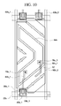
Hereinafter, a liquid crystal panel according to still another embodiment of the present invention will be described in detail with reference to FIG. 10. FIG. 10 is a plan view of a lower display panel included in the liquid crystal panel according to still another exemplary embodiment of the present invention.
Referring to FIG. 10, the liquid crystal panel according to still another exemplary embodiment of the present invention includes first and second subpixel electrodes 82 c_1 and 82 c_2 and a coupling electrode 67.
The first and second subpixel electrodes 82 c_1 and 82 c_2 are spaced apart from each other by a slit 84 b, which is a domain partition portion, and are insulated from each other. In addition, the first and second subpixel electrodes 82 c_1 and 82 c_2 engage with each other to form a pixel region. The first subpixel electrode 82 c_1 is connected to a TFT and receives a data voltage directly from the TFT. A lower data voltage is applied to the second subpixel electrode 82 c_2 than to the first subpixel electrode 82 c_1 by a ‘coupling capacitor’ which is composed of the first subpixel electrode 82 c_1 and the coupling electrode 67.
Each pixel electrode may be cut obliquely at an angle of approximately −45 to +45 degrees with respect to a gate line 22 b and thus partitioned into the first and second subpixel electrodes 82 c_1 and 82 c_2. Therefore, liquid crystals within each pixel may tilt in four directions, thereby securing visibility in the four directions. This arrangement of the first and second subpixel electrodes 82 c_1 and 82 c_2 is a mere exemplary embodiment of the present invention. That is, each pixel electrode may be partitioned in various ways. When necessary, each pixel electrode may be partitioned into three or more subpixel electrodes.
The first and second subpixel electrodes 82 c_1 and 82 c_2 are coupled to each other and operate accordingly. That is, the coupling electrode 67, which is connected to the first subpixel electrode 82 c_1 via contact hole 76 c_3, and the second subpixel electrode 82 c_2 are insulated from each other by a dielectric interposed therebetween and overlap each other to form a ‘coupling capacitor.’ For this reason, if a data voltage is applied to the first subpixel electrode 82 c_1, a voltage lower than the data voltage applied to the first subpixel electrode 82 c_1 is applied to the second subpixel electrode 82 c_2.
The coupling electrode 67 does not have to be connected to the first subpixel electrode 82 c_1. The coupling electrode 67 may alternatively be connected to the second subpixel electrode 82 c_2. That is, if a coupling electrode, which is connected to a second subpixel electrode, and a first subpixel electrode overlap each other and thus form a ‘coupling capacitor,’ when a data voltage is applied to the second subpixel electrode, a lower voltage may be applied to the first subpixel electrode.
The LCD structured as described above includes a liquid crystal layer whose ratio Δ∈/∈⊥ of the dielectric anisotropy Δ∈ to the vertical dielectric constant ∈⊥ may be 0.5 or less and whose rotational viscosity γ1 may be 90 to 110 mPa·S. Thus, the LCD can maintain superior display quality in a stable manner without requiring a storage wiring. In addition, if the driving frequency of the LCD is a high frequency, even though the storage wiring is not formed, the interval at which the data voltage is applied to the first to third subpixel electrodes 82 c_1, 82 c_2 and 82 c_3 becomes small, and a reduction in the magnitude of the data voltage is small. Besides, when the storage wiring is removed, it is possible to increase an aperture ratio of the LCD.
Hereinafter, a liquid crystal panel according to still another exemplary embodiment of the present invention will be described in detail with reference to FIG. 11. FIG. 11 is a plan view of a lower display panel included in the liquid crystal panel according to still another exemplary embodiment of the present invention.
Referring to FIG. 11, a decoupling line 24 b crosses first and second subpixel electrodes 82 b_1 and 82 b_2 and extends substantially parallel to a gate line 22 b. The decoupling line 24 b delivers a decoupling voltage to a first decoupling electrode 25 b_1 and a second decoupling electrode 25 b_2. The decoupling line 24 b may be used to repair defective pixel electrodes. For example, if the first subpixel electrode 82 b_1 is defective, the first subpixel electrode 82 b_1 and the decoupling line 24 b may be made to short-circuit by laser welding. Then, a corresponding pixel may become an ‘off’ pixel.
The decoupling line 24 b may be on the same layer as the gate wiring and may have a width of 5 to 15 μm. Decoupling capacitance may be 5 to 20% of liquid capacitance. That is, the capacitance of a capacitor, which is formed by the overlapping of the decoupling line 24 b with the first subpixel electrode 82 b_1 or the second subpixel electrode 82 b_2, may be reduced to such an extent that the capacitor substantially cannot function as a storage capacitor. The capacitance of the decoupling line 24 b may be sufficient to allow it to function as wiring that applies a voltage to the first and second decoupling electrodes 25 b_1 and 25 b_2. The capacitance of the decoupling line 24 b may be 10% or less of the liquid capacitance.
First and second data lines 62 b_1 and 62 b_2 cross the gate wiring. The first data line 62 b_1 delivers a first data voltage to the first subpixel electrode 82 b_1, and the second data line 62 b_2 delivers a second data voltage to the second subpixel electrode 82 b_2.
The first subpixel electrode 82 b_1 is connected to the gate line 22 b and the first data line 62 b_1 by a switching element to receive a gate signal and the first data voltage. The second subpixel electrode 82 b_2 is connected to the gate line 22 b and the second data line 62 b_2 by a switching element to receive the gate signal and the second data voltage. In this case, the first data voltage may be relatively higher than a common voltage, and the second data voltage may be relatively lower than the common voltage.
A relatively high data voltage is applied to the first subpixel electrode 82 b_1, and a relatively low data voltage is applied to the second subpixel electrode 82 b_2. At a low grayscale level, liquid crystals arranged on the second subpixel electrode 82 b_2, to which a relatively low data voltage is applied, are aligned such that their directors are perpendicular to the lower display panel. Thus, light emitted from a backlight (not shown) cannot pass through the second subpixel electrode 82 b_2.
In this regard, if the second subpixel electrode 82 b_2 overlaps the first and second data lines 62 b_1 and 62 b_2, it blocks light, which is generated around the first and second data lines 62 b_1 and 62 b_2, at a low grayscale level, which may prevent leakage of the light.
The first and second decoupling electrodes 25 b_1 and 25 b_2 are connected to the decoupling line 24 b to receive a decoupling voltage from the decoupling line 24 b. The first and second decoupling electrodes 25 b_1 and 25 b_2 prevent the first subpixel electrode 82 b_1 from being coupled to the first and second data lines 62 b_1 and 62 b_2, respectively. The first and second decoupling electrodes 25 b_1 and 25 b_2 are arranged parallel to the first and second data lines 62 b_1 and 62 b_2 and extend between the first subpixel electrode 82 b_1 and the first and second data lines 62 b_1 and 62 b_2, respectively.
The first and second decoupling electrodes 25 b_1 and 25 b_2 prevent leakage of light between the first and second subpixel electrodes 82 b_1 and 82 b_2 and the first and second data lines 62 b_1 and 62 b_2. When necessary, the first and second decoupling electrodes 25 b_1 and 25 b_2 may partially overlap the first subpixel electrode 82 b_1, the second subpixel electrode 82 b_2, the first data line 62 b_1 or the second data line 62 b_2. The first and second decoupling electrodes 25 b_1 and 25 b_2 may reduce the difference between the coupling capacitance of the first subpixel electrode 82 b_1 and the first data line 62 b_1 and that of the first subpixel electrode 82 b_1 and the second data line 62 b_2.
Hereinafter, a liquid crystal panel according to still another exemplary embodiment of the present invention will be described in detail with reference to FIG. 12. FIG. 12 is a plan view of a lower display panel included in the liquid crystal panel according to still another exemplary embodiment of the present invention. The liquid crystal panel according to still another exemplary embodiment of the present invention includes a decoupling electrode 25 d which overlaps a slit 84 b between first and second subpixel electrodes 82 b_1 and 82 b_2. The first subpixel electrode 82 b_1 is surrounded by the second subpixel electrode 82 b_2 and spaced apart from the second subpixel electrode 82 b_2 by the slit 84 b. The slit 84 b may be at an angle of approximately −45 to +45 degrees with respect to a gate line 22 b. The decoupling electrode 25 d is connected to a decoupling electrode of an adjacent pixel by a decoupling line 24 b.
In order to increase the overall pixel aperture ratio, the decoupling line 25 d may extend parallel to the gate line 22 b and across the center of the second subpixel electrode 82 b_2. In addition, the decoupling line 25 d may not overlap the first subpixel electrode 82 b_1. That is, the decoupling line 25 d may be shaped like a hollow trapezoid or English character ‘V’, which lies laterally and has an empty space therein, and may be disposed parallel to the first subpixel electrode 82 b_1.
It will be apparent to those skilled in the art that various modifications and variations can be made in the present invention without departing from the spirit or scope of the invention. Thus, it is intended that the present invention cover the modifications and variations of this invention provided they come within the scope of the appended claims and their equivalents.

Claims (9)

What is claimed is:
1. A liquid crystal display (LCD) comprising:
a liquid crystal panel; and
a gate driver configured to apply a gate signal having a driving frequency equal to or greater than 100 Hz to the liquid crystal panel,
wherein:
the liquid crystal panel comprises:
a first display panel;
a second display panel facing the first display panel;
a liquid crystal composition disposed between the first display panel and the second display panel and includes liquid crystals;
a first gate line and a second gate line disposed on the first display panel;
a data line that crosses the first gate line and the second gate line;
a control line extending parallel to the first and second gate lines and disposed between the first and second gate lines;
a first subpixel electrode disposed on the first display panel and connected to the first gate line by a first switching element;
a second subpixel electrode disposed on the first display panel, spaced apart from the first subpixel electrode, and connected to the first gate line by a second switching element;
a control switching element that is switched on or off in response to a gate signal transmitted from the second gate line and is connected to the second subpixel electrode;
a first control electrode that is connected to the control switching element, the first control electrode being disposed in the same layer as the first and second subpixel electrodes, the first control electrode being separated from the first and second subpixel electrodes; and
a second control electrode which overlaps the first control electrode to form a control capacitor configured to receive a control voltage, the second control electrode branching off from the control line and being disposed in the same layer as the first and second gate lines;
if a dielectric constant in a direction parallel to a long axis of liquid crystals is defined as a horizontal dielectric constant ∈∥, a dielectric constant in a direction perpendicular to the long axis of the liquid crystals is defined as a vertical dielectric constant ∈⊥, and the difference between the vertical dielectric constant ∈⊥ and the horizontal dielectric constant ∈∥ is defined as dielectric anisotropy Δ∈, then a ratio Δ∈/∈⊥ of the dielectric anisotropy Δ∈ to the vertical dielectric constant ∈⊥ of the liquid crystal composition is 0.5 or less; and
the first subpixel electrode and the second subpixel electrode are bent in a zigzag manner.
2. The LCD of claim 1, wherein the driving frequency is a multiple of 60 Hz.
3. The LCD of claim 1, wherein a rotational viscosity of the liquid crystal composition is 90 to 100 mPa·S.
4. The LCD of claim 1, wherein the liquid crystal composition includes 10 to 30 weight % of an alkenyl.
5. The LCD of claim 1, wherein the first control electrode is made of indium tin oxide (ITO) or indium zinc oxide (IZO).
6. The LCD of claim 1, wherein the control voltage is a common voltage.
7. The LCD of claim 1, wherein the liquid crystal panel further comprises a black matrix disposed on the first display panel or the second display panel and overlapping the first control electrode and the second control electrode.
8. The LCD of claim 1, wherein the second gate line is a gate line of an adjacent pixel.
9. The LCD of claim 1, further comprising a slit arranged between the first subpixel electrode and the second subpixel electrode, the slit being at an angle of −45 to +45 degrees with respect to the gate line.
US13/599,414 2008-01-21 2012-08-30 Liquid crystal display Expired - Fee Related US9341896B2 (en)

Priority Applications (1)

Application Number Priority Date Filing Date Title
US13/599,414 US9341896B2 (en) 2008-01-21 2012-08-30 Liquid crystal display

Applications Claiming Priority (4)

Application Number Priority Date Filing Date Title
KR10-2008-0006346 2008-01-21
KR1020080006346A KR101443856B1 (en) 2008-01-21 2008-01-21 Liquid crystal display device and liquid crystal composition included therein
US12/356,370 US8610867B2 (en) 2008-01-21 2009-01-20 Liquid crystal display and liquid crystal composition included therein
US13/599,414 US9341896B2 (en) 2008-01-21 2012-08-30 Liquid crystal display

Related Parent Applications (1)

Application Number Title Priority Date Filing Date
US12/356,370 Continuation-In-Part US8610867B2 (en) 2008-01-21 2009-01-20 Liquid crystal display and liquid crystal composition included therein

Publications (2)

Publication Number Publication Date
US20120320294A1 US20120320294A1 (en) 2012-12-20
US9341896B2 true US9341896B2 (en) 2016-05-17

Family

ID=47353414

Family Applications (1)

Application Number Title Priority Date Filing Date
US13/599,414 Expired - Fee Related US9341896B2 (en) 2008-01-21 2012-08-30 Liquid crystal display

Country Status (1)

Country Link
US (1) US9341896B2 (en)

Families Citing this family (4)

* Cited by examiner, † Cited by third party
Publication number Priority date Publication date Assignee Title
WO2013038454A1 (en) * 2011-09-15 2013-03-21 パナソニック株式会社 Organic el element manufacturing method and evaluation method
KR20140088810A (en) * 2013-01-03 2014-07-11 삼성디스플레이 주식회사 Thin film transistor panel and method for manufacturing the same
KR102160112B1 (en) * 2014-03-06 2020-09-28 삼성디스플레이 주식회사 Liquid crystal display
CN108957888B (en) * 2018-07-27 2021-07-16 厦门天马微电子有限公司 Display panel and display device

Citations (17)

* Cited by examiner, † Cited by third party
Publication number Priority date Publication date Assignee Title
EP1054321A2 (en) 1999-05-21 2000-11-22 Sony Corporation Information processing method and apparatus
US20010045545A1 (en) 1998-09-12 2001-11-29 Kazuaki Tarumi Liquid-crystalline medium, and liquid-crystal display containing same
KR20030025685A (en) 2001-09-22 2003-03-29 삼성전자주식회사 Liquid crystal display device
US20030136944A1 (en) 1998-04-22 2003-07-24 Dainippon Ink And Chemicals, Inc. Naphthalene derivative and liquid crystal composition comprising the same
CN1637513A (en) 2004-12-08 2005-07-13 河北工业大学 Coplanar converting LCD with video response
JP2005338818A (en) 2004-05-13 2005-12-08 Quanta Display Inc Liquid crystal display device having no storage capacitor electrode line
CN1723260A (en) 2002-12-11 2006-01-18 默克专利股份有限公司 Fast Switching Liquid Crystal Compositions for Bistable Liquid Crystal Devices
US6992742B2 (en) 1999-03-09 2006-01-31 Lg.Philips Lcd Co., Ltd. Multi-domain liquid crystal display device having pixel electrodes with electric field inducing windows
JP2006048055A (en) 2004-08-04 2006-02-16 Samsung Electronics Co Ltd Thin film transistor display panel and liquid crystal display device including the display panel
US20060103800A1 (en) 2004-10-29 2006-05-18 Wang-Yang Li Multi-domain vertically aligned liquid crystal display
KR20060083633A (en) 2005-01-18 2006-07-21 삼성전자주식회사 LCD Display
US20060221277A1 (en) 2005-03-30 2006-10-05 Samsung Electronics Co., Ltd. Transreflective liquid crystal display
KR20070006981A (en) 2005-07-09 2007-01-12 삼성전자주식회사 Liquid crystal display
US20070146283A1 (en) * 2005-12-27 2007-06-28 Lg Philips Lcd Co., Ltd. Liquid crystal display and driving method thereof
EP1872948A2 (en) 2006-06-28 2008-01-02 Canon Kabushiki Kaisha Printhead, head cartridge, and printing apparatus employing either of same
US20080143912A1 (en) * 2006-12-18 2008-06-19 Dong-Gyu Kim Thin film transistor substrate and method of manufacturing the same
US20110102695A1 (en) 2007-09-07 2011-05-05 Takashi Katayama Liquid crystal display device driving method and liquid crystal display device

Patent Citations (21)

* Cited by examiner, † Cited by third party
Publication number Priority date Publication date Assignee Title
US20030136944A1 (en) 1998-04-22 2003-07-24 Dainippon Ink And Chemicals, Inc. Naphthalene derivative and liquid crystal composition comprising the same
US20010045545A1 (en) 1998-09-12 2001-11-29 Kazuaki Tarumi Liquid-crystalline medium, and liquid-crystal display containing same
US6992742B2 (en) 1999-03-09 2006-01-31 Lg.Philips Lcd Co., Ltd. Multi-domain liquid crystal display device having pixel electrodes with electric field inducing windows
CN1282039A (en) 1999-05-21 2001-01-31 索尼株式会社 Information processing method and device
EP1054321A2 (en) 1999-05-21 2000-11-22 Sony Corporation Information processing method and apparatus
KR20030025685A (en) 2001-09-22 2003-03-29 삼성전자주식회사 Liquid crystal display device
CN1723260A (en) 2002-12-11 2006-01-18 默克专利股份有限公司 Fast Switching Liquid Crystal Compositions for Bistable Liquid Crystal Devices
JP2005338818A (en) 2004-05-13 2005-12-08 Quanta Display Inc Liquid crystal display device having no storage capacitor electrode line
US7499129B2 (en) 2004-08-04 2009-03-03 Samsung Electronics Co., Ltd. Thin film transistor array panel and LCD having plural red, green and blue pixels in which each color pixel includes first and second subpixel electrodes having different voltage/area ratios with respect to each other and for each color pixel
JP2006048055A (en) 2004-08-04 2006-02-16 Samsung Electronics Co Ltd Thin film transistor display panel and liquid crystal display device including the display panel
US20060103800A1 (en) 2004-10-29 2006-05-18 Wang-Yang Li Multi-domain vertically aligned liquid crystal display
CN1637513A (en) 2004-12-08 2005-07-13 河北工业大学 Coplanar converting LCD with video response
KR20060083633A (en) 2005-01-18 2006-07-21 삼성전자주식회사 LCD Display
US7768582B2 (en) 2005-01-18 2010-08-03 Samsung Electronics Co., Ltd. Liquid crystal display
US20060221277A1 (en) 2005-03-30 2006-10-05 Samsung Electronics Co., Ltd. Transreflective liquid crystal display
KR20070006981A (en) 2005-07-09 2007-01-12 삼성전자주식회사 Liquid crystal display
US20070146283A1 (en) * 2005-12-27 2007-06-28 Lg Philips Lcd Co., Ltd. Liquid crystal display and driving method thereof
EP1872948A2 (en) 2006-06-28 2008-01-02 Canon Kabushiki Kaisha Printhead, head cartridge, and printing apparatus employing either of same
CN101096140A (en) 2006-06-28 2008-01-02 佳能株式会社 Printhead, head cartridge, and printing apparatus employing either of same
US20080143912A1 (en) * 2006-12-18 2008-06-19 Dong-Gyu Kim Thin film transistor substrate and method of manufacturing the same
US20110102695A1 (en) 2007-09-07 2011-05-05 Takashi Katayama Liquid crystal display device driving method and liquid crystal display device

Non-Patent Citations (7)

* Cited by examiner, † Cited by third party
Title
Chinese Office Action dated Jun. 18, 2012 issued for Chinese Patent Application No. 200910005055.0.
Chinese Office Action dated Sep. 27, 2011 issued for Chinese Patent Application No. 200910005055.0.
Corrected Notice of Allowance and Fee(s) Due dated Sep. 6, 2013 in U.S. Appl. No. 12/356,370.
Final Office Action dated May 3, 2012 issued for co-pending U.S. Appl. No. 12/356,370.
Final Office Action issued on May 21, 2013 in U.S. Appl. No. 12/356,370.
Non-Final Office Action dated Dec. 5, 2011 issued for co-pending U.S. Appl. No. 12/356,370.
Non-Final Office Action issued on Dec. 17, 2012 in U.S. Appl. No. 12/356,370.

Also Published As

Publication number Publication date
US20120320294A1 (en) 2012-12-20

Similar Documents

Publication Publication Date Title
US7746438B2 (en) Liquid crystal display device and method of driving thereof
US8610867B2 (en) Liquid crystal display and liquid crystal composition included therein
US7618689B2 (en) Liquid crystal composition and liquid crystal display having the same
US8553192B2 (en) Liquid crystal display
CN101546079A (en) Liquid crystal display, thin film transistor substrate and method for improving the display quality
US8497968B2 (en) Liquid crystal display having capacitance-coupled floating electrode
KR101074396B1 (en) In-plane switching mode liquid crystal display device
US7760282B2 (en) Liquid crystal display
US10324321B2 (en) Display device
US7929099B2 (en) Liquid crystal display with improved lateral visibility
US9341896B2 (en) Liquid crystal display
KR20100047575A (en) Liquid crystal display
US20160282691A1 (en) Liquid crystal display device
KR20060114921A (en) Liquid crystal display
US8253912B2 (en) Liquid crystal display
US20070002260A1 (en) Liquid crystal display
KR20080047788A (en) Liquid crystal display
KR20080098882A (en) Liquid crystal display
JP2007004171A (en) Liquid crystal display
JP2009047963A (en) Liquid crystal device and electronic device
KR20070121112A (en) Liquid crystal display

Legal Events

Date Code Title Description
AS Assignment

Owner name: SAMSUNG DISPLAY CO., LTD., KOREA, REPUBLIC OF

Free format text: ASSIGNMENT OF ASSIGNORS INTEREST;ASSIGNORS:KIM, DONG-GYU;SHIN, KYOUNG-JU;SON, JONG-HO;AND OTHERS;REEL/FRAME:028877/0227

Effective date: 20120828

FEPP Fee payment procedure

Free format text: PAYOR NUMBER ASSIGNED (ORIGINAL EVENT CODE: ASPN); ENTITY STATUS OF PATENT OWNER: LARGE ENTITY

STCF Information on status: patent grant

Free format text: PATENTED CASE

FEPP Fee payment procedure

Free format text: MAINTENANCE FEE REMINDER MAILED (ORIGINAL EVENT CODE: REM.); ENTITY STATUS OF PATENT OWNER: LARGE ENTITY

LAPS Lapse for failure to pay maintenance fees

Free format text: PATENT EXPIRED FOR FAILURE TO PAY MAINTENANCE FEES (ORIGINAL EVENT CODE: EXP.); ENTITY STATUS OF PATENT OWNER: LARGE ENTITY

STCH Information on status: patent discontinuation

Free format text: PATENT EXPIRED DUE TO NONPAYMENT OF MAINTENANCE FEES UNDER 37 CFR 1.362

FP Lapsed due to failure to pay maintenance fee

Effective date: 20200517