US9335494B2 - Optoelectronics structures - Google Patents
Optoelectronics structures Download PDFInfo
- Publication number
- US9335494B2 US9335494B2 US14/278,588 US201414278588A US9335494B2 US 9335494 B2 US9335494 B2 US 9335494B2 US 201414278588 A US201414278588 A US 201414278588A US 9335494 B2 US9335494 B2 US 9335494B2
- Authority
- US
- United States
- Prior art keywords
- substrate
- optoelectronics
- vcsel
- optical fiber
- fiber
- Prior art date
- Legal status (The legal status is an assumption and is not a legal conclusion. Google has not performed a legal analysis and makes no representation as to the accuracy of the status listed.)
- Expired - Fee Related
Links
- 230000005693 optoelectronics Effects 0.000 title claims abstract description 38
- 239000000758 substrate Substances 0.000 claims abstract description 75
- 239000000835 fiber Substances 0.000 claims abstract description 38
- 239000013307 optical fiber Substances 0.000 claims abstract description 34
- 239000011521 glass Substances 0.000 claims description 23
- 230000008878 coupling Effects 0.000 description 20
- 238000010168 coupling process Methods 0.000 description 20
- 238000005859 coupling reaction Methods 0.000 description 20
- 230000003287 optical effect Effects 0.000 description 16
- 229910052710 silicon Inorganic materials 0.000 description 10
- 239000010703 silicon Substances 0.000 description 10
- XUIMIQQOPSSXEZ-UHFFFAOYSA-N Silicon Chemical compound [Si] XUIMIQQOPSSXEZ-UHFFFAOYSA-N 0.000 description 9
- 239000000463 material Substances 0.000 description 9
- 239000000853 adhesive Substances 0.000 description 6
- 230000001070 adhesive effect Effects 0.000 description 6
- 229910000679 solder Inorganic materials 0.000 description 6
- 238000005530 etching Methods 0.000 description 5
- 238000000034 method Methods 0.000 description 5
- RYGMFSIKBFXOCR-UHFFFAOYSA-N Copper Chemical compound [Cu] RYGMFSIKBFXOCR-UHFFFAOYSA-N 0.000 description 3
- 229910052802 copper Inorganic materials 0.000 description 3
- 239000010949 copper Substances 0.000 description 3
- 238000013461 design Methods 0.000 description 3
- 238000003780 insertion Methods 0.000 description 3
- 230000037431 insertion Effects 0.000 description 3
- 239000004065 semiconductor Substances 0.000 description 3
- 239000002313 adhesive film Substances 0.000 description 2
- 238000000708 deep reactive-ion etching Methods 0.000 description 2
- PCHJSUWPFVWCPO-UHFFFAOYSA-N gold Chemical compound [Au] PCHJSUWPFVWCPO-UHFFFAOYSA-N 0.000 description 2
- 229910052737 gold Inorganic materials 0.000 description 2
- 239000010931 gold Substances 0.000 description 2
- 238000010329 laser etching Methods 0.000 description 2
- 238000004519 manufacturing process Methods 0.000 description 2
- 229910052751 metal Inorganic materials 0.000 description 2
- 239000002184 metal Substances 0.000 description 2
- -1 optical underfills Substances 0.000 description 2
- 238000004806 packaging method and process Methods 0.000 description 2
- 238000004088 simulation Methods 0.000 description 2
- 239000000126 substance Substances 0.000 description 2
- BQCADISMDOOEFD-UHFFFAOYSA-N Silver Chemical compound [Ag] BQCADISMDOOEFD-UHFFFAOYSA-N 0.000 description 1
- 229910045601 alloy Inorganic materials 0.000 description 1
- 239000000956 alloy Substances 0.000 description 1
- 229910052782 aluminium Inorganic materials 0.000 description 1
- XAGFODPZIPBFFR-UHFFFAOYSA-N aluminium Chemical compound [Al] XAGFODPZIPBFFR-UHFFFAOYSA-N 0.000 description 1
- 238000003491 array Methods 0.000 description 1
- 238000004891 communication Methods 0.000 description 1
- 239000004020 conductor Substances 0.000 description 1
- 230000007547 defect Effects 0.000 description 1
- 239000003822 epoxy resin Substances 0.000 description 1
- LNEPOXFFQSENCJ-UHFFFAOYSA-N haloperidol Chemical compound C1CC(O)(C=2C=CC(Cl)=CC=2)CCN1CCCC(=O)C1=CC=C(F)C=C1 LNEPOXFFQSENCJ-UHFFFAOYSA-N 0.000 description 1
- 238000007641 inkjet printing Methods 0.000 description 1
- 239000012212 insulator Substances 0.000 description 1
- 238000002955 isolation Methods 0.000 description 1
- 238000001459 lithography Methods 0.000 description 1
- 238000012986 modification Methods 0.000 description 1
- 230000004048 modification Effects 0.000 description 1
- 238000013041 optical simulation Methods 0.000 description 1
- 238000000206 photolithography Methods 0.000 description 1
- 229920002120 photoresistant polymer Polymers 0.000 description 1
- 238000007747 plating Methods 0.000 description 1
- 150000003071 polychlorinated biphenyls Chemical group 0.000 description 1
- 229920000647 polyepoxide Polymers 0.000 description 1
- 229920000642 polymer Polymers 0.000 description 1
- 229910052709 silver Inorganic materials 0.000 description 1
- 239000004332 silver Substances 0.000 description 1
Images


Classifications
-
- G—PHYSICS
- G02—OPTICS
- G02B—OPTICAL ELEMENTS, SYSTEMS OR APPARATUS
- G02B6/00—Light guides; Structural details of arrangements comprising light guides and other optical elements, e.g. couplings
- G02B6/24—Coupling light guides
- G02B6/42—Coupling light guides with opto-electronic elements
- G02B6/4201—Packages, e.g. shape, construction, internal or external details
- G02B6/4204—Packages, e.g. shape, construction, internal or external details the coupling comprising intermediate optical elements, e.g. lenses, holograms
- G02B6/4206—Optical features
-
- G—PHYSICS
- G02—OPTICS
- G02B—OPTICAL ELEMENTS, SYSTEMS OR APPARATUS
- G02B6/00—Light guides; Structural details of arrangements comprising light guides and other optical elements, e.g. couplings
- G02B6/24—Coupling light guides
- G02B6/42—Coupling light guides with opto-electronic elements
- G02B6/4201—Packages, e.g. shape, construction, internal or external details
- G02B6/4219—Mechanical fixtures for holding or positioning the elements relative to each other in the couplings; Alignment methods for the elements, e.g. measuring or observing methods especially used therefor
- G02B6/422—Active alignment, i.e. moving the elements in response to the detected degree of coupling or position of the elements
-
- G—PHYSICS
- G02—OPTICS
- G02B—OPTICAL ELEMENTS, SYSTEMS OR APPARATUS
- G02B6/00—Light guides; Structural details of arrangements comprising light guides and other optical elements, e.g. couplings
- G02B6/24—Coupling light guides
- G02B6/42—Coupling light guides with opto-electronic elements
- G02B6/4201—Packages, e.g. shape, construction, internal or external details
- G02B6/4219—Mechanical fixtures for holding or positioning the elements relative to each other in the couplings; Alignment methods for the elements, e.g. measuring or observing methods especially used therefor
- G02B6/4228—Passive alignment, i.e. without a detection of the degree of coupling or the position of the elements
- G02B6/423—Passive alignment, i.e. without a detection of the degree of coupling or the position of the elements using guiding surfaces for the alignment
-
- G—PHYSICS
- G02—OPTICS
- G02B—OPTICAL ELEMENTS, SYSTEMS OR APPARATUS
- G02B6/00—Light guides; Structural details of arrangements comprising light guides and other optical elements, e.g. couplings
- G02B6/24—Coupling light guides
- G02B6/42—Coupling light guides with opto-electronic elements
- G02B6/4201—Packages, e.g. shape, construction, internal or external details
- G02B6/4249—Packages, e.g. shape, construction, internal or external details comprising arrays of active devices and fibres
- G02B6/425—Optical features
-
- G—PHYSICS
- G02—OPTICS
- G02B—OPTICAL ELEMENTS, SYSTEMS OR APPARATUS
- G02B6/00—Light guides; Structural details of arrangements comprising light guides and other optical elements, e.g. couplings
- G02B6/24—Coupling light guides
- G02B6/36—Mechanical coupling means
- G02B6/3628—Mechanical coupling means for mounting fibres to supporting carriers
- G02B6/3648—Supporting carriers of a microbench type, i.e. with micromachined additional mechanical structures
- G02B6/3652—Supporting carriers of a microbench type, i.e. with micromachined additional mechanical structures the additional structures being prepositioning mounting areas, allowing only movement in one dimension, e.g. grooves, trenches or vias in the microbench surface, i.e. self aligning supporting carriers
-
- G—PHYSICS
- G02—OPTICS
- G02B—OPTICAL ELEMENTS, SYSTEMS OR APPARATUS
- G02B6/00—Light guides; Structural details of arrangements comprising light guides and other optical elements, e.g. couplings
- G02B6/24—Coupling light guides
- G02B6/42—Coupling light guides with opto-electronic elements
- G02B6/4201—Packages, e.g. shape, construction, internal or external details
- G02B6/4202—Packages, e.g. shape, construction, internal or external details for coupling an active element with fibres without intermediate optical elements, e.g. fibres with plane ends, fibres with shaped ends, bundles
-
- G—PHYSICS
- G02—OPTICS
- G02B—OPTICAL ELEMENTS, SYSTEMS OR APPARATUS
- G02B6/00—Light guides; Structural details of arrangements comprising light guides and other optical elements, e.g. couplings
- G02B6/24—Coupling light guides
- G02B6/42—Coupling light guides with opto-electronic elements
- G02B6/4201—Packages, e.g. shape, construction, internal or external details
- G02B6/4219—Mechanical fixtures for holding or positioning the elements relative to each other in the couplings; Alignment methods for the elements, e.g. measuring or observing methods especially used therefor
- G02B6/4236—Fixing or mounting methods of the aligned elements
- G02B6/424—Mounting of the optical light guide
- G02B6/4243—Mounting of the optical light guide into a groove
-
- G—PHYSICS
- G02—OPTICS
- G02B—OPTICAL ELEMENTS, SYSTEMS OR APPARATUS
- G02B6/00—Light guides; Structural details of arrangements comprising light guides and other optical elements, e.g. couplings
- G02B6/24—Coupling light guides
- G02B6/42—Coupling light guides with opto-electronic elements
- G02B6/4201—Packages, e.g. shape, construction, internal or external details
- G02B6/4219—Mechanical fixtures for holding or positioning the elements relative to each other in the couplings; Alignment methods for the elements, e.g. measuring or observing methods especially used therefor
- G02B6/4236—Fixing or mounting methods of the aligned elements
- G02B6/4245—Mounting of the opto-electronic elements
Definitions
- VCSEL vertical-cavity surface-emitting laser
- transceivers involves complicated 3-dimensional assembly of VCSELs, integrated circuits (ICs), photodetector chips, and the like including alignment and coupling with stacks of optical elements such as lens arrays, turning mirrors, and fiber ferrules.
- the current packaging scheme also involves several materials such as optical underfills, adhesives, and thermal interface materials, each of which is poses potential interfacial defects.
- the current assembly is mostly manual, and thus is time consuming with low throughput.
- One aspect of the invention provides an optoelectronics structure including: a substrate defining a trench on a first surface; and a VCSEL structure mounted vertically within the trench of the substrate such that the VCSEL structure emits a laser beam substantially parallel to the substrate.
- the substrate can include glass or silicon.
- the optoelectronics structure can further include an optical fiber mounted on the substrate substantially coaxial with the laser beam emitted by the VCSEL structure.
- the optoelectronics structure can further include a fiber guide positioned between the optical fiber and the substrate.
- the optoelectronics structure can further include a lens mounted between and substantially coaxial with a laser-emitting surface of the VCSEL structure and the optical fiber.
- the optoelectronics structure can further include a waveguide or lens mounted on a laser-emitting surface of the VCSEL structure.
- the optoelectronics structure can further include an electrical connection from the VCSEL structure to a second, opposite surface of the substrate.
- an optoelectronics structure including: an fiber guiding substrate defining a trench on a first surface; a VCSEL structure mounted vertically within the trench of the fiber guiding substrate such that the VCSEL structure emits a laser beam substantially parallel to the substrate; and an optical fiber mounted on the fiber guiding substrate substantially coaxial with the laser beam emitted by the VCSEL structure.
- an optoelectronics structure including: a substrate defining a trench on a first surface; and a PIN diode structure mounted vertically within the trench of the substrate such that the PIN diode structure receives a light beam substantially parallel to the substrate.
- the substrate can include glass or silicon.
- the optoelectronics structure can further include an optical fiber mounted on the substrate substantially coaxial with the PIN diode structure.
- the optoelectronics structure can further include a fiber guide positioned between the optical fiber and the substrate.
- the optoelectronics structure can further include a lens mounted between and substantially coaxial with the PIN diode structure and the optical fiber.
- the optoelectronics structure can further include a waveguide or lens mounted on the optical fiber.
- the optoelectronics structure can further include an electrical connection from the PIN diode structure to a second, opposite surface of the substrate.
- FIG. 1 depicts an optoelectronics structures according to embodiments of the invention
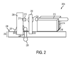
- FIG. 2 depicts an optoelectronics structures according to embodiments of the invention
- FIGS. 3A-3C depict optoelectronics structures according to embodiments of the invention.
- FIGS. 4A and 4B depict the simulated optical coupling performance of a microlens mounted on a glass substrate with a VCSEL structure
- FIGS. 5A and 5B depict the simulated optical coupling performance of a discrete lens array structure aligned with a VCSEL structure
- FIGS. 6A and 6B depict the simulated optical coupling performance of direct coupling of an optical fiber with a VCSEL structure
- FIGS. 7A and 7B depict the simulated optical coupling performance of a multimode fiber and a PIN diode.
- FIGS. 8A and 8B depict the simulated optical coupling performance of a lens array on a glass substrate directly bonded on a PIN diode.
- aspects of the invention provide optoelectronics structures including a substrate defining a trench on a first surface and a VCSEL structure mounted vertically within the trench of the substrate such that the VCSEL emits a laser beam substantially parallel to the substrate.
- FIG. 1 An exemplary embodiment of such an optoelectronics structure 200 a is depicted in FIG. 1 .
- Substrate 202 can be an insulator such as a glass or silicon interposer. In one embodiment, substrate 202 has a thickness between about 200 ⁇ m and about 225 ⁇ m. Substrate 202 includes a trench 204 on a first surface 206 . Trench 204 can be pre-etched and can have a suitable depth to securely hold a VCSEL structure 208 at a right angle with respect to substrate 202 . VCSEL structure 208 can be held in place by mechanical gripping, an interference fit, solder connections, and/or by chemical bonding facilitated by an adhesive 207 .
- a silicon or glass substrate 202 enables use of standard semiconductor fabrication techniques such as lithography, etching, copper plating, and the like for creating various surface features (such as trenches 204 for VCSEL placement) that enable proper passive alignment.
- Adhesive 207 can be applied within trench 204 prior to insertion of VCSEL structure 208 and/or can be applied to the back side of VCSEL structure 208 as depicted in FIGS. 1 and 2 .
- Adhesive 207 can include any material capable of forming a bond with substrate 202 and VCSEL structure 208 and withstanding reflow temperatures. Suitable adhesives include epoxy resins and the like. Adhesives 207 can be cured (e.g., through the application of thermal or UV energy) in accordance manufacturer instructions.
- VCSEL structure 208 can be any conventional semiconductor laser diode with laser beam emission perpendicular from a top or bottom surface (as opposed to edge-emitting or in-plane semiconductor lasers).
- a VCSEL cavity 210 is formed on a top or bottom surface of the VCSEL structure 208 .
- An optical fiber 212 can be mounted on the substrate 202 to receive a laser beam emitted by the VCSEL structure.
- Optical fiber 212 can be any known optical fiber, for example, those used in fiber optic communication systems.
- Optical fiber 212 can have varying diameters such as about 125 ⁇ m.
- Optical fiber 212 can be coupled to the substrate 202 , for example, by a fiber gripper 214 .
- Fiber gripper 214 can be a block (e.g., a silicon block) with etched grooves (e.g., u-shaped or v-shaped grooves) adapted and configured for fiber placement.
- Fiber gripper 214 can have a sufficient thickness to hold optical fiber 212 in alignment with VCSEL cavity 210 .
- the total thickness of the fiber gripper 214 can be about 259 ⁇ m.
- Fiber gripper 214 can be coupled to substrate 202 with a mechanical fastener (e.g., screws, rivets, and the like) or with a chemical fastener such as an adhesive film 216 (e.g., an adhesive film having a thickness of about 20 ⁇ m).
- a mechanical fastener e.g., screws, rivets, and the like
- a chemical fastener such as an adhesive film 216 (e.g., an adhesive film having a thickness of about 20 ⁇ m).
- the fiber gripper 214 can also be made of photoresist material such as SU-8 and can be directly deposited on substrate 202 via standard wafer or panel level photolithography techniques.
- a waveguide and/or lens 218 can be placed between VCSEL cavity 210 and optical fiber 212 in order to carry, direct, and/or shape the laser beam produced by VCSEL structure 208 .
- Waveguide and/or lens 218 can be formed from a variety of materials such as SU-8. For example, in FIG. 1 , a polymer-based pillar is deposited on the VCSEL cavity and a micro-fabricated lens material is deposited on top of the pillar to focus light on to the optical fiber 212 .
- VCSEL structure 208 can be powered and controlled via one or more bond pads 220 , which can be coupled (e.g., through solder 222 ) to a via 224 that can, in turn, be coupled to another component such as a PCB, e.g., through flip chip or wire bonding. Additionally or alternately, the substrate 202 can have plated metal fan-out circuitry 336 that allows it to be wire-bonded to a PCB board (as can be seen in FIG. 3A ).
- Vias 224 can be formed from a conductive material such as a metal (e.g., copper, aluminum, silver, gold, and alloys thereof) and can terminate on either or both sides of substrate 202 in conductive pads (e.g., having a copper or gold surface finish) and can be positioned along the substrate proximate to bond pads 220 of VCSEL structure 208 .
- Solder paste or flux-and-solder balls 222 can be placed on the substrate 202 with the solder ball height determined based on the height of the VCSEL bond pads 220 . As seen in FIG. 1 , a solder ball 222 between about 100 ⁇ m and about 200 ⁇ m will be sufficient to initiate good contact with the VCSEL bond pad 220 .
- a further glass substrate 230 can be mounted vertically in substrate 202 between VCSEL structure 208 and optical fiber 212 .
- Glass substrate 230 can be mounted in a trench 232 at a substantially right angle with respect to surface 206 of substrate 202 in the same or similar manner to VCSEL structure 208 .
- Glass substrate 230 can include one or more lenses 234 , which can be subwavelength grating (SWG) lenses applied to glass substrate 230 using a variety of techniques such as inkjet printing or thermal reflow.
- SWG subwavelength grating
- the optical fiber 212 can be directly butt coupled to the VCSEL cavity 210 , with a waveguide deposited on top of the VCSEL cavity 210 and the distance between the VCSEL cavity 210 and the optical fiber 212 optimized to take into account any divergence of light from the VCSEL waveguide.
- assembly 300 can also include fan-out pads 336 for wirebonding substrate 302 to a PCB and/or a driver/transimpedance amplifier (TIA) 338 .
- Driver/TIA 338 can optionally be assembled separately with a discrete thermal sink and/or thermal solution.
- driver/TIA 338 could be mounted on the bottom side of silicon/glass interposer 302 and electrically connected to the VCSEL or photodiode chips using electrical vias 324 .
- Mounting driver/TIA 338 chips on the opposite side of substrate 302 advantageously thermally isolates components of assembly.
- bumps 320 can act as mechanical stops to facilitate the z-height alignment of the VCSEL structure 308 .
- Optimal alignment and coupling efficiency can be achieved by controlling one or more parameters during design and manufacturing.
- trench depth for the VCSEL structure 208 , 308 and lens array can be accurate to within a micron.
- Suitable etching techniques for achieving such precise depths include photolithographic etching of glass/silicon, deep reactive ion etching, and laser etching.
- Fiber gripper thickness and trench depth can also be optimized to control the positioning of optical fibers 212 , 312 .
- Suitable etching techniques for achieving such precise depths include photolithographic etching of glass/silicon, deep reactive ion etching, and laser etching.
- Die attach films are available in 20-30 ⁇ m thicknesses and have good uniformity (tolerances between 0.5-1 ⁇ m) and can be utilized to mount fiber gripper to substrate 202 , 302 .
- Alignment between the VCSEL cavity, the lens array (deposited or discrete), and the optical fiber array in the z-direction can also be improved by design and control of the efficiency of the lens material (including loss from any waveguide material) and any tilts in VCSEL placement or fiber placement.
- FIGS. 4A and 5B optical simulations were performed using various coupling arrangements. Simulations were performed using software from Zemax, LLC of Redmond, Wash. The simulation results depict some exemplary dimensions of the lens structures and relative distances of the VCSEL from the lens and the fiber array and can be used to design transceiver packages to achieve maximum efficiencies.
- Microlens 418 a has a thickness h l varying from 20 to 45 ⁇ m.
- Fiber placement distance t lf varied from 0.2 to 1.1 mm.
- lens thickness of 25 ⁇ m and 30 ⁇ m provided the best results (87% coupling, 0.6 dB loss) for VCSEL to fiber coupling.
- FIG. 5A a discrete lens array structure is aligned to the VCSEL cavity as described and depicted in the context of FIG. 2 .
- FIG. 5B depicts the coupling efficiency on the y-axis as a function of fiber distance from the discrete lens structure in order to achieve maximum coupling efficiency.
- FIG. 6A simulates the direct coupling of a VCSEL to an optical fiber 612 .
- 850 nm light is launched from the VCSEL and is directly collected by a 50/125 multimode fiber 612 .
- the VCSEL has an aperture diameter of 14 ⁇ m, a beam divergence half angle of 16° (from virtual point source 646 ), a fiber placement distance t lf (from VCSEL emitting facet 648 ) varying from 0 to 0.5 mm.
- FIG. 6B around 70% of the total optical power (1.5 dB loss) from the VCSEL can be coupled into the fiber. Additionally, the use of an optical underfill can enable slightly better coupling efficiency.
- the principles described herein in the context of VCSEL packages 208 , 308 can also be applied to PIN diodes, for example, for use as photosensors.
- PIN diodes would replace VCSEL structures 208 , 308 and would receive light via optical fiber 212 and produce a current.
- FIG. 7A Such an embodiment is simulated in FIG. 7A .
- Light is launched from a 50/125 multimode fiber and directly collected by a PIN diode 754 .
- Optical underfill can slightly improve coupling efficiency.
- FIG. 8A Another embodiment is simulated in FIG. 8A .
- microlenses 818 a having a varying thickness h l of 30 ⁇ m and thicker produced the best results, collecting 95% light with 0.2 dB loss.
- aspects and embodiments of the invention described herein have a number of advantages over conventional structures. Generally speaking, aspects of the invention provide highly scalable packaging with reduced material and assembly costs. Additionally, aspects of the invention facilitate automated assembly for higher yield and throughput.
- glass substrates 202 , 302 are particularly advantageous because glass substrates 202 , 302 are widely available in thin panel form without chemical-mechanical planarization and at a low cost (typically between about 0.003 to about 0.005 USD). Glass also has a low dielectric constant and low insertion low, allowing for denser high-speed signal connection. Glass substrates also provide thermal isolation of components for better thermal management. Glass substrates also have similar rigidity and coefficients of thermal expansion as silicon PCBs, resulting in low warpage and low stress packages.
- embodiments of the invention that place a lens directly on the VCSEL structure and/or directly couple optical fibers to the VCSEL structure reduce tolerance stack-ups and optical coupling variations and produce low loss, more efficient optical coupling than traditional VCSEL-based packages.
Landscapes
- Physics & Mathematics (AREA)
- General Physics & Mathematics (AREA)
- Optics & Photonics (AREA)
- Optical Couplings Of Light Guides (AREA)
Abstract
Description
Claims (16)
Priority Applications (2)
| Application Number | Priority Date | Filing Date | Title |
|---|---|---|---|
| US14/278,588 US9335494B2 (en) | 2014-05-15 | 2014-05-15 | Optoelectronics structures |
| PCT/US2015/031178 WO2015175992A1 (en) | 2014-05-15 | 2015-05-15 | Optoelectronics structures |
Applications Claiming Priority (1)
| Application Number | Priority Date | Filing Date | Title |
|---|---|---|---|
| US14/278,588 US9335494B2 (en) | 2014-05-15 | 2014-05-15 | Optoelectronics structures |
Publications (2)
| Publication Number | Publication Date |
|---|---|
| US20150331204A1 US20150331204A1 (en) | 2015-11-19 |
| US9335494B2 true US9335494B2 (en) | 2016-05-10 |
Family
ID=53274839
Family Applications (1)
| Application Number | Title | Priority Date | Filing Date |
|---|---|---|---|
| US14/278,588 Expired - Fee Related US9335494B2 (en) | 2014-05-15 | 2014-05-15 | Optoelectronics structures |
Country Status (2)
| Country | Link |
|---|---|
| US (1) | US9335494B2 (en) |
| WO (1) | WO2015175992A1 (en) |
Cited By (2)
| Publication number | Priority date | Publication date | Assignee | Title |
|---|---|---|---|---|
| CN111948763A (en) * | 2019-05-16 | 2020-11-17 | 讯芯电子科技(中山)有限公司 | Light emitting module, optical communication module and method for manufacturing light emitting module |
| US10914901B2 (en) * | 2017-10-17 | 2021-02-09 | International Business Machines Corporation | Lateral mounting of optoelectronic chips on organic substrate |
Families Citing this family (2)
| Publication number | Priority date | Publication date | Assignee | Title |
|---|---|---|---|---|
| CN112218833B (en) | 2018-04-03 | 2023-02-28 | 康宁股份有限公司 | Integrated circuit package with electrical and optical connections and method of making same |
| WO2021200636A1 (en) * | 2020-03-31 | 2021-10-07 | 古河電気工業株式会社 | Optical connector and optical connector connection structure |
Citations (32)
| Publication number | Priority date | Publication date | Assignee | Title |
|---|---|---|---|---|
| EP0614255A1 (en) | 1993-03-04 | 1994-09-07 | AT&T Corp. | Surface emitting semiconductor laser with integrated focusing means |
| WO1997002501A1 (en) | 1995-06-30 | 1997-01-23 | The Whitaker Corporation | Passive alignment frame using monocrystalline material |
| US5742720A (en) | 1995-08-30 | 1998-04-21 | Matsushita Electric Industrial Co., Ltd. | Optical coupling module and method for producing the same |
| WO2001059487A2 (en) | 2000-02-11 | 2001-08-16 | Bandwidth9, Inc. | Waveguide assembly |
| US20020015557A1 (en) | 1999-12-01 | 2002-02-07 | Hughes Electronics Corporation | Apparatus, assembly, and method for making micro-fixtured lensed assembly for optoelectronic devices and optical fibers |
| US6456766B1 (en) * | 2000-02-01 | 2002-09-24 | Cornell Research Foundation Inc. | Optoelectronic packaging |
| WO2003077001A1 (en) | 2002-03-14 | 2003-09-18 | The Hong Kong Applied Science Technology Research Instituted Co., Ltd. | Integrated platform for passive optical alignment of semiconductor device with optical fiber |
| US20040022487A1 (en) | 2002-07-01 | 2004-02-05 | Seiko Epson Corporation | Optical transceiver and method for producing the same |
| US20040037507A1 (en) | 2000-10-11 | 2004-02-26 | Francois Marion | Method and device for passive alignment of optical waveguides and optoelectronic components and optical system using said device |
| US6786651B2 (en) | 2001-03-22 | 2004-09-07 | Primarion, Inc. | Optical interconnect structure, system and transceiver including the structure, and method of forming the same |
| US6787812B2 (en) | 2001-02-24 | 2004-09-07 | Zarlink Semiconductor Ab | Active optical device |
| US20040218874A1 (en) | 2003-02-28 | 2004-11-04 | Seiko Epson Corporation | Fiber optic transceiver module, manufacturing method thereof, and electronic equipment |
| WO2006047896A1 (en) | 2004-11-03 | 2006-05-11 | Huber+Suhner Ag | Fibre-lens arrangement and lens array for one such fibre-lens arrangement |
| US20060274799A1 (en) * | 2005-06-03 | 2006-12-07 | Doug Collins | VCSEL semiconductor with ESD and EOS protection |
| US20070036493A1 (en) | 2005-08-10 | 2007-02-15 | Brenner Mary K | Bidirectional optical fiber link systems components couplers |
| EP1864743A1 (en) | 2006-06-06 | 2007-12-12 | Commissariat A L'energie Atomique | Assembly and method of assembly by brazing of an object and a support |
| US7476037B2 (en) | 2001-02-21 | 2009-01-13 | Zarlink Semiconductor, Inc. | Apparatus for coupling a fiber optic cable to an optoelectronic device, a system including the apparatus, and a method of forming the same |
| KR20090045656A (en) | 2007-11-02 | 2009-05-08 | 삼성전자주식회사 | Optical connection module |
| US20110091168A1 (en) | 2009-10-19 | 2011-04-21 | Zarlink Semiconductor Ab | Opto-electrical assemblies and associated apparatus and methods |
| US7978940B2 (en) | 2009-09-14 | 2011-07-12 | Tyco Electronics Services Gmbh | Self-aligned carrier assembly for optical device supporting wafer scale methods |
| US20120063718A1 (en) | 2010-09-13 | 2012-03-15 | Tyco Electronics Svenska Holdings Ab | Miniaturized high speed optical module |
| US20120106117A1 (en) | 2010-11-02 | 2012-05-03 | Georgia Tech Research Corporation | Ultra-thin interposer assemblies with through vias |
| US8232142B2 (en) | 2009-09-14 | 2012-07-31 | Tyco Electronics Services Gmbh | Self-aligned silicon carrier for optical device supporting wafer scale methods |
| US8412052B2 (en) | 2004-10-22 | 2013-04-02 | Intel Corporation | Surface mount (SMT) connector for VCSEL and photodiode arrays |
| WO2013053708A1 (en) | 2011-10-13 | 2013-04-18 | Tyco Elecronics Svenska Holdings Ab | Optical connector with alignment element, optical unit and assembly method |
| US20130107485A1 (en) | 2010-03-31 | 2013-05-02 | Georgia Tech Research Corporation | Interconnect structures and methods of making the same |
| US20130119555A1 (en) | 2010-03-03 | 2013-05-16 | Georgia Tech Research Corporation | Through-Package-Via (TPV) Structures On Inorganic Interposer And Methods For Fabricating Same |
| US20130188905A1 (en) | 2012-01-19 | 2013-07-25 | Japan Aviation Electronics Industry, Limited | Optical Module and Optical Transmission Module |
| US20140029894A1 (en) | 2012-07-26 | 2014-01-30 | Tyco Electronics Corporation | Optical assembly with diffractive optical element |
| US20140145328A1 (en) | 2009-07-13 | 2014-05-29 | Georgia Tech Research Corporation | Interconnect assemblies and methods of making and using same |
| US20140355931A1 (en) | 2013-05-28 | 2014-12-04 | Georgia Tech Research Corporation | Glass-Polymer Optical Interposer |
| US8970036B2 (en) | 2010-09-28 | 2015-03-03 | Georgia Tech Research Corporation | Stress relieving second level interconnect structures and methods of making the same |
-
2014
- 2014-05-15 US US14/278,588 patent/US9335494B2/en not_active Expired - Fee Related
-
2015
- 2015-05-15 WO PCT/US2015/031178 patent/WO2015175992A1/en not_active Ceased
Patent Citations (35)
| Publication number | Priority date | Publication date | Assignee | Title |
|---|---|---|---|---|
| EP0614255A1 (en) | 1993-03-04 | 1994-09-07 | AT&T Corp. | Surface emitting semiconductor laser with integrated focusing means |
| WO1997002501A1 (en) | 1995-06-30 | 1997-01-23 | The Whitaker Corporation | Passive alignment frame using monocrystalline material |
| US5742720A (en) | 1995-08-30 | 1998-04-21 | Matsushita Electric Industrial Co., Ltd. | Optical coupling module and method for producing the same |
| US20020015557A1 (en) | 1999-12-01 | 2002-02-07 | Hughes Electronics Corporation | Apparatus, assembly, and method for making micro-fixtured lensed assembly for optoelectronic devices and optical fibers |
| US6456766B1 (en) * | 2000-02-01 | 2002-09-24 | Cornell Research Foundation Inc. | Optoelectronic packaging |
| WO2001059487A2 (en) | 2000-02-11 | 2001-08-16 | Bandwidth9, Inc. | Waveguide assembly |
| US20040037507A1 (en) | 2000-10-11 | 2004-02-26 | Francois Marion | Method and device for passive alignment of optical waveguides and optoelectronic components and optical system using said device |
| US7476037B2 (en) | 2001-02-21 | 2009-01-13 | Zarlink Semiconductor, Inc. | Apparatus for coupling a fiber optic cable to an optoelectronic device, a system including the apparatus, and a method of forming the same |
| US6787812B2 (en) | 2001-02-24 | 2004-09-07 | Zarlink Semiconductor Ab | Active optical device |
| US6786651B2 (en) | 2001-03-22 | 2004-09-07 | Primarion, Inc. | Optical interconnect structure, system and transceiver including the structure, and method of forming the same |
| WO2003077001A1 (en) | 2002-03-14 | 2003-09-18 | The Hong Kong Applied Science Technology Research Instituted Co., Ltd. | Integrated platform for passive optical alignment of semiconductor device with optical fiber |
| US20040017977A1 (en) | 2002-03-14 | 2004-01-29 | Dennis Lam | Integrated platform for passive optical alignment of semiconductor device with optical fiber |
| US20040022487A1 (en) | 2002-07-01 | 2004-02-05 | Seiko Epson Corporation | Optical transceiver and method for producing the same |
| US20040218874A1 (en) | 2003-02-28 | 2004-11-04 | Seiko Epson Corporation | Fiber optic transceiver module, manufacturing method thereof, and electronic equipment |
| US8412052B2 (en) | 2004-10-22 | 2013-04-02 | Intel Corporation | Surface mount (SMT) connector for VCSEL and photodiode arrays |
| WO2006047896A1 (en) | 2004-11-03 | 2006-05-11 | Huber+Suhner Ag | Fibre-lens arrangement and lens array for one such fibre-lens arrangement |
| US20080008419A1 (en) | 2004-11-03 | 2008-01-10 | Huberag | Fibre-Lens Arrangement and Lens Array for One Such Fibre-Lens Arrangement |
| US20060274799A1 (en) * | 2005-06-03 | 2006-12-07 | Doug Collins | VCSEL semiconductor with ESD and EOS protection |
| US20070036493A1 (en) | 2005-08-10 | 2007-02-15 | Brenner Mary K | Bidirectional optical fiber link systems components couplers |
| EP1864743A1 (en) | 2006-06-06 | 2007-12-12 | Commissariat A L'energie Atomique | Assembly and method of assembly by brazing of an object and a support |
| US7723854B2 (en) | 2006-06-06 | 2010-05-25 | Commissariat A L'energie Atomique | Assembly and method of assembling by soldering an object and a support |
| KR20090045656A (en) | 2007-11-02 | 2009-05-08 | 삼성전자주식회사 | Optical connection module |
| US20140145328A1 (en) | 2009-07-13 | 2014-05-29 | Georgia Tech Research Corporation | Interconnect assemblies and methods of making and using same |
| US7978940B2 (en) | 2009-09-14 | 2011-07-12 | Tyco Electronics Services Gmbh | Self-aligned carrier assembly for optical device supporting wafer scale methods |
| US8232142B2 (en) | 2009-09-14 | 2012-07-31 | Tyco Electronics Services Gmbh | Self-aligned silicon carrier for optical device supporting wafer scale methods |
| US20110091168A1 (en) | 2009-10-19 | 2011-04-21 | Zarlink Semiconductor Ab | Opto-electrical assemblies and associated apparatus and methods |
| US20130119555A1 (en) | 2010-03-03 | 2013-05-16 | Georgia Tech Research Corporation | Through-Package-Via (TPV) Structures On Inorganic Interposer And Methods For Fabricating Same |
| US20130107485A1 (en) | 2010-03-31 | 2013-05-02 | Georgia Tech Research Corporation | Interconnect structures and methods of making the same |
| US20120063718A1 (en) | 2010-09-13 | 2012-03-15 | Tyco Electronics Svenska Holdings Ab | Miniaturized high speed optical module |
| US8970036B2 (en) | 2010-09-28 | 2015-03-03 | Georgia Tech Research Corporation | Stress relieving second level interconnect structures and methods of making the same |
| US20120106117A1 (en) | 2010-11-02 | 2012-05-03 | Georgia Tech Research Corporation | Ultra-thin interposer assemblies with through vias |
| WO2013053708A1 (en) | 2011-10-13 | 2013-04-18 | Tyco Elecronics Svenska Holdings Ab | Optical connector with alignment element, optical unit and assembly method |
| US20130188905A1 (en) | 2012-01-19 | 2013-07-25 | Japan Aviation Electronics Industry, Limited | Optical Module and Optical Transmission Module |
| US20140029894A1 (en) | 2012-07-26 | 2014-01-30 | Tyco Electronics Corporation | Optical assembly with diffractive optical element |
| US20140355931A1 (en) | 2013-05-28 | 2014-12-04 | Georgia Tech Research Corporation | Glass-Polymer Optical Interposer |
Non-Patent Citations (9)
| Title |
|---|
| Brusberg, L., et al., 2010, "Glass Carrier Based Packaging Approach Demonstrated on a Parallel Optoelectronic Transceiver Module for PCB Assembling", in Proc. of Electronic Components and Technology Conference, 269-274. |
| Chou, B. C., et al., 2014, "Modeling, Design, and Demonstration of Ultra-miniaturized and High Efficiency 3D Glass Photonic Modules", in Proc. of Electronic Components and Technology Conference, 1054-1059. |
| International Search Report and Written Opinion re PCT/US2015/031178, mailed Sep. 8, 2015. |
| Linehan, T. G., et al., 2014, "Challenges to Consider in Organic Interposer HVM", in Proc. of iNEMI Substrate & Packaging Workshop. |
| McCann, S. R., 2014, "Experimental and Theoretical Assessment of Thin Glass Panels as Interposers for Microelectronic Packages", In Partial Fulfillment of the Requirements for the Degree Master's of Science in the School of Mechanical Engineering, Georgia Institute of Technology. |
| McCann, S. R., et al., 2014, "Flip-Chip on Glass (FCOG) Package for Low Warpage", in Proc. of Electronic Components & Technology Conference, 2189-2193. |
| Nallani et al., "A Method for Improved VCSEL Packaging Using MEMS and Ink-Jet Technologies," Journal of Lightwave Technology, 24(3):1504-1512 (2006). |
| Oda, T., et al., 2013, "Development of Underfilling Method for Flip Chip Mounted VCSEL", in Proc. of Transactions of The Japan Institute of Electronics Packaging, 6, 63-69. |
| Schroder, H., et al., "glassPack-A 3D Glass Based Interposer Concept for SiP with Integrated Optical Interconnects", Fraunhofer IZM, 2015. |
Cited By (3)
| Publication number | Priority date | Publication date | Assignee | Title |
|---|---|---|---|---|
| US10914901B2 (en) * | 2017-10-17 | 2021-02-09 | International Business Machines Corporation | Lateral mounting of optoelectronic chips on organic substrate |
| US11460647B2 (en) | 2017-10-17 | 2022-10-04 | International Business Machines Corporation | Lateral mounting of optoelectronic chips on organic substrate |
| CN111948763A (en) * | 2019-05-16 | 2020-11-17 | 讯芯电子科技(中山)有限公司 | Light emitting module, optical communication module and method for manufacturing light emitting module |
Also Published As
| Publication number | Publication date |
|---|---|
| WO2015175992A1 (en) | 2015-11-19 |
| US20150331204A1 (en) | 2015-11-19 |
Similar Documents
| Publication | Publication Date | Title |
|---|---|---|
| US10436991B2 (en) | Optical interconnect modules based on glass substrate with polymer waveguide | |
| CN106207743B (en) | A laser structure and packaging method for grating coupling | |
| KR101153770B1 (en) | Optical interconnect device and method for manufacturing the same | |
| US6376268B1 (en) | Optoelectronic assembly and method of making the same | |
| CN102692685B (en) | Optoelectronic module | |
| TWI458086B (en) | Apparatus, system and method for manufacturing an optical connector module | |
| JP7389415B2 (en) | optical assembly | |
| JP2006506657A (en) | Integrated platform for active optical alignment of semiconductor devices with optical fibers | |
| US9335494B2 (en) | Optoelectronics structures | |
| CN205193318U (en) | High -speed light electric chip grating passive coupling device | |
| US11460647B2 (en) | Lateral mounting of optoelectronic chips on organic substrate | |
| US20100061418A1 (en) | Mounting surface-emitting devices | |
| JP6832023B2 (en) | Optical modules for optical fibers and how to manufacture them | |
| JP2010078806A (en) | Optical module, optical transmission device, and surface optical device | |
| US20190011650A1 (en) | Optical coupling member and optical module | |
| JP2004233687A (en) | Optical waveguide substrate and optical module | |
| TW201339683A (en) | Photoelectric module | |
| JP4476743B2 (en) | Optical component support substrate and manufacturing method thereof | |
| Li et al. | A compact 2.5 D stacked transmitter for parallel optical interconnects | |
| JP2005284167A (en) | Optical communication module | |
| WO2017031960A1 (en) | Optical module | |
| JP2009128777A (en) | Optical transceiver | |
| Bowen et al. | Silicon Interposer for Compact Right Angle Coupling of Flip Chip VCSEL and Detector Arrays to Multi-Facet Endface Optical Fibers |
Legal Events
| Date | Code | Title | Description |
|---|---|---|---|
| AS | Assignment |
Owner name: TYCO ELECTRONICS CORPORATION, PENNSYLVANIA Free format text: ASSIGNMENT OF ASSIGNORS INTEREST;ASSIGNORS:RAZDAN, SANDEEP;SUN, JIBIN;ZHANG, HAIPENG;SIGNING DATES FROM 20140605 TO 20140616;REEL/FRAME:033408/0876 |
|
| STCF | Information on status: patent grant |
Free format text: PATENTED CASE |
|
| AS | Assignment |
Owner name: TE CONNECTIVITY CORPORATION, PENNSYLVANIA Free format text: CHANGE OF NAME;ASSIGNOR:TYCO ELECTRONICS CORPORATION;REEL/FRAME:041350/0085 Effective date: 20170101 |
|
| FEPP | Fee payment procedure |
Free format text: MAINTENANCE FEE REMINDER MAILED (ORIGINAL EVENT CODE: REM.); ENTITY STATUS OF PATENT OWNER: LARGE ENTITY |
|
| LAPS | Lapse for failure to pay maintenance fees |
Free format text: PATENT EXPIRED FOR FAILURE TO PAY MAINTENANCE FEES (ORIGINAL EVENT CODE: EXP.); ENTITY STATUS OF PATENT OWNER: LARGE ENTITY |
|
| STCH | Information on status: patent discontinuation |
Free format text: PATENT EXPIRED DUE TO NONPAYMENT OF MAINTENANCE FEES UNDER 37 CFR 1.362 |
|
| FP | Expired due to failure to pay maintenance fee |
Effective date: 20200510 |