US9323079B1 - Optical device having electro-optic silicon modulator on large core fin waveguide and method to make the same - Google Patents
Optical device having electro-optic silicon modulator on large core fin waveguide and method to make the same Download PDFInfo
- Publication number
- US9323079B1 US9323079B1 US14/605,802 US201514605802A US9323079B1 US 9323079 B1 US9323079 B1 US 9323079B1 US 201514605802 A US201514605802 A US 201514605802A US 9323079 B1 US9323079 B1 US 9323079B1
- Authority
- US
- United States
- Prior art keywords
- optical
- waveguide
- ridge
- electro
- optical device
- Prior art date
- Legal status (The legal status is an assumption and is not a legal conclusion. Google has not performed a legal analysis and makes no representation as to the accuracy of the status listed.)
- Active
Links
- 230000003287 optical effect Effects 0.000 title claims abstract description 147
- XUIMIQQOPSSXEZ-UHFFFAOYSA-N Silicon Chemical compound [Si] XUIMIQQOPSSXEZ-UHFFFAOYSA-N 0.000 title claims abstract description 44
- 229910052710 silicon Inorganic materials 0.000 title claims abstract description 44
- 239000010703 silicon Substances 0.000 title claims abstract description 44
- 238000000034 method Methods 0.000 title abstract description 22
- 230000008878 coupling Effects 0.000 claims abstract description 51
- 238000010168 coupling process Methods 0.000 claims abstract description 51
- 238000005859 coupling reaction Methods 0.000 claims abstract description 51
- 230000005684 electric field Effects 0.000 claims abstract description 11
- 230000004044 response Effects 0.000 claims abstract description 8
- 239000000758 substrate Substances 0.000 claims description 16
- 239000002184 metal Substances 0.000 claims description 8
- 230000000694 effects Effects 0.000 claims description 7
- 230000008859 change Effects 0.000 claims description 4
- 239000012212 insulator Substances 0.000 claims description 3
- 239000006185 dispersion Substances 0.000 claims description 2
- 239000002019 doping agent Substances 0.000 claims 1
- 238000004519 manufacturing process Methods 0.000 abstract description 7
- 238000005530 etching Methods 0.000 description 8
- 230000008569 process Effects 0.000 description 8
- 238000004891 communication Methods 0.000 description 3
- 238000002513 implantation Methods 0.000 description 3
- 235000012431 wafers Nutrition 0.000 description 3
- VYPSYNLAJGMNEJ-UHFFFAOYSA-N Silicium dioxide Chemical compound O=[Si]=O VYPSYNLAJGMNEJ-UHFFFAOYSA-N 0.000 description 2
- 230000004048 modification Effects 0.000 description 2
- 238000012986 modification Methods 0.000 description 2
- 230000035515 penetration Effects 0.000 description 2
- 229920002120 photoresistant polymer Polymers 0.000 description 2
- 238000012545 processing Methods 0.000 description 2
- 238000010521 absorption reaction Methods 0.000 description 1
- 229910052681 coesite Inorganic materials 0.000 description 1
- 229910052906 cristobalite Inorganic materials 0.000 description 1
- 238000013461 design Methods 0.000 description 1
- 230000001066 destructive effect Effects 0.000 description 1
- 239000000463 material Substances 0.000 description 1
- 230000007246 mechanism Effects 0.000 description 1
- 239000013307 optical fiber Substances 0.000 description 1
- 238000004806 packaging method and process Methods 0.000 description 1
- 230000001902 propagating effect Effects 0.000 description 1
- 239000000377 silicon dioxide Substances 0.000 description 1
- 239000007787 solid Substances 0.000 description 1
- 229910052682 stishovite Inorganic materials 0.000 description 1
- 230000007704 transition Effects 0.000 description 1
- 229910052905 tridymite Inorganic materials 0.000 description 1
Images


Classifications
-
- G—PHYSICS
- G02—OPTICS
- G02F—OPTICAL DEVICES OR ARRANGEMENTS FOR THE CONTROL OF LIGHT BY MODIFICATION OF THE OPTICAL PROPERTIES OF THE MEDIA OF THE ELEMENTS INVOLVED THEREIN; NON-LINEAR OPTICS; FREQUENCY-CHANGING OF LIGHT; OPTICAL LOGIC ELEMENTS; OPTICAL ANALOGUE/DIGITAL CONVERTERS
- G02F1/00—Devices or arrangements for the control of the intensity, colour, phase, polarisation or direction of light arriving from an independent light source, e.g. switching, gating or modulating; Non-linear optics
- G02F1/01—Devices or arrangements for the control of the intensity, colour, phase, polarisation or direction of light arriving from an independent light source, e.g. switching, gating or modulating; Non-linear optics for the control of the intensity, phase, polarisation or colour
- G02F1/015—Devices or arrangements for the control of the intensity, colour, phase, polarisation or direction of light arriving from an independent light source, e.g. switching, gating or modulating; Non-linear optics for the control of the intensity, phase, polarisation or colour based on semiconductor elements having potential barriers, e.g. having a PN or PIN junction
- G02F1/025—Devices or arrangements for the control of the intensity, colour, phase, polarisation or direction of light arriving from an independent light source, e.g. switching, gating or modulating; Non-linear optics for the control of the intensity, phase, polarisation or colour based on semiconductor elements having potential barriers, e.g. having a PN or PIN junction in an optical waveguide structure
-
- G—PHYSICS
- G02—OPTICS
- G02B—OPTICAL ELEMENTS, SYSTEMS OR APPARATUS
- G02B6/00—Light guides; Structural details of arrangements comprising light guides and other optical elements, e.g. couplings
- G02B6/10—Light guides; Structural details of arrangements comprising light guides and other optical elements, e.g. couplings of the optical waveguide type
- G02B6/12—Light guides; Structural details of arrangements comprising light guides and other optical elements, e.g. couplings of the optical waveguide type of the integrated circuit kind
- G02B6/12004—Combinations of two or more optical elements
-
- G—PHYSICS
- G02—OPTICS
- G02B—OPTICAL ELEMENTS, SYSTEMS OR APPARATUS
- G02B6/00—Light guides; Structural details of arrangements comprising light guides and other optical elements, e.g. couplings
- G02B6/10—Light guides; Structural details of arrangements comprising light guides and other optical elements, e.g. couplings of the optical waveguide type
- G02B6/12—Light guides; Structural details of arrangements comprising light guides and other optical elements, e.g. couplings of the optical waveguide type of the integrated circuit kind
- G02B6/122—Basic optical elements, e.g. light-guiding paths
- G02B6/1228—Tapered waveguides, e.g. integrated spot-size transformers
-
- G—PHYSICS
- G02—OPTICS
- G02B—OPTICAL ELEMENTS, SYSTEMS OR APPARATUS
- G02B6/00—Light guides; Structural details of arrangements comprising light guides and other optical elements, e.g. couplings
- G02B6/10—Light guides; Structural details of arrangements comprising light guides and other optical elements, e.g. couplings of the optical waveguide type
- G02B6/14—Mode converters
-
- G—PHYSICS
- G02—OPTICS
- G02F—OPTICAL DEVICES OR ARRANGEMENTS FOR THE CONTROL OF LIGHT BY MODIFICATION OF THE OPTICAL PROPERTIES OF THE MEDIA OF THE ELEMENTS INVOLVED THEREIN; NON-LINEAR OPTICS; FREQUENCY-CHANGING OF LIGHT; OPTICAL LOGIC ELEMENTS; OPTICAL ANALOGUE/DIGITAL CONVERTERS
- G02F1/00—Devices or arrangements for the control of the intensity, colour, phase, polarisation or direction of light arriving from an independent light source, e.g. switching, gating or modulating; Non-linear optics
- G02F1/01—Devices or arrangements for the control of the intensity, colour, phase, polarisation or direction of light arriving from an independent light source, e.g. switching, gating or modulating; Non-linear optics for the control of the intensity, phase, polarisation or colour
- G02F1/21—Devices or arrangements for the control of the intensity, colour, phase, polarisation or direction of light arriving from an independent light source, e.g. switching, gating or modulating; Non-linear optics for the control of the intensity, phase, polarisation or colour by interference
- G02F1/225—Devices or arrangements for the control of the intensity, colour, phase, polarisation or direction of light arriving from an independent light source, e.g. switching, gating or modulating; Non-linear optics for the control of the intensity, phase, polarisation or colour by interference in an optical waveguide structure
- G02F1/2255—Devices or arrangements for the control of the intensity, colour, phase, polarisation or direction of light arriving from an independent light source, e.g. switching, gating or modulating; Non-linear optics for the control of the intensity, phase, polarisation or colour by interference in an optical waveguide structure controlled by a high-frequency electromagnetic component in an electric waveguide structure
-
- G—PHYSICS
- G02—OPTICS
- G02B—OPTICAL ELEMENTS, SYSTEMS OR APPARATUS
- G02B6/00—Light guides; Structural details of arrangements comprising light guides and other optical elements, e.g. couplings
- G02B6/10—Light guides; Structural details of arrangements comprising light guides and other optical elements, e.g. couplings of the optical waveguide type
- G02B6/12—Light guides; Structural details of arrangements comprising light guides and other optical elements, e.g. couplings of the optical waveguide type of the integrated circuit kind
- G02B2006/12083—Constructional arrangements
- G02B2006/12097—Ridge, rib or the like
-
- G—PHYSICS
- G02—OPTICS
- G02F—OPTICAL DEVICES OR ARRANGEMENTS FOR THE CONTROL OF LIGHT BY MODIFICATION OF THE OPTICAL PROPERTIES OF THE MEDIA OF THE ELEMENTS INVOLVED THEREIN; NON-LINEAR OPTICS; FREQUENCY-CHANGING OF LIGHT; OPTICAL LOGIC ELEMENTS; OPTICAL ANALOGUE/DIGITAL CONVERTERS
- G02F1/00—Devices or arrangements for the control of the intensity, colour, phase, polarisation or direction of light arriving from an independent light source, e.g. switching, gating or modulating; Non-linear optics
- G02F1/01—Devices or arrangements for the control of the intensity, colour, phase, polarisation or direction of light arriving from an independent light source, e.g. switching, gating or modulating; Non-linear optics for the control of the intensity, phase, polarisation or colour
- G02F1/03—Devices or arrangements for the control of the intensity, colour, phase, polarisation or direction of light arriving from an independent light source, e.g. switching, gating or modulating; Non-linear optics for the control of the intensity, phase, polarisation or colour based on ceramics or electro-optical crystals, e.g. exhibiting Pockels effect or Kerr effect
- G02F1/035—Devices or arrangements for the control of the intensity, colour, phase, polarisation or direction of light arriving from an independent light source, e.g. switching, gating or modulating; Non-linear optics for the control of the intensity, phase, polarisation or colour based on ceramics or electro-optical crystals, e.g. exhibiting Pockels effect or Kerr effect in an optical waveguide structure
- G02F1/0356—Devices or arrangements for the control of the intensity, colour, phase, polarisation or direction of light arriving from an independent light source, e.g. switching, gating or modulating; Non-linear optics for the control of the intensity, phase, polarisation or colour based on ceramics or electro-optical crystals, e.g. exhibiting Pockels effect or Kerr effect in an optical waveguide structure controlled by a high-frequency electromagnetic wave component in an electric waveguide structure
-
- G—PHYSICS
- G02—OPTICS
- G02F—OPTICAL DEVICES OR ARRANGEMENTS FOR THE CONTROL OF LIGHT BY MODIFICATION OF THE OPTICAL PROPERTIES OF THE MEDIA OF THE ELEMENTS INVOLVED THEREIN; NON-LINEAR OPTICS; FREQUENCY-CHANGING OF LIGHT; OPTICAL LOGIC ELEMENTS; OPTICAL ANALOGUE/DIGITAL CONVERTERS
- G02F2201/00—Constructional arrangements not provided for in groups G02F1/00 - G02F7/00
- G02F2201/06—Constructional arrangements not provided for in groups G02F1/00 - G02F7/00 integrated waveguide
- G02F2201/063—Constructional arrangements not provided for in groups G02F1/00 - G02F7/00 integrated waveguide ridge; rib; strip loaded
-
- G—PHYSICS
- G02—OPTICS
- G02F—OPTICAL DEVICES OR ARRANGEMENTS FOR THE CONTROL OF LIGHT BY MODIFICATION OF THE OPTICAL PROPERTIES OF THE MEDIA OF THE ELEMENTS INVOLVED THEREIN; NON-LINEAR OPTICS; FREQUENCY-CHANGING OF LIGHT; OPTICAL LOGIC ELEMENTS; OPTICAL ANALOGUE/DIGITAL CONVERTERS
- G02F2202/00—Materials and properties
- G02F2202/10—Materials and properties semiconductor
- G02F2202/105—Materials and properties semiconductor single crystal Si
Definitions
- the invention relates generally to optical devices.
- the invention relates to silicon optical modulators fabricated on large core fin optical waveguide.
- Optical modulators are the key component in optical communication systems.
- Optical modulators are devices that convert electrical signals to optical signals.
- optical modulators are made of materials having strong electro-optic (EO) effects, i.e. optical property changes that occur in response to the applied electrical signal.
- EO electro-optic
- optical property changes include optical refractive index and optical loss changes.
- optical modulators may be electro-optic (EO) or electro-absorption (EA) modulators.
- Silicon based modulators have great potential to lower down the cost based on the following reasons: 1) the silicon wafer processes are very mature processes and very suitable for mass production; 2) silicon wafers are much cheaper and larger than traditionally used III-V wafers.
- modulation performances i.e. modulation efficiency, modulation speed, etc.
- engineers tend to make optical modulators on smaller optical waveguides.
- smaller waveguides face significant difficulties when coupled with other optical components that have much larger optical apertures, which increases packaging cost.
- An ideal optical modulator should have a smaller core in the modulation region and a larger core in the coupling region to solve the problem. In other words, such modulators are “actively small” and “passively large” structures.
- the present invention is directed to an optical device and related fabrication method that substantially obviates one or more of the problems due to limitations and disadvantages of the related art.
- the present invention provides an optical device which includes: a silicon on insulator substrate; a silicon optical coupling waveguide on the substrate for coupling light in or out of the optical device, the optical coupling waveguide being configured to guide a light in a form of optical mode, the optical coupling waveguide having a double-ridge structure including a lower ridge with a first width and an upper ridge on top of the lower ridge with a second width which is narrower than the first width; a silicon fin optical modulator on the substrate, having a double-ridge structure including a lower ridge and a tall and narrow fin structure on top of the lower ridge, the optical modulator including an electro-optic modulation region inside the lower ridge, the optical modulator being configured to guide a light with a majority portion of the light confined inside the lower ridge, at least a portion of the light overlapping with the electro-optic modulation region, the optical modulator including field source regions configured to
- the lower ridge of the optical coupling waveguide becomes narrower as it extends in a light propagation direction
- the mode transformer becomes narrower as it extends in the light propagation direction, wherein that the majority portion of the light gradually shifts from the upper ridge of the optical coupling waveguide at an incident end of the optical device to the lower ridge of the optical modulator.
- the fin structure has a width-to-height ratio form 1:4 to 1:7.
- FIG. 1A schematically illustrates a perspective view of a portion of an optical device having an optical modulator made on large core silicon fin waveguide platform according to an embodiment of the present invention.
- FIG. 1B-1E schematically illustrate the cross-sectional views of the waveguide structures and corresponding optical modes at various locations C 1 -C 4 marked in FIG. 1A .
- FIGS. 2A and 2B schematically illustrate the electro-optic region (depletion region of a silicon PN junction) arrangements for the optical modulator according to embodiments of the present invention.
- FIG. 3A-3D schematically illustrate the key process steps of fabricating the optical modulator structure illustrated in FIG. 2A according to an embodiment of the present invention.
- FIG. 4A-4D schematically illustrate the key process steps of fabricating the optical modulator structure illustrated in FIG. 2B according to an embodiment of the present invention.
- Embodiments of the invention provide an optical device, in particular, an optical modulator made on large core silicon fin waveguide platform, and methods of forming the same.
- the optical device having silicon fin waveguide optical modulator includes: a silicon optical coupling waveguide having double ridge structures, including a first (lower) ridge at the bottom and a second (upper) ridge at the top; a mode transformer connecting the optical waveguide with an optical modulator waveguide; the optical modulator having silicon fin waveguide structure with a narrower fin structure on top of a lower wider ridge structure, such that the light travelling in the optical coupling waveguide with majority of light in the upper ridge can gradually shift to the lower ridge of the optical modulator where an electro-optic region is positioned.
- the structure of the optical coupling waveguide and the mode transformer form a two-stage horizontal taper structure, the first taper stage being the taper in the lower ridge of the optical coupling waveguide, the second taper stage being the taper of the mode transformer.
- the optical properties of the electro-optic (EO) region change in response to the electric field applied through the field source regions;
- the EO region includes a vertical-oriented PN junction that responds to the applied field change induced by the free carrier dispersion effect;
- the field source regions are connected to the horizontally arranged metal electrodes positioned on the opposite sides of the waveguide though doped layers.
- the cross-section structure of the modulator needs to be as small as possible so that the EO region can have larger overlap with the optical mode.
- a large waveguide is desirable when coupling light from the waveguide into outside optical components, such as optical fibers or optical lens.
- Such device can be realized by using a silicon fin waveguide structure fabricated on a silicon-on-insulator (SOI) substrate.
- FIG. 1A schematically illustrates a perspective view of a portion of an optical device having an optical modulator made on large core silicon fin waveguide platform according to an embodiment of the present invention.
- the structure showed in FIG. 1 is one half of the optical device, the other half (not shown in FIG. 1 to avoid overcrowding) being symmetrical to the illustrated half with respect to a vertical plane that is perpendicular to the light propagation direction and located near the position labeled C 4 .
- the height of the waveguides is typical in the range of, but not limited to, 3 ⁇ m to a few ⁇ m depending on the specific design and the numerical aperture (NA) of the outside optical coupling system.
- the cross-sectional views of the waveguide structures and corresponding optical modes at various locations C 1 -C 4 along the optical modulator are schematically illustrated in FIGS. 1B-1E , respectively.
- the optical modulator includes a starting single mode coupling waveguide 101 , a mode transformer 102 , and a single mode shallow modulator waveguide 103 .
- the coupling waveguide 101 see FIG.
- the mode transformer 102 (see FIGS. 1C and 1D ) is formed within the deep trench 105 . Within the region of the mode transformer 102 , the deep trench 105 is bound on the sides by an even deeper trench 106 , forming a tapered lower ridge of the mode transformer 102 .
- the single mode fin waveguide (modulator waveguide) 103 (see FIG. 1E ) has a double ridge structure including a fin 103 F and a lower ridge 103 R, the latter being formed by the two levels of trenches 105 and 106 .
- the coupling waveguide 101 and the modulator waveguide 103 are smoothly connected through the tapered mode transformer section 102 .
- the coupling waveguide 101 and the mode transformer 102 form a two-stage horizontal taper structure.
- the first taper stage is the tapered width of lower ridge 101 L of the coupling waveguide 101 (i.e., its width becomes smaller as it extends in the light propagation direction, see FIG. 1A , the tapered shape of the section of the trench 104 located between locations C 1 and C 2 ).
- the second taper stage is the tapered width of the mode transformer 102 (i.e., its width becomes smaller as it extends in the light propagation direction, see FIG. 1A , and compare FIGS. 1C and 1D ).
- the waveguide structure in the optical modulator section 103 has a fin structure with a tall and narrow fin 103 F positioned on the top of a lower ridge 103 R.
- the typical depth of the trench 104 is, but not limited to, 1.2 ⁇ m for a 3 ⁇ m high waveguide, or 2.6 ⁇ m for a 5 ⁇ m high waveguide.
- the typical depth of trench 105 is, but not limited to, 2.5 ⁇ m for a 3 ⁇ m high waveguide, or 4.2 ⁇ m for a 5 ⁇ m high waveguide.
- the depth of trench 106 is around 0.1-0.2 ⁇ m deeper than the trench 105 to form a shallow etched ridge 103 R.
- the width of the fin structure 103 F is typically in the range of, but not limited to, 0.3 to 1.0 ⁇ m, and preferably, 0.5-0.7 ⁇ m, depending on the waveguide height. This offers an aspect ratio of the fin width to the fin depth typically in the range of 1:4 to 1:7, and preferably, 1:5 to 1:6, which is in the scope of the state of the art of silicon processing.
- the optical modes evolution shown in FIGS. 1B-1E explains how the device works.
- the light signal is coupled into the optical device at the end near position C 1 and travels through positions C 2 , C 3 and C 4 in that order.
- position C 1 which is located within the single mode coupling waveguide 101
- the optical mode center 109 C of the optical mode 109 is almost located at the center of the waveguide and optical mode has a large mode size.
- the lower ridge 101 L becomes progressively narrower until it is the same width as the upper ridge 101 U (the latter remains constant); this squeezes the size of the optical mode 109 .
- the mode 109 When propagating to the position C 2 , which is located within the mode transformer 102 , the mode 109 has been squeezed to a much narrower shape by the tapered shape of the mode transformer 102 . Further down to position C 3 , which is still located within the mode transformer 102 but closer to the modulator waveguide 103 than C 2 is, the mode is squeezed to an even narrower shape and the mode center 109 C begins to drop towards the lower ridge 105 . Entering into the modulator section 103 , the optical mode 109 continuously drops toward the lower ridge 103 R, where all the way to position C 4 , the optical mode 109 is completely squeezed down to the lower ridge 103 R.
- the waveguide has a tall and narrow fin 103 F on top of the lower ridge 103 R, the optical mode 109 is still confined in the lower ridge 103 R.
- Such a structure is essential to address both the coupling and modulation efficiency issues for its passively large core and actively small core structure.
- the described optical device having the modulator behaves like a large waveguide when coupling with outside components and a small waveguide when performing modulation function.
- the modulator waveguide section 103 behaves similar to a waveguide having only the lower ridge 103 R. Therefore, there is no need to truncate the fin structure to avoid transition loss due to mode-mismatch.
- the presence of the fin waveguide structure avoids fabricating a narrow and tall waveguide tip, especially when the waveguide tip width would have to be in the submicron range.
- the light signal continues to travel in the modulator section of the other half (nor shown) of the optical device, then travels through a second mode transformer into a second coupling waveguide of the other half, and exits at the other end.
- the process that occurs in the second mode transformer and the second coupling waveguide is the opposite of the process that occurs in the first mode transformer and first coupling waveguide.
- the entire optical device includes two coupling waveguides at the two ends, a modulator waveguide, and two mode transformers respectively connecting the modulator waveguide to the two coupling waveguides. Either end of the device may be used as the input end.
- the second mode transformer and the second coupling waveguide on other half of the optical device may have different sizes (widths) than those of the mode transformer 102 and coupling waveguide 101 of the first half.
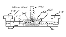
- FIGS. 2A and 2B schematically illustrate the EO region (depletion region of a silicon PN junction) arrangements for the optical modulator according to embodiments of the present invention.
- the cross-sections are taken at a position along the modulator waveguide 103 , such as position C 4 (see FIG. 1A and FIG. 1E ).
- the EO region (between the dashed lines) 208 / 208 ′ has different shapes.
- the optimized location to position the EO region 208 / 208 ′ is always the place where the mode 209 / 209 ′ has the highest intensity so that the optical property changes can have the strongest effect on the optical signal.
- the optical mode 209 / 209 ′ sits in the lower ridge 203 R (corresponding to 103 R in FIG. 1E ) with very little energy penetration into the fin structure 203 F (corresponding to 103 F in FIG. 1E ). This is the reason the EO region 208 / 208 ′ is positioned mainly in the lower ridge 203 R.
- the EO region 208 / 208 ′ is sandwiched by the field source regions 210 / 210 ′.
- the EO region 208 / 208 ′ is the depletion region of the PN junction.
- the field source regions 210 / 210 ′ are N-doped and P-doped silicon layers.
- the area (i.e. size) of the depletion region changes, which in turn changes the phase of the optical mode that propagates inside the waveguide.
- the electric field is vertically oriented inside the electro-optic region perpendicular to the surfaces of the field source regions and vertically across the PN junction interface.
- MZI Mach-Zehnder interferometer
- the EO region 208 / 208 ′ connects to the metal electrodes 211 / 211 ′ through the horizontally arranged field source regions 210 / 210 ′.
- the metal electrodes 211 / 211 ′ are positioned on opposite sides of the waveguide and are electrically connected to the field source regions 210 / 210 ′, which are doped horizontal N+ and P+ layers extending in the direction perpendicular to the light traveling direction in the cross-sectional view as shown in FIGS. 2A and 2B .
- Heavily doped N++ and P++ layers are disposed below the metal electrode 211 to minimize ohmic contact loss. These heavily doped regions are positioned far enough from the lower ridge 203 R that the optical mode cannot “see” the layers. Such arrangement makes the fabrication much easier and maintains the device performances.
- FIGS. 3A-3D schematically illustrate the key process steps of fabricating the optical modulator structure illustrated in FIG. 2A according to an embodiment of the present invention.
- These figures are cross-sectional views taken at a position in the modulator waveguide section 103 , e.g. at C 4 of FIG. 1A , at different processing stages.
- the process begins with a substrate with epitaxial layers. From the bottom to top of the substrate, the layer arrangement is, silicon substrate and SiO 2 buffer layer (not shown in the figures), P+ silicon layer, N+ silicon layer, and intrinsic silicon layer. The thickness of the P+ silicon layer is chosen to make sure the depletion region of the PN junction is positioned where the EO effect should be the strongest.
- the P+ layer doping level is smaller than that of the N+ layer, since holes in the P+ layer show stronger response than the electrons in the N+ layer.
- the typical thicknesses of the P+ and N+ layers are in the range of, but not limited to, 0.1 ⁇ m to 0.3 ⁇ m.
- the total thickness of the P+ and N+ layers is preferably less than the thickness of lower ridge 203 R marked in FIG. 2A to reduce free carrier loss from unnecessarily doped areas. Note that the thickness of the lower ridge 203 R is defined as the distance between the top surface of the lower ridge 203 R (i.e. trench 105 ) and the lower boundary of the P+ silicon region.
- the substrate is under a first etch as shown in FIG. 3A to form a shallow trench 306 , with typical depth in the range of, but not limited to, 0.1 to 0.2 ⁇ m. Only the areas labeled 106 in FIG. 1A are etched in this first etching step.
- the second trench 304 is etched in the next step as shown in FIG. 3B to form the upper ridge of the coupling waveguide.
- the areas labeled 104 , 105 and 106 in FIG. 1A are etched in this second etching step.
- a self-aligned process is used to further etch the trench 305 to form the fin structure of the modulator.
- the areas labeled 105 and 106 in FIG. 1A are etched in this third etching step. As seen in FIG.
- the wider top ridge in FIG. 3B is etched to the narrower top ridge, and the height of the surface 306 (corresponding to area 106 in FIG. 1A ) is now below the boundary between the intrinsic silicon and the N+ silicon.
- the solid horizontal line in the region 203 R indicates the boundary between the intrinsic silicon and the N+ silicon.
- the heavily doped N++ and P++ layers are deposited below the metal contact 311 to finish the key process steps ( FIG. 3D , taken at position C 4 ).
- FIG. 2B is an alternative structure to solve those problems.
- the boundary between the doped N+ and P+ layers is not flat but is higher in a center region within the lower ridge 203 R, and even higher at the center region below the fin structure 203 F.
- the shape of the EO region (depletion region of the PN junction) 208 ′ as indicated by the dashed lines follow the shape of the P+/N+ boundary.
- FIGS. 4A-4D schematically illustrate the key process steps of fabricating the optical modulator structure illustrated in FIG. 2B according to an embodiment of the present invention.
- the process again begins with an epitaxial substrate.
- the difference from FIG. 2A structure is the layer arrangement: only the P+ silicon layer is epitaxial grown in this case.
- the thickness of the P+ layer is chosen to be larger than the thickness of the lower ridge 203 R marked in FIG. 2B , with typical value in the range of, but not limited to, 0.5 ⁇ m to 1.5 ⁇ m depending on the fabrication resolution and the implanting penetration depth.
- the processes begins with a few etching steps shown in FIG. 4A and FIG. 4B , to form the shallow trench 406 (where areas corresponding to areas 106 in FIG.
- the exposed area is preferably asymmetric (the left side is covered with photoresist in this example) to reduce unnecessary capacitance in the unused area.
- the modulator waveguide undergoes an angled N+ implantation (for example but not limited to 45 degree) where the angle points from the outside toward the lateral center of the ridge 403 R.
- the doping level is chosen to compensate the original P+ doping in the upper area of the lower ridge 203 R and form the designed PN junction N+ doping level.
- the implanting depth is chosen to from the depletion region of the PN junction at the mode center area. Due to the angled implantation, the fin structure 203 F is N+ doped.
- the doped fin structure does not introduce more free-carrier loss since only a small portion of the optical mode “sees” the doping in the fin structure 203 F.
- the angled implantation scheme results in a unique upside-down “V” shaped PN junction interface. Such shaped PN junction can compensate the modulation efficiency loss due to the mode center shifting up to the fin structure 203 F.
- the heavily doped N++ and P++ layers are deposited below the metal contact 411 to finish the key process steps ( FIG. 4D ).
Landscapes
- Physics & Mathematics (AREA)
- General Physics & Mathematics (AREA)
- Optics & Photonics (AREA)
- Nonlinear Science (AREA)
- Engineering & Computer Science (AREA)
- Microelectronics & Electronic Packaging (AREA)
- Power Engineering (AREA)
- Electromagnetism (AREA)
- Optical Modulation, Optical Deflection, Nonlinear Optics, Optical Demodulation, Optical Logic Elements (AREA)
Abstract
Description
Claims (12)
Priority Applications (1)
| Application Number | Priority Date | Filing Date | Title |
|---|---|---|---|
| US14/605,802 US9323079B1 (en) | 2015-01-26 | 2015-01-26 | Optical device having electro-optic silicon modulator on large core fin waveguide and method to make the same |
Applications Claiming Priority (1)
| Application Number | Priority Date | Filing Date | Title |
|---|---|---|---|
| US14/605,802 US9323079B1 (en) | 2015-01-26 | 2015-01-26 | Optical device having electro-optic silicon modulator on large core fin waveguide and method to make the same |
Publications (1)
| Publication Number | Publication Date |
|---|---|
| US9323079B1 true US9323079B1 (en) | 2016-04-26 |
Family
ID=55754637
Family Applications (1)
| Application Number | Title | Priority Date | Filing Date |
|---|---|---|---|
| US14/605,802 Active US9323079B1 (en) | 2015-01-26 | 2015-01-26 | Optical device having electro-optic silicon modulator on large core fin waveguide and method to make the same |
Country Status (1)
| Country | Link |
|---|---|
| US (1) | US9323079B1 (en) |
Cited By (8)
| Publication number | Priority date | Publication date | Assignee | Title |
|---|---|---|---|---|
| US9864136B1 (en) * | 2016-08-09 | 2018-01-09 | Globalfoundries Inc. | Non-planar monolithic hybrid optoelectronic structures and methods |
| US20180011347A1 (en) * | 2016-07-06 | 2018-01-11 | Fujikura Ltd. | Optical modulation element, optical modulator, and manufacturing method of optical modulation element |
| US20190170940A1 (en) * | 2015-06-30 | 2019-06-06 | Elenion Technologies, Llc | Integrated on-chip polarizer |
| US10656443B2 (en) | 2017-03-16 | 2020-05-19 | The Trustees Of Dartmouth College | Method and apparatus of surface-incident, plasmon-enhanced multiple quantum well modulators and optical coupling thereon |
| WO2020216917A1 (en) * | 2019-04-24 | 2020-10-29 | University Of Southampton | Photonic chip and method of manufacture |
| CN114624903A (en) * | 2020-12-11 | 2022-06-14 | 马维尔亚洲私人有限公司 | Method for improving modulation efficiency in silicon optical modulator |
| CN115145057A (en) * | 2020-12-07 | 2022-10-04 | 马维尔亚洲私人有限公司 | Multi-doped flat silicon optical modulator |
| CN115685444A (en) * | 2022-11-09 | 2023-02-03 | 希烽光电科技(南京)有限公司 | Compensation doping method of silicon-based electro-optic modulator and silicon-based electro-optic modulator |
Citations (9)
| Publication number | Priority date | Publication date | Assignee | Title |
|---|---|---|---|---|
| US7116853B2 (en) | 2003-08-15 | 2006-10-03 | Luxtera, Inc. | PN diode optical modulators fabricated in rib waveguides |
| US7136544B1 (en) | 2003-08-15 | 2006-11-14 | Luxtera, Inc. | PN diode optical modulators fabricated in strip loaded waveguides |
| US7251408B1 (en) | 2003-08-15 | 2007-07-31 | Luxtera, Inc. | Doping profiles in PN diode optical modulators |
| US7280712B2 (en) | 2005-08-04 | 2007-10-09 | Intel Corporation | Method and apparatus for phase shifiting an optical beam in an optical device |
| US7394948B1 (en) | 2004-06-07 | 2008-07-01 | Kotura, Inc. | High speed optical phase modulator |
| US7747122B2 (en) | 2008-09-30 | 2010-06-29 | Intel Corporation | Method and apparatus for high speed silicon optical modulation using PN diode |
| US8149493B2 (en) | 2008-09-06 | 2012-04-03 | Sifotonics Technologies (Usa) Inc. | Electro-optic silicon modulator |
| US20130188902A1 (en) * | 2010-02-17 | 2013-07-25 | Frederic Gardes | Electro-optic device |
| US20160004104A1 (en) | 2014-07-01 | 2016-01-07 | Laxense Inc. | Silicon optical modulator using asymmetric shallow waveguide and the method to make the same |
-
2015
- 2015-01-26 US US14/605,802 patent/US9323079B1/en active Active
Patent Citations (9)
| Publication number | Priority date | Publication date | Assignee | Title |
|---|---|---|---|---|
| US7116853B2 (en) | 2003-08-15 | 2006-10-03 | Luxtera, Inc. | PN diode optical modulators fabricated in rib waveguides |
| US7136544B1 (en) | 2003-08-15 | 2006-11-14 | Luxtera, Inc. | PN diode optical modulators fabricated in strip loaded waveguides |
| US7251408B1 (en) | 2003-08-15 | 2007-07-31 | Luxtera, Inc. | Doping profiles in PN diode optical modulators |
| US7394948B1 (en) | 2004-06-07 | 2008-07-01 | Kotura, Inc. | High speed optical phase modulator |
| US7280712B2 (en) | 2005-08-04 | 2007-10-09 | Intel Corporation | Method and apparatus for phase shifiting an optical beam in an optical device |
| US8149493B2 (en) | 2008-09-06 | 2012-04-03 | Sifotonics Technologies (Usa) Inc. | Electro-optic silicon modulator |
| US7747122B2 (en) | 2008-09-30 | 2010-06-29 | Intel Corporation | Method and apparatus for high speed silicon optical modulation using PN diode |
| US20130188902A1 (en) * | 2010-02-17 | 2013-07-25 | Frederic Gardes | Electro-optic device |
| US20160004104A1 (en) | 2014-07-01 | 2016-01-07 | Laxense Inc. | Silicon optical modulator using asymmetric shallow waveguide and the method to make the same |
Non-Patent Citations (1)
| Title |
|---|
| U.S. Appl. No. 14/321,376, filed Jul. 1, 2014. |
Cited By (13)
| Publication number | Priority date | Publication date | Assignee | Title |
|---|---|---|---|---|
| US20190170940A1 (en) * | 2015-06-30 | 2019-06-06 | Elenion Technologies, Llc | Integrated on-chip polarizer |
| US10545288B2 (en) * | 2015-06-30 | 2020-01-28 | Elenion Technologies, Llc | Integrated on-chip polarizer |
| US20180011347A1 (en) * | 2016-07-06 | 2018-01-11 | Fujikura Ltd. | Optical modulation element, optical modulator, and manufacturing method of optical modulation element |
| US10151941B2 (en) * | 2016-07-06 | 2018-12-11 | Fujikura Ltd. | Optical modulation element, optical modulator, and manufacturing method of optical modulation element |
| US9864136B1 (en) * | 2016-08-09 | 2018-01-09 | Globalfoundries Inc. | Non-planar monolithic hybrid optoelectronic structures and methods |
| US10656443B2 (en) | 2017-03-16 | 2020-05-19 | The Trustees Of Dartmouth College | Method and apparatus of surface-incident, plasmon-enhanced multiple quantum well modulators and optical coupling thereon |
| WO2020216917A1 (en) * | 2019-04-24 | 2020-10-29 | University Of Southampton | Photonic chip and method of manufacture |
| US20220214498A1 (en) * | 2019-04-24 | 2022-07-07 | University Of Southampton | Photonic chip and method of manufacture |
| US12339493B2 (en) * | 2019-04-24 | 2025-06-24 | University Of Southampton | Photonic chip and method of manufacture |
| CN115145057A (en) * | 2020-12-07 | 2022-10-04 | 马维尔亚洲私人有限公司 | Multi-doped flat silicon optical modulator |
| CN114624903A (en) * | 2020-12-11 | 2022-06-14 | 马维尔亚洲私人有限公司 | Method for improving modulation efficiency in silicon optical modulator |
| CN115685444A (en) * | 2022-11-09 | 2023-02-03 | 希烽光电科技(南京)有限公司 | Compensation doping method of silicon-based electro-optic modulator and silicon-based electro-optic modulator |
| CN115685444B (en) * | 2022-11-09 | 2024-06-11 | 希烽光电科技(南京)有限公司 | Compensation doping method of silicon-based electro-optic modulator and silicon-based electro-optic modulator |
Similar Documents
| Publication | Publication Date | Title |
|---|---|---|
| US9323079B1 (en) | Optical device having electro-optic silicon modulator on large core fin waveguide and method to make the same | |
| US9568750B2 (en) | Hybrid optical modulator | |
| US8532440B2 (en) | Silicon-based electro-optic device | |
| US10955692B2 (en) | Optoelectronic component | |
| US8693811B2 (en) | High data-rate SOI optical modulator including a modified structure for reducing the capacitive effect between doped areas and a substrate | |
| CN102165346B (en) | Method and apparatus for high speed silicon optical modulation using PN diode | |
| US9343638B2 (en) | Electro-optic PN junction modulator formed with a self-aligned process | |
| US9612459B2 (en) | Silicon optical modulator using asymmetric shallow waveguide and the method to make the same | |
| US10151941B2 (en) | Optical modulation element, optical modulator, and manufacturing method of optical modulation element | |
| US20170184883A1 (en) | Dual-junction optical modulator and the method to make the same | |
| US10962812B2 (en) | Electro-optic modulator | |
| CN102763264B (en) | Phase shifter, coupler and methods for their production | |
| CN110325900A (en) | Waveguide Optoelectronic Devices | |
| CN108828797B (en) | Silicon-based electro-absorption modulator and preparation method thereof | |
| WO2010151224A1 (en) | Thin-film solar cell interconnection | |
| US20170214216A1 (en) | Hybrid semiconductor lasers | |
| KR102163885B1 (en) | Electro-absorption optical modulation device and the method of fabricating the same | |
| US8823121B2 (en) | Waveguide photo-detector | |
| US11686991B1 (en) | Silicon optical modulator, method for making the same | |
| CN114391122B (en) | Optoelectronic component and method for producing an optoelectronic component | |
| CN108051972B (en) | Silicon photon modulator with wavelength irrelevant high extinction ratio | |
| US9020312B2 (en) | Connecting channel | |
| Ku et al. | High Speed Mach Zehnder Modulator with Low Series Resistance Phase Shifter Loaded in Traveling Wave Electrode |
Legal Events
| Date | Code | Title | Description |
|---|---|---|---|
| AS | Assignment |
Owner name: LAXENSE INC., CALIFORNIA Free format text: ASSIGNMENT OF ASSIGNORS INTEREST;ASSIGNORS:FENG, NINGNING;SUN, XIAOCHEN;REEL/FRAME:034828/0880 Effective date: 20150126 |
|
| STCF | Information on status: patent grant |
Free format text: PATENTED CASE |
|
| MAFP | Maintenance fee payment |
Free format text: PAYMENT OF MAINTENANCE FEE, 4TH YR, SMALL ENTITY (ORIGINAL EVENT CODE: M2551); ENTITY STATUS OF PATENT OWNER: SMALL ENTITY Year of fee payment: 4 |
|
| AS | Assignment |
Owner name: LEIXINUS, INC., CALIFORNIA Free format text: LICENSE;ASSIGNOR:LAXENSE, INC.;REEL/FRAME:054220/0084 Effective date: 20200919 |
|
| AS | Assignment |
Owner name: LAXENSE, INC., CALIFORNIA Free format text: LICENSE;ASSIGNOR:LEIXINUS, INC.;REEL/FRAME:060739/0626 Effective date: 20220718 |
|
| MAFP | Maintenance fee payment |
Free format text: PAYMENT OF MAINTENANCE FEE, 8TH YR, SMALL ENTITY (ORIGINAL EVENT CODE: M2552); ENTITY STATUS OF PATENT OWNER: SMALL ENTITY Year of fee payment: 8 |