US9312495B2 - Materials for organic electroluminescent devices - Google Patents
Materials for organic electroluminescent devices Download PDFInfo
- Publication number
- US9312495B2 US9312495B2 US13/823,401 US201113823401A US9312495B2 US 9312495 B2 US9312495 B2 US 9312495B2 US 201113823401 A US201113823401 A US 201113823401A US 9312495 B2 US9312495 B2 US 9312495B2
- Authority
- US
- United States
- Prior art keywords
- atoms
- group
- formula
- radicals
- organic
- Prior art date
- Legal status (The legal status is an assumption and is not a legal conclusion. Google has not performed a legal analysis and makes no representation as to the accuracy of the status listed.)
- Active, expires
Links
- 0 *C.*C.*C.CC.CN(C)[Ar]C1=C/C2=C(\C=C/1)C1=C(C=CC=C1)C21C2=C(C=CC=C2)C2=C1C=CC=C2 Chemical compound *C.*C.*C.CC.CN(C)[Ar]C1=C/C2=C(\C=C/1)C1=C(C=CC=C1)C21C2=C(C=CC=C2)C2=C1C=CC=C2 0.000 description 37
- ONCCVJKFWKAZAE-UHFFFAOYSA-N BrC1=C/C2=C(\C=C/1)C1=CC=CC=C1C21C2=C(C=CC=C2)C2=C1C=CC=C2 Chemical compound BrC1=C/C2=C(\C=C/1)C1=CC=CC=C1C21C2=C(C=CC=C2)C2=C1C=CC=C2 ONCCVJKFWKAZAE-UHFFFAOYSA-N 0.000 description 16
- LQBFKTGSDZZFEG-UHFFFAOYSA-N CC1(C)C2=CC=CC=C2C2=CC=C(NC3=C/C4=C(\C=C/3)C3=CC=CC=C3C43C4=C(C=CC=C4)C4=C3C=CC=C4)C=C21 Chemical compound CC1(C)C2=CC=CC=C2C2=CC=C(NC3=C/C4=C(\C=C/3)C3=CC=CC=C3C43C4=C(C=CC=C4)C4=C3C=CC=C4)C=C21 LQBFKTGSDZZFEG-UHFFFAOYSA-N 0.000 description 9
- MBHPOBSZPYEADG-UHFFFAOYSA-N CC1(C)C2=CC(Br)=CC=C2C2=C1C=CC=C2 Chemical compound CC1(C)C2=CC(Br)=CC=C2C2=C1C=CC=C2 MBHPOBSZPYEADG-UHFFFAOYSA-N 0.000 description 8
- SXOUNESKHJIXNK-UHFFFAOYSA-N CC1(C)C2=CC=CC(Br)=C2C2=C1C=CC=C2 Chemical compound CC1(C)C2=CC=CC(Br)=C2C2=C1C=CC=C2 SXOUNESKHJIXNK-UHFFFAOYSA-N 0.000 description 5
- TWBPWBPGNQWFSJ-UHFFFAOYSA-N NC1=CC=CC=C1C1=CC=CC=C1 Chemical compound NC1=CC=CC=C1C1=CC=CC=C1 TWBPWBPGNQWFSJ-UHFFFAOYSA-N 0.000 description 5
- PKJBWOWQJHHAHG-UHFFFAOYSA-N BrC1=CC=C(C2=CC=CC=C2)C=C1 Chemical compound BrC1=CC=C(C2=CC=CC=C2)C=C1 PKJBWOWQJHHAHG-UHFFFAOYSA-N 0.000 description 4
- GMOUUEZVFJJUDU-UHFFFAOYSA-N C1=CC=C(C2=C(NC3=CC=C(C4=C/C5=C(\C=C/4)C4=CC=CC=C4C54C5=C(C=CC=C5)C5=C4C=CC=C5)C=C3)C=CC=C2)C=C1 Chemical compound C1=CC=C(C2=C(NC3=CC=C(C4=C/C5=C(\C=C/4)C4=CC=CC=C4C54C5=C(C=CC=C5)C5=C4C=CC=C5)C=C3)C=CC=C2)C=C1 GMOUUEZVFJJUDU-UHFFFAOYSA-N 0.000 description 4
- UMUHBIQPUIPIOH-UHFFFAOYSA-N C1=CC=C(C2=CC(C3=CC=CC=C3)=C(NC3=C/C4=C(\C=C/3)C3=CC=CC=C3C43C4=C(C=CC=C4)C4=C3C=CC=C4)C=C2)C=C1 Chemical compound C1=CC=C(C2=CC(C3=CC=CC=C3)=C(NC3=C/C4=C(\C=C/3)C3=CC=CC=C3C43C4=C(C=CC=C4)C4=C3C=CC=C4)C=C2)C=C1 UMUHBIQPUIPIOH-UHFFFAOYSA-N 0.000 description 4
- MTYGHSICPWZTQY-UHFFFAOYSA-N C1=CC=C(C2=CC=C(NC3=C/C4=C(\C=C/3)C3=CC=CC=C3C43C4=C(C=CC=C4)C4=C3C=CC=C4)C=C2)C=C1 Chemical compound C1=CC=C(C2=CC=C(NC3=C/C4=C(\C=C/3)C3=CC=CC=C3C43C4=C(C=CC=C4)C4=C3C=CC=C4)C=C2)C=C1 MTYGHSICPWZTQY-UHFFFAOYSA-N 0.000 description 4
- VECLPBKDHAALGQ-UHFFFAOYSA-N CC1(C)C2=CC=C(Br)C=C2C2=C1C=CC=C2 Chemical compound CC1(C)C2=CC=C(Br)C=C2C2=C1C=CC=C2 VECLPBKDHAALGQ-UHFFFAOYSA-N 0.000 description 4
- LKXROGPOVQMZOJ-UHFFFAOYSA-N CC1(C)C2=CC=CC=C2C2=CC(N(C3=CC=CC(C4=CC=CC=C4)=C3)C3=CC4=C(C=C3)C3=C(C=CC=C3)C43C4=C(C=CC=C4)C4=C3C=CC=C4)=CC=C21 Chemical compound CC1(C)C2=CC=CC=C2C2=CC(N(C3=CC=CC(C4=CC=CC=C4)=C3)C3=CC4=C(C=C3)C3=C(C=CC=C3)C43C4=C(C=CC=C4)C4=C3C=CC=C4)=CC=C21 LKXROGPOVQMZOJ-UHFFFAOYSA-N 0.000 description 4
- IWLOXVWEHNKUSY-UHFFFAOYSA-N BrC1=CC=C(C2=C/C3=C(\C=C/2)C2=CC=CC=C2C32C3=C(C=CC=C3)C3=C2C=CC=C3)C=C1 Chemical compound BrC1=CC=C(C2=C/C3=C(\C=C/2)C2=CC=CC=C2C32C3=C(C=CC=C3)C3=C2C=CC=C3)C=C1 IWLOXVWEHNKUSY-UHFFFAOYSA-N 0.000 description 3
- FPXNYQAPKKRADH-UHFFFAOYSA-N C1=CC2=C(C=C1)C1(C3=CC(N(C4=CC=C5C(=C4)C4(C6=C5C=CC=C6)C5=C(C=CC=C5)C5=C4C=CC=C5)C4=CC=C5C(=C4)C4(C6=C5C=CC=C6)C5=C(C=CC=C5)C5=C4C=CC=C5)=CC=C32)C2=C(C=CC=C2)C2=C1C=CC=C2 Chemical compound C1=CC2=C(C=C1)C1(C3=CC(N(C4=CC=C5C(=C4)C4(C6=C5C=CC=C6)C5=C(C=CC=C5)C5=C4C=CC=C5)C4=CC=C5C(=C4)C4(C6=C5C=CC=C6)C5=C(C=CC=C5)C5=C4C=CC=C5)=CC=C32)C2=C(C=CC=C2)C2=C1C=CC=C2 FPXNYQAPKKRADH-UHFFFAOYSA-N 0.000 description 3
- HGKFUGDYVSGRAA-UHFFFAOYSA-N C1=CC=C(C2=CC=C(N(C3=CC=C(C4=CC=CC=C4)C=C3)C3=CC4=C(C=C3)C3=C(C=CC=C3)C43C4=C(C=CC=C4)C4=C3C=CC=C4)C=C2)C=C1 Chemical compound C1=CC=C(C2=CC=C(N(C3=CC=C(C4=CC=CC=C4)C=C3)C3=CC4=C(C=C3)C3=C(C=CC=C3)C43C4=C(C=CC=C4)C4=C3C=CC=C4)C=C2)C=C1 HGKFUGDYVSGRAA-UHFFFAOYSA-N 0.000 description 3
- PMQVURFBYNIWEJ-UHFFFAOYSA-N C1=CC=C2C(=C1)C1=CC=CC=C1C21C2=CC=CC=C2C2=CC=C(NC3=C/C4=C(\C=C/3)C3=CC=CC=C3C43C4=C(C=CC=C4)C4=C3C=CC=C4)C=C21 Chemical compound C1=CC=C2C(=C1)C1=CC=CC=C1C21C2=CC=CC=C2C2=CC=C(NC3=C/C4=C(\C=C/3)C3=CC=CC=C3C43C4=C(C=CC=C4)C4=C3C=CC=C4)C=C21 PMQVURFBYNIWEJ-UHFFFAOYSA-N 0.000 description 3
- OCASTJYUPOMTIX-UHFFFAOYSA-N CC1(C)C2=CC=CC=C2C2=CC=C(N(C3=CC4=C(C=C3)C3=C(C=CC=C3)C43C4=C(C=CC(C5=CC=CC=C5)=C4)C4=C3C=C(C3=CC=CC=C3)C=C4)C3=CC=CC=C3C3=CC=CC=C3)C=C21 Chemical compound CC1(C)C2=CC=CC=C2C2=CC=C(N(C3=CC4=C(C=C3)C3=C(C=CC=C3)C43C4=C(C=CC(C5=CC=CC=C5)=C4)C4=C3C=C(C3=CC=CC=C3)C=C4)C3=CC=CC=C3C3=CC=CC=C3)C=C21 OCASTJYUPOMTIX-UHFFFAOYSA-N 0.000 description 3
- RRFYJFKAFGEXSL-UHFFFAOYSA-N CC1=CC(C2=CC=CC=C2)=CC(C)=C1NC1=C/C2=C(\C=C/1)C1=CC=CC=C1C21C2=C(C=CC=C2)C2=C1C=CC=C2 Chemical compound CC1=CC(C2=CC=CC=C2)=CC(C)=C1NC1=C/C2=C(\C=C/1)C1=CC=CC=C1C21C2=C(C=CC=C2)C2=C1C=CC=C2 RRFYJFKAFGEXSL-UHFFFAOYSA-N 0.000 description 3
- UCFDALUXSMNRHK-UHFFFAOYSA-N NC1=C/C2=C(\C=C/1)C1=CC=CC=C1C21C2=C(C=CC=C2)C2=C1C=CC=C2 Chemical compound NC1=C/C2=C(\C=C/1)C1=CC=CC=C1C21C2=C(C=CC=C2)C2=C1C=CC=C2 UCFDALUXSMNRHK-UHFFFAOYSA-N 0.000 description 3
- USYQKCQEVBFJRP-UHFFFAOYSA-N BrC1=CC(C2=CC=CC=C2)=CC=C1 Chemical compound BrC1=CC(C2=CC=CC=C2)=CC=C1 USYQKCQEVBFJRP-UHFFFAOYSA-N 0.000 description 2
- JLBXMPBCAYRQSZ-UHFFFAOYSA-N BrC1=CC=C2C(=C1)C1(CCCCC1)C1=C2C=CC=C1 Chemical compound BrC1=CC=C2C(=C1)C1(CCCCC1)C1=C2C=CC=C1 JLBXMPBCAYRQSZ-UHFFFAOYSA-N 0.000 description 2
- LMHBCXMDEMSIHC-UHFFFAOYSA-N C1=CC=C(C2=C(NC3=C/C4=C(\C=C/3)C3=CC=CC=C3C43C4=C(C=CC=C4)C4=C3C=CC=C4)C=CC=C2)C=C1 Chemical compound C1=CC=C(C2=C(NC3=C/C4=C(\C=C/3)C3=CC=CC=C3C43C4=C(C=CC=C4)C4=C3C=CC=C4)C=CC=C2)C=C1 LMHBCXMDEMSIHC-UHFFFAOYSA-N 0.000 description 2
- DBLXXZVQFIARJQ-UHFFFAOYSA-N C1=CC=C(C2=CC(C3=CC=CC=C3)=CC(C3=CC4=C(C=C3)C3=C(C=C(N(C5=CC=CC(C6=CC=CC=C6)=C5)C5=CC=CC=C5C5=CC=CC=C5)C=C3)C43C4=C(C=CC=C4)C4=C3C=CC=C4)=C2)C=C1 Chemical compound C1=CC=C(C2=CC(C3=CC=CC=C3)=CC(C3=CC4=C(C=C3)C3=C(C=C(N(C5=CC=CC(C6=CC=CC=C6)=C5)C5=CC=CC=C5C5=CC=CC=C5)C=C3)C43C4=C(C=CC=C4)C4=C3C=CC=C4)=C2)C=C1 DBLXXZVQFIARJQ-UHFFFAOYSA-N 0.000 description 2
- CCPAAQATLGLTKH-UHFFFAOYSA-N C1=CC=C(C2=CC=C(N(C3=CC4=C(C=C3)C3=C(C=CC=C3)C43C4=C(C=CC=C4)C4=C3C=CC=C4)C3=C4SC5=CC=CC=C5C4=CC=C3)C=C2)C=C1 Chemical compound C1=CC=C(C2=CC=C(N(C3=CC4=C(C=C3)C3=C(C=CC=C3)C43C4=C(C=CC=C4)C4=C3C=CC=C4)C3=C4SC5=CC=CC=C5C4=CC=C3)C=C2)C=C1 CCPAAQATLGLTKH-UHFFFAOYSA-N 0.000 description 2
- DUNYSYGAIRCTLH-UHFFFAOYSA-N C1=CC=C(C2=CC=C(N(C3=CC4=C(C=C3)C3=C(C=CC=C3)C43C4=C(C=CC=C4)C4=C3C=CC=C4)C3=CC=C(C4=CC=CC=C4)C=C3C3=CC=CC=C3)C=C2)C=C1 Chemical compound C1=CC=C(C2=CC=C(N(C3=CC4=C(C=C3)C3=C(C=CC=C3)C43C4=C(C=CC=C4)C4=C3C=CC=C4)C3=CC=C(C4=CC=CC=C4)C=C3C3=CC=CC=C3)C=C2)C=C1 DUNYSYGAIRCTLH-UHFFFAOYSA-N 0.000 description 2
- WXAIEIRYBSKHDP-UHFFFAOYSA-N C1=CC=C(C2=CC=C(N(C3=CC=C(C4=CC=CC=C4)C=C3)C3=CC=C(C4=CC=C(N(C5=CC=C(C6=CC=CC=C6)C=C5)C5=CC=C(C6=CC=CC=C6)C=C5)C=C4)C=C3)C=C2)C=C1 Chemical compound C1=CC=C(C2=CC=C(N(C3=CC=C(C4=CC=CC=C4)C=C3)C3=CC=C(C4=CC=C(N(C5=CC=C(C6=CC=CC=C6)C=C5)C5=CC=C(C6=CC=CC=C6)C=C5)C=C4)C=C3)C=C2)C=C1 WXAIEIRYBSKHDP-UHFFFAOYSA-N 0.000 description 2
- PFBNDRAGJOZPOQ-UHFFFAOYSA-N C1=CC=C(C2=CC=CC=C2N(C2=CC=C3C4=CC=CC=C4C4(C5=CC=CC=C5C5=CC=CC=C54)C3=C2)C2=C/C3=C(\C=C/2)C2=CC=CC=C2C32C3=C(C=CC=C3)C3=C2C=CC=C3)C=C1 Chemical compound C1=CC=C(C2=CC=CC=C2N(C2=CC=C3C4=CC=CC=C4C4(C5=CC=CC=C5C5=CC=CC=C54)C3=C2)C2=C/C3=C(\C=C/2)C2=CC=CC=C2C32C3=C(C=CC=C3)C3=C2C=CC=C3)C=C1 PFBNDRAGJOZPOQ-UHFFFAOYSA-N 0.000 description 2
- UELRIHMQPRPDQQ-UHFFFAOYSA-N C1=CC=C(C2=CC=CC=C2N(C2=CC=C3C4=CC=CC=C4C4(CCCC4)C3=C2)C2=CC3=C(C=C2)C2=C(C=CC=C2)C32C3=C(C=CC=C3)C3=C2C=CC=C3)C=C1 Chemical compound C1=CC=C(C2=CC=CC=C2N(C2=CC=C3C4=CC=CC=C4C4(CCCC4)C3=C2)C2=CC3=C(C=C2)C2=C(C=CC=C2)C32C3=C(C=CC=C3)C3=C2C=CC=C3)C=C1 UELRIHMQPRPDQQ-UHFFFAOYSA-N 0.000 description 2
- DDCDQEZFMORVDD-UHFFFAOYSA-N C1=CC=C(C2=CC=CC=C2N(C2=CC=C3C4=CC=CC=C4C4(CCCCC4)C3=C2)C2=CC3=C(C=C2)C2=C(C=CC=C2)C32C3=C(C=CC=C3)C3=C2C=CC=C3)C=C1 Chemical compound C1=CC=C(C2=CC=CC=C2N(C2=CC=C3C4=CC=CC=C4C4(CCCCC4)C3=C2)C2=CC3=C(C=C2)C2=C(C=CC=C2)C32C3=C(C=CC=C3)C3=C2C=CC=C3)C=C1 DDCDQEZFMORVDD-UHFFFAOYSA-N 0.000 description 2
- GHARGEZMXCAUIV-UHFFFAOYSA-N C1=CC=C(C2=CC=CC=C2N(C2=CC=C3OC4=CC=CC=C4C3=C2)C2=CC3=C(C=C2)C2=C(C=CC=C2)C32C3=C(C=CC=C3)C3=C2C=CC=C3)C=C1 Chemical compound C1=CC=C(C2=CC=CC=C2N(C2=CC=C3OC4=CC=CC=C4C3=C2)C2=CC3=C(C=C2)C2=C(C=CC=C2)C32C3=C(C=CC=C3)C3=C2C=CC=C3)C=C1 GHARGEZMXCAUIV-UHFFFAOYSA-N 0.000 description 2
- MNOOQOKNGLGWFM-UHFFFAOYSA-N C1=CC=C(C2=CC=CC=C2N(C2=CC=C3SC4=CC=CC=C4C3=C2)C2=CC3=C(C=C2)C2=C(C=CC=C2)C32C3=C(C=CC=C3)C3=C2C=CC=C3)C=C1 Chemical compound C1=CC=C(C2=CC=CC=C2N(C2=CC=C3SC4=CC=CC=C4C3=C2)C2=CC3=C(C=C2)C2=C(C=CC=C2)C32C3=C(C=CC=C3)C3=C2C=CC=C3)C=C1 MNOOQOKNGLGWFM-UHFFFAOYSA-N 0.000 description 2
- HVQVQYSRJHFRHT-UHFFFAOYSA-N C1=CC=C(N(C2=CC=C3C(=C2)C2=CC=CC=C2C3(C2=CC=CC=C2)C2=CC=CC=C2)C2=CC3=C(C=C2)C2=C(C=CC=C2)C32C3=C(C=CC=C3)C3=C2C=CC=C3)C=C1 Chemical compound C1=CC=C(N(C2=CC=C3C(=C2)C2=CC=CC=C2C3(C2=CC=CC=C2)C2=CC=CC=C2)C2=CC3=C(C=C2)C2=C(C=CC=C2)C32C3=C(C=CC=C3)C3=C2C=CC=C3)C=C1 HVQVQYSRJHFRHT-UHFFFAOYSA-N 0.000 description 2
- DXOFPZUCCHUPOB-UHFFFAOYSA-N C1=CC=C(N(C2=CC=CC=C2)C2=C/C3=C(\C=C/2)C2=C(C=CC=C2)C32C3=C(C=CC=C3)C3=C2C=CC=C3)C=C1.CC1=CC=C(N(C2=CC=C(C)C=C2)C2=C/C3=C(\C=C/2)C2=C(C=CC=C2)C32C3=C(C=CC=C3)C3=C2C=CC=C3)C=C1.OC[H]C1=CC2=C(C=C1)C1=C(/C=C(N(C3=CC=CC=C3)C3=CC=CC=C3)\C=C/1)C21C2=C(C=CC=C2)C2=C1C=CC=C2.[C-]#[N+]C1=CC2=C(C=C1)C1=C(/C=C(N(C3=CC=CC=C3)C3=CC=CC=C3)\C=C/1)C21C2=C(C=CC=C2)C2=C1C=CC=C2.[C-]#[N+]C1=CC2=C(C=C1)C1=C(C=C(C#N)C=C1)C21C2=C(C=CC=C2)C2=C1/C=C(N(C1=CC=CC=C1)C1=CC=CC=C1)\C=C/2 Chemical compound C1=CC=C(N(C2=CC=CC=C2)C2=C/C3=C(\C=C/2)C2=C(C=CC=C2)C32C3=C(C=CC=C3)C3=C2C=CC=C3)C=C1.CC1=CC=C(N(C2=CC=C(C)C=C2)C2=C/C3=C(\C=C/2)C2=C(C=CC=C2)C32C3=C(C=CC=C3)C3=C2C=CC=C3)C=C1.OC[H]C1=CC2=C(C=C1)C1=C(/C=C(N(C3=CC=CC=C3)C3=CC=CC=C3)\C=C/1)C21C2=C(C=CC=C2)C2=C1C=CC=C2.[C-]#[N+]C1=CC2=C(C=C1)C1=C(/C=C(N(C3=CC=CC=C3)C3=CC=CC=C3)\C=C/1)C21C2=C(C=CC=C2)C2=C1C=CC=C2.[C-]#[N+]C1=CC2=C(C=C1)C1=C(C=C(C#N)C=C1)C21C2=C(C=CC=C2)C2=C1/C=C(N(C1=CC=CC=C1)C1=CC=CC=C1)\C=C/2 DXOFPZUCCHUPOB-UHFFFAOYSA-N 0.000 description 2
- VOZBMWWMIQGZGM-UHFFFAOYSA-N C1=CC=C(N2C(C3=CC=C(C4=CC=C5C(=C4)C(C4=CC=C6C=CC=CC6=C4)=C4C=CC=CC4=C5C4=CC5=CC=CC=C5C=C4)C=C3)=NC3=C2/C=C\C=C/3)C=C1 Chemical compound C1=CC=C(N2C(C3=CC=C(C4=CC=C5C(=C4)C(C4=CC=C6C=CC=CC6=C4)=C4C=CC=CC4=C5C4=CC5=CC=CC=C5C=C4)C=C3)=NC3=C2/C=C\C=C/3)C=C1 VOZBMWWMIQGZGM-UHFFFAOYSA-N 0.000 description 2
- SRBWSVRIYDVORV-UHFFFAOYSA-N C1=CC=C2C(=C1)C=CC=C2N(C1=CC=C(C2=CC3=C(C=C2)C2=C(C=CC=C2)C32C3=C(C=CC=C3)C3=C2C=CC=C3)C=C1)C1=CC=CC2=CC=CC=C21 Chemical compound C1=CC=C2C(=C1)C=CC=C2N(C1=CC=C(C2=CC3=C(C=C2)C2=C(C=CC=C2)C32C3=C(C=CC=C3)C3=C2C=CC=C3)C=C1)C1=CC=CC2=CC=CC=C21 SRBWSVRIYDVORV-UHFFFAOYSA-N 0.000 description 2
- KOIMQVYJNUKSOQ-UHFFFAOYSA-N C1=CC=C2C(=C1)OC1=C(C=CC=C1)N2C1=CC2=C(C=C1)C1=C(C=CC=C1)C21C2=C(C=CC=C2)C2=C1C=CC=C2 Chemical compound C1=CC=C2C(=C1)OC1=C(C=CC=C1)N2C1=CC2=C(C=C1)C1=C(C=CC=C1)C21C2=C(C=CC=C2)C2=C1C=CC=C2 KOIMQVYJNUKSOQ-UHFFFAOYSA-N 0.000 description 2
- YOGPJFSYRIXXKO-UHFFFAOYSA-N CC(C)(C)C1=CC2=C(C=C1)C1=C(C=C(C(C)(C)C)C=C1)C21C2=C(C=CC=C2)C2=C1C=C(N(C1=CC=C3C4=CC=CC=C4C(C)(C)C3=C1)C1=CC=CC=C1C1=CC=CC=C1)C=C2 Chemical compound CC(C)(C)C1=CC2=C(C=C1)C1=C(C=C(C(C)(C)C)C=C1)C21C2=C(C=CC=C2)C2=C1C=C(N(C1=CC=C3C4=CC=CC=C4C(C)(C)C3=C1)C1=CC=CC=C1C1=CC=CC=C1)C=C2 YOGPJFSYRIXXKO-UHFFFAOYSA-N 0.000 description 2
- BJNIYBJYXQRWPP-UHFFFAOYSA-N CC(C)(C)C1=CC2=C(C=C1)C1=C(C=C(N3C4=CC=CC=C4OC4=C3C=CC=C4)C=C1)C21C2=C(C=CC=C2)C2=C1C=CC=C2 Chemical compound CC(C)(C)C1=CC2=C(C=C1)C1=C(C=C(N3C4=CC=CC=C4OC4=C3C=CC=C4)C=C1)C21C2=C(C=CC=C2)C2=C1C=CC=C2 BJNIYBJYXQRWPP-UHFFFAOYSA-N 0.000 description 2
- QMOIWFTVDUITBA-UHFFFAOYSA-N CC(C)(C)C1=CC2=C(C=C1)C1=C(C=C(N3C4=CC=CC=C4SC4=C3C=CC=C4)C=C1)C21C2=C(C=CC(C(C)(C)C)=C2)C2=C1C=C(C(C)(C)C)C=C2 Chemical compound CC(C)(C)C1=CC2=C(C=C1)C1=C(C=C(N3C4=CC=CC=C4SC4=C3C=CC=C4)C=C1)C21C2=C(C=CC(C(C)(C)C)=C2)C2=C1C=C(C(C)(C)C)C=C2 QMOIWFTVDUITBA-UHFFFAOYSA-N 0.000 description 2
- WRCYEBMHTVCQFF-UHFFFAOYSA-N CC1(C)C2=C(C=CC=C2)C2=C1C=C(N(C1=CC(C3=CC=CC=C3)=CC(C3=CC=CC=C3)=C1)C1=CC3=C(C=C1)C1=C(C=CC=C1)C31C3=C(C=CC=C3)C3=C1C=CC=C3)C=C2 Chemical compound CC1(C)C2=C(C=CC=C2)C2=C1C=C(N(C1=CC(C3=CC=CC=C3)=CC(C3=CC=CC=C3)=C1)C1=CC3=C(C=C1)C1=C(C=CC=C1)C31C3=C(C=CC=C3)C3=C1C=CC=C3)C=C2 WRCYEBMHTVCQFF-UHFFFAOYSA-N 0.000 description 2
- SSQNLXRWWBAOOY-UHFFFAOYSA-N CC1(C)C2=C(C=CC=C2)C2=C1C=C(N(C1=CC=C(C#N)C=C1)C1=CC3=C(C=C1)C1=C(C=CC=C1)C31C3=C(C=CC=C3)C3=C1C=CC=C3)C=C2 Chemical compound CC1(C)C2=C(C=CC=C2)C2=C1C=C(N(C1=CC=C(C#N)C=C1)C1=CC3=C(C=C1)C1=C(C=CC=C1)C31C3=C(C=CC=C3)C3=C1C=CC=C3)C=C2 SSQNLXRWWBAOOY-UHFFFAOYSA-N 0.000 description 2
- ORDPFWUSANFTPJ-UHFFFAOYSA-N CC1(C)C2=C(C=CC=C2)C2=C1C=C(N(C1=CC=C(C3=CC(C4=CC=CC=C4)=CC(C4=CC=CC=C4)=C3)C=C1)C1=C3C=CC=CC3=C(C3=CC4=C(C=C3)C3=C(C=CC=C3)C43C4=C(C=CC=C4)C4=C3C=CC=C4)C=C1)C=C2 Chemical compound CC1(C)C2=C(C=CC=C2)C2=C1C=C(N(C1=CC=C(C3=CC(C4=CC=CC=C4)=CC(C4=CC=CC=C4)=C3)C=C1)C1=C3C=CC=CC3=C(C3=CC4=C(C=C3)C3=C(C=CC=C3)C43C4=C(C=CC=C4)C4=C3C=CC=C4)C=C1)C=C2 ORDPFWUSANFTPJ-UHFFFAOYSA-N 0.000 description 2
- JVTKSCKBFOLWRG-UHFFFAOYSA-N CC1(C)C2=C(C=CC=C2)C2=C1C=C(N(C1=CC=C(C3=CC=C(C#N)C=C3)C=C1)C1=CC3=C(C=C1)C1=C(C=CC=C1)C31C3=C(C=CC=C3)C3=C1C=CC=C3)C=C2 Chemical compound CC1(C)C2=C(C=CC=C2)C2=C1C=C(N(C1=CC=C(C3=CC=C(C#N)C=C3)C=C1)C1=CC3=C(C=C1)C1=C(C=CC=C1)C31C3=C(C=CC=C3)C3=C1C=CC=C3)C=C2 JVTKSCKBFOLWRG-UHFFFAOYSA-N 0.000 description 2
- KMZUUSFWPQLMQE-UHFFFAOYSA-N CC1(C)C2=C(C=CC=C2)C2=CC=CC(Br)=C21 Chemical compound CC1(C)C2=C(C=CC=C2)C2=CC=CC(Br)=C21 KMZUUSFWPQLMQE-UHFFFAOYSA-N 0.000 description 2
- MOEZERMQAXFLOX-UHFFFAOYSA-N CC1(C)C2=CC(C3=CC=CC=C3)=CC=C2N(C2=CC3=C(C=C2)C2=C(C=CC=C2)C32C3=C(C=CC=C3)C3=C2C=CC=C3)C2=C1C=C(C1=CC=CC=C1)C=C2 Chemical compound CC1(C)C2=CC(C3=CC=CC=C3)=CC=C2N(C2=CC3=C(C=C2)C2=C(C=CC=C2)C32C3=C(C=CC=C3)C3=C2C=CC=C3)C2=C1C=C(C1=CC=CC=C1)C=C2 MOEZERMQAXFLOX-UHFFFAOYSA-N 0.000 description 2
- KXLHWCRLENTMCQ-UHFFFAOYSA-N CC1(C)C2=CC(C3=CC=CC=C3)=CC=C2N(C2=CC=C(C3=CC=CC=C3)C=C2)C2=CC=C(C3=CC4=C(C=C3)C3=C(C=CC=C3)C43C4=C(C=CC=C4)C4=C3C=CC=C4)C=C21 Chemical compound CC1(C)C2=CC(C3=CC=CC=C3)=CC=C2N(C2=CC=C(C3=CC=CC=C3)C=C2)C2=CC=C(C3=CC4=C(C=C3)C3=C(C=CC=C3)C43C4=C(C=CC=C4)C4=C3C=CC=C4)C=C21 KXLHWCRLENTMCQ-UHFFFAOYSA-N 0.000 description 2
- YQIQKTOKMDHBSP-UHFFFAOYSA-N CC1(C)C2=CC=CC=C2C2=C1C=C1C(=C2)C2=C(C=CC=C2)N1C1=NC(C2=CC=CC=C2)=NC(C2=CC=CC=C2)=N1 Chemical compound CC1(C)C2=CC=CC=C2C2=C1C=C1C(=C2)C2=C(C=CC=C2)N1C1=NC(C2=CC=CC=C2)=NC(C2=CC=CC=C2)=N1 YQIQKTOKMDHBSP-UHFFFAOYSA-N 0.000 description 2
- TUFSDXBBNDRADV-UHFFFAOYSA-N CC1(C)C2=CC=CC=C2C2=C1C=CC(N(C1=CC3=C(C=C1)C1=C(C=CC=C1)C31C3=C(C=CC=C3)C3=C1C=CC=C3)C1=CC=CC=C1C1=CC=CC=C1)=C2 Chemical compound CC1(C)C2=CC=CC=C2C2=C1C=CC(N(C1=CC3=C(C=C1)C1=C(C=CC=C1)C31C3=C(C=CC=C3)C3=C1C=CC=C3)C1=CC=CC=C1C1=CC=CC=C1)=C2 TUFSDXBBNDRADV-UHFFFAOYSA-N 0.000 description 2
- SWLYPNCGTCTYBW-UHFFFAOYSA-N CC1(C)C2=CC=CC=C2C2=C1C=CC(N(C1=CC=C(C3=CC=CC=C3)C=C1)C1=CC3=C(C=C1)C1=C(C=CC=C1)C31C3=C(C=CC=C3)C3=C1C=CC=C3)=C2 Chemical compound CC1(C)C2=CC=CC=C2C2=C1C=CC(N(C1=CC=C(C3=CC=CC=C3)C=C1)C1=CC3=C(C=C1)C1=C(C=CC=C1)C31C3=C(C=CC=C3)C3=C1C=CC=C3)=C2 SWLYPNCGTCTYBW-UHFFFAOYSA-N 0.000 description 2
- VIJVNNFKXRKJJM-UHFFFAOYSA-N CC1(C)C2=CC=CC=C2C2=CC=C(N(C3=CC4=C(C=C3)C3=C(C=CC=C3)C43C4=C(C=CC=C4)C4=C3C=CC=C4)C3=CC=C(C4=CC=CC=C4)C=C3C3=CC=CC=C3)C=C21 Chemical compound CC1(C)C2=CC=CC=C2C2=CC=C(N(C3=CC4=C(C=C3)C3=C(C=CC=C3)C43C4=C(C=CC=C4)C4=C3C=CC=C4)C3=CC=C(C4=CC=CC=C4)C=C3C3=CC=CC=C3)C=C21 VIJVNNFKXRKJJM-UHFFFAOYSA-N 0.000 description 2
- RPRCVCFYQHSPED-UHFFFAOYSA-N CC1(C)C2=CC=CC=C2C2=CC=C(N(C3=CC4=C(C=C3)C3=C(C=CC=C3)C43C4=C(C=CC=C4)C4=C3C=CC=C4)C3=CC=CC=C3C3=CC=CC=C3)C=C21 Chemical compound CC1(C)C2=CC=CC=C2C2=CC=C(N(C3=CC4=C(C=C3)C3=C(C=CC=C3)C43C4=C(C=CC=C4)C4=C3C=CC=C4)C3=CC=CC=C3C3=CC=CC=C3)C=C21 RPRCVCFYQHSPED-UHFFFAOYSA-N 0.000 description 2
- VJPYNOCTTLZZLN-UHFFFAOYSA-N CC1(C)C2=CC=CC=C2C2=CC=C(N(C3=CC=C(C4=CC=CC=C4)C=C3)C3=CC4=C(C=C3)C3=C(C=CC=C3)C43C4=C(C=CC=C4)C4=C3C=CC=C4)C=C21 Chemical compound CC1(C)C2=CC=CC=C2C2=CC=C(N(C3=CC=C(C4=CC=CC=C4)C=C3)C3=CC4=C(C=C3)C3=C(C=CC=C3)C43C4=C(C=CC=C4)C4=C3C=CC=C4)C=C21 VJPYNOCTTLZZLN-UHFFFAOYSA-N 0.000 description 2
- GZGZFJSOXHNQGX-UHFFFAOYSA-N CC1(C)C2=CC=CC=C2C2=CC=C(N(C3=CC=CC(C4=CC=CC=C4)=C3)C3=CC4=C(C=C3)C3=C(C=CC=C3)C43C4=C(C=CC=C4)C4=C3C=CC=C4)C=C21 Chemical compound CC1(C)C2=CC=CC=C2C2=CC=C(N(C3=CC=CC(C4=CC=CC=C4)=C3)C3=CC4=C(C=C3)C3=C(C=CC=C3)C43C4=C(C=CC=C4)C4=C3C=CC=C4)C=C21 GZGZFJSOXHNQGX-UHFFFAOYSA-N 0.000 description 2
- ZBAWUPLYLJIVIK-UHFFFAOYSA-N CC1(C)C2=CC=CC=C2N(C2=CC3=C(C=C2)C2=C(C=CC=C2)C32C3=C(C=CC=C3)C3=C2C=CC=C3)C2=C1C=CC=C2 Chemical compound CC1(C)C2=CC=CC=C2N(C2=CC3=C(C=C2)C2=C(C=CC=C2)C32C3=C(C=CC=C3)C3=C2C=CC=C3)C2=C1C=CC=C2 ZBAWUPLYLJIVIK-UHFFFAOYSA-N 0.000 description 2
- QWIIMMKBJKTSDW-UHFFFAOYSA-N CC1(C)C2=CC=CC=C2N(C2=CC=CC3=CC=CC=C32)C2=CC=C(C3=CC4=C(C=C3)C3=C(C=CC=C3)C43C4=C(C=CC=C4)C4=C3C=CC=C4)C=C21 Chemical compound CC1(C)C2=CC=CC=C2N(C2=CC=CC3=CC=CC=C32)C2=CC=C(C3=CC4=C(C=C3)C3=C(C=CC=C3)C43C4=C(C=CC=C4)C4=C3C=CC=C4)C=C21 QWIIMMKBJKTSDW-UHFFFAOYSA-N 0.000 description 2
- JSEQNGYLWKBMJI-UHFFFAOYSA-N CC1(C)C2=CC=CC=C2NC2=C1C=CC=C2 Chemical compound CC1(C)C2=CC=CC=C2NC2=C1C=CC=C2 JSEQNGYLWKBMJI-UHFFFAOYSA-N 0.000 description 2
- ZIVZNAOYLWPFHM-UHFFFAOYSA-N CC1=C(NC2=CC=C(C3=C/C4=C(\C=C/3)C3=CC=CC=C3C43C4=C(C=CC=C4)C4=C3C=CC=C4)C=C2)C=CC(C2=CC=CC=C2)=C1 Chemical compound CC1=C(NC2=CC=C(C3=C/C4=C(\C=C/3)C3=CC=CC=C3C43C4=C(C=CC=C4)C4=C3C=CC=C4)C=C2)C=CC(C2=CC=CC=C2)=C1 ZIVZNAOYLWPFHM-UHFFFAOYSA-N 0.000 description 2
- YYBDXGPSJPJOOU-UHFFFAOYSA-N CC1=CC(C)=C(NC2=C/C3=C(\C=C/2)C2=CC=CC=C2C32C3=C(C=CC=C3)C3=C2C=CC=C3)C=C1 Chemical compound CC1=CC(C)=C(NC2=C/C3=C(\C=C/2)C2=CC=CC=C2C32C3=C(C=CC=C3)C3=C2C=CC=C3)C=C1 YYBDXGPSJPJOOU-UHFFFAOYSA-N 0.000 description 2
- CIAQEIIVYPWBJO-UHFFFAOYSA-N CC1=CC(C2=CC3=C(C=C2)C2=C(C=CC=C2)C32C3=C(C=CC=C3)C3=C2C=CC=C3)=C(C)C=C1N(C1=CC=C2C3=CC=CC=C3C(C)(C)C2=C1)C1=CC2=C(C=C1)C1=C(C=CC=C1)C2(C)C Chemical compound CC1=CC(C2=CC3=C(C=C2)C2=C(C=CC=C2)C32C3=C(C=CC=C3)C3=C2C=CC=C3)=C(C)C=C1N(C1=CC=C2C3=CC=CC=C3C(C)(C)C2=C1)C1=CC2=C(C=C1)C1=C(C=CC=C1)C2(C)C CIAQEIIVYPWBJO-UHFFFAOYSA-N 0.000 description 2
- XYXSPXSTVLIYNL-UHFFFAOYSA-N CC1=CC(C2=CC=CC=C2)=CC=C1Br Chemical compound CC1=CC(C2=CC=CC=C2)=CC=C1Br XYXSPXSTVLIYNL-UHFFFAOYSA-N 0.000 description 2
- WAFBISYQIGCOQU-UHFFFAOYSA-N CC1=CC(C2=CC=CC=C2)=CC=C1N Chemical compound CC1=CC(C2=CC=CC=C2)=CC=C1N WAFBISYQIGCOQU-UHFFFAOYSA-N 0.000 description 2
- HDGPCCHSFIKYAJ-UHFFFAOYSA-N CC1=CC(C2=CC=CC=C2)=CC=C1N(C1=CC=C2C3=CC=CC=C3C(C)(C)C2=C1)C1=CC2=C(C=C1)C1=C(C=CC=C1)C21C2=C(C=CC=C2)C2=C1C=CC=C2 Chemical compound CC1=CC(C2=CC=CC=C2)=CC=C1N(C1=CC=C2C3=CC=CC=C3C(C)(C)C2=C1)C1=CC2=C(C=C1)C1=C(C=CC=C1)C21C2=C(C=CC=C2)C2=C1C=CC=C2 HDGPCCHSFIKYAJ-UHFFFAOYSA-N 0.000 description 2
- SFAJHPQVOCCXPT-UHFFFAOYSA-N CC1=CC(C2=CC=CC=C2)=CC=C1N(C1=CC=C2C3=CC=CC=C3C3(C2=C1)C1=CC=CC=C1C1=C3C=CC=C1)C1=CC2=C(C=C1)C1=C(C=CC=C1)C21C2=C(C=CC=C2)C2=C1C=CC=C2 Chemical compound CC1=CC(C2=CC=CC=C2)=CC=C1N(C1=CC=C2C3=CC=CC=C3C3(C2=C1)C1=CC=CC=C1C1=C3C=CC=C1)C1=CC2=C(C=C1)C1=C(C=CC=C1)C21C2=C(C=CC=C2)C2=C1C=CC=C2 SFAJHPQVOCCXPT-UHFFFAOYSA-N 0.000 description 2
- MLTCQSFMKFQETF-UHFFFAOYSA-N CC1=CC2=C(C=C1)C1=C(C=C(C)C=C1)C21C2=C(C=CC(C)=C2)C2=C1C=C(N1C3=CC=CC=C3OC3=C1C=CC=C3)C=C2 Chemical compound CC1=CC2=C(C=C1)C1=C(C=C(C)C=C1)C21C2=C(C=CC(C)=C2)C2=C1C=C(N1C3=CC=CC=C3OC3=C1C=CC=C3)C=C2 MLTCQSFMKFQETF-UHFFFAOYSA-N 0.000 description 2
- GGMRVNGRCYMHCS-UHFFFAOYSA-N CC1=CC2=C(C=C1)C1=C(C=C(N3C4=CC=CC=C4SC4=C3C=CC=C4)C=C1)C21C2=C(C=CC=C2)C2=C1C=CC=C2 Chemical compound CC1=CC2=C(C=C1)C1=C(C=C(N3C4=CC=CC=C4SC4=C3C=CC=C4)C=C1)C21C2=C(C=CC=C2)C2=C1C=CC=C2 GGMRVNGRCYMHCS-UHFFFAOYSA-N 0.000 description 2
- QCAISYKKUQLCRZ-UHFFFAOYSA-N CC1=CC2=CC=C3C=CC=CC3=C2C=C1.CC1=CC2=CC=CC=C2C2=CC=CC=C12.CC1=CC=C(C2=CC=C3C=CC=CC3=C2)C=C1.CC1=CC=C(C2=CC=CC3=CC=CC=C32)C=C1.CC1=CC=C2C=CC3=CC=CC=C3C2=C1.CC1=CC=C2C=CC=CC2=C1.CC1=CC=CC(C2=CC(C3=CC=CC=C3)=CC(C3=CC=CC=C3)=C2)=C1.CC1=CC=CC2=CC=CC=C12 Chemical compound CC1=CC2=CC=C3C=CC=CC3=C2C=C1.CC1=CC2=CC=CC=C2C2=CC=CC=C12.CC1=CC=C(C2=CC=C3C=CC=CC3=C2)C=C1.CC1=CC=C(C2=CC=CC3=CC=CC=C32)C=C1.CC1=CC=C2C=CC3=CC=CC=C3C2=C1.CC1=CC=C2C=CC=CC2=C1.CC1=CC=CC(C2=CC(C3=CC=CC=C3)=CC(C3=CC=CC=C3)=C2)=C1.CC1=CC=CC2=CC=CC=C12 QCAISYKKUQLCRZ-UHFFFAOYSA-N 0.000 description 2
- YSFLQVNTBBUKEA-UHFFFAOYSA-N CC1=CC=C(Br)C(C)=C1 Chemical compound CC1=CC=C(Br)C(C)=C1 YSFLQVNTBBUKEA-UHFFFAOYSA-N 0.000 description 2
- FSQIVELKFCIPFP-UHFFFAOYSA-N CC1=CC=C(N(C2=CC=C3C(=C2)C2=CC=CC=C2C3(C2=CC=CC=C2)C2=CC=CC=C2)C2=CC3=C(C=C2)C2=C(C=CC=C2)C32C3=C(C=CC=C3)C3=C2C=CC=C3)C(C)=C1 Chemical compound CC1=CC=C(N(C2=CC=C3C(=C2)C2=CC=CC=C2C3(C2=CC=CC=C2)C2=CC=CC=C2)C2=CC3=C(C=C2)C2=C(C=CC=C2)C32C3=C(C=CC=C3)C3=C2C=CC=C3)C(C)=C1 FSQIVELKFCIPFP-UHFFFAOYSA-N 0.000 description 2
- IIMYONIVGDVUFU-UHFFFAOYSA-N CC1=CC=CC(C)=C1NC1=C/C2=C(\C=C/1)C1=CC=CC=C1C21C2=C(C=CC=C2)C2=C1C=CC=C2 Chemical compound CC1=CC=CC(C)=C1NC1=C/C2=C(\C=C/1)C1=CC=CC=C1C21C2=C(C=CC=C2)C2=C1C=CC=C2 IIMYONIVGDVUFU-UHFFFAOYSA-N 0.000 description 2
- GRSPZZWEZMWQBZ-UHFFFAOYSA-N CC1=CC=CC=C1C1=C(C)C=C(N(C2=CC3=C(C=C2)C(C)(C)C2=CC=CC=C23)C2=CC3=C(C=C2)C2=C(C=CC=C2)C32C3=C(C=CC=C3)C3=C2C=CC=C3)C=C1 Chemical compound CC1=CC=CC=C1C1=C(C)C=C(N(C2=CC3=C(C=C2)C(C)(C)C2=CC=CC=C23)C2=CC3=C(C=C2)C2=C(C=CC=C2)C32C3=C(C=CC=C3)C3=C2C=CC=C3)C=C1 GRSPZZWEZMWQBZ-UHFFFAOYSA-N 0.000 description 2
- KLNMYEFCXBMNIV-UHFFFAOYSA-N CC1=CC=CC=C1C1=C(C)C=C(N(C2=CC=C(C3=CC4=C(C=C3)C(C)(C)C3=CC=CC=C34)C=C2)C2=CC3=C(C=C2)C2=C(C=CC=C2)C32C3=C(C=CC=C3)C3=C2C=CC=C3)C=C1 Chemical compound CC1=CC=CC=C1C1=C(C)C=C(N(C2=CC=C(C3=CC4=C(C=C3)C(C)(C)C3=CC=CC=C34)C=C2)C2=CC3=C(C=C2)C2=C(C=CC=C2)C32C3=C(C=CC=C3)C3=C2C=CC=C3)C=C1 KLNMYEFCXBMNIV-UHFFFAOYSA-N 0.000 description 2
- OXTFXBQYVJMSOR-UHFFFAOYSA-N CC1=CC=CC=C1C1=C(C)C=C(N(C2=CC=C3C4=CC=CC=C4C(C)(C)C3=C2)C2=CC3=C(C=C2)C2=C(C=CC=C2)C32C3=C(C=CC=C3)C3=C2C=CC=C3)C=C1 Chemical compound CC1=CC=CC=C1C1=C(C)C=C(N(C2=CC=C3C4=CC=CC=C4C(C)(C)C3=C2)C2=CC3=C(C=C2)C2=C(C=CC=C2)C32C3=C(C=CC=C3)C3=C2C=CC=C3)C=C1 OXTFXBQYVJMSOR-UHFFFAOYSA-N 0.000 description 2
- SFGBHYLDZFMGCD-UHFFFAOYSA-N FC1=CC2=C(C=C1)C1=C(C=C(N3C4=CC=CC=C4N(C4=CC=CC=C4)C4=C3C=CC=C4)C=C1)C21C2=C(C=CC=C2)C2=C1C=CC=C2 Chemical compound FC1=CC2=C(C=C1)C1=C(C=C(N3C4=CC=CC=C4N(C4=CC=CC=C4)C4=C3C=CC=C4)C=C1)C21C2=C(C=CC=C2)C2=C1C=CC=C2 SFGBHYLDZFMGCD-UHFFFAOYSA-N 0.000 description 2
- MUNOBADFTHUUFG-UHFFFAOYSA-N NC1=CC=CC(C2=CC=CC=C2)=C1 Chemical compound NC1=CC=CC(C2=CC=CC=C2)=C1 MUNOBADFTHUUFG-UHFFFAOYSA-N 0.000 description 2
- CYCDBKBSMQZLPP-UHFFFAOYSA-N BrC1=C/C2=C(\C=C/1)C1=CC=CC=C1C21C2=C(C=CC=C2)C2=C1C=CC=C2.C1=CC=C(C2=C(NC3=C/C4=C(\C=C/3)C3=CC=CC=C3C43C4=C(C=CC=C4)C4=C3C=CC=C4)C=CC=C2)C=C1.NC1=C(C2=CC=CC=C2)C=CC=C1 Chemical compound BrC1=C/C2=C(\C=C/1)C1=CC=CC=C1C21C2=C(C=CC=C2)C2=C1C=CC=C2.C1=CC=C(C2=C(NC3=C/C4=C(\C=C/3)C3=CC=CC=C3C43C4=C(C=CC=C4)C4=C3C=CC=C4)C=CC=C2)C=C1.NC1=C(C2=CC=CC=C2)C=CC=C1 CYCDBKBSMQZLPP-UHFFFAOYSA-N 0.000 description 1
- LQTREMCRWOPHHS-UHFFFAOYSA-N BrC1=CC2=C(C=C1)C1=CC=CC=C1C21C2=C(C=CC=C2)C2=C1C=CC=C2.CC1(C)C2=C(C=CC(Br)=C2)C2=C1/C=C\C=C/2.CC1(C)C2=C(C=CC(CC3=CC=CC=C3C3=CC=CC=C3)=C2)C2=C1/C=C\C=C/2.CC1(C)C2=C(C=CC=C2)C2=C\C=C(N(C3=CC4=C(C=C3)C3=CC=CC=C3C43C4=C(C=CC=C4)C4=C3C=CC=C4)C3=CC=CC=C3C3=CC=CC=C3)/C=C\21.NC1=C(C2=CC=CC=C2)C=CC=C1 Chemical compound BrC1=CC2=C(C=C1)C1=CC=CC=C1C21C2=C(C=CC=C2)C2=C1C=CC=C2.CC1(C)C2=C(C=CC(Br)=C2)C2=C1/C=C\C=C/2.CC1(C)C2=C(C=CC(CC3=CC=CC=C3C3=CC=CC=C3)=C2)C2=C1/C=C\C=C/2.CC1(C)C2=C(C=CC=C2)C2=C\C=C(N(C3=CC4=C(C=C3)C3=CC=CC=C3C43C4=C(C=CC=C4)C4=C3C=CC=C4)C3=CC=CC=C3C3=CC=CC=C3)/C=C\21.NC1=C(C2=CC=CC=C2)C=CC=C1 LQTREMCRWOPHHS-UHFFFAOYSA-N 0.000 description 1
- XNOYIDFVCPJRFS-UHFFFAOYSA-N BrC1=CC=C(C2=CC=CC=C2)C=C1.C1=CC=C(C2=C(NC3=C/C4=C(\C=C/3)C3=CC=CC=C3C43C4=C(C=CC=C4)C4=C3C=CC=C4)C=CC=C2)C=C1.C1=CC=C(C2=CC=C(N(C3=C(C4=CC=CC=C4)C=CC=C3)C3=C/C4=C(\C=C/3)C3=CC=CC=C3C43C4=C(C=CC=C4)C4=C3C=CC=C4)C=C2)C=C1 Chemical compound BrC1=CC=C(C2=CC=CC=C2)C=C1.C1=CC=C(C2=C(NC3=C/C4=C(\C=C/3)C3=CC=CC=C3C43C4=C(C=CC=C4)C4=C3C=CC=C4)C=CC=C2)C=C1.C1=CC=C(C2=CC=C(N(C3=C(C4=CC=CC=C4)C=CC=C3)C3=C/C4=C(\C=C/3)C3=CC=CC=C3C43C4=C(C=CC=C4)C4=C3C=CC=C4)C=C2)C=C1 XNOYIDFVCPJRFS-UHFFFAOYSA-N 0.000 description 1
- WNXNWOBGPRKOJF-UHFFFAOYSA-N BrC1=CC=C2C(=C1)C(C1=CC=CC=C1)(C1=CC=CC=C1)C1=C2C=CC=C1 Chemical compound BrC1=CC=C2C(=C1)C(C1=CC=CC=C1)(C1=CC=CC=C1)C1=C2C=CC=C1 WNXNWOBGPRKOJF-UHFFFAOYSA-N 0.000 description 1
- SDBGYZUAZCSSNI-UHFFFAOYSA-N BrC1=CC=C2C(=C1)C1(CCCC1)C1=C2C=CC=C1 Chemical compound BrC1=CC=C2C(=C1)C1(CCCC1)C1=C2C=CC=C1 SDBGYZUAZCSSNI-UHFFFAOYSA-N 0.000 description 1
- CRJISNQTZDMKQD-UHFFFAOYSA-N BrC1=CC=C2OC3=C(C=CC=C3)C2=C1 Chemical compound BrC1=CC=C2OC3=C(C=CC=C3)C2=C1 CRJISNQTZDMKQD-UHFFFAOYSA-N 0.000 description 1
- IJICRIUYZZESMW-UHFFFAOYSA-N BrC1=CC=C2SC3=C(C=CC=C3)C2=C1 Chemical compound BrC1=CC=C2SC3=C(C=CC=C3)C2=C1 IJICRIUYZZESMW-UHFFFAOYSA-N 0.000 description 1
- BYAKIJORVFLTJK-UHFFFAOYSA-N C.CC1(C)C2=CC=CC=C2C2=CC=C(N(C3=CC=C4C5=CC=CC=C5C(C)(C)C4=C3)C3=CC4=C(C=C3)C3=C(C=CC=C3)C43C4=C(C=CC=C4)C4=C3C=CC=C4)C=C21 Chemical compound C.CC1(C)C2=CC=CC=C2C2=CC=C(N(C3=CC=C4C5=CC=CC=C5C(C)(C)C4=C3)C3=CC4=C(C=C3)C3=C(C=CC=C3)C43C4=C(C=CC=C4)C4=C3C=CC=C4)C=C21 BYAKIJORVFLTJK-UHFFFAOYSA-N 0.000 description 1
- XHTAISWODXCQAP-UHFFFAOYSA-N C.CC1(C)C2=CC=CC=C2C2=CC=C(N(C3=CC=CC=C3)C3=CC4=C(C=C3)C3=C(C=CC=C3)C43C4=C(C=CC=C4)C4=C3C=CC=C4)C=C21 Chemical compound C.CC1(C)C2=CC=CC=C2C2=CC=C(N(C3=CC=CC=C3)C3=CC4=C(C=C3)C3=C(C=CC=C3)C43C4=C(C=CC=C4)C4=C3C=CC=C4)C=C21 XHTAISWODXCQAP-UHFFFAOYSA-N 0.000 description 1
- OKEXXGMBQJPMJY-UHFFFAOYSA-N C1=CC2=C(C=C1)C1(C3=CC(N(C4=CC=C5C(=C4)C4(C6=C5C=CC=C6)C5=C(C=CC=C5)C5=C4C=CC=C5)C4=CC=C5C(=C4)C4(C6=C5C=CC=C6)C5=C(C=CC=C5)C5=C4C=CC=C5)=CC=C32)C2=C(C=CC=C2)C2=C1C=CC=C2.C1=CC=C(N(C2=CC=CC=C2)C2=CC3=C(C=C2)C2=C(/C=C\C=C/2)C32C3=C(C=CC=C3)C3=C2C=CC=C3)C=C1.CC1=CC=C(N(C2=CC=C(C)C=C2)C2=CC3=C(C=C2)C2=C(/C=C\C=C/2)C32C3=C(C=CC=C3)C3=C2C=CC=C3)C=C1.OC[H]C1=C/C2=C(\C=C/1)C1=C(C=C(N(C3=CC=CC=C3)C3=CC=CC=C3)C=C1)C21C2=C(C=CC=C2)C2=C1C=CC=C2.[C-]#[N+]C1=C/C2=C(\C=C/1)C1=C(C=C(N(C3=CC=CC=C3)C3=CC=CC=C3)C=C1)C21C2=C(C=CC=C2)C2=C1C=CC=C2.[C-]#[N+]C1=CC2=C(C=C1)C1=C(C=C(C#N)C=C1)C21C2=C(C=CC(N(C3=CC=CC=C3)C3=CC=CC=C3)=C2)C2=C1/C=C\C=C/2 Chemical compound C1=CC2=C(C=C1)C1(C3=CC(N(C4=CC=C5C(=C4)C4(C6=C5C=CC=C6)C5=C(C=CC=C5)C5=C4C=CC=C5)C4=CC=C5C(=C4)C4(C6=C5C=CC=C6)C5=C(C=CC=C5)C5=C4C=CC=C5)=CC=C32)C2=C(C=CC=C2)C2=C1C=CC=C2.C1=CC=C(N(C2=CC=CC=C2)C2=CC3=C(C=C2)C2=C(/C=C\C=C/2)C32C3=C(C=CC=C3)C3=C2C=CC=C3)C=C1.CC1=CC=C(N(C2=CC=C(C)C=C2)C2=CC3=C(C=C2)C2=C(/C=C\C=C/2)C32C3=C(C=CC=C3)C3=C2C=CC=C3)C=C1.OC[H]C1=C/C2=C(\C=C/1)C1=C(C=C(N(C3=CC=CC=C3)C3=CC=CC=C3)C=C1)C21C2=C(C=CC=C2)C2=C1C=CC=C2.[C-]#[N+]C1=C/C2=C(\C=C/1)C1=C(C=C(N(C3=CC=CC=C3)C3=CC=CC=C3)C=C1)C21C2=C(C=CC=C2)C2=C1C=CC=C2.[C-]#[N+]C1=CC2=C(C=C1)C1=C(C=C(C#N)C=C1)C21C2=C(C=CC(N(C3=CC=CC=C3)C3=CC=CC=C3)=C2)C2=C1/C=C\C=C/2 OKEXXGMBQJPMJY-UHFFFAOYSA-N 0.000 description 1
- VFUDMQLBKNMONU-UHFFFAOYSA-N C1=CC2=C(C=C1)N(C1=CC=C(C3=CC=C(N4C5=C(C=CC=C5)C5=C4/C=C\C=C/5)C=C3)C=C1)C1=C2C=CC=C1 Chemical compound C1=CC2=C(C=C1)N(C1=CC=C(C3=CC=C(N4C5=C(C=CC=C5)C5=C4/C=C\C=C/5)C=C3)C=C1)C1=C2C=CC=C1 VFUDMQLBKNMONU-UHFFFAOYSA-N 0.000 description 1
- AWXGSYPUMWKTBR-UHFFFAOYSA-N C1=CC2=C(C=C1)N(C1=CC=C(N(C3=CC=C(N4C5=C(C=CC=C5)C5=C4C=CC=C5)C=C3)C3=CC=C(N4C5=C(C=CC=C5)C5=C4/C=C\C=C/5)C=C3)C=C1)C1=C2C=CC=C1 Chemical compound C1=CC2=C(C=C1)N(C1=CC=C(N(C3=CC=C(N4C5=C(C=CC=C5)C5=C4C=CC=C5)C=C3)C3=CC=C(N4C5=C(C=CC=C5)C5=C4/C=C\C=C/5)C=C3)C=C1)C1=C2C=CC=C1 AWXGSYPUMWKTBR-UHFFFAOYSA-N 0.000 description 1
- SDEFDICGRVDKPH-UHFFFAOYSA-M C1=CC2=CC=CN3=C2C(=C1)O[AlH]3 Chemical compound C1=CC2=CC=CN3=C2C(=C1)O[AlH]3 SDEFDICGRVDKPH-UHFFFAOYSA-M 0.000 description 1
- ZYRAGXQYVNDUAB-UHFFFAOYSA-N C1=CC=C(C2(C3=CC=CC=C3)C3=CC=CC=C3C3=CC(N(C4=CC5=C(C=C4)C4=C(C=CC=C4)C54C5=C(C=CC=C5)C5=C4C=CC=C5)C4=CC=CC5=CC=CC=C54)=CC=C32)C=C1 Chemical compound C1=CC=C(C2(C3=CC=CC=C3)C3=CC=CC=C3C3=CC(N(C4=CC5=C(C=C4)C4=C(C=CC=C4)C54C5=C(C=CC=C5)C5=C4C=CC=C5)C4=CC=CC5=CC=CC=C54)=CC=C32)C=C1 ZYRAGXQYVNDUAB-UHFFFAOYSA-N 0.000 description 1
- MDJFQNCLRKKYPI-UHFFFAOYSA-N C1=CC=C(C2(C3=CC=CC=C3)C3=CC=CC=C3C3=CC=C(N(C4=CC=C5C6=CC=CC=C6C6(C7=CC=CC=C7C7=CC=CC=C76)C5=C4)C4=C/C5=C(\C=C/4)C4=CC=CC=C4C54C5=C(C=CC=C5)C5=C4C=CC=C5)C=C32)C=C1 Chemical compound C1=CC=C(C2(C3=CC=CC=C3)C3=CC=CC=C3C3=CC=C(N(C4=CC=C5C6=CC=CC=C6C6(C7=CC=CC=C7C7=CC=CC=C76)C5=C4)C4=C/C5=C(\C=C/4)C4=CC=CC=C4C54C5=C(C=CC=C5)C5=C4C=CC=C5)C=C32)C=C1 MDJFQNCLRKKYPI-UHFFFAOYSA-N 0.000 description 1
- ASZUPVVLPUUKDH-UHFFFAOYSA-N C1=CC=C(C2(C3=CC=CC=C3)C3=CC=CC=C3N(C3=CC=C(C4=CC5=C(C=C4)C4=C(C=CC=C4)C54C5=C(C=CC=C5)C5=C4C=CC=C5)C=C3)C3=C2C=CC=C3)C=C1 Chemical compound C1=CC=C(C2(C3=CC=CC=C3)C3=CC=CC=C3N(C3=CC=C(C4=CC5=C(C=C4)C4=C(C=CC=C4)C54C5=C(C=CC=C5)C5=C4C=CC=C5)C=C3)C3=C2C=CC=C3)C=C1 ASZUPVVLPUUKDH-UHFFFAOYSA-N 0.000 description 1
- BIMDCRCTQRVRMH-UHFFFAOYSA-N C1=CC=C(C2=C(C3=CC=CC(N(C4=CC=CC(C5=C(C6=CC=CC=C6)C=CC=C5)=C4)C4=CC5=C(C=C4)C4=C(C=CC=C4)C54C5=C(C=CC=C5)C5=C4C=CC=C5)=C3)C=CC=C2)C=C1 Chemical compound C1=CC=C(C2=C(C3=CC=CC(N(C4=CC=CC(C5=C(C6=CC=CC=C6)C=CC=C5)=C4)C4=CC5=C(C=C4)C4=C(C=CC=C4)C54C5=C(C=CC=C5)C5=C4C=CC=C5)=C3)C=CC=C2)C=C1 BIMDCRCTQRVRMH-UHFFFAOYSA-N 0.000 description 1
- OPNJNJHUXOERHJ-UHFFFAOYSA-N C1=CC=C(C2=C3C=CC=CC3=C(C3=C4C=CC5=CC6=CC=CC=C6C=C5C4=CC=C3)C3=CC=CC=C32)C=C1 Chemical compound C1=CC=C(C2=C3C=CC=CC3=C(C3=C4C=CC5=CC6=CC=CC=C6C=C5C4=CC=C3)C3=CC=CC=C32)C=C1 OPNJNJHUXOERHJ-UHFFFAOYSA-N 0.000 description 1
- XGSZUOLAMQWTGZ-UHFFFAOYSA-N C1=CC=C(C2=CC(C3=CC=C(N(C4=CC=C(C5=CC=CC(C6=CC=CC=C6)=C5)C=C4)C4=CC5=C(C=C4)C4=C(C=CC=C4)C54C5=C(C=CC=C5)C5=C4C=CC=C5)C=C3)=CC=C2)C=C1 Chemical compound C1=CC=C(C2=CC(C3=CC=C(N(C4=CC=C(C5=CC=CC(C6=CC=CC=C6)=C5)C=C4)C4=CC5=C(C=C4)C4=C(C=CC=C4)C54C5=C(C=CC=C5)C5=C4C=CC=C5)C=C3)=CC=C2)C=C1 XGSZUOLAMQWTGZ-UHFFFAOYSA-N 0.000 description 1
- YHLMDWMVTXZACB-UHFFFAOYSA-N C1=CC=C(C2=CC(C3=CC=CC=C3)=CC(C3(C4=CC(C5=CC=CC=C5)=CC(C5=CC=CC=C5)=C4)C4=C(C=CC=C4)C4=C3/C=C\C=C/4)=C2)C=C1 Chemical compound C1=CC=C(C2=CC(C3=CC=CC=C3)=CC(C3(C4=CC(C5=CC=CC=C5)=CC(C5=CC=CC=C5)=C4)C4=C(C=CC=C4)C4=C3/C=C\C=C/4)=C2)C=C1 YHLMDWMVTXZACB-UHFFFAOYSA-N 0.000 description 1
- AMJNCHKPRSENOE-UHFFFAOYSA-N C1=CC=C(C2=CC(C3=CC=CC=C3)=CC(C3=CC=C(N(C4=CC=C(C5=CC(C6=CC=CC=C6)=CC(C6=CC=CC=C6)=C5)C=C4)C4=CC5=C(C=C4)C4=C(C=CC=C4)C54C5=C(C=CC=C5)C5=C4C=CC=C5)C=C3)=C2)C=C1 Chemical compound C1=CC=C(C2=CC(C3=CC=CC=C3)=CC(C3=CC=C(N(C4=CC=C(C5=CC(C6=CC=CC=C6)=CC(C6=CC=CC=C6)=C5)C=C4)C4=CC5=C(C=C4)C4=C(C=CC=C4)C54C5=C(C=CC=C5)C5=C4C=CC=C5)C=C3)=C2)C=C1 AMJNCHKPRSENOE-UHFFFAOYSA-N 0.000 description 1
- LXCFSFDAHQLFAC-UHFFFAOYSA-N C1=CC=C(C2=CC(C3=CC=CC=C3)=CC(C3=NC(C4=CC(C5=CC=CC=C5)=CC(C5=CC=CC=C5)=C4)=NC(C4=CC5=C(C=C4)C4=C(/C=C\C=C/4)C54C5=C(C=CC=C5)C5=C4C=CC=C5)=N3)=C2)C=C1 Chemical compound C1=CC=C(C2=CC(C3=CC=CC=C3)=CC(C3=NC(C4=CC(C5=CC=CC=C5)=CC(C5=CC=CC=C5)=C4)=NC(C4=CC5=C(C=C4)C4=C(/C=C\C=C/4)C54C5=C(C=CC=C5)C5=C4C=CC=C5)=N3)=C2)C=C1 LXCFSFDAHQLFAC-UHFFFAOYSA-N 0.000 description 1
- IZYIDPOKJUAKFE-UHFFFAOYSA-N C1=CC=C(C2=CC(C3=CC=CC=C3)=CC(N(C3=CC(C4=CC=CC=C4)=CC(C4=CC=CC=C4)=C3)C3=CC4=C(C=C3)C3=C(C=CC=C3)C43C4=C(C=CC=C4)C4=C3C=CC=C4)=C2)C=C1 Chemical compound C1=CC=C(C2=CC(C3=CC=CC=C3)=CC(N(C3=CC(C4=CC=CC=C4)=CC(C4=CC=CC=C4)=C3)C3=CC4=C(C=C3)C3=C(C=CC=C3)C43C4=C(C=CC=C4)C4=C3C=CC=C4)=C2)C=C1 IZYIDPOKJUAKFE-UHFFFAOYSA-N 0.000 description 1
- JZDFVQJKFMBRMN-UHFFFAOYSA-N C1=CC=C(C2=CC(C3=CC=CC=C3)=CC(N(C3=CC4=C(C=C3)C3=C(C=CC=C3)C43C4=C(C=CC=C4)C4=C3C=CC=C4)C3=CC4=C(C=C3)C3=C(C=CC=C3)C43C4=C(C=CC=C4)C4=C3C=CC=C4)=C2)C=C1 Chemical compound C1=CC=C(C2=CC(C3=CC=CC=C3)=CC(N(C3=CC4=C(C=C3)C3=C(C=CC=C3)C43C4=C(C=CC=C4)C4=C3C=CC=C4)C3=CC4=C(C=C3)C3=C(C=CC=C3)C43C4=C(C=CC=C4)C4=C3C=CC=C4)=C2)C=C1 JZDFVQJKFMBRMN-UHFFFAOYSA-N 0.000 description 1
- OHMPOHJFVXDKQK-UHFFFAOYSA-N C1=CC=C(C2=CC(C3=CC=CC=C3)=CC(N(C3=CC=C(C4=CC5=C(C=C4)C4=C(C=CC=C4)C54C5=C(C=CC=C5)C5=C4C=CC=C5)C=C3)C3=CC(C4=CC=CC=C4)=CC(C4=CC=CC=C4)=C3)=C2)C=C1 Chemical compound C1=CC=C(C2=CC(C3=CC=CC=C3)=CC(N(C3=CC=C(C4=CC5=C(C=C4)C4=C(C=CC=C4)C54C5=C(C=CC=C5)C5=C4C=CC=C5)C=C3)C3=CC(C4=CC=CC=C4)=CC(C4=CC=CC=C4)=C3)=C2)C=C1 OHMPOHJFVXDKQK-UHFFFAOYSA-N 0.000 description 1
- JKYSEBBBKCGABS-UHFFFAOYSA-N C1=CC=C(C2=CC(N(C3=CC4=C(C=C3)C3=C(C=CC=C3)C43C4=C(C=CC=C4)C4=C3C=CC=C4)C3=CC4=C(C=C3)C3=C(C=CC=C3)C43C4=C(C=CC=C4)C4=C3C=CC=C4)=CC=C2)C=C1 Chemical compound C1=CC=C(C2=CC(N(C3=CC4=C(C=C3)C3=C(C=CC=C3)C43C4=C(C=CC=C4)C4=C3C=CC=C4)C3=CC4=C(C=C3)C3=C(C=CC=C3)C43C4=C(C=CC=C4)C4=C3C=CC=C4)=CC=C2)C=C1 JKYSEBBBKCGABS-UHFFFAOYSA-N 0.000 description 1
- JJQLOBYFACQKEM-UHFFFAOYSA-N C1=CC=C(C2=CC(N(C3=CC4=C(C=C3)C3=C(C=CC=C3)C43C4=C(C=CC=C4)C4=C3C=CC=C4)C3=CC=CC=C3C3=CC=CC=C3)=CC=C2)C=C1 Chemical compound C1=CC=C(C2=CC(N(C3=CC4=C(C=C3)C3=C(C=CC=C3)C43C4=C(C=CC=C4)C4=C3C=CC=C4)C3=CC=CC=C3C3=CC=CC=C3)=CC=C2)C=C1 JJQLOBYFACQKEM-UHFFFAOYSA-N 0.000 description 1
- FLAPDZMSEJYGCD-UHFFFAOYSA-N C1=CC=C(C2=CC(N(C3=CC=C4OC5=CC=CC=C5C4=C3)C3=CC4=C(C=C3)C3=C(C=CC=C3)C43C4=C(C=CC=C4)C4=C3C=CC=C4)=CC=C2)C=C1 Chemical compound C1=CC=C(C2=CC(N(C3=CC=C4OC5=CC=CC=C5C4=C3)C3=CC4=C(C=C3)C3=C(C=CC=C3)C43C4=C(C=CC=C4)C4=C3C=CC=C4)=CC=C2)C=C1 FLAPDZMSEJYGCD-UHFFFAOYSA-N 0.000 description 1
- YGPBXYJPJAFAHP-UHFFFAOYSA-N C1=CC=C(C2=CC(N(C3=CC=C4SC5=CC=CC=C5C4=C3)C3=CC4=C(C=C3)C3=C(C=CC=C3)C43C4=C(C=CC=C4)C4=C3C=CC=C4)=CC=C2)C=C1 Chemical compound C1=CC=C(C2=CC(N(C3=CC=C4SC5=CC=CC=C5C4=C3)C3=CC4=C(C=C3)C3=C(C=CC=C3)C43C4=C(C=CC=C4)C4=C3C=CC=C4)=CC=C2)C=C1 YGPBXYJPJAFAHP-UHFFFAOYSA-N 0.000 description 1
- JONMWEUIWRCPRA-UHFFFAOYSA-N C1=CC=C(C2=CC(N(C3=CC=CC(C4=CC=CC=C4)=C3)C3=CC4=C(C=C3)C3=C(C=CC=C3)C43C4=C(C=CC=C4)C4=C3C=CC=C4)=CC=C2)C=C1 Chemical compound C1=CC=C(C2=CC(N(C3=CC=CC(C4=CC=CC=C4)=C3)C3=CC4=C(C=C3)C3=C(C=CC=C3)C43C4=C(C=CC=C4)C4=C3C=CC=C4)=CC=C2)C=C1 JONMWEUIWRCPRA-UHFFFAOYSA-N 0.000 description 1
- ZWEAMYBHXBYVIA-UHFFFAOYSA-N C1=CC=C(C2=CC3=C(C=C2)C2=C(C=C(C4=CC=CC=C4)C=C2)C32C3=C(C=CC(C4=CC=CC=C4)=C3)C3=C2C=C(N2C4=CC=CC=C4C(C4=CC=CC=C4)(C4=CC=CC=C4)C4=C2C=CC=C4)C=C3)C=C1 Chemical compound C1=CC=C(C2=CC3=C(C=C2)C2=C(C=C(C4=CC=CC=C4)C=C2)C32C3=C(C=CC(C4=CC=CC=C4)=C3)C3=C2C=C(N2C4=CC=CC=C4C(C4=CC=CC=C4)(C4=CC=CC=C4)C4=C2C=CC=C4)C=C3)C=C1 ZWEAMYBHXBYVIA-UHFFFAOYSA-N 0.000 description 1
- ZHNMQNNEIHZFOE-UHFFFAOYSA-N C1=CC=C(C2=CC3=C(C=C2)C2=C(C=C(C4=CC=CC=C4)C=C2)C32C3=C(C=CC(C4=CC=CC=C4)=C3)C3=C2C=C(N2C4=CC=CC=C4N(C4=CC=CC=C4)C4=C2C=CC=C4)C=C3)C=C1 Chemical compound C1=CC=C(C2=CC3=C(C=C2)C2=C(C=C(C4=CC=CC=C4)C=C2)C32C3=C(C=CC(C4=CC=CC=C4)=C3)C3=C2C=C(N2C4=CC=CC=C4N(C4=CC=CC=C4)C4=C2C=CC=C4)C=C3)C=C1 ZHNMQNNEIHZFOE-UHFFFAOYSA-N 0.000 description 1
- DAZDJGUDIIOUGP-UHFFFAOYSA-N C1=CC=C(C2=CC3=C(C=C2)C2=C(C=C(C4=CC=CC=C4)C=C2)C32C3=C(C=CC(C4=CC=CC=C4)=C3)C3=C2C=C(N2C4=CC=CC=C4OC4=C2C=CC=C4)C=C3)C=C1 Chemical compound C1=CC=C(C2=CC3=C(C=C2)C2=C(C=C(C4=CC=CC=C4)C=C2)C32C3=C(C=CC(C4=CC=CC=C4)=C3)C3=C2C=C(N2C4=CC=CC=C4OC4=C2C=CC=C4)C=C3)C=C1 DAZDJGUDIIOUGP-UHFFFAOYSA-N 0.000 description 1
- FPVDTZCJHFQMDR-UHFFFAOYSA-N C1=CC=C(C2=CC3=C(C=C2)C2=C(C=C(C4=CC=CC=C4)C=C2)C32C3=C(C=CC(C4=CC=CC=C4)=C3)C3=C2C=C(N2C4=CC=CC=C4SC4=C2C=CC=C4)C=C3)C=C1 Chemical compound C1=CC=C(C2=CC3=C(C=C2)C2=C(C=C(C4=CC=CC=C4)C=C2)C32C3=C(C=CC(C4=CC=CC=C4)=C3)C3=C2C=C(N2C4=CC=CC=C4SC4=C2C=CC=C4)C=C3)C=C1 FPVDTZCJHFQMDR-UHFFFAOYSA-N 0.000 description 1
- VPHYDFOQSKVACS-UHFFFAOYSA-N C1=CC=C(C2=CC3=C(C=C2)C2=C(C=C(N4C5=CC=CC=C5C(C5=CC=CC=C5)(C5=CC=CC=C5)C5=C4C=CC=C5)C=C2)C32C3=C(C=CC=C3)C3=C2C=CC=C3)C=C1 Chemical compound C1=CC=C(C2=CC3=C(C=C2)C2=C(C=C(N4C5=CC=CC=C5C(C5=CC=CC=C5)(C5=CC=CC=C5)C5=C4C=CC=C5)C=C2)C32C3=C(C=CC=C3)C3=C2C=CC=C3)C=C1 VPHYDFOQSKVACS-UHFFFAOYSA-N 0.000 description 1
- PJQMYGFGOMWUOM-UHFFFAOYSA-N C1=CC=C(C2=CC3=C(C=C2)C2=C(C=C(N4C5=CC=CC=C5N(C5=CC=CC=C5)C5=C4C=CC=C5)C=C2)C32C3=C(C=CC=C3)C3=C2C=CC=C3)C=C1 Chemical compound C1=CC=C(C2=CC3=C(C=C2)C2=C(C=C(N4C5=CC=CC=C5N(C5=CC=CC=C5)C5=C4C=CC=C5)C=C2)C32C3=C(C=CC=C3)C3=C2C=CC=C3)C=C1 PJQMYGFGOMWUOM-UHFFFAOYSA-N 0.000 description 1
- SHHYGNUPFMHAIO-UHFFFAOYSA-N C1=CC=C(C2=CC3=C(C=C2)C2=C(C=C(N4C5=CC=CC=C5OC5=C4C=CC=C5)C=C2)C32C3=C(C=CC=C3)C3=C2C=CC=C3)C=C1 Chemical compound C1=CC=C(C2=CC3=C(C=C2)C2=C(C=C(N4C5=CC=CC=C5OC5=C4C=CC=C5)C=C2)C32C3=C(C=CC=C3)C3=C2C=CC=C3)C=C1 SHHYGNUPFMHAIO-UHFFFAOYSA-N 0.000 description 1
- ALAJIGQEQZWWEG-UHFFFAOYSA-N C1=CC=C(C2=CC3=C(C=C2)C2=C(C=C(N4C5=CC=CC=C5SC5=C4C=CC=C5)C=C2)C32C3=C(C=CC=C3)C3=C2C=CC=C3)C=C1 Chemical compound C1=CC=C(C2=CC3=C(C=C2)C2=C(C=C(N4C5=CC=CC=C5SC5=C4C=CC=C5)C=C2)C32C3=C(C=CC=C3)C3=C2C=CC=C3)C=C1 ALAJIGQEQZWWEG-UHFFFAOYSA-N 0.000 description 1
- AZFDTPSSIBAYQX-UHFFFAOYSA-N C1=CC=C(C2=CC=C(N(C3=CC4=C(C=C3)C3(CCCCC3)C3=CC=CC=C34)C3=CC4=C(C=C3)C3=C(C=CC=C3)C43C4=C(C=CC=C4)C4=C3C=CC=C4)C=C2)C=C1 Chemical compound C1=CC=C(C2=CC=C(N(C3=CC4=C(C=C3)C3(CCCCC3)C3=CC=CC=C34)C3=CC4=C(C=C3)C3=C(C=CC=C3)C43C4=C(C=CC=C4)C4=C3C=CC=C4)C=C2)C=C1 AZFDTPSSIBAYQX-UHFFFAOYSA-N 0.000 description 1
- XEGAGVVTQLXSFA-UHFFFAOYSA-N C1=CC=C(C2=CC=C(N(C3=CC4=C(C=C3)C3=C(C=CC=C3)C43C4=C(C=CC=C4)C4=C3C=CC=C4)C3=CC=CC=C3C3=CC=CC=C3)C=C2)C=C1 Chemical compound C1=CC=C(C2=CC=C(N(C3=CC4=C(C=C3)C3=C(C=CC=C3)C43C4=C(C=CC=C4)C4=C3C=CC=C4)C3=CC=CC=C3C3=CC=CC=C3)C=C2)C=C1 XEGAGVVTQLXSFA-UHFFFAOYSA-N 0.000 description 1
- QJHHBGXACNUYHB-UHFFFAOYSA-N C1=CC=C(C2=CC=C(N(C3=CC=C(C4=CC=CC=C4)C=C3)C3=CC=C(C4=CC5=C(C=C4)C4=C(C=CC=C4)C54C5=C(C=CC=C5)C5=C4C=CC=C5)C=C3)C=C2)C=C1 Chemical compound C1=CC=C(C2=CC=C(N(C3=CC=C(C4=CC=CC=C4)C=C3)C3=CC=C(C4=CC5=C(C=C4)C4=C(C=CC=C4)C54C5=C(C=CC=C5)C5=C4C=CC=C5)C=C3)C=C2)C=C1 QJHHBGXACNUYHB-UHFFFAOYSA-N 0.000 description 1
- UNXZAGXPYRRVJV-UHFFFAOYSA-N C1=CC=C(C2=CC=C(N(C3=CC=C4OC5=CC=CC=C5C4=C3)C3=CC4=C(C=C3)C3=C(C=CC=C3)C43C4=C(C=CC=C4)C4=C3C=CC=C4)C=C2)C=C1 Chemical compound C1=CC=C(C2=CC=C(N(C3=CC=C4OC5=CC=CC=C5C4=C3)C3=CC4=C(C=C3)C3=C(C=CC=C3)C43C4=C(C=CC=C4)C4=C3C=CC=C4)C=C2)C=C1 UNXZAGXPYRRVJV-UHFFFAOYSA-N 0.000 description 1
- CNJQQLKVISROGE-UHFFFAOYSA-N C1=CC=C(C2=CC=C(N(C3=CC=C4SC5=CC=CC=C5C4=C3)C3=CC4=C(C=C3)C3=C(C=CC=C3)C43C4=C(C=CC=C4)C4=C3C=CC=C4)C=C2)C=C1 Chemical compound C1=CC=C(C2=CC=C(N(C3=CC=C4SC5=CC=CC=C5C4=C3)C3=CC4=C(C=C3)C3=C(C=CC=C3)C43C4=C(C=CC=C4)C4=C3C=CC=C4)C=C2)C=C1 CNJQQLKVISROGE-UHFFFAOYSA-N 0.000 description 1
- CDCYWJPUJILOGI-UHFFFAOYSA-N C1=CC=C(C2=CC=C(N(C3=CC=CC=C3)C3=CC4=C(C=C3)C3=C(C=CC=C3)C43C4=C(C=CC=C4)C4=C3C=CC=C4)C=C2)C=C1 Chemical compound C1=CC=C(C2=CC=C(N(C3=CC=CC=C3)C3=CC4=C(C=C3)C3=C(C=CC=C3)C43C4=C(C=CC=C4)C4=C3C=CC=C4)C=C2)C=C1 CDCYWJPUJILOGI-UHFFFAOYSA-N 0.000 description 1
- WOUVVIRJIURKKB-UHFFFAOYSA-N C1=CC=C(C2=CC=C(N3C4=CC=C(C5=CC=CC=C5)C=C4OC4=CC(C5=CC6=C(C=C5)C5=C(C=CC=C5)C65C6=C(C=CC=C6)C6=C5C=CC=C6)=CC=C43)C=C2)C=C1 Chemical compound C1=CC=C(C2=CC=C(N3C4=CC=C(C5=CC=CC=C5)C=C4OC4=CC(C5=CC6=C(C=C5)C5=C(C=CC=C5)C65C6=C(C=CC=C6)C6=C5C=CC=C6)=CC=C43)C=C2)C=C1 WOUVVIRJIURKKB-UHFFFAOYSA-N 0.000 description 1
- FVVXPZQADWXYDV-UHFFFAOYSA-N C1=CC=C(C2=CC=C(N3C4=CC=C(C5=CC=CC=C5)C=C4SC4=CC(C5=CC6=C(C=C5)C5=C(C=CC=C5)C65C6=C(C=CC=C6)C6=C5C=CC=C6)=CC=C43)C=C2)C=C1 Chemical compound C1=CC=C(C2=CC=C(N3C4=CC=C(C5=CC=CC=C5)C=C4SC4=CC(C5=CC6=C(C=C5)C5=C(C=CC=C5)C65C6=C(C=CC=C6)C6=C5C=CC=C6)=CC=C43)C=C2)C=C1 FVVXPZQADWXYDV-UHFFFAOYSA-N 0.000 description 1
- QBKOEVBXQPFGPU-UHFFFAOYSA-N C1=CC=C(C2=CC=C(N3C4=CC=CC=C4N(C4=CC5=C(C=C4)C4=C(C=CC=C4)C54C5=C(C=CC=C5)C5=C4C=CC=C5)C4=C3C=CC=C4)C=C2)C=C1 Chemical compound C1=CC=C(C2=CC=C(N3C4=CC=CC=C4N(C4=CC5=C(C=C4)C4=C(C=CC=C4)C54C5=C(C=CC=C5)C5=C4C=CC=C5)C4=C3C=CC=C4)C=C2)C=C1 QBKOEVBXQPFGPU-UHFFFAOYSA-N 0.000 description 1
- PLJBTNPAPCAPJE-UHFFFAOYSA-N C1=CC=C(C2=CC=C(N3C4=CC=CC=C4N(C4=CC=C(C5=CC=CC=C5)C=C4)C4=CC(C5=CC6=C(C=C5)C5=C(C=CC=C5)C65C6=C(C=CC=C6)C6=C5C=CC=C6)=CC=C43)C=C2)C=C1 Chemical compound C1=CC=C(C2=CC=C(N3C4=CC=CC=C4N(C4=CC=C(C5=CC=CC=C5)C=C4)C4=CC(C5=CC6=C(C=C5)C5=C(C=CC=C5)C65C6=C(C=CC=C6)C6=C5C=CC=C6)=CC=C43)C=C2)C=C1 PLJBTNPAPCAPJE-UHFFFAOYSA-N 0.000 description 1
- VWSMXRJGXBHTEV-UHFFFAOYSA-N C1=CC=C(C2=CC=C3C(=C2)C(C2=CC=CC=C2)(C2=CC=CC=C2)C2=C(C=CC(C4=CC=CC=C4)=C2)N3C2=CC3=C(C=C2)C2=C(C=CC=C2)C32C3=C(C=CC=C3)C3=C2C=CC=C3)C=C1 Chemical compound C1=CC=C(C2=CC=C3C(=C2)C(C2=CC=CC=C2)(C2=CC=CC=C2)C2=C(C=CC(C4=CC=CC=C4)=C2)N3C2=CC3=C(C=C2)C2=C(C=CC=C2)C32C3=C(C=CC=C3)C3=C2C=CC=C3)C=C1 VWSMXRJGXBHTEV-UHFFFAOYSA-N 0.000 description 1
- LTWOAHKIRNIYKA-UHFFFAOYSA-N C1=CC=C(C2=CC=C3C(=C2)OC2=C(C=CC(C4=CC=CC=C4)=C2)N3C2=CC3=C(C=C2)C2=C(C=CC=C2)C32C3=C(C=CC=C3)C3=C2C=CC=C3)C=C1 Chemical compound C1=CC=C(C2=CC=C3C(=C2)OC2=C(C=CC(C4=CC=CC=C4)=C2)N3C2=CC3=C(C=C2)C2=C(C=CC=C2)C32C3=C(C=CC=C3)C3=C2C=CC=C3)C=C1 LTWOAHKIRNIYKA-UHFFFAOYSA-N 0.000 description 1
- SSCCKVWKIKLCSA-UHFFFAOYSA-N C1=CC=C(C2=CC=C3C(=C2)SC2=C(C=CC(C4=CC=CC=C4)=C2)N3C2=CC3=C(C=C2)C2=C(C=CC=C2)C32C3=C(C=CC=C3)C3=C2C=CC=C3)C=C1 Chemical compound C1=CC=C(C2=CC=C3C(=C2)SC2=C(C=CC(C4=CC=CC=C4)=C2)N3C2=CC3=C(C=C2)C2=C(C=CC=C2)C32C3=C(C=CC=C3)C3=C2C=CC=C3)C=C1 SSCCKVWKIKLCSA-UHFFFAOYSA-N 0.000 description 1
- FRGQUJGFJCQOFU-UHFFFAOYSA-N C1=CC=C(C2=CC=CC=C2N(C2=CC3=C(C=C2)C2=C(C=CC=C2)C32C3=C(C=CC=C3)C3=C2C=CC=C3)C2=C3SC4=C(C=CC=C4)C3=CC=C2)C=C1 Chemical compound C1=CC=C(C2=CC=CC=C2N(C2=CC3=C(C=C2)C2=C(C=CC=C2)C32C3=C(C=CC=C3)C3=C2C=CC=C3)C2=C3SC4=C(C=CC=C4)C3=CC=C2)C=C1 FRGQUJGFJCQOFU-UHFFFAOYSA-N 0.000 description 1
- FRPQJMDQBROZEF-UHFFFAOYSA-N C1=CC=C(C2=CC=CC=C2N(C2=CC3=C(C=C2)C2=C(C=CC=C2)C32C3=C(C=CC=C3)C3=C2C=CC=C3)C2=CC=CC3=C2OC2=C3C=CC=C2)C=C1 Chemical compound C1=CC=C(C2=CC=CC=C2N(C2=CC3=C(C=C2)C2=C(C=CC=C2)C32C3=C(C=CC=C3)C3=C2C=CC=C3)C2=CC=CC3=C2OC2=C3C=CC=C2)C=C1 FRPQJMDQBROZEF-UHFFFAOYSA-N 0.000 description 1
- UIMDQKXTYLMCKD-UHFFFAOYSA-N C1=CC=C(C2=CC=CC=C2N(C2=CC3=C(C=C2)C2=C(C=CC=C2)C32C3=C(C=CC=C3)C3=C2C=CC=C3)C2=CC=CC=C2C2=CC=CC=C2)C=C1 Chemical compound C1=CC=C(C2=CC=CC=C2N(C2=CC3=C(C=C2)C2=C(C=CC=C2)C32C3=C(C=CC=C3)C3=C2C=CC=C3)C2=CC=CC=C2C2=CC=CC=C2)C=C1 UIMDQKXTYLMCKD-UHFFFAOYSA-N 0.000 description 1
- YMMIMGRBLQBRNC-UHFFFAOYSA-N C1=CC=C(C2=NC(C3=CC=CC=C3)=NC(C3=CC4=C(C=C3)C3=C(/C=C\C=C/3)C43C4=C(C=CC=C4)C4=C3C=CC=C4)=N2)C=C1 Chemical compound C1=CC=C(C2=NC(C3=CC=CC=C3)=NC(C3=CC4=C(C=C3)C3=C(/C=C\C=C/3)C43C4=C(C=CC=C4)C4=C3C=CC=C4)=N2)C=C1 YMMIMGRBLQBRNC-UHFFFAOYSA-N 0.000 description 1
- ZDAWFMCVTXSZTC-UHFFFAOYSA-N C1=CC=C(N(C2=CC3=C(C=C2)C2=C(C=C(N(C4=CC=CC=C4)C4=C5C=CC=CC5=CC=C4)C=C2)C32C3=C(C=CC=C3)C3=C2/C=C\C=C/3)C2=CC=CC3=CC=CC=C32)C=C1 Chemical compound C1=CC=C(N(C2=CC3=C(C=C2)C2=C(C=C(N(C4=CC=CC=C4)C4=C5C=CC=CC5=CC=C4)C=C2)C32C3=C(C=CC=C3)C3=C2/C=C\C=C/3)C2=CC=CC3=CC=CC=C32)C=C1 ZDAWFMCVTXSZTC-UHFFFAOYSA-N 0.000 description 1
- IBHBKWKFFTZAHE-UHFFFAOYSA-N C1=CC=C(N(C2=CC=C(C3=CC=C(N(C4=CC=CC=C4)C4=C5C=CC=CC5=CC=C4)C=C3)C=C2)C2=CC=CC3=CC=CC=C32)C=C1 Chemical compound C1=CC=C(N(C2=CC=C(C3=CC=C(N(C4=CC=CC=C4)C4=C5C=CC=CC5=CC=C4)C=C3)C=C2)C2=CC=CC3=CC=CC=C32)C=C1 IBHBKWKFFTZAHE-UHFFFAOYSA-N 0.000 description 1
- LXRMOGNVOJJAIZ-UHFFFAOYSA-N C1=CC=C(N(C2=CC=C3C4=CC=CC=C4C(C4=CC=CC=C4)(C4=CC=CC=C4)C3=C2)C2=CC3=C(C=C2)C2=C(C=CC=C2)C32C3=C(C=CC=C3)C3=C2C=CC=C3)C=C1 Chemical compound C1=CC=C(N(C2=CC=C3C4=CC=CC=C4C(C4=CC=CC=C4)(C4=CC=CC=C4)C3=C2)C2=CC3=C(C=C2)C2=C(C=CC=C2)C32C3=C(C=CC=C3)C3=C2C=CC=C3)C=C1 LXRMOGNVOJJAIZ-UHFFFAOYSA-N 0.000 description 1
- VTKBHAHEBZFERY-UHFFFAOYSA-N C1=CC=C(N(C2=CC=C3C4=CC=CC=C4C4(C3=C2)C2=CC=CC=C2C2=C4C=CC=C2)C2=CC3=C(C=C2)C2=C(C=CC=C2)C32C3=C(C=CC=C3)C3=C2C=CC=C3)C=C1 Chemical compound C1=CC=C(N(C2=CC=C3C4=CC=CC=C4C4(C3=C2)C2=CC=CC=C2C2=C4C=CC=C2)C2=CC3=C(C=C2)C2=C(C=CC=C2)C32C3=C(C=CC=C3)C3=C2C=CC=C3)C=C1 VTKBHAHEBZFERY-UHFFFAOYSA-N 0.000 description 1
- QKABWGBAXQLWNT-UHFFFAOYSA-N C1=CC=C(N2C3=C(C=CC=C3)/N=C\2C2=CC=C(C3=C4C=CC5=CC6=CC=CC=C6C=C5C4=CC=C3)C=C2)C=C1 Chemical compound C1=CC=C(N2C3=C(C=CC=C3)/N=C\2C2=CC=C(C3=C4C=CC5=CC6=CC=CC=C6C=C5C4=CC=C3)C=C2)C=C1 QKABWGBAXQLWNT-UHFFFAOYSA-N 0.000 description 1
- ZUQQHHVBDFRYGS-UHFFFAOYSA-N C1=CC=C(N2C3=CC=CC=C3N(C3=CC4=C(C=C3)C3=C(C=CC=C3)C43C4=C(C=CC=C4)C4=C3C=CC=C4)C3=C2C=CC=C3)C=C1 Chemical compound C1=CC=C(N2C3=CC=CC=C3N(C3=CC4=C(C=C3)C3=C(C=CC=C3)C43C4=C(C=CC=C4)C4=C3C=CC=C4)C3=C2C=CC=C3)C=C1 ZUQQHHVBDFRYGS-UHFFFAOYSA-N 0.000 description 1
- IDQZPHHRBWRAIR-UHFFFAOYSA-N C1=CC=C2C(=C1)C1=CC=C(N(C3=CC=C(C4=CC5=C(C=C4)C4=C(C=CC=C4)C54C5=C(C=CC=C5)C5=C4C=CC=C5)C=C3)C3=CC4=C(C=C3)C3=C(C=CC=C3)C43C4=CC=CC=C4C4=C3C=CC=C4)C=C1C21C2=CC=CC=C2C2=C1C=CC=C2 Chemical compound C1=CC=C2C(=C1)C1=CC=C(N(C3=CC=C(C4=CC5=C(C=C4)C4=C(C=CC=C4)C54C5=C(C=CC=C5)C5=C4C=CC=C5)C=C3)C3=CC4=C(C=C3)C3=C(C=CC=C3)C43C4=CC=CC=C4C4=C3C=CC=C4)C=C1C21C2=CC=CC=C2C2=C1C=CC=C2 IDQZPHHRBWRAIR-UHFFFAOYSA-N 0.000 description 1
- ODUPIVAZDUWOAM-UHFFFAOYSA-N C1=CC=C2C(=C1)C=CC=C2N(C1=CC2=C(C=C1)C1=C(C=CC=C1)C21C2=C(C=CC=C2)C2=C1C=CC=C2)C1=CC=CC2=CC=CC=C21 Chemical compound C1=CC=C2C(=C1)C=CC=C2N(C1=CC2=C(C=C1)C1=C(C=CC=C1)C21C2=C(C=CC=C2)C2=C1C=CC=C2)C1=CC=CC2=CC=CC=C21 ODUPIVAZDUWOAM-UHFFFAOYSA-N 0.000 description 1
- PWMOAMWGZRRGIG-UHFFFAOYSA-N C1=CC=C2C(=C1)C=CC=C2N(C1=CC=C(C2=CC3=C(C=C2)C2=C(C=CC=C2)C32C3=C(C=CC=C3)C3=C2C=CC=C3)C=C1)C1=CC=C2C=CC=CC2=C1 Chemical compound C1=CC=C2C(=C1)C=CC=C2N(C1=CC=C(C2=CC3=C(C=C2)C2=C(C=CC=C2)C32C3=C(C=CC=C3)C3=C2C=CC=C3)C=C1)C1=CC=C2C=CC=CC2=C1 PWMOAMWGZRRGIG-UHFFFAOYSA-N 0.000 description 1
- XRCNZGSVIHJBIQ-UHFFFAOYSA-N C1=CC=C2C(=C1)C=CC=C2N(C1=CC=C2C=CC=CC2=C1)C1=CC2=C(C=C1)C1=C(C=CC=C1)C21C2=C(C=CC=C2)C2=C1C=CC=C2 Chemical compound C1=CC=C2C(=C1)C=CC=C2N(C1=CC=C2C=CC=CC2=C1)C1=CC2=C(C=C1)C1=C(C=CC=C1)C21C2=C(C=CC=C2)C2=C1C=CC=C2 XRCNZGSVIHJBIQ-UHFFFAOYSA-N 0.000 description 1
- BDISJXKRZUZXLT-UHFFFAOYSA-N C1=CC=C2C(=C1)SC1=C(C=CC=C1)N2C1=CC2=C(C=C1)C1=C(C=CC=C1)C21C2=C(C=CC=C2)C2=C1C=CC=C2 Chemical compound C1=CC=C2C(=C1)SC1=C(C=CC=C1)N2C1=CC2=C(C=C1)C1=C(C=CC=C1)C21C2=C(C=CC=C2)C2=C1C=CC=C2 BDISJXKRZUZXLT-UHFFFAOYSA-N 0.000 description 1
- AQEKVWUUJWDWLS-UHFFFAOYSA-N C1=CC=C2C=C(C3=C4C=CC=CC4=C(C4=C5C=CC6=CC7=CC=CC=C7C=C6C5=CC=C4)C4=CC=CC=C43)C=CC2=C1 Chemical compound C1=CC=C2C=C(C3=C4C=CC=CC4=C(C4=C5C=CC6=CC7=CC=CC=C7C=C6C5=CC=C4)C4=CC=CC=C43)C=CC2=C1 AQEKVWUUJWDWLS-UHFFFAOYSA-N 0.000 description 1
- TZMSYXZUNZXBOL-UHFFFAOYSA-N C1=CC=C2OC3=C(C=CC=C3)NC2=C1 Chemical compound C1=CC=C2OC3=C(C=CC=C3)NC2=C1 TZMSYXZUNZXBOL-UHFFFAOYSA-N 0.000 description 1
- PUOCWRMVPQYCBZ-UHFFFAOYSA-N CC(C)(C)C1=CC(N(C2=CC=C3C(=C2)C2=CC=CC=C2C3(C)C)C2=CC3=C(C=C2)C2=C(C=CC=C2)C32C3=C(C=CC=C3)C3=C2C=CC=C3)=CC(C(C)(C)C)=C1 Chemical compound CC(C)(C)C1=CC(N(C2=CC=C3C(=C2)C2=CC=CC=C2C3(C)C)C2=CC3=C(C=C2)C2=C(C=CC=C2)C32C3=C(C=CC=C3)C3=C2C=CC=C3)=CC(C(C)(C)C)=C1 PUOCWRMVPQYCBZ-UHFFFAOYSA-N 0.000 description 1
- SOHGFFAUVVXJHH-UHFFFAOYSA-N CC(C)(C)C1=CC2=C(C=C1)C1=C(C=C(C(C)(C)C)C=C1)C21C2=C(C=CC=C2)C2=C1C=C(N(C1=CC=C3C(=C1)C1=C(C=CC=C1)C3(C)C)C1=CC=CC=C1C1=CC=CC=C1)C=C2 Chemical compound CC(C)(C)C1=CC2=C(C=C1)C1=C(C=C(C(C)(C)C)C=C1)C21C2=C(C=CC=C2)C2=C1C=C(N(C1=CC=C3C(=C1)C1=C(C=CC=C1)C3(C)C)C1=CC=CC=C1C1=CC=CC=C1)C=C2 SOHGFFAUVVXJHH-UHFFFAOYSA-N 0.000 description 1
- BBKNCZFSPQICQT-UHFFFAOYSA-N CC(C)(C)C1=CC2=C(C=C1)C1=C(C=C(C(C)(C)C)C=C1)C21C2=CC=CC=C2C2=C1/C=C(Br)\C=C/2 Chemical compound CC(C)(C)C1=CC2=C(C=C1)C1=C(C=C(C(C)(C)C)C=C1)C21C2=CC=CC=C2C2=C1/C=C(Br)\C=C/2 BBKNCZFSPQICQT-UHFFFAOYSA-N 0.000 description 1
- AOMORNVWIFSHFS-UHFFFAOYSA-N CC(C)(C)C1=CC2=C(C=C1)C1=C(C=C(N(C3=CC=C4C5=CC=CC=C5C(C)(C)C4=C3)C3=CC=CC=C3C3=CC=CC=C3)C=C1)C21C2=C(C=CC(C(C)(C)C)=C2)C2=C1C=C(C(C)(C)C)C=C2 Chemical compound CC(C)(C)C1=CC2=C(C=C1)C1=C(C=C(N(C3=CC=C4C5=CC=CC=C5C(C)(C)C4=C3)C3=CC=CC=C3C3=CC=CC=C3)C=C1)C21C2=C(C=CC(C(C)(C)C)=C2)C2=C1C=C(C(C)(C)C)C=C2 AOMORNVWIFSHFS-UHFFFAOYSA-N 0.000 description 1
- ZALCZIYJZOJXGC-UHFFFAOYSA-N CC(C)(C)C1=CC2=C(C=C1)C1=C(C=C(N(C3=CC=C4C5=CC=CC=C5C(C)(C)C4=C3)C3=CC=CC=C3C3=CC=CC=C3)C=C1)C21C2=C(C=CC=C2)C2=C1C=CC=C2 Chemical compound CC(C)(C)C1=CC2=C(C=C1)C1=C(C=C(N(C3=CC=C4C5=CC=CC=C5C(C)(C)C4=C3)C3=CC=CC=C3C3=CC=CC=C3)C=C1)C21C2=C(C=CC=C2)C2=C1C=CC=C2 ZALCZIYJZOJXGC-UHFFFAOYSA-N 0.000 description 1
- HPGHXXGWKBYJEP-UHFFFAOYSA-N CC(C)(C)C1=CC2=C(C=C1)C1=C(C=C(N3C4=CC=CC=C4C(C)(C)C4=C3C=CC=C4)C=C1)C21C2=C(C=CC(C(C)(C)C)=C2)C2=C1C=C(C(C)(C)C)C=C2 Chemical compound CC(C)(C)C1=CC2=C(C=C1)C1=C(C=C(N3C4=CC=CC=C4C(C)(C)C4=C3C=CC=C4)C=C1)C21C2=C(C=CC(C(C)(C)C)=C2)C2=C1C=C(C(C)(C)C)C=C2 HPGHXXGWKBYJEP-UHFFFAOYSA-N 0.000 description 1
- YRDCGGMLAUZJGD-UHFFFAOYSA-N CC(C)(C)C1=CC2=C(C=C1)C1=C(C=C(N3C4=CC=CC=C4C(C)(C)C4=C3C=CC=C4)C=C1)C21C2=C(C=CC=C2)C2=C1C=CC=C2 Chemical compound CC(C)(C)C1=CC2=C(C=C1)C1=C(C=C(N3C4=CC=CC=C4C(C)(C)C4=C3C=CC=C4)C=C1)C21C2=C(C=CC=C2)C2=C1C=CC=C2 YRDCGGMLAUZJGD-UHFFFAOYSA-N 0.000 description 1
- GVDZFZNHVAFYMR-UHFFFAOYSA-N CC(C)(C)C1=CC2=C(C=C1)C1=C(C=C(N3C4=CC=CC=C4C(C4=CC=CC=C4)(C4=CC=CC=C4)C4=C3C=CC=C4)C=C1)C21C2=C(C=CC(C(C)(C)C)=C2)C2=C1C=C(C(C)(C)C)C=C2 Chemical compound CC(C)(C)C1=CC2=C(C=C1)C1=C(C=C(N3C4=CC=CC=C4C(C4=CC=CC=C4)(C4=CC=CC=C4)C4=C3C=CC=C4)C=C1)C21C2=C(C=CC(C(C)(C)C)=C2)C2=C1C=C(C(C)(C)C)C=C2 GVDZFZNHVAFYMR-UHFFFAOYSA-N 0.000 description 1
- WJSULBKFWLJTAR-UHFFFAOYSA-N CC(C)(C)C1=CC2=C(C=C1)C1=C(C=C(N3C4=CC=CC=C4C(C4=CC=CC=C4)(C4=CC=CC=C4)C4=C3C=CC=C4)C=C1)C21C2=C(C=CC=C2)C2=C1C=CC=C2 Chemical compound CC(C)(C)C1=CC2=C(C=C1)C1=C(C=C(N3C4=CC=CC=C4C(C4=CC=CC=C4)(C4=CC=CC=C4)C4=C3C=CC=C4)C=C1)C21C2=C(C=CC=C2)C2=C1C=CC=C2 WJSULBKFWLJTAR-UHFFFAOYSA-N 0.000 description 1
- YZQJSGXKSDCODK-UHFFFAOYSA-N CC(C)(C)C1=CC2=C(C=C1)C1=C(C=C(N3C4=CC=CC=C4N(C4=CC=CC=C4)C4=C3C=CC=C4)C=C1)C21C2=C(C=CC(C(C)(C)C)=C2)C2=C1C=C(C(C)(C)C)C=C2 Chemical compound CC(C)(C)C1=CC2=C(C=C1)C1=C(C=C(N3C4=CC=CC=C4N(C4=CC=CC=C4)C4=C3C=CC=C4)C=C1)C21C2=C(C=CC(C(C)(C)C)=C2)C2=C1C=C(C(C)(C)C)C=C2 YZQJSGXKSDCODK-UHFFFAOYSA-N 0.000 description 1
- VBCQWIQCQVYWJO-UHFFFAOYSA-N CC(C)(C)C1=CC2=C(C=C1)C1=C(C=C(N3C4=CC=CC=C4N(C4=CC=CC=C4)C4=C3C=CC=C4)C=C1)C21C2=C(C=CC=C2)C2=C1C=CC=C2 Chemical compound CC(C)(C)C1=CC2=C(C=C1)C1=C(C=C(N3C4=CC=CC=C4N(C4=CC=CC=C4)C4=C3C=CC=C4)C=C1)C21C2=C(C=CC=C2)C2=C1C=CC=C2 VBCQWIQCQVYWJO-UHFFFAOYSA-N 0.000 description 1
- HBDJPHLDACDCKG-UHFFFAOYSA-N CC(C)(C)C1=CC2=C(C=C1)C1=C(C=C(N3C4=CC=CC=C4OC4=C3C=CC=C4)C=C1)C21C2=C(C=CC(C(C)(C)C)=C2)C2=C1C=C(C(C)(C)C)C=C2 Chemical compound CC(C)(C)C1=CC2=C(C=C1)C1=C(C=C(N3C4=CC=CC=C4OC4=C3C=CC=C4)C=C1)C21C2=C(C=CC(C(C)(C)C)=C2)C2=C1C=C(C(C)(C)C)C=C2 HBDJPHLDACDCKG-UHFFFAOYSA-N 0.000 description 1
- FUWKWWWNDJHXQR-UHFFFAOYSA-N CC(C)(C)C1=CC2=C(C=C1)C1=C(C=C(N3C4=CC=CC=C4SC4=C3C=CC=C4)C=C1)C21C2=C(C=CC=C2)C2=C1C=CC=C2 Chemical compound CC(C)(C)C1=CC2=C(C=C1)C1=C(C=C(N3C4=CC=CC=C4SC4=C3C=CC=C4)C=C1)C21C2=C(C=CC=C2)C2=C1C=CC=C2 FUWKWWWNDJHXQR-UHFFFAOYSA-N 0.000 description 1
- RPGGURQWIBXVEQ-UHFFFAOYSA-N CC(C)(C)C1=CC=C(C2=CC=C(N(C3=CC4=C(C=C3)C(C)(C)C3=CC=CC=C34)C3=CC4=C(C=C3)C3=C(C=CC=C3)C43C4=C(C=CC=C4)C4=C3C=CC=C4)C=C2)C=C1 Chemical compound CC(C)(C)C1=CC=C(C2=CC=C(N(C3=CC4=C(C=C3)C(C)(C)C3=CC=CC=C34)C3=CC4=C(C=C3)C3=C(C=CC=C3)C43C4=C(C=CC=C4)C4=C3C=CC=C4)C=C2)C=C1 RPGGURQWIBXVEQ-UHFFFAOYSA-N 0.000 description 1
- NXAYECDQUWANHT-UHFFFAOYSA-N CC(C)(C)C1=CC=C(C2=CC=C(N(C3=CC4=C(C=C3)C3=C(C=CC=C3)C4(C)C)C3=CC4=C(C=C3)C3=C(C=CC=C3)C43C4=C(C=CC=C4)C4=C3C=CC=C4)C=C2)C=C1 Chemical compound CC(C)(C)C1=CC=C(C2=CC=C(N(C3=CC4=C(C=C3)C3=C(C=CC=C3)C4(C)C)C3=CC4=C(C=C3)C3=C(C=CC=C3)C43C4=C(C=CC=C4)C4=C3C=CC=C4)C=C2)C=C1 NXAYECDQUWANHT-UHFFFAOYSA-N 0.000 description 1
- UNHXQNSQROZDIH-UHFFFAOYSA-N CC(C)(C)C1=CC=C(N(C2=CC3=C(C=C2)C2=C(C=CC=C2)C3(C)C)C2=CC3=C(C=C2)C2=C(C=CC=C2)C32C3=C(C=CC=C3)C3=C2C=CC=C3)C=C1 Chemical compound CC(C)(C)C1=CC=C(N(C2=CC3=C(C=C2)C2=C(C=CC=C2)C3(C)C)C2=CC3=C(C=C2)C2=C(C=CC=C2)C32C3=C(C=CC=C3)C3=C2C=CC=C3)C=C1 UNHXQNSQROZDIH-UHFFFAOYSA-N 0.000 description 1
- YRNBMNLCPNGOKH-UHFFFAOYSA-N CC(C)(C)C1=CC=C2C3=CC=C(C(C)(C)C)C=C3C3(C4=CC=CC=C4C4=CC=C(N(C5=CC=CC=C5C5=CC=CC=C5)C5=C/C6=C(\C=C/5)C5=CC=CC=C5C65C6=C(C=CC(C(C)(C)C)=C6)C6=C5C=C(C(C)(C)C)C=C6)C=C43)C2=C1 Chemical compound CC(C)(C)C1=CC=C2C3=CC=C(C(C)(C)C)C=C3C3(C4=CC=CC=C4C4=CC=C(N(C5=CC=CC=C5C5=CC=CC=C5)C5=C/C6=C(\C=C/5)C5=CC=CC=C5C65C6=C(C=CC(C(C)(C)C)=C6)C6=C5C=C(C(C)(C)C)C=C6)C=C43)C2=C1 YRNBMNLCPNGOKH-UHFFFAOYSA-N 0.000 description 1
- CARQBMDBKJUEOE-UHFFFAOYSA-N CC1(C)C2=C(C=CC=C2)C2=C1C=C(N(C1=CC3=C(C=C1)C1=C(C=CC=C1)C31C3=C(C=CC=C3)C3=C1C=CC=C3)C1=CC=C(C#N)C=C1F)C=C2 Chemical compound CC1(C)C2=C(C=CC=C2)C2=C1C=C(N(C1=CC3=C(C=C1)C1=C(C=CC=C1)C31C3=C(C=CC=C3)C3=C1C=CC=C3)C1=CC=C(C#N)C=C1F)C=C2 CARQBMDBKJUEOE-UHFFFAOYSA-N 0.000 description 1
- SWKMBZRNHBYQJN-UHFFFAOYSA-N CC1(C)C2=C(C=CC=C2)C2=C1C=C(N(C1=CC3=C(C=C1)C1=C(C=CC=C1)C31C3=C(C=CC=C3)C3=C1C=CC=C3)C1=CC=CC3=CC=CC=C31)C=C2 Chemical compound CC1(C)C2=C(C=CC=C2)C2=C1C=C(N(C1=CC3=C(C=C1)C1=C(C=CC=C1)C31C3=C(C=CC=C3)C3=C1C=CC=C3)C1=CC=CC3=CC=CC=C31)C=C2 SWKMBZRNHBYQJN-UHFFFAOYSA-N 0.000 description 1
- ANLAGHFUFXTWON-UHFFFAOYSA-N CC1(C)C2=C(C=CC=C2)C2=C1C=C(N(C1=CC=C(C3=CC=C([Si](C)(C)C)C=C3)C=C1)C1=CC3=C(C=C1)C1=C(C=CC=C1)C31C3=C(C=CC=C3)C3=C1C=CC=C3)C=C2 Chemical compound CC1(C)C2=C(C=CC=C2)C2=C1C=C(N(C1=CC=C(C3=CC=C([Si](C)(C)C)C=C3)C=C1)C1=CC3=C(C=C1)C1=C(C=CC=C1)C31C3=C(C=CC=C3)C3=C1C=CC=C3)C=C2 ANLAGHFUFXTWON-UHFFFAOYSA-N 0.000 description 1
- YIFKBELNOLWIQP-UHFFFAOYSA-N CC1(C)C2=C(C=CC=C2)C2=C1C=C(N(C1=CC=C(C3=CC=CC=C3)C=C1)C1=C3C=CC=CC3=C(C3=CC4=C(C=C3)C3=C(C=CC=C3)C43C4=C(C=CC=C4)C4=C3C=CC=C4)C=C1)C=C2 Chemical compound CC1(C)C2=C(C=CC=C2)C2=C1C=C(N(C1=CC=C(C3=CC=CC=C3)C=C1)C1=C3C=CC=CC3=C(C3=CC4=C(C=C3)C3=C(C=CC=C3)C43C4=C(C=CC=C4)C4=C3C=CC=C4)C=C1)C=C2 YIFKBELNOLWIQP-UHFFFAOYSA-N 0.000 description 1
- QGSIDZHOCLYVPP-UHFFFAOYSA-N CC1(C)C2=C(C=CC=C2)C2=C1C=C(N(C1=CC=C(C3=CC=CC=C3)C=C1)C1=CC3=C(C=C1)C1=C(C=C(C4=CC5=C(C=C4)C4=C(C=CC=C4)C54C5=C(C=CC=C5)C5=C4C=CC=C5)C=C1)C31C3=C(C=CC=C3)C3=C1C=CC=C3)C=C2 Chemical compound CC1(C)C2=C(C=CC=C2)C2=C1C=C(N(C1=CC=C(C3=CC=CC=C3)C=C1)C1=CC3=C(C=C1)C1=C(C=C(C4=CC5=C(C=C4)C4=C(C=CC=C4)C54C5=C(C=CC=C5)C5=C4C=CC=C5)C=C1)C31C3=C(C=CC=C3)C3=C1C=CC=C3)C=C2 QGSIDZHOCLYVPP-UHFFFAOYSA-N 0.000 description 1
- LCPDAFBXWOPCNL-UHFFFAOYSA-N CC1(C)C2=C(C=CC=C2)C2=C1C=C(N(C1=CC=C(C3=CC=CC=C3)C=C1)C1=CC=C(C3=CC=C(C4=CC5=C(C=C4)C4=C(C=CC=C4)C54C5=C(C=CC=C5)C5=C4C=CC=C5)C=C3)C=C1)C=C2 Chemical compound CC1(C)C2=C(C=CC=C2)C2=C1C=C(N(C1=CC=C(C3=CC=CC=C3)C=C1)C1=CC=C(C3=CC=C(C4=CC5=C(C=C4)C4=C(C=CC=C4)C54C5=C(C=CC=C5)C5=C4C=CC=C5)C=C3)C=C1)C=C2 LCPDAFBXWOPCNL-UHFFFAOYSA-N 0.000 description 1
- GJWBRYKOJMOBHH-UHFFFAOYSA-N CC1(C)C2=C(C=CC=C2)C2=C1C=C(N(C1=CC=C(C3=CC=CC=C3)C=C1)C1=CC=C(C3=CC=C4C(=C3)C3=C(C=CC=C3)N4C3=CC=CC=C3)C=C1)C=C2 Chemical compound CC1(C)C2=C(C=CC=C2)C2=C1C=C(N(C1=CC=C(C3=CC=CC=C3)C=C1)C1=CC=C(C3=CC=C4C(=C3)C3=C(C=CC=C3)N4C3=CC=CC=C3)C=C1)C=C2 GJWBRYKOJMOBHH-UHFFFAOYSA-N 0.000 description 1
- CCCXSPGUJZMYMY-UHFFFAOYSA-N CC1(C)C2=C(C=CC=C2)C2=C1C=C(N(C1=CC=C(C3=CC=CC=C3)C=C1)C1=CC=C(C3=CC=CC(C4=CC5=C(C=C4)C4=C(C=CC=C4)C54C5=C(C=CC=C5)C5=C4C=CC=C5)=C3)C=C1)C=C2 Chemical compound CC1(C)C2=C(C=CC=C2)C2=C1C=C(N(C1=CC=C(C3=CC=CC=C3)C=C1)C1=CC=C(C3=CC=CC(C4=CC5=C(C=C4)C4=C(C=CC=C4)C54C5=C(C=CC=C5)C5=C4C=CC=C5)=C3)C=C1)C=C2 CCCXSPGUJZMYMY-UHFFFAOYSA-N 0.000 description 1
- GKWGUPLXKVVJLU-UHFFFAOYSA-N CC1(C)C2=C(C=CC=C2)C2=C1C=C(N(C1=CC=C(C3=CC=CC=C3)C=C1)C1=CC=CC=C1C1=CC3=C(C=C1)C1=C(C=CC=C1)C31C3=C(C=CC=C3)C3=C1C=CC=C3)C=C2 Chemical compound CC1(C)C2=C(C=CC=C2)C2=C1C=C(N(C1=CC=C(C3=CC=CC=C3)C=C1)C1=CC=CC=C1C1=CC3=C(C=C1)C1=C(C=CC=C1)C31C3=C(C=CC=C3)C3=C1C=CC=C3)C=C2 GKWGUPLXKVVJLU-UHFFFAOYSA-N 0.000 description 1
- MWMMPOQHXOYRIU-UHFFFAOYSA-N CC1(C)C2=C(C=CC=C2)C2=C1C=C(N(C1=CC=C([Si](C)(C)C)C=C1)C1=CC3=C(C=C1)C1=C(C=CC=C1)C31C3=C(C=CC=C3)C3=C1C=CC=C3)C=C2 Chemical compound CC1(C)C2=C(C=CC=C2)C2=C1C=C(N(C1=CC=C([Si](C)(C)C)C=C1)C1=CC3=C(C=C1)C1=C(C=CC=C1)C31C3=C(C=CC=C3)C3=C1C=CC=C3)C=C2 MWMMPOQHXOYRIU-UHFFFAOYSA-N 0.000 description 1
- NIGUDGNKVHTYJB-UHFFFAOYSA-N CC1(C)C2=C(C=CC=C2)C2=C1C=C(N(C1=CC=C3C=CC=CC3=C1)C1=CC3=C(C=C1)C1=C(C=CC=C1)C31C3=C(C=CC=C3)C3=C1C=CC=C3)C=C2 Chemical compound CC1(C)C2=C(C=CC=C2)C2=C1C=C(N(C1=CC=C3C=CC=CC3=C1)C1=CC3=C(C=C1)C1=C(C=CC=C1)C31C3=C(C=CC=C3)C3=C1C=CC=C3)C=C2 NIGUDGNKVHTYJB-UHFFFAOYSA-N 0.000 description 1
- XDLFZNQXHXETAL-UHFFFAOYSA-N CC1(C)C2=C(C=CC=C2)N(C2=CC=C(C3=C/C4=C(\C=C/3)C3=CC=CC=C3C43C4=C(C=CC=C4)C4=C3C=CC=C4)C=C2)C2=C1C=CC=C2 Chemical compound CC1(C)C2=C(C=CC=C2)N(C2=CC=C(C3=C/C4=C(\C=C/3)C3=CC=CC=C3C43C4=C(C=CC=C4)C4=C3C=CC=C4)C=C2)C2=C1C=CC=C2 XDLFZNQXHXETAL-UHFFFAOYSA-N 0.000 description 1
- KZKPDFQMHBRBCD-UHFFFAOYSA-N CC1(C)C2=CC(C3=CC4=C(C=C3)C3=C(C=CC=C3)C43C4=C(C=CC=C4)C4=C3C=CC=C4)=CC=C2C2=CC=C(N(C3=CC=C(C4=CC=CC=C4)C=C3)C3=CC4=C(C=C3)C3=C(C=CC=C3)C4(C)C)C=C21 Chemical compound CC1(C)C2=CC(C3=CC4=C(C=C3)C3=C(C=CC=C3)C43C4=C(C=CC=C4)C4=C3C=CC=C4)=CC=C2C2=CC=C(N(C3=CC=C(C4=CC=CC=C4)C=C3)C3=CC4=C(C=C3)C3=C(C=CC=C3)C4(C)C)C=C21 KZKPDFQMHBRBCD-UHFFFAOYSA-N 0.000 description 1
- SGNRJOQPNCESHN-UHFFFAOYSA-N CC1(C)C2=CC(C3=CC=CC=C3)=CC=C2C2=CC=C(N(C3=CC4=C(C=C3)C3=C(C=CC=C3)C43C4=C(C=CC=C4)C4=C3C=CC=C4)C3=CC=CC=C3C3=CC=CC=C3)C=C21 Chemical compound CC1(C)C2=CC(C3=CC=CC=C3)=CC=C2C2=CC=C(N(C3=CC4=C(C=C3)C3=C(C=CC=C3)C43C4=C(C=CC=C4)C4=C3C=CC=C4)C3=CC=CC=C3C3=CC=CC=C3)C=C21 SGNRJOQPNCESHN-UHFFFAOYSA-N 0.000 description 1
- GBOJIZFUWUMQFV-UHFFFAOYSA-N CC1(C)C2=CC(C3=CC=CC=C3)=CC=C2N(C2=C3C=CC=CC3=C(C3=CC4=C(C=C3)C3=C(C=CC=C3)C43C4=C(C=CC=C4)C4=C3C=CC=C4)C=C2)C2=C1C=C(C1=CC=CC=C1)C=C2 Chemical compound CC1(C)C2=CC(C3=CC=CC=C3)=CC=C2N(C2=C3C=CC=CC3=C(C3=CC4=C(C=C3)C3=C(C=CC=C3)C43C4=C(C=CC=C4)C4=C3C=CC=C4)C=C2)C2=C1C=C(C1=CC=CC=C1)C=C2 GBOJIZFUWUMQFV-UHFFFAOYSA-N 0.000 description 1
- ZHCYFTZFZNBXEQ-UHFFFAOYSA-N CC1(C)C2=CC(C3=CC=CC=C3)=CC=C2N(C2=CC3=C(C=C2)C2=C(C=CC=C2)C32C3=C(C=CC=C3)C3=C2C=CC=C3)C2=C1C=CC=C2 Chemical compound CC1(C)C2=CC(C3=CC=CC=C3)=CC=C2N(C2=CC3=C(C=C2)C2=C(C=CC=C2)C32C3=C(C=CC=C3)C3=C2C=CC=C3)C2=C1C=CC=C2 ZHCYFTZFZNBXEQ-UHFFFAOYSA-N 0.000 description 1
- MKDFRCOPVINNKS-UHFFFAOYSA-N CC1(C)C2=CC(C3=CC=CC=C3)=CC=C2N(C2=CC=C(C3=CC4=C(C=C3)C3=C(C=CC=C3)C43C4=C(C=CC=C4)C4=C3C=CC=C4)C=C2)C2=C1C=CC=C2 Chemical compound CC1(C)C2=CC(C3=CC=CC=C3)=CC=C2N(C2=CC=C(C3=CC4=C(C=C3)C3=C(C=CC=C3)C43C4=C(C=CC=C4)C4=C3C=CC=C4)C=C2)C2=C1C=CC=C2 MKDFRCOPVINNKS-UHFFFAOYSA-N 0.000 description 1
- YEUBXNMHTHCHAY-UHFFFAOYSA-N CC1(C)C2=CC(C3=CC=CC=C3)=CC=C2N(C2=CC=CC=C2)C2=CC=C(C3=CC4=C(C=C3)C3=C(C=CC=C3)C43C4=C(C=CC=C4)C4=C3C=CC=C4)C=C21 Chemical compound CC1(C)C2=CC(C3=CC=CC=C3)=CC=C2N(C2=CC=CC=C2)C2=CC=C(C3=CC4=C(C=C3)C3=C(C=CC=C3)C43C4=C(C=CC=C4)C4=C3C=CC=C4)C=C21 YEUBXNMHTHCHAY-UHFFFAOYSA-N 0.000 description 1
- GUTJITRKAMCHSD-UHFFFAOYSA-N CC1(C)C2=CC(N)=CC=C2C2=C1C=CC=C2 Chemical compound CC1(C)C2=CC(N)=CC=C2C2=C1C=CC=C2 GUTJITRKAMCHSD-UHFFFAOYSA-N 0.000 description 1
- YYIDHXPOCOFKMB-UHFFFAOYSA-N CC1(C)C2=CC3=C(C=C2C2=C1C1=CC=C4C=CC=CC4=C1C1=CC=CC=C12)C(C)(C)/C1=C/C2=CC=C4/C=C\C=C5\C=C/C(=C/31)C2=C45 Chemical compound CC1(C)C2=CC3=C(C=C2C2=C1C1=CC=C4C=CC=CC4=C1C1=CC=CC=C12)C(C)(C)/C1=C/C2=CC=C4/C=C\C=C5\C=C/C(=C/31)C2=C45 YYIDHXPOCOFKMB-UHFFFAOYSA-N 0.000 description 1
- ZKSRBKXLAAXZFT-UHFFFAOYSA-N CC1(C)C2=CC=C(C3=CC=CC=C3)C=C2C2=C1C=CC(N(C1=CC=C(C3=CC=CC=C3)C=C1)C1=CC3=C(C=C1)C1=C(C=CC=C1)C31C3=C(C=CC=C3)C3=C1C=CC=C3)=C2 Chemical compound CC1(C)C2=CC=C(C3=CC=CC=C3)C=C2C2=C1C=CC(N(C1=CC=C(C3=CC=CC=C3)C=C1)C1=CC3=C(C=C1)C1=C(C=CC=C1)C31C3=C(C=CC=C3)C3=C1C=CC=C3)=C2 ZKSRBKXLAAXZFT-UHFFFAOYSA-N 0.000 description 1
- QQWKDRBGQWYODG-UHFFFAOYSA-N CC1(C)C2=CC=C(N(C3=CC4=C(C=C3)C(C)(C)C3=CC=CC=C34)C3=CC4=C(C=C3)C3=C(C=CC=C3)C43C4=C(C=CC=C4)C4=C3C=CC=C4)C=C2C2=C1C=CC=C2 Chemical compound CC1(C)C2=CC=C(N(C3=CC4=C(C=C3)C(C)(C)C3=CC=CC=C34)C3=CC4=C(C=C3)C3=C(C=CC=C3)C43C4=C(C=CC=C4)C4=C3C=CC=C4)C=C2C2=C1C=CC=C2 QQWKDRBGQWYODG-UHFFFAOYSA-N 0.000 description 1
- DXLFJFVKMCNGRT-UHFFFAOYSA-N CC1(C)C2=CC=C(N(C3=CC4=C(C=C3)C3=C(C=C(C5=CC(C6=CC=CC=C6)=CC(C6=CC=CC=C6)=C5)C=C3)C43C4=C(C=CC=C4)C4=C3C=CC=C4)C3=CC=CC=C3C3=CC=CC=C3)C=C2C2=C1C=CC=C2 Chemical compound CC1(C)C2=CC=C(N(C3=CC4=C(C=C3)C3=C(C=C(C5=CC(C6=CC=CC=C6)=CC(C6=CC=CC=C6)=C5)C=C3)C43C4=C(C=CC=C4)C4=C3C=CC=C4)C3=CC=CC=C3C3=CC=CC=C3)C=C2C2=C1C=CC=C2 DXLFJFVKMCNGRT-UHFFFAOYSA-N 0.000 description 1
- FRHMXJMVFJQCPS-UHFFFAOYSA-N CC1(C)C2=CC=C(N(C3=CC4=C(C=C3)C3=C(C=CC=C3)C43C4=C(C=CC=C4)C4=C3C=C(C3=CC(C5=CC=CC=C5)=CC(C5=CC=CC=C5)=C3)C=C4)C3=CC=CC=C3C3=CC=CC=C3)C=C2C2=C1C=CC=C2 Chemical compound CC1(C)C2=CC=C(N(C3=CC4=C(C=C3)C3=C(C=CC=C3)C43C4=C(C=CC=C4)C4=C3C=C(C3=CC(C5=CC=CC=C5)=CC(C5=CC=CC=C5)=C3)C=C4)C3=CC=CC=C3C3=CC=CC=C3)C=C2C2=C1C=CC=C2 FRHMXJMVFJQCPS-UHFFFAOYSA-N 0.000 description 1
- ADXHZBZHVRZDEK-UHFFFAOYSA-N CC1(C)C2=CC=CC(N(C3=CC=CC4=C3C3=C(C=CC=C3)C4(C)C)C3=C/C4=C(\C=C/3)C3=CC=CC=C3C43C4=C(C=CC=C4)C4=C3C=CC=C4)=C2C2=C1C=CC=C2 Chemical compound CC1(C)C2=CC=CC(N(C3=CC=CC4=C3C3=C(C=CC=C3)C4(C)C)C3=C/C4=C(\C=C/3)C3=CC=CC=C3C43C4=C(C=CC=C4)C4=C3C=CC=C4)=C2C2=C1C=CC=C2 ADXHZBZHVRZDEK-UHFFFAOYSA-N 0.000 description 1
- MKAXEKKVMCPGJC-UHFFFAOYSA-N CC1(C)C2=CC=CC=C2C2=C1C=CC(C1=CC=C(N(C3=CC=C(C4=CC=CC=C4)C=C3)C3=CC4=C(C=C3)C3=C(C=CC=C3)C43C4=C(C=CC=C4)C4=C3C=CC=C4)C=C1)=C2 Chemical compound CC1(C)C2=CC=CC=C2C2=C1C=CC(C1=CC=C(N(C3=CC=C(C4=CC=CC=C4)C=C3)C3=CC4=C(C=C3)C3=C(C=CC=C3)C43C4=C(C=CC=C4)C4=C3C=CC=C4)C=C1)=C2 MKAXEKKVMCPGJC-UHFFFAOYSA-N 0.000 description 1
- QAMHPAAMSQDNLT-UHFFFAOYSA-N CC1(C)C2=CC=CC=C2C2=C1C=CC(N(C1=CC(C3=CC=CC=C3)=CC(C3=CC=CC=C3)=C1)C1=CC3=C(C=C1)C1=C(C=CC=C1)C31C3=C(C=CC=C3)C3=C1C=CC=C3)=C2 Chemical compound CC1(C)C2=CC=CC=C2C2=C1C=CC(N(C1=CC(C3=CC=CC=C3)=CC(C3=CC=CC=C3)=C1)C1=CC3=C(C=C1)C1=C(C=CC=C1)C31C3=C(C=CC=C3)C3=C1C=CC=C3)=C2 QAMHPAAMSQDNLT-UHFFFAOYSA-N 0.000 description 1
- MILHJZXARZGXDM-UHFFFAOYSA-N CC1(C)C2=CC=CC=C2C2=C1C=CC(N(C1=CC3=C(C=C1)C1=C(C=CC=C1)C31C3=C(C=CC=C3)C3=C1C=CC=C3)C1=CC3=CC=CC=C3C3=CC=CC=C31)=C2 Chemical compound CC1(C)C2=CC=CC=C2C2=C1C=CC(N(C1=CC3=C(C=C1)C1=C(C=CC=C1)C31C3=C(C=CC=C3)C3=C1C=CC=C3)C1=CC3=CC=CC=C3C3=CC=CC=C31)=C2 MILHJZXARZGXDM-UHFFFAOYSA-N 0.000 description 1
- IQEINHRLNGLNJH-UHFFFAOYSA-N CC1(C)C2=CC=CC=C2C2=C1C=CC(N(C1=CC=C(C3=CC=C(C4=CC=CC=C4)C=C3)C=C1)C1=CC3=C(C=C1)C1=C(C=CC=C1)C31C3=C(C=CC=C3)C3=C1C=CC=C3)=C2 Chemical compound CC1(C)C2=CC=CC=C2C2=C1C=CC(N(C1=CC=C(C3=CC=C(C4=CC=CC=C4)C=C3)C=C1)C1=CC3=C(C=C1)C1=C(C=CC=C1)C31C3=C(C=CC=C3)C3=C1C=CC=C3)=C2 IQEINHRLNGLNJH-UHFFFAOYSA-N 0.000 description 1
- FINPRFNWJLZJHQ-UHFFFAOYSA-N CC1(C)C2=CC=CC=C2C2=C1C=CC(N(C1=CC=C(C3=CC=CC=C3C3=CC=CC=C3)C=C1)C1=CC3=C(C=C1)C1=C(C=CC=C1)C31C3=C(C=CC=C3)C3=C1C=CC=C3)=C2 Chemical compound CC1(C)C2=CC=CC=C2C2=C1C=CC(N(C1=CC=C(C3=CC=CC=C3C3=CC=CC=C3)C=C1)C1=CC3=C(C=C1)C1=C(C=CC=C1)C31C3=C(C=CC=C3)C3=C1C=CC=C3)=C2 FINPRFNWJLZJHQ-UHFFFAOYSA-N 0.000 description 1
- GLSQXHSMODHOPX-UHFFFAOYSA-N CC1(C)C2=CC=CC=C2C2=C1C=CC(N(C1=CC=C3C4=CC=CC=C4C4(C5=CC=CC=C5C5=CC=CC=C54)C3=C1)C1=CC3=C(C=C1)C1=C(C=CC=C1)C31C3=C(C=CC=C3)C3=C1C=CC=C3)=C2 Chemical compound CC1(C)C2=CC=CC=C2C2=C1C=CC(N(C1=CC=C3C4=CC=CC=C4C4(C5=CC=CC=C5C5=CC=CC=C54)C3=C1)C1=CC3=C(C=C1)C1=C(C=CC=C1)C31C3=C(C=CC=C3)C3=C1C=CC=C3)=C2 GLSQXHSMODHOPX-UHFFFAOYSA-N 0.000 description 1
- QGTCQZUAOSPVRY-UHFFFAOYSA-N CC1(C)C2=CC=CC=C2C2=C1C=CC(N(C1=CC=C3C=CC4=C(C=CC=C4)C3=C1)C1=CC3=C(C=C1)C1=C(C=CC=C1)C31C3=C(C=CC=C3)C3=C1C=CC=C3)=C2 Chemical compound CC1(C)C2=CC=CC=C2C2=C1C=CC(N(C1=CC=C3C=CC4=C(C=CC=C4)C3=C1)C1=CC3=C(C=C1)C1=C(C=CC=C1)C31C3=C(C=CC=C3)C3=C1C=CC=C3)=C2 QGTCQZUAOSPVRY-UHFFFAOYSA-N 0.000 description 1
- DERRXSVAPVDPIO-UHFFFAOYSA-N CC1(C)C2=CC=CC=C2C2=C1C=CC(N(C1=CC=CC(C3=CC(C4=CC=CC=C4)=CC=C3)=C1)C1=CC3=C(C=C1)C1=C(C=CC=C1)C31C3=C(C=CC=C3)C3=C1C=CC=C3)=C2 Chemical compound CC1(C)C2=CC=CC=C2C2=C1C=CC(N(C1=CC=CC(C3=CC(C4=CC=CC=C4)=CC=C3)=C1)C1=CC3=C(C=C1)C1=C(C=CC=C1)C31C3=C(C=CC=C3)C3=C1C=CC=C3)=C2 DERRXSVAPVDPIO-UHFFFAOYSA-N 0.000 description 1
- MMYIVZSQKCJUBT-UHFFFAOYSA-N CC1(C)C2=CC=CC=C2C2=C1C=CC(N(C1=CC=CC3=C1C1=CC=CC=C1C3(C)C)C1=C/C3=C(\C=C/1)C1=CC=CC=C1C31C3=C(C=CC=C3)C3=C1C=CC=C3)=C2 Chemical compound CC1(C)C2=CC=CC=C2C2=C1C=CC(N(C1=CC=CC3=C1C1=CC=CC=C1C3(C)C)C1=C/C3=C(\C=C/1)C1=CC=CC=C1C31C3=C(C=CC=C3)C3=C1C=CC=C3)=C2 MMYIVZSQKCJUBT-UHFFFAOYSA-N 0.000 description 1
- FFYWPYAWCRQCDN-UHFFFAOYSA-N CC1(C)C2=CC=CC=C2C2=C1C=CC(N(C1=CC=CC=C1)C1=CC3=C(C=C1)C1=C(C=CC=C1)C31C3=C(C=CC=C3)C3=C1C=CC=C3)=C2 Chemical compound CC1(C)C2=CC=CC=C2C2=C1C=CC(N(C1=CC=CC=C1)C1=CC3=C(C=C1)C1=C(C=CC=C1)C31C3=C(C=CC=C3)C3=C1C=CC=C3)=C2 FFYWPYAWCRQCDN-UHFFFAOYSA-N 0.000 description 1
- DHSYCGLFIDTAQK-UHFFFAOYSA-N CC1(C)C2=CC=CC=C2C2=C1C=CC(N(C1=CC=CC=C1)C1=CC=C(C3=CC4=C(C=C3)C3=C(C=CC=C3)C43C4=C(C=CC=C4)C4=C3C=CC=C4)C=C1)=C2 Chemical compound CC1(C)C2=CC=CC=C2C2=C1C=CC(N(C1=CC=CC=C1)C1=CC=C(C3=CC4=C(C=C3)C3=C(C=CC=C3)C43C4=C(C=CC=C4)C4=C3C=CC=C4)C=C1)=C2 DHSYCGLFIDTAQK-UHFFFAOYSA-N 0.000 description 1
- FDJGLXZTEYGSHX-UHFFFAOYSA-N CC1(C)C2=CC=CC=C2C2=CC(N(C3=CC=C4C=CC=CC4=C3)C3=CC4=C(C=C3)C3=C(C=CC=C3)C43C4=C(C=CC=C4)C4=C3C=CC=C4)=CC=C21 Chemical compound CC1(C)C2=CC=CC=C2C2=CC(N(C3=CC=C4C=CC=CC4=C3)C3=CC4=C(C=C3)C3=C(C=CC=C3)C43C4=C(C=CC=C4)C4=C3C=CC=C4)=CC=C21 FDJGLXZTEYGSHX-UHFFFAOYSA-N 0.000 description 1
- GCUBCFYINBCYIV-UHFFFAOYSA-N CC1(C)C2=CC=CC=C2C2=CC=C(C3=CC=C(N(C4=CC5=C(C=C4)C4=C(C=CC=C4)C54C5=C(C=CC=C5)C5=C4C=CC=C5)C4=CC=CC=C4C4=CC=CC=C4)C=C3)C=C21 Chemical compound CC1(C)C2=CC=CC=C2C2=CC=C(C3=CC=C(N(C4=CC5=C(C=C4)C4=C(C=CC=C4)C54C5=C(C=CC=C5)C5=C4C=CC=C5)C4=CC=CC=C4C4=CC=CC=C4)C=C3)C=C21 GCUBCFYINBCYIV-UHFFFAOYSA-N 0.000 description 1
- ZGWLOUMSZZDRCL-UHFFFAOYSA-N CC1(C)C2=CC=CC=C2C2=CC=C(N(C3=C4C(=CC=C3)C(C)(C)C3=C4C=CC=C3)C3=C/C4=C(\C=C/3)C3=CC=CC=C3C43C4=C(C=CC=C4)C4=C3C=CC=C4)C=C21 Chemical compound CC1(C)C2=CC=CC=C2C2=CC=C(N(C3=C4C(=CC=C3)C(C)(C)C3=C4C=CC=C3)C3=C/C4=C(\C=C/3)C3=CC=CC=C3C43C4=C(C=CC=C4)C4=C3C=CC=C4)C=C21 ZGWLOUMSZZDRCL-UHFFFAOYSA-N 0.000 description 1
- FVAXVISDKQEXKZ-UHFFFAOYSA-N CC1(C)C2=CC=CC=C2C2=CC=C(N(C3=C4C(=CC=C3)C3=C(C=CC=C3)C4(C)C)C3=C/C4=C(\C=C/3)C3=CC=CC=C3C43C4=C(C=CC=C4)C4=C3C=CC=C4)C=C21 Chemical compound CC1(C)C2=CC=CC=C2C2=CC=C(N(C3=C4C(=CC=C3)C3=C(C=CC=C3)C4(C)C)C3=C/C4=C(\C=C/3)C3=CC=CC=C3C43C4=C(C=CC=C4)C4=C3C=CC=C4)C=C21 FVAXVISDKQEXKZ-UHFFFAOYSA-N 0.000 description 1
- SFIKUCZYWRPPNE-UHFFFAOYSA-N CC1(C)C2=CC=CC=C2C2=CC=C(N(C3=CC4=C(C=C3)C(C)(C)C3=CC=CC=C34)C3=C/C4=C(\C=C/3)C3=CC=CC=C3C43C4=C(C=CC=C4)C4=C3C=CC=C4)C=C21 Chemical compound CC1(C)C2=CC=CC=C2C2=CC=C(N(C3=CC4=C(C=C3)C(C)(C)C3=CC=CC=C34)C3=C/C4=C(\C=C/3)C3=CC=CC=C3C43C4=C(C=CC=C4)C4=C3C=CC=C4)C=C21 SFIKUCZYWRPPNE-UHFFFAOYSA-N 0.000 description 1
- CGLPXNHLYYLFRN-UHFFFAOYSA-N CC1(C)C2=CC=CC=C2C2=CC=C(N(C3=CC4=C(C=C3)C3=C(C=C(C5=CC=CC=C5)C=C3)C43C4=C(C=CC(C5=CC=CC=C5)=C4)C4=C3C=C(C3=CC=CC=C3)C=C4)C3=CC=CC=C3C3=CC=CC=C3)C=C21 Chemical compound CC1(C)C2=CC=CC=C2C2=CC=C(N(C3=CC4=C(C=C3)C3=C(C=C(C5=CC=CC=C5)C=C3)C43C4=C(C=CC(C5=CC=CC=C5)=C4)C4=C3C=C(C3=CC=CC=C3)C=C4)C3=CC=CC=C3C3=CC=CC=C3)C=C21 CGLPXNHLYYLFRN-UHFFFAOYSA-N 0.000 description 1
- MBRFRPBXTUGWFD-UHFFFAOYSA-N CC1(C)C2=CC=CC=C2C2=CC=C(N(C3=CC4=C(C=C3)C3=C(C=C(C5=CC=CC=C5)C=C3)C43C4=C(C=CC=C4)C4=C3C=CC=C4)C3=CC=CC=C3C3=CC=CC=C3)C=C21 Chemical compound CC1(C)C2=CC=CC=C2C2=CC=C(N(C3=CC4=C(C=C3)C3=C(C=C(C5=CC=CC=C5)C=C3)C43C4=C(C=CC=C4)C4=C3C=CC=C4)C3=CC=CC=C3C3=CC=CC=C3)C=C21 MBRFRPBXTUGWFD-UHFFFAOYSA-N 0.000 description 1
- UGESKBPRGYVYAD-UHFFFAOYSA-N CC1(C)C2=CC=CC=C2C2=CC=C(N(C3=CC4=C(C=C3)C3=C(C=C(F)C=C3)C43C4=C(C=CC(F)=C4)C4=C3C=C(F)C=C4)C3=CC=CC=C3C3=CC=CC=C3)C=C21 Chemical compound CC1(C)C2=CC=CC=C2C2=CC=C(N(C3=CC4=C(C=C3)C3=C(C=C(F)C=C3)C43C4=C(C=CC(F)=C4)C4=C3C=C(F)C=C4)C3=CC=CC=C3C3=CC=CC=C3)C=C21 UGESKBPRGYVYAD-UHFFFAOYSA-N 0.000 description 1
- WXHMFKPSBYYRAD-UHFFFAOYSA-N CC1(C)C2=CC=CC=C2C2=CC=C(N(C3=CC4=C(C=C3)C3=C(C=C(F)C=C3)C43C4=C(C=CC=C4)C4=C3C=CC=C4)C3=CC=CC=C3C3=CC=CC=C3)C=C21 Chemical compound CC1(C)C2=CC=CC=C2C2=CC=C(N(C3=CC4=C(C=C3)C3=C(C=C(F)C=C3)C43C4=C(C=CC=C4)C4=C3C=CC=C4)C3=CC=CC=C3C3=CC=CC=C3)C=C21 WXHMFKPSBYYRAD-UHFFFAOYSA-N 0.000 description 1
- OORWLFMSLVRCKS-UHFFFAOYSA-N CC1(C)C2=CC=CC=C2C2=CC=C(N(C3=CC4=C(C=C3)C3=C(C=CC=C3)C4(C)C)C3=C4C=CC=CC4=C(C4=CC5=C(C=C4)C4=C(C=CC=C4)C54C5=C(C=CC=C5)C5=C4C=CC=C5)C=C3)C=C21 Chemical compound CC1(C)C2=CC=CC=C2C2=CC=C(N(C3=CC4=C(C=C3)C3=C(C=CC=C3)C4(C)C)C3=C4C=CC=CC4=C(C4=CC5=C(C=C4)C4=C(C=CC=C4)C54C5=C(C=CC=C5)C5=C4C=CC=C5)C=C3)C=C21 OORWLFMSLVRCKS-UHFFFAOYSA-N 0.000 description 1
- FYIPLSOEYQUZEA-UHFFFAOYSA-N CC1(C)C2=CC=CC=C2C2=CC=C(N(C3=CC4=C(C=C3)C3=C(C=CC=C3)C43C4=C(C=CC(F)=C4)C4=C3C=C(F)C=C4)C3=CC=CC=C3C3=CC=CC=C3)C=C21 Chemical compound CC1(C)C2=CC=CC=C2C2=CC=C(N(C3=CC4=C(C=C3)C3=C(C=CC=C3)C43C4=C(C=CC(F)=C4)C4=C3C=C(F)C=C4)C3=CC=CC=C3C3=CC=CC=C3)C=C21 FYIPLSOEYQUZEA-UHFFFAOYSA-N 0.000 description 1
- FIFXRMCZYPWVDJ-UHFFFAOYSA-N CC1(C)C2=CC=CC=C2C2=CC=C(N(C3=CC4=C(C=C3)C3=C(C=CC=C3)C43C4=C(C=CC=C4)C4=C3C=CC=C4)C3=C4SC5=C(C=CC=C5)C4=CC=C3)C=C21 Chemical compound CC1(C)C2=CC=CC=C2C2=CC=C(N(C3=CC4=C(C=C3)C3=C(C=CC=C3)C43C4=C(C=CC=C4)C4=C3C=CC=C4)C3=C4SC5=C(C=CC=C5)C4=CC=C3)C=C21 FIFXRMCZYPWVDJ-UHFFFAOYSA-N 0.000 description 1
- TVCAMIJCRPHIRY-UHFFFAOYSA-N CC1(C)C2=CC=CC=C2C2=CC=C(N(C3=CC4=C(C=C3)C3=C(C=CC=C3)C43C4=C(C=CC=C4)C4=C3C=CC=C4)C3=CC=CC4=C3OC3=C4C=CC=C3)C=C21 Chemical compound CC1(C)C2=CC=CC=C2C2=CC=C(N(C3=CC4=C(C=C3)C3=C(C=CC=C3)C43C4=C(C=CC=C4)C4=C3C=CC=C4)C3=CC=CC4=C3OC3=C4C=CC=C3)C=C21 TVCAMIJCRPHIRY-UHFFFAOYSA-N 0.000 description 1
- BQQMAHDUBZBNNL-UHFFFAOYSA-N CC1(C)C2=CC=CC=C2C2=CC=C(N(C3=CC=C(C4=C/C5=C(\C=C/4)C4=CC=CC=C4C54C5=C(C=CC=C5)C5=C4C=CC=C5)C=C3)C3=C(C4=CC=CC=C4)C=CC=C3)C=C21 Chemical compound CC1(C)C2=CC=CC=C2C2=CC=C(N(C3=CC=C(C4=C/C5=C(\C=C/4)C4=CC=CC=C4C54C5=C(C=CC=C5)C5=C4C=CC=C5)C=C3)C3=C(C4=CC=CC=C4)C=CC=C3)C=C21 BQQMAHDUBZBNNL-UHFFFAOYSA-N 0.000 description 1
- UXNRVNGMQXYUHE-UHFFFAOYSA-N CC1(C)C2=CC=CC=C2C2=CC=C(N(C3=CC=C(C4=CC5=C(C=C4)C4=C(C=CC=C4)C54C5=C(C=CC=C5)C5=C4C=CC=C5)C=C3)C3=CC4=C(C=C3)C3=C(C=CC=C3)C4(C)C)C=C21 Chemical compound CC1(C)C2=CC=CC=C2C2=CC=C(N(C3=CC=C(C4=CC5=C(C=C4)C4=C(C=CC=C4)C54C5=C(C=CC=C5)C5=C4C=CC=C5)C=C3)C3=CC4=C(C=C3)C3=C(C=CC=C3)C4(C)C)C=C21 UXNRVNGMQXYUHE-UHFFFAOYSA-N 0.000 description 1
- SXVCKHUWZWUGSC-UHFFFAOYSA-N CC1(C)C2=CC=CC=C2C2=CC=C(N(C3=CC=C(C4=CC=C(C5=CC=CC=C5)C=C4)C=C3)C3=CC4=C(C=C3)C3=C(C=CC=C3)C43C4=C(C=CC=C4)C4=C3C=CC=C4)C=C21 Chemical compound CC1(C)C2=CC=CC=C2C2=CC=C(N(C3=CC=C(C4=CC=C(C5=CC=CC=C5)C=C4)C=C3)C3=CC4=C(C=C3)C3=C(C=CC=C3)C43C4=C(C=CC=C4)C4=C3C=CC=C4)C=C21 SXVCKHUWZWUGSC-UHFFFAOYSA-N 0.000 description 1
- NTNCNIMZMDCMBN-UHFFFAOYSA-N CC1(C)C2=CC=CC=C2C2=CC=C(N(C3=CC=C(C4=CC=CC=C4)C=C3)C3=CC=C(C4=CC5=C(C=C4)C4=C(C=CC=C4)C54C5=C(C=CC=C5)C5=C4C=CC=C5)C=C3)C=C21 Chemical compound CC1(C)C2=CC=CC=C2C2=CC=C(N(C3=CC=C(C4=CC=CC=C4)C=C3)C3=CC=C(C4=CC5=C(C=C4)C4=C(C=CC=C4)C54C5=C(C=CC=C5)C5=C4C=CC=C5)C=C3)C=C21 NTNCNIMZMDCMBN-UHFFFAOYSA-N 0.000 description 1
- KUYYILCSPHADDI-UHFFFAOYSA-N CC1(C)C2=CC=CC=C2C2=CC=C(N(C3=CC=C4C(=C3)SC3=C4C=CC=C3)C3=CC4=C(C=C3)C3=C(C=CC=C3)C43C4=C(C=CC=C4)C4=C3C=CC=C4)C=C21 Chemical compound CC1(C)C2=CC=CC=C2C2=CC=C(N(C3=CC=C4C(=C3)SC3=C4C=CC=C3)C3=CC4=C(C=C3)C3=C(C=CC=C3)C43C4=C(C=CC=C4)C4=C3C=CC=C4)C=C21 KUYYILCSPHADDI-UHFFFAOYSA-N 0.000 description 1
- LRLYRNMDBKWLRT-UHFFFAOYSA-N CC1(C)C2=CC=CC=C2C2=CC=C(N(C3=CC=C4C5=CC=C(C6=CC7=C(C=C6)C6=C(C=CC=C6)C76C7=C(C=CC=C7)C7=C6C=CC=C7)C=C5C(C)(C)C4=C3)C3=CC4=C(C=C3)C3=C(C=CC=C3)C4(C)C)C=C21 Chemical compound CC1(C)C2=CC=CC=C2C2=CC=C(N(C3=CC=C4C5=CC=C(C6=CC7=C(C=C6)C6=C(C=CC=C6)C76C7=C(C=CC=C7)C7=C6C=CC=C7)C=C5C(C)(C)C4=C3)C3=CC4=C(C=C3)C3=C(C=CC=C3)C4(C)C)C=C21 LRLYRNMDBKWLRT-UHFFFAOYSA-N 0.000 description 1
- SBGSBPUMBHPRCJ-UHFFFAOYSA-N CC1(C)C2=CC=CC=C2C2=CC=C(N(C3=CC=C4C5=CC=CC=C5C(C)(C)C4=C3)C3=C/C4=C(\C=C/3)C3=CC=CC=C3C43C4=C(C=CC=C4)C4=C3C=CC=C4)C=C21 Chemical compound CC1(C)C2=CC=CC=C2C2=CC=C(N(C3=CC=C4C5=CC=CC=C5C(C)(C)C4=C3)C3=C/C4=C(\C=C/3)C3=CC=CC=C3C43C4=C(C=CC=C4)C4=C3C=CC=C4)C=C21 SBGSBPUMBHPRCJ-UHFFFAOYSA-N 0.000 description 1
- VMFKAZYVBWGEDT-UHFFFAOYSA-N CC1(C)C2=CC=CC=C2C2=CC=C(N(C3=CC=C4C5=CC=CC=C5C5(C6=CC=CC=C6C6=CC=CC=C65)C4=C3)C3=C/C4=C(\C=C/3)C3=CC=CC=C3C43C4=C(C=CC=C4)C4=C3C=CC=C4)C=C21 Chemical compound CC1(C)C2=CC=CC=C2C2=CC=C(N(C3=CC=C4C5=CC=CC=C5C5(C6=CC=CC=C6C6=CC=CC=C65)C4=C3)C3=C/C4=C(\C=C/3)C3=CC=CC=C3C43C4=C(C=CC=C4)C4=C3C=CC=C4)C=C21 VMFKAZYVBWGEDT-UHFFFAOYSA-N 0.000 description 1
- SNBHFJBCMOAOCY-UHFFFAOYSA-N CC1(C)C2=CC=CC=C2C2=CC=C(N(C3=CC=C4C=C(C5=CC6=C(C=C5)C5=C(C=CC=C5)C65C6=C(C=CC=C6)C6=C5C=CC=C6)C=CC4=C3)C3=CC4=C(C=C3)C3=C(C=CC=C3)C4(C)C)C=C21 Chemical compound CC1(C)C2=CC=CC=C2C2=CC=C(N(C3=CC=C4C=C(C5=CC6=C(C=C5)C5=C(C=CC=C5)C65C6=C(C=CC=C6)C6=C5C=CC=C6)C=CC4=C3)C3=CC4=C(C=C3)C3=C(C=CC=C3)C4(C)C)C=C21 SNBHFJBCMOAOCY-UHFFFAOYSA-N 0.000 description 1
- GILZDIBOIDXBCV-UHFFFAOYSA-N CC1(C)C2=CC=CC=C2C2=CC=C(N(C3=CC=C4OC5=CC=CC=C5C4=C3)C3=CC4=C(C=C3)C3=C(C=CC=C3)C43C4=C(C=CC=C4)C4=C3C=CC=C4)C=C21 Chemical compound CC1(C)C2=CC=CC=C2C2=CC=C(N(C3=CC=C4OC5=CC=CC=C5C4=C3)C3=CC4=C(C=C3)C3=C(C=CC=C3)C43C4=C(C=CC=C4)C4=C3C=CC=C4)C=C21 GILZDIBOIDXBCV-UHFFFAOYSA-N 0.000 description 1
- KEDIJAQKJMQIDB-UHFFFAOYSA-N CC1(C)C2=CC=CC=C2C2=CC=C(N(C3=CC=C4SC5=CC=CC=C5C4=C3)C3=CC4=C(C=C3)C3=C(C=CC=C3)C43C4=C(C=CC=C4)C4=C3C=CC=C4)C=C21 Chemical compound CC1(C)C2=CC=CC=C2C2=CC=C(N(C3=CC=C4SC5=CC=CC=C5C4=C3)C3=CC4=C(C=C3)C3=C(C=CC=C3)C43C4=C(C=CC=C4)C4=C3C=CC=C4)C=C21 KEDIJAQKJMQIDB-UHFFFAOYSA-N 0.000 description 1
- CYXNAWGXFFCRTP-UHFFFAOYSA-N CC1(C)C2=CC=CC=C2C2=CC=C(N3C4=CC=CC=C4C(C)(C)C4=CC(C5=CC6=C(C=C5)C5=C(C=CC=C5)C65C6=C(C=CC=C6)C6=C5C=CC=C6)=CC=C43)C=C21 Chemical compound CC1(C)C2=CC=CC=C2C2=CC=C(N3C4=CC=CC=C4C(C)(C)C4=CC(C5=CC6=C(C=C5)C5=C(C=CC=C5)C65C6=C(C=CC=C6)C6=C5C=CC=C6)=CC=C43)C=C21 CYXNAWGXFFCRTP-UHFFFAOYSA-N 0.000 description 1
- YUKBRMYEGHMERV-UHFFFAOYSA-N CC1(C)C2=CC=CC=C2N(C2=CC(C3=CC=CC=C3)=CC=C2)C2=CC=C(C3=CC4=C(C=C3)C3=C(C=CC=C3)C43C4=C(C=CC=C4)C4=C3C=CC=C4)C=C21 Chemical compound CC1(C)C2=CC=CC=C2N(C2=CC(C3=CC=CC=C3)=CC=C2)C2=CC=C(C3=CC4=C(C=C3)C3=C(C=CC=C3)C43C4=C(C=CC=C4)C4=C3C=CC=C4)C=C21 YUKBRMYEGHMERV-UHFFFAOYSA-N 0.000 description 1
- ICAGPAAOPGAPFH-UHFFFAOYSA-N CC1(C)C2=CC=CC=C2N(C2=CC3=C(C=C2)C2=C(C=C(C4=CC=CC=C4)C=C2)C32C3=C(C=CC(C4=CC=CC=C4)=C3)C3=C2C=C(C2=CC=CC=C2)C=C3)C2=C1C=CC=C2 Chemical compound CC1(C)C2=CC=CC=C2N(C2=CC3=C(C=C2)C2=C(C=C(C4=CC=CC=C4)C=C2)C32C3=C(C=CC(C4=CC=CC=C4)=C3)C3=C2C=C(C2=CC=CC=C2)C=C3)C2=C1C=CC=C2 ICAGPAAOPGAPFH-UHFFFAOYSA-N 0.000 description 1
- NJFWHICTJVILHH-UHFFFAOYSA-N CC1(C)C2=CC=CC=C2N(C2=CC3=C(C=C2)C2=C(C=C(C4=CC=CC=C4)C=C2)C32C3=C(C=CC=C3)C3=C2C=CC=C3)C2=C1C=CC=C2 Chemical compound CC1(C)C2=CC=CC=C2N(C2=CC3=C(C=C2)C2=C(C=C(C4=CC=CC=C4)C=C2)C32C3=C(C=CC=C3)C3=C2C=CC=C3)C2=C1C=CC=C2 NJFWHICTJVILHH-UHFFFAOYSA-N 0.000 description 1
- BSIOENFEKKROIL-UHFFFAOYSA-N CC1(C)C2=CC=CC=C2N(C2=CC3=C(C=C2)C2=C(C=C(F)C=C2)C32C3=C(C=CC(F)=C3)C3=C2C=C(F)C=C3)C2=C1C=CC=C2 Chemical compound CC1(C)C2=CC=CC=C2N(C2=CC3=C(C=C2)C2=C(C=C(F)C=C2)C32C3=C(C=CC(F)=C3)C3=C2C=C(F)C=C3)C2=C1C=CC=C2 BSIOENFEKKROIL-UHFFFAOYSA-N 0.000 description 1
- RDNXFVICEHNXSQ-UHFFFAOYSA-N CC1(C)C2=CC=CC=C2N(C2=CC3=C(C=C2)C2=C(C=C(F)C=C2)C32C3=C(C=CC=C3)C3=C2C=CC=C3)C2=C1C=CC=C2 Chemical compound CC1(C)C2=CC=CC=C2N(C2=CC3=C(C=C2)C2=C(C=C(F)C=C2)C32C3=C(C=CC=C3)C3=C2C=CC=C3)C2=C1C=CC=C2 RDNXFVICEHNXSQ-UHFFFAOYSA-N 0.000 description 1
- HLYBAPMBIUJZRH-UHFFFAOYSA-N CC1(C)C2=CC=CC=C2N(C2=CC=C(C3=CC=CC=C3)C=C2)C2=CC=C(C3=CC4=C(C=C3)C3=C(C=CC=C3)C43C4=C(C=CC=C4)C4=C3C=CC=C4)C=C21 Chemical compound CC1(C)C2=CC=CC=C2N(C2=CC=C(C3=CC=CC=C3)C=C2)C2=CC=C(C3=CC4=C(C=C3)C3=C(C=CC=C3)C43C4=C(C=CC=C4)C4=C3C=CC=C4)C=C21 HLYBAPMBIUJZRH-UHFFFAOYSA-N 0.000 description 1
- XUWFJKCYWRGKEF-UHFFFAOYSA-N CC1(C)C2=CC=CC=C2N(C2=CC=CC=C2)C2=CC=C(C3=CC4=C(C=C3)C3=C(C=CC=C3)C43C4=C(C=CC=C4)C4=C3C=CC=C4)C=C21 Chemical compound CC1(C)C2=CC=CC=C2N(C2=CC=CC=C2)C2=CC=C(C3=CC4=C(C=C3)C3=C(C=CC=C3)C43C4=C(C=CC=C4)C4=C3C=CC=C4)C=C21 XUWFJKCYWRGKEF-UHFFFAOYSA-N 0.000 description 1
- XUHVEABAGYVIIT-UHFFFAOYSA-N CC1(C)C2=CC=CC=C2N(C2=CC=CC=C2)C2=CC=C(C3=CC4=C(C=C3)C3=C(C=CC=C3)C43C4=C(C=CC=C4)C4=C3C=CC=C4)C=C21.CC1(C)C2=CC=CC=C2N(C2=CC=CC=C2)C2=CC=C(Cl)C=C21.OB(O)C1=CC=C2C(=C1)C1(C3=C2C=CC=C3)C2=C(C=CC=C2)C2=C1C=CC=C2.[H]N1C2=CC=CC=C2C(C)(C)C2=CC(Cl)=CC=C21.[H]OC(C)(C)C1=CC=CC=C1N([H])C1=CC=C(Cl)C=C1 Chemical compound CC1(C)C2=CC=CC=C2N(C2=CC=CC=C2)C2=CC=C(C3=CC4=C(C=C3)C3=C(C=CC=C3)C43C4=C(C=CC=C4)C4=C3C=CC=C4)C=C21.CC1(C)C2=CC=CC=C2N(C2=CC=CC=C2)C2=CC=C(Cl)C=C21.OB(O)C1=CC=C2C(=C1)C1(C3=C2C=CC=C3)C2=C(C=CC=C2)C2=C1C=CC=C2.[H]N1C2=CC=CC=C2C(C)(C)C2=CC(Cl)=CC=C21.[H]OC(C)(C)C1=CC=CC=C1N([H])C1=CC=C(Cl)C=C1 XUHVEABAGYVIIT-UHFFFAOYSA-N 0.000 description 1
- HEOIGKPGNADHPB-UHFFFAOYSA-N CC1=C(N(C2=C(C3=CC=CC=C3)C=CC=C2)C2=C/C3=C(\C=C/2)C2=CC=CC=C2C32C3=C(C=CC=C3)C3=C2C=CC=C3)C=CC(C2=CC=CC=C2)=C1 Chemical compound CC1=C(N(C2=C(C3=CC=CC=C3)C=CC=C2)C2=C/C3=C(\C=C/2)C2=CC=CC=C2C32C3=C(C=CC=C3)C3=C2C=CC=C3)C=CC(C2=CC=CC=C2)=C1 HEOIGKPGNADHPB-UHFFFAOYSA-N 0.000 description 1
- LGGJTJIQRMVDAY-UHFFFAOYSA-N CC1=C(N(C2=CC(C3=CC=CC=C3)=CC(C3=CC=CC=C3)=C2)C2=CC3=C(C=C2)C2=C(C=CC=C2)C32C3=C(C=CC=C3)C3=C2C=CC=C3)C=CC(C2=CC=CC=C2)=C1 Chemical compound CC1=C(N(C2=CC(C3=CC=CC=C3)=CC(C3=CC=CC=C3)=C2)C2=CC3=C(C=C2)C2=C(C=CC=C2)C32C3=C(C=CC=C3)C3=C2C=CC=C3)C=CC(C2=CC=CC=C2)=C1 LGGJTJIQRMVDAY-UHFFFAOYSA-N 0.000 description 1
- TURAAOJWBBJZIS-UHFFFAOYSA-N CC1=C(N(C2=CC(C3=CC=CC=C3)=CC=C2)C2=CC3=C(C=C2)C2=C(C=CC=C2)C32C3=C(C=CC=C3)C3=C2C=CC=C3)C=CC(C2=CC=CC=C2)=C1 Chemical compound CC1=C(N(C2=CC(C3=CC=CC=C3)=CC=C2)C2=CC3=C(C=C2)C2=C(C=CC=C2)C32C3=C(C=CC=C3)C3=C2C=CC=C3)C=CC(C2=CC=CC=C2)=C1 TURAAOJWBBJZIS-UHFFFAOYSA-N 0.000 description 1
- NWRRJCZSPOVGIN-UHFFFAOYSA-N CC1=C(N(C2=CC3=C(C=C2)C(C)(C)C2=CC=CC=C23)C2=CC3=C(C=C2)C2=C(C=CC=C2)C32C3=C(C=CC=C3)C3=C2C=CC=C3)C=CC(C2=CC=CC=C2)=C1 Chemical compound CC1=C(N(C2=CC3=C(C=C2)C(C)(C)C2=CC=CC=C23)C2=CC3=C(C=C2)C2=C(C=CC=C2)C32C3=C(C=CC=C3)C3=C2C=CC=C3)C=CC(C2=CC=CC=C2)=C1 NWRRJCZSPOVGIN-UHFFFAOYSA-N 0.000 description 1
- UPYYORKCNFLQIH-UHFFFAOYSA-N CC1=C(N(C2=CC=C(C3=C/C4=C(\C=C/3)C3=CC=CC=C3C43C4=C(C=CC=C4)C4=C3C=CC=C4)C=C2)C2=CC=C3C4=CC=CC=C4C(C)(C)C3=C2)C=CC(C2=CC=CC=C2)=C1 Chemical compound CC1=C(N(C2=CC=C(C3=C/C4=C(\C=C/3)C3=CC=CC=C3C43C4=C(C=CC=C4)C4=C3C=CC=C4)C=C2)C2=CC=C3C4=CC=CC=C4C(C)(C)C3=C2)C=CC(C2=CC=CC=C2)=C1 UPYYORKCNFLQIH-UHFFFAOYSA-N 0.000 description 1
- PHRAFUDUMDUGSE-UHFFFAOYSA-N CC1=C(NC2=C/C3=C(\C=C/2)C2=CC=CC=C2C32C3=C(C=CC=C3)C3=C2C=CC=C3)C=CC(C2=CC=CC=C2)=C1 Chemical compound CC1=C(NC2=C/C3=C(\C=C/2)C2=CC=CC=C2C32C3=C(C=CC=C3)C3=C2C=CC=C3)C=CC(C2=CC=CC=C2)=C1 PHRAFUDUMDUGSE-UHFFFAOYSA-N 0.000 description 1
- ZDAJCWMAEPOUFW-UHFFFAOYSA-N CC1=CC(C)=C(N(C2=C(C)C=C(C)C=C2)C2=C/C3=C(\C=C/2)C2=CC=CC=C2C32C3=C(C=CC=C3)C3=C2C=CC=C3)C=C1 Chemical compound CC1=CC(C)=C(N(C2=C(C)C=C(C)C=C2)C2=C/C3=C(\C=C/2)C2=CC=CC=C2C32C3=C(C=CC=C3)C3=C2C=CC=C3)C=C1 ZDAJCWMAEPOUFW-UHFFFAOYSA-N 0.000 description 1
- SFBJXBVMTPPEAT-LWFKIUJUSA-M CC1=CC(C)=O[Ir]2(O1)C1=CC=CC=C1C1=N2C=CC2=CC=CC=C21 Chemical compound CC1=CC(C)=O[Ir]2(O1)C1=CC=CC=C1C1=N2C=CC2=CC=CC=C21 SFBJXBVMTPPEAT-LWFKIUJUSA-M 0.000 description 1
- MCABGAOWXCEZBL-UHFFFAOYSA-N CC1=CC(C2=CC3=C(C=C2)C2=C(C=CC=C2)C32C3=C(C=CC=C3)C3=C2C=CC=C3)=C(C)C=C1N1C2=CC=C(C3=CC=CC=C3)C=C2OC2=C1C=CC(C1=CC=CC=C1)=C2 Chemical compound CC1=CC(C2=CC3=C(C=C2)C2=C(C=CC=C2)C32C3=C(C=CC=C3)C3=C2C=CC=C3)=C(C)C=C1N1C2=CC=C(C3=CC=CC=C3)C=C2OC2=C1C=CC(C1=CC=CC=C1)=C2 MCABGAOWXCEZBL-UHFFFAOYSA-N 0.000 description 1
- XIEVWHRGUDUZJU-UHFFFAOYSA-N CC1=CC(C2=CC3=C(C=C2)C2=C(C=CC=C2)C32C3=C(C=CC=C3)C3=C2C=CC=C3)=C(C)C=C1N1C2=CC=C(C3=CC=CC=C3)C=C2SC2=C1C=CC(C1=CC=CC=C1)=C2 Chemical compound CC1=CC(C2=CC3=C(C=C2)C2=C(C=CC=C2)C32C3=C(C=CC=C3)C3=C2C=CC=C3)=C(C)C=C1N1C2=CC=C(C3=CC=CC=C3)C=C2SC2=C1C=CC(C1=CC=CC=C1)=C2 XIEVWHRGUDUZJU-UHFFFAOYSA-N 0.000 description 1
- WTPHINPQMXHNMI-UHFFFAOYSA-N CC1=CC(C2=CC=CC=C2)=CC(C)=C1N Chemical compound CC1=CC(C2=CC=CC=C2)=CC(C)=C1N WTPHINPQMXHNMI-UHFFFAOYSA-N 0.000 description 1
- QJPODIXTCNEQSU-UHFFFAOYSA-N CC1=CC(C2=CC=CC=C2)=CC(C)=C1N(C1=CC2=C(C=C1)C1=C(C=CC=C1)C2(C)C)C1=CC2=C(C=C1)C1=C(C=CC=C1)C21C2=C(C=CC=C2)C2=C1C=CC=C2 Chemical compound CC1=CC(C2=CC=CC=C2)=CC(C)=C1N(C1=CC2=C(C=C1)C1=C(C=CC=C1)C2(C)C)C1=CC2=C(C=C1)C1=C(C=CC=C1)C21C2=C(C=CC=C2)C2=C1C=CC=C2 QJPODIXTCNEQSU-UHFFFAOYSA-N 0.000 description 1
- LMQLSTMRPDFBAO-UHFFFAOYSA-N CC1=CC(C2=CC=CC=C2)=CC(C)=C1N(C1=CC=C(C2=CC=CC=C2)C=C1)C1=C/C2=C(\C=C/1)C1=CC=CC=C1C21C2=C(C=CC=C2)C2=C1C=CC=C2 Chemical compound CC1=CC(C2=CC=CC=C2)=CC(C)=C1N(C1=CC=C(C2=CC=CC=C2)C=C1)C1=C/C2=C(\C=C/1)C1=CC=CC=C1C21C2=C(C=CC=C2)C2=C1C=CC=C2 LMQLSTMRPDFBAO-UHFFFAOYSA-N 0.000 description 1
- NTHSOUFNSAZWJM-UHFFFAOYSA-N CC1=CC(C2=CC=CC=C2)=CC=C1N(C1=CC2=C(C=C1)C1=C(C=CC=C1)C21C2=C(C=CC=C2)C2=C1C=CC=C2)C1=C(C)C=C(C2=CC=CC=C2)C=C1 Chemical compound CC1=CC(C2=CC=CC=C2)=CC=C1N(C1=CC2=C(C=C1)C1=C(C=CC=C1)C21C2=C(C=CC=C2)C2=C1C=CC=C2)C1=C(C)C=C(C2=CC=CC=C2)C=C1 NTHSOUFNSAZWJM-UHFFFAOYSA-N 0.000 description 1
- IVEXZXBNHKAOJR-UHFFFAOYSA-N CC1=CC(N(C2=CC=C(C3=CC=CC=C3)C=C2)C2=CC=C(C3=CC=CC=C3)C=C2)=C(C)C(C2=CC3=C(C=C2)C2=C(C=CC=C2)C32C3=C(C=CC=C3)C3=C2C=CC=C3)=C1 Chemical compound CC1=CC(N(C2=CC=C(C3=CC=CC=C3)C=C2)C2=CC=C(C3=CC=CC=C3)C=C2)=C(C)C(C2=CC3=C(C=C2)C2=C(C=CC=C2)C32C3=C(C=CC=C3)C3=C2C=CC=C3)=C1 IVEXZXBNHKAOJR-UHFFFAOYSA-N 0.000 description 1
- HFSCNOCNMVYLQZ-UHFFFAOYSA-N CC1=CC(N(C2=CC=C(C3=CC=CC=C3)C=C2)C2=CC=C(C3=CC=CC=C3)C=C2)=C(C)C=C1C1=CC2=C(C=C1)C1=C(C=CC=C1)C21C2=C(C=CC=C2)C2=C1C=CC=C2 Chemical compound CC1=CC(N(C2=CC=C(C3=CC=CC=C3)C=C2)C2=CC=C(C3=CC=CC=C3)C=C2)=C(C)C=C1C1=CC2=C(C=C1)C1=C(C=CC=C1)C21C2=C(C=CC=C2)C2=C1C=CC=C2 HFSCNOCNMVYLQZ-UHFFFAOYSA-N 0.000 description 1
- QHXPCDYHIWBETG-UHFFFAOYSA-N CC1=CC(N(C2=CC=CC=C2)C2=CC3=C(C4=CC=CC=C42)C2=C/C4=C(\C=C/2C3(C)C)C2=C(C=CC=C2)C4(C)C)=CC=C1 Chemical compound CC1=CC(N(C2=CC=CC=C2)C2=CC3=C(C4=CC=CC=C42)C2=C/C4=C(\C=C/2C3(C)C)C2=C(C=CC=C2)C4(C)C)=CC=C1 QHXPCDYHIWBETG-UHFFFAOYSA-N 0.000 description 1
- SKDSEEONZGTDMQ-UHFFFAOYSA-N CC1=CC(N(C2=CC=CC=C2)C2=CC=CC=C2)=CC2=C1C1=CC3=C(C=C1C2(C)C)C1=C(C)\C=C(N(C2=CC=CC=C2)C2=CC=CC=C2)/C=C\1C3(C)C Chemical compound CC1=CC(N(C2=CC=CC=C2)C2=CC=CC=C2)=CC2=C1C1=CC3=C(C=C1C2(C)C)C1=C(C)\C=C(N(C2=CC=CC=C2)C2=CC=CC=C2)/C=C\1C3(C)C SKDSEEONZGTDMQ-UHFFFAOYSA-N 0.000 description 1
- DWPIFBWEWBLSJI-UHFFFAOYSA-N CC1=CC2=C(C=C1)C1=C(C=C(C)C=C1)C21C2=C(C=CC(C)=C2)C2=C1C=C(N(C1=CC=C3C4=CC=CC=C4C(C)(C)C3=C1)C1=CC=CC=C1C1=CC=CC=C1)C=C2 Chemical compound CC1=CC2=C(C=C1)C1=C(C=C(C)C=C1)C21C2=C(C=CC(C)=C2)C2=C1C=C(N(C1=CC=C3C4=CC=CC=C4C(C)(C)C3=C1)C1=CC=CC=C1C1=CC=CC=C1)C=C2 DWPIFBWEWBLSJI-UHFFFAOYSA-N 0.000 description 1
- HLVGLWWYKWHGCB-UHFFFAOYSA-N CC1=CC2=C(C=C1)C1=C(C=C(C)C=C1)C21C2=C(C=CC(C)=C2)C2=C1C=C(N1C3=CC=CC=C3C(C)(C)C3=C1C=CC=C3)C=C2 Chemical compound CC1=CC2=C(C=C1)C1=C(C=C(C)C=C1)C21C2=C(C=CC(C)=C2)C2=C1C=C(N1C3=CC=CC=C3C(C)(C)C3=C1C=CC=C3)C=C2 HLVGLWWYKWHGCB-UHFFFAOYSA-N 0.000 description 1
- REIAPGTWLKBMBT-UHFFFAOYSA-N CC1=CC2=C(C=C1)C1=C(C=C(C)C=C1)C21C2=C(C=CC(C)=C2)C2=C1C=C(N1C3=CC=CC=C3C(C3=CC=CC=C3)(C3=CC=CC=C3)C3=C1C=CC=C3)C=C2 Chemical compound CC1=CC2=C(C=C1)C1=C(C=C(C)C=C1)C21C2=C(C=CC(C)=C2)C2=C1C=C(N1C3=CC=CC=C3C(C3=CC=CC=C3)(C3=CC=CC=C3)C3=C1C=CC=C3)C=C2 REIAPGTWLKBMBT-UHFFFAOYSA-N 0.000 description 1
- XQAIGPWDNFNCSU-UHFFFAOYSA-N CC1=CC2=C(C=C1)C1=C(C=C(C)C=C1)C21C2=C(C=CC(C)=C2)C2=C1C=C(N1C3=CC=CC=C3N(C3=CC=CC=C3)C3=C1C=CC=C3)C=C2 Chemical compound CC1=CC2=C(C=C1)C1=C(C=C(C)C=C1)C21C2=C(C=CC(C)=C2)C2=C1C=C(N1C3=CC=CC=C3N(C3=CC=CC=C3)C3=C1C=CC=C3)C=C2 XQAIGPWDNFNCSU-UHFFFAOYSA-N 0.000 description 1
- YGEYXSFDYUYWHF-UHFFFAOYSA-N CC1=CC2=C(C=C1)C1=C(C=C(C)C=C1)C21C2=C(C=CC(C)=C2)C2=C1C=C(N1C3=CC=CC=C3SC3=C1C=CC=C3)C=C2 Chemical compound CC1=CC2=C(C=C1)C1=C(C=C(C)C=C1)C21C2=C(C=CC(C)=C2)C2=C1C=C(N1C3=CC=CC=C3SC3=C1C=CC=C3)C=C2 YGEYXSFDYUYWHF-UHFFFAOYSA-N 0.000 description 1
- ISWKUZUPUJUYDD-UHFFFAOYSA-N CC1=CC2=C(C=C1)C1=C(C=C(C)C=C1)C21C2=C(C=CC=C2)C2=C1C=C(N(C1=CC=C3C4=CC=CC=C4C(C)(C)C3=C1)C1=CC=CC=C1C1=CC=CC=C1)C=C2 Chemical compound CC1=CC2=C(C=C1)C1=C(C=C(C)C=C1)C21C2=C(C=CC=C2)C2=C1C=C(N(C1=CC=C3C4=CC=CC=C4C(C)(C)C3=C1)C1=CC=CC=C1C1=CC=CC=C1)C=C2 ISWKUZUPUJUYDD-UHFFFAOYSA-N 0.000 description 1
- WOPRNWQWCNPNAR-UHFFFAOYSA-N CC1=CC2=C(C=C1)C1=C(C=C(N(C3=CC=C4C5=CC=CC=C5C(C)(C)C4=C3)C3=CC=CC=C3C3=CC=CC=C3)C=C1)C21C2=C(C=CC=C2)C2=C1C=CC=C2 Chemical compound CC1=CC2=C(C=C1)C1=C(C=C(N(C3=CC=C4C5=CC=CC=C5C(C)(C)C4=C3)C3=CC=CC=C3C3=CC=CC=C3)C=C1)C21C2=C(C=CC=C2)C2=C1C=CC=C2 WOPRNWQWCNPNAR-UHFFFAOYSA-N 0.000 description 1
- BYRSGKLOYCNIKN-UHFFFAOYSA-N CC1=CC2=C(C=C1)C1=C(C=C(N3C4=CC=CC=C4C(C)(C)C4=C3C=CC=C4)C=C1)C21C2=C(C=CC=C2)C2=C1C=CC=C2 Chemical compound CC1=CC2=C(C=C1)C1=C(C=C(N3C4=CC=CC=C4C(C)(C)C4=C3C=CC=C4)C=C1)C21C2=C(C=CC=C2)C2=C1C=CC=C2 BYRSGKLOYCNIKN-UHFFFAOYSA-N 0.000 description 1
- IGOLTJCYRZMYCU-UHFFFAOYSA-N CC1=CC2=C(C=C1)C1=C(C=C(N3C4=CC=CC=C4C(C4=CC=CC=C4)(C4=CC=CC=C4)C4=C3C=CC=C4)C=C1)C21C2=C(C=CC=C2)C2=C1C=CC=C2 Chemical compound CC1=CC2=C(C=C1)C1=C(C=C(N3C4=CC=CC=C4C(C4=CC=CC=C4)(C4=CC=CC=C4)C4=C3C=CC=C4)C=C1)C21C2=C(C=CC=C2)C2=C1C=CC=C2 IGOLTJCYRZMYCU-UHFFFAOYSA-N 0.000 description 1
- RFPBLJHCEXMIQC-UHFFFAOYSA-N CC1=CC2=C(C=C1)C1=C(C=C(N3C4=CC=CC=C4N(C4=CC=CC=C4)C4=C3C=CC=C4)C=C1)C21C2=C(C=CC=C2)C2=C1C=CC=C2 Chemical compound CC1=CC2=C(C=C1)C1=C(C=C(N3C4=CC=CC=C4N(C4=CC=CC=C4)C4=C3C=CC=C4)C=C1)C21C2=C(C=CC=C2)C2=C1C=CC=C2 RFPBLJHCEXMIQC-UHFFFAOYSA-N 0.000 description 1
- IBQCFMZPAOUTDL-UHFFFAOYSA-N CC1=CC2=C(C=C1)C1=C(C=C(N3C4=CC=CC=C4OC4=C3C=CC=C4)C=C1)C21C2=C(C=CC=C2)C2=C1C=CC=C2 Chemical compound CC1=CC2=C(C=C1)C1=C(C=C(N3C4=CC=CC=C4OC4=C3C=CC=C4)C=C1)C21C2=C(C=CC=C2)C2=C1C=CC=C2 IBQCFMZPAOUTDL-UHFFFAOYSA-N 0.000 description 1
- ZBTMRBYMKUEVEU-UHFFFAOYSA-N CC1=CC=C(Br)C=C1 Chemical compound CC1=CC=C(Br)C=C1 ZBTMRBYMKUEVEU-UHFFFAOYSA-N 0.000 description 1
- ZUDCVGPXJVGTPB-UHFFFAOYSA-N CC1=CC=C(C)C=C1.CC1=CC=CC(C)=C1.CC1=CC=CC(C2=CC=CC(C)=C2)=C1.CC1=CC=CC=C1C Chemical compound CC1=CC=C(C)C=C1.CC1=CC=CC(C)=C1.CC1=CC=CC(C2=CC=CC(C)=C2)=C1.CC1=CC=CC=C1C ZUDCVGPXJVGTPB-UHFFFAOYSA-N 0.000 description 1
- VSBKOJYKEPLUAQ-UHFFFAOYSA-N CC1=CC=C(N(C2=C(C3=CC=CC=C3)C=CC=C2)C2=C/C3=C(\C=C/2)C2=CC=CC=C2C32C3=C(C=CC=C3)C3=C2C=CC=C3)C=C1 Chemical compound CC1=CC=C(N(C2=C(C3=CC=CC=C3)C=CC=C2)C2=C/C3=C(\C=C/2)C2=CC=CC=C2C32C3=C(C=CC=C3)C3=C2C=CC=C3)C=C1 VSBKOJYKEPLUAQ-UHFFFAOYSA-N 0.000 description 1
- RSONGYCIUBUIBZ-UHFFFAOYSA-N CC1=CC=C(N(C2=CC3=C(C=C2)C2=C(C=CC=C2)C3(C)C)C2=CC3=C(C=C2)C2=C(C=CC=C2)C32C3=C(C=CC=C3)C3=C2C=CC=C3)C=C1 Chemical compound CC1=CC=C(N(C2=CC3=C(C=C2)C2=C(C=CC=C2)C3(C)C)C2=CC3=C(C=C2)C2=C(C=CC=C2)C32C3=C(C=CC=C3)C3=C2C=CC=C3)C=C1 RSONGYCIUBUIBZ-UHFFFAOYSA-N 0.000 description 1
- VMPLMOXGWULJTH-UHFFFAOYSA-N CC1=CC=C(N(C2=CC=C(C)C=C2)C2=CC3=C(C=C2)C2=C(C=C(N(C4=CC=C(C)C=C4)C4=CC=C(C)C=C4)C=C2)C32C3=C(C=CC(N(C4=CC=C(C)C=C4)C4=CC=C(C)C=C4)=C3)C3=C2/C=C(N(C2=CC=C(C)C=C2)C2=CC=C(C)C=C2)\C=C/3)C=C1 Chemical compound CC1=CC=C(N(C2=CC=C(C)C=C2)C2=CC3=C(C=C2)C2=C(C=C(N(C4=CC=C(C)C=C4)C4=CC=C(C)C=C4)C=C2)C32C3=C(C=CC(N(C4=CC=C(C)C=C4)C4=CC=C(C)C=C4)=C3)C3=C2/C=C(N(C2=CC=C(C)C=C2)C2=CC=C(C)C=C2)\C=C/3)C=C1 VMPLMOXGWULJTH-UHFFFAOYSA-N 0.000 description 1
- FYDJNILQNQHCRY-UHFFFAOYSA-N CC1=CC=C(N(C2=CC=C(C)C=C2)C2=CC=C(N(C3=CC=C(C)C=C3)C3=CC4=C(C5=CC=CC=C53)C3=CC5=C(C=C3C4(C)C)C3=C(C=CC=C3)C5(C)C)C=C2)C=C1 Chemical compound CC1=CC=C(N(C2=CC=C(C)C=C2)C2=CC=C(N(C3=CC=C(C)C=C3)C3=CC4=C(C5=CC=CC=C53)C3=CC5=C(C=C3C4(C)C)C3=C(C=CC=C3)C5(C)C)C=C2)C=C1 FYDJNILQNQHCRY-UHFFFAOYSA-N 0.000 description 1
- FAIAEGOYFZPXNR-UHFFFAOYSA-N CC1=CC=C(N(C2=CC=C(C)C=C2C)C2=CC3=C(C4=CC=CC=C42)C2=C/C4=C(\C=C/2C3(C)C)C2=C(C=CC=C2)C4(C)C)C(C)=C1 Chemical compound CC1=CC=C(N(C2=CC=C(C)C=C2C)C2=CC3=C(C4=CC=CC=C42)C2=C/C4=C(\C=C/2C3(C)C)C2=C(C=CC=C2)C4(C)C)C(C)=C1 FAIAEGOYFZPXNR-UHFFFAOYSA-N 0.000 description 1
- YCWHIBFNCFRBMC-UHFFFAOYSA-N CC1=CC=C(N(C2=CC=C3C(=C2)C2=CC=CC=C2C3(C)C)C2=CC3=C(C=C2)C2=C(C=CC=C2)C32C3=C(C=CC(C(C)(C)C)=C3)C3=C2C=C(C(C)(C)C)C=C3)C(C)=C1 Chemical compound CC1=CC=C(N(C2=CC=C3C(=C2)C2=CC=CC=C2C3(C)C)C2=CC3=C(C=C2)C2=C(C=CC=C2)C32C3=C(C=CC(C(C)(C)C)=C3)C3=C2C=C(C(C)(C)C)C=C3)C(C)=C1 YCWHIBFNCFRBMC-UHFFFAOYSA-N 0.000 description 1
- CZZZABOKJQXEBO-UHFFFAOYSA-N CC1=CC=C(N)C(C)=C1 Chemical compound CC1=CC=C(N)C(C)=C1 CZZZABOKJQXEBO-UHFFFAOYSA-N 0.000 description 1
- KWVQTNMNMUCZGL-UHFFFAOYSA-N CC1=CC=C(N2C3=CC=C(C)C=C3SC3=CC(C4=CC5=C(C=C4)C4=C(C=CC=C4)C54C5=C(C=CC=C5)C5=C4C=CC=C5)=CC=C32)C=C1 Chemical compound CC1=CC=C(N2C3=CC=C(C)C=C3SC3=CC(C4=CC5=C(C=C4)C4=C(C=CC=C4)C54C5=C(C=CC=C5)C5=C4C=CC=C5)=CC=C32)C=C1 KWVQTNMNMUCZGL-UHFFFAOYSA-N 0.000 description 1
- UFFBMTHBGFGIHF-UHFFFAOYSA-N CC1=CC=CC(C)=C1N Chemical compound CC1=CC=CC(C)=C1N UFFBMTHBGFGIHF-UHFFFAOYSA-N 0.000 description 1
- YWLFXTRWQWTBCI-UHFFFAOYSA-N CC1=CC=CC(C)=C1N(C1=CC=C2C3=CC=CC=C3C(C)(C)C2=C1)C1=C/C2=C(\C=C/1)C1=CC=CC=C1C21C2=C(C=CC=C2)C2=C1C=CC=C2 Chemical compound CC1=CC=CC(C)=C1N(C1=CC=C2C3=CC=CC=C3C(C)(C)C2=C1)C1=C/C2=C(\C=C/1)C1=CC=CC=C1C21C2=C(C=CC=C2)C2=C1C=CC=C2 YWLFXTRWQWTBCI-UHFFFAOYSA-N 0.000 description 1
- QHOYMGNULRCLJW-UHFFFAOYSA-N CC1=CC=CC=C1C1=C(C)C=C(N(C2=CC3=C(C=C2)C2=C(C=CC=C2)C32C3=C(C=CC=C3)C3=C2C=CC=C3)C2=C(C)C=C(C3=CC=CC=C3)C=C2)C=C1 Chemical compound CC1=CC=CC=C1C1=C(C)C=C(N(C2=CC3=C(C=C2)C2=C(C=CC=C2)C32C3=C(C=CC=C3)C3=C2C=CC=C3)C2=C(C)C=C(C3=CC=CC=C3)C=C2)C=C1 QHOYMGNULRCLJW-UHFFFAOYSA-N 0.000 description 1
- RHELWYIPFRRQRM-UHFFFAOYSA-N CC1=CC=CC=C1C1=C(C)C=C(N(C2=CC=C3C4=CC=CC=C4C4(CCCCC4)C3=C2)C2=CC3=C(C=C2)C2=C(C=CC=C2)C32C3=C(C=CC=C3)C3=C2C=CC=C3)C=C1 Chemical compound CC1=CC=CC=C1C1=C(C)C=C(N(C2=CC=C3C4=CC=CC=C4C4(CCCCC4)C3=C2)C2=CC3=C(C=C2)C2=C(C=CC=C2)C32C3=C(C=CC=C3)C3=C2C=CC=C3)C=C1 RHELWYIPFRRQRM-UHFFFAOYSA-N 0.000 description 1
- RVICSUOIBUJDOX-UHFFFAOYSA-N CC1=CC=CN2=C1C1=CC=CC=C1[Ir]2 Chemical compound CC1=CC=CN2=C1C1=CC=CC=C1[Ir]2 RVICSUOIBUJDOX-UHFFFAOYSA-N 0.000 description 1
- ADLDWADKLAKYNN-UHFFFAOYSA-N FC1=CC2=C(C=C1)C1=C(C=C(F)C=C1)C21C2=C(C=CC(F)=C2)C2=C1C=C(N1C3=CC=CC=C3C(C3=CC=CC=C3)(C3=CC=CC=C3)C3=C1C=CC=C3)C=C2 Chemical compound FC1=CC2=C(C=C1)C1=C(C=C(F)C=C1)C21C2=C(C=CC(F)=C2)C2=C1C=C(N1C3=CC=CC=C3C(C3=CC=CC=C3)(C3=CC=CC=C3)C3=C1C=CC=C3)C=C2 ADLDWADKLAKYNN-UHFFFAOYSA-N 0.000 description 1
- XPQGZNJCFZXOMR-UHFFFAOYSA-N FC1=CC2=C(C=C1)C1=C(C=C(F)C=C1)C21C2=C(C=CC(F)=C2)C2=C1C=C(N1C3=CC=CC=C3N(C3=CC=CC=C3)C3=C1C=CC=C3)C=C2 Chemical compound FC1=CC2=C(C=C1)C1=C(C=C(F)C=C1)C21C2=C(C=CC(F)=C2)C2=C1C=C(N1C3=CC=CC=C3N(C3=CC=CC=C3)C3=C1C=CC=C3)C=C2 XPQGZNJCFZXOMR-UHFFFAOYSA-N 0.000 description 1
- UACXQUIYMDVYEN-UHFFFAOYSA-N FC1=CC2=C(C=C1)C1=C(C=C(F)C=C1)C21C2=C(C=CC(F)=C2)C2=C1C=C(N1C3=CC=CC=C3OC3=C1C=CC=C3)C=C2 Chemical compound FC1=CC2=C(C=C1)C1=C(C=C(F)C=C1)C21C2=C(C=CC(F)=C2)C2=C1C=C(N1C3=CC=CC=C3OC3=C1C=CC=C3)C=C2 UACXQUIYMDVYEN-UHFFFAOYSA-N 0.000 description 1
- AZADGWWRMLBODU-UHFFFAOYSA-N FC1=CC2=C(C=C1)C1=C(C=C(F)C=C1)C21C2=C(C=CC(F)=C2)C2=C1C=C(N1C3=CC=CC=C3SC3=C1C=CC=C3)C=C2 Chemical compound FC1=CC2=C(C=C1)C1=C(C=C(F)C=C1)C21C2=C(C=CC(F)=C2)C2=C1C=C(N1C3=CC=CC=C3SC3=C1C=CC=C3)C=C2 AZADGWWRMLBODU-UHFFFAOYSA-N 0.000 description 1
- UQKRXXHNFODXGD-UHFFFAOYSA-N FC1=CC2=C(C=C1)C1=C(C=C(N3C4=CC=CC=C4C(C4=CC=CC=C4)(C4=CC=CC=C4)C4=C3C=CC=C4)C=C1)C21C2=C(C=CC=C2)C2=C1C=CC=C2 Chemical compound FC1=CC2=C(C=C1)C1=C(C=C(N3C4=CC=CC=C4C(C4=CC=CC=C4)(C4=CC=CC=C4)C4=C3C=CC=C4)C=C1)C21C2=C(C=CC=C2)C2=C1C=CC=C2 UQKRXXHNFODXGD-UHFFFAOYSA-N 0.000 description 1
- OWXJAHXGFUMZDT-UHFFFAOYSA-N FC1=CC2=C(C=C1)C1=C(C=C(N3C4=CC=CC=C4OC4=C3C=CC=C4)C=C1)C21C2=C(C=CC=C2)C2=C1C=CC=C2 Chemical compound FC1=CC2=C(C=C1)C1=C(C=C(N3C4=CC=CC=C4OC4=C3C=CC=C4)C=C1)C21C2=C(C=CC=C2)C2=C1C=CC=C2 OWXJAHXGFUMZDT-UHFFFAOYSA-N 0.000 description 1
- NUERYUYKUZKNBR-UHFFFAOYSA-N FC1=CC2=C(C=C1)C1=C(C=C(N3C4=CC=CC=C4SC4=C3C=CC=C4)C=C1)C21C2=C(C=CC=C2)C2=C1C=CC=C2 Chemical compound FC1=CC2=C(C=C1)C1=C(C=C(N3C4=CC=CC=C4SC4=C3C=CC=C4)C=C1)C21C2=C(C=CC=C2)C2=C1C=CC=C2 NUERYUYKUZKNBR-UHFFFAOYSA-N 0.000 description 1
- LBTZEQVRGDWQLH-UHFFFAOYSA-N FC1=CC=C(N(C2=CC=C(C3=CC=CC=C3)C=C2)C2=CC3=C(C=C2)C2=C(C=CC=C2)C32C3=C(C=CC=C3)C3=C2C=CC=C3)C=C1 Chemical compound FC1=CC=C(N(C2=CC=C(C3=CC=CC=C3)C=C2)C2=CC3=C(C=C2)C2=C(C=CC=C2)C32C3=C(C=CC=C3)C3=C2C=CC=C3)C=C1 LBTZEQVRGDWQLH-UHFFFAOYSA-N 0.000 description 1
- DKHNGUNXLDCATP-UHFFFAOYSA-N N#CC1=C(C#N)N=C2C(=N1)C1=NC(C#N)=C(C#N)N=C1C1=NC(C#N)=C(C#N)N=C21 Chemical compound N#CC1=C(C#N)N=C2C(=N1)C1=NC(C#N)=C(C#N)N=C1C1=NC(C#N)=C(C#N)N=C21 DKHNGUNXLDCATP-UHFFFAOYSA-N 0.000 description 1
- SHCJQGOVLSLUGG-UHFFFAOYSA-N N#CC1=CC=C(N(C2=CC=C(C3=CC=CC=C3)C=C2)C2=CC3=C(C=C2)C2=C(C=CC=C2)C32C3=C(C=CC=C3)C3=C2C=CC=C3)C=C1 Chemical compound N#CC1=CC=C(N(C2=CC=C(C3=CC=CC=C3)C=C2)C2=CC3=C(C=C2)C2=C(C=CC=C2)C32C3=C(C=CC=C3)C3=C2C=CC=C3)C=C1 SHCJQGOVLSLUGG-UHFFFAOYSA-N 0.000 description 1
- DMVOXQPQNTYEKQ-UHFFFAOYSA-N NC1=CC=C(C2=CC=CC=C2)C=C1 Chemical compound NC1=CC=C(C2=CC=CC=C2)C=C1 DMVOXQPQNTYEKQ-UHFFFAOYSA-N 0.000 description 1
- JZKJBFCCYSJAQX-UHFFFAOYSA-N NC1=CC=C(C2=CC=CC=C2)C=C1C1=CC=CC=C1 Chemical compound NC1=CC=C(C2=CC=CC=C2)C=C1C1=CC=CC=C1 JZKJBFCCYSJAQX-UHFFFAOYSA-N 0.000 description 1
- RUFVTLOUERWWBJ-UHFFFAOYSA-N O=C(C1=CC(C2=CC=CC(C3=CC=CC=C3)=C2)=CC(C2=CC(C3=CC=CC=C3)=CC=C2)=C1)C1=CC(C2=CC=CC(C3=CC=CC=C3)=C2)=CC(C2=CC(C3=CC=CC=C3)=CC=C2)=C1 Chemical compound O=C(C1=CC(C2=CC=CC(C3=CC=CC=C3)=C2)=CC(C2=CC(C3=CC=CC=C3)=CC=C2)=C1)C1=CC(C2=CC=CC(C3=CC=CC=C3)=C2)=CC(C2=CC(C3=CC=CC=C3)=CC=C2)=C1 RUFVTLOUERWWBJ-UHFFFAOYSA-N 0.000 description 1
- MIICXGUTNPJGJJ-UHFFFAOYSA-N O=P1(C2=CC=C(P3(=O)N(C4=CC=CC=C4)C4=C(C=CC=C4)N3C3=CC=CC=C3)C=C2)N(C2=CC=CC=C2)C2=C(C=CC=C2)N1C1=CC=CC=C1 Chemical compound O=P1(C2=CC=C(P3(=O)N(C4=CC=CC=C4)C4=C(C=CC=C4)N3C3=CC=CC=C3)C=C2)N(C2=CC=CC=C2)C2=C(C=CC=C2)N1C1=CC=CC=C1 MIICXGUTNPJGJJ-UHFFFAOYSA-N 0.000 description 1
- CDCYWJPUJILOGI-KLZHWEBPSA-N [2H]C1=C([2H])C([2H])=C(N(C2=CC=C(C3=CC=CC=C3)C=C2)C2=CC3=C(C=C2)C2=C(C=CC=C2)C32C3=C(C=CC=C3)C3=C2C=CC=C3)C([2H])=C1[2H] Chemical compound [2H]C1=C([2H])C([2H])=C(N(C2=CC=C(C3=CC=CC=C3)C=C2)C2=CC3=C(C=C2)C2=C(C=CC=C2)C32C3=C(C=CC=C3)C3=C2C=CC=C3)C([2H])=C1[2H] CDCYWJPUJILOGI-KLZHWEBPSA-N 0.000 description 1
- FQHFBFXXYOQXMN-UHFFFAOYSA-M [Li]1OC2=CC=CC3=CC=CN1=C32 Chemical compound [Li]1OC2=CC=CC3=CC=CN1=C32 FQHFBFXXYOQXMN-UHFFFAOYSA-M 0.000 description 1
Classifications
-
- H01L51/006—
-
- C—CHEMISTRY; METALLURGY
- C07—ORGANIC CHEMISTRY
- C07C—ACYCLIC OR CARBOCYCLIC COMPOUNDS
- C07C211/00—Compounds containing amino groups bound to a carbon skeleton
- C07C211/43—Compounds containing amino groups bound to a carbon skeleton having amino groups bound to carbon atoms of six-membered aromatic rings of the carbon skeleton
- C07C211/54—Compounds containing amino groups bound to a carbon skeleton having amino groups bound to carbon atoms of six-membered aromatic rings of the carbon skeleton having amino groups bound to two or three six-membered aromatic rings
-
- C—CHEMISTRY; METALLURGY
- C07—ORGANIC CHEMISTRY
- C07C—ACYCLIC OR CARBOCYCLIC COMPOUNDS
- C07C209/00—Preparation of compounds containing amino groups bound to a carbon skeleton
- C07C209/04—Preparation of compounds containing amino groups bound to a carbon skeleton by substitution of functional groups by amino groups
- C07C209/06—Preparation of compounds containing amino groups bound to a carbon skeleton by substitution of functional groups by amino groups by substitution of halogen atoms
- C07C209/10—Preparation of compounds containing amino groups bound to a carbon skeleton by substitution of functional groups by amino groups by substitution of halogen atoms with formation of amino groups bound to carbon atoms of six-membered aromatic rings or from amines having nitrogen atoms bound to carbon atoms of six-membered aromatic rings
-
- C—CHEMISTRY; METALLURGY
- C07—ORGANIC CHEMISTRY
- C07C—ACYCLIC OR CARBOCYCLIC COMPOUNDS
- C07C209/00—Preparation of compounds containing amino groups bound to a carbon skeleton
- C07C209/68—Preparation of compounds containing amino groups bound to a carbon skeleton from amines, by reactions not involving amino groups, e.g. reduction of unsaturated amines, aromatisation, or substitution of the carbon skeleton
-
- C—CHEMISTRY; METALLURGY
- C07—ORGANIC CHEMISTRY
- C07C—ACYCLIC OR CARBOCYCLIC COMPOUNDS
- C07C211/00—Compounds containing amino groups bound to a carbon skeleton
- C07C211/43—Compounds containing amino groups bound to a carbon skeleton having amino groups bound to carbon atoms of six-membered aromatic rings of the carbon skeleton
- C07C211/57—Compounds containing amino groups bound to a carbon skeleton having amino groups bound to carbon atoms of six-membered aromatic rings of the carbon skeleton having amino groups bound to carbon atoms of six-membered aromatic rings being part of condensed ring systems of the carbon skeleton
- C07C211/61—Compounds containing amino groups bound to a carbon skeleton having amino groups bound to carbon atoms of six-membered aromatic rings of the carbon skeleton having amino groups bound to carbon atoms of six-membered aromatic rings being part of condensed ring systems of the carbon skeleton with at least one of the condensed ring systems formed by three or more rings
-
- C—CHEMISTRY; METALLURGY
- C07—ORGANIC CHEMISTRY
- C07D—HETEROCYCLIC COMPOUNDS
- C07D219/00—Heterocyclic compounds containing acridine or hydrogenated acridine ring systems
- C07D219/02—Heterocyclic compounds containing acridine or hydrogenated acridine ring systems with only hydrogen, hydrocarbon or substituted hydrocarbon radicals, directly attached to carbon atoms of the ring system
-
- C—CHEMISTRY; METALLURGY
- C07—ORGANIC CHEMISTRY
- C07D—HETEROCYCLIC COMPOUNDS
- C07D221/00—Heterocyclic compounds containing six-membered rings having one nitrogen atom as the only ring hetero atom, not provided for by groups C07D211/00 - C07D219/00
- C07D221/02—Heterocyclic compounds containing six-membered rings having one nitrogen atom as the only ring hetero atom, not provided for by groups C07D211/00 - C07D219/00 condensed with carbocyclic rings or ring systems
- C07D221/22—Bridged ring systems
-
- C—CHEMISTRY; METALLURGY
- C07—ORGANIC CHEMISTRY
- C07D—HETEROCYCLIC COMPOUNDS
- C07D241/00—Heterocyclic compounds containing 1,4-diazine or hydrogenated 1,4-diazine rings
- C07D241/36—Heterocyclic compounds containing 1,4-diazine or hydrogenated 1,4-diazine rings condensed with carbocyclic rings or ring systems
- C07D241/38—Heterocyclic compounds containing 1,4-diazine or hydrogenated 1,4-diazine rings condensed with carbocyclic rings or ring systems with only hydrogen or carbon atoms directly attached to the ring nitrogen atoms
- C07D241/46—Phenazines
-
- C—CHEMISTRY; METALLURGY
- C07—ORGANIC CHEMISTRY
- C07D—HETEROCYCLIC COMPOUNDS
- C07D265/00—Heterocyclic compounds containing six-membered rings having one nitrogen atom and one oxygen atom as the only ring hetero atoms
- C07D265/28—1,4-Oxazines; Hydrogenated 1,4-oxazines
- C07D265/34—1,4-Oxazines; Hydrogenated 1,4-oxazines condensed with carbocyclic rings
- C07D265/38—[b, e]-condensed with two six-membered rings
-
- C—CHEMISTRY; METALLURGY
- C07—ORGANIC CHEMISTRY
- C07D—HETEROCYCLIC COMPOUNDS
- C07D279/00—Heterocyclic compounds containing six-membered rings having one nitrogen atom and one sulfur atom as the only ring hetero atoms
- C07D279/10—1,4-Thiazines; Hydrogenated 1,4-thiazines
- C07D279/14—1,4-Thiazines; Hydrogenated 1,4-thiazines condensed with carbocyclic rings or ring systems
- C07D279/36—[b, e]-condensed, at least one with a further condensed benzene ring
-
- C—CHEMISTRY; METALLURGY
- C07—ORGANIC CHEMISTRY
- C07D—HETEROCYCLIC COMPOUNDS
- C07D307/00—Heterocyclic compounds containing five-membered rings having one oxygen atom as the only ring hetero atom
- C07D307/77—Heterocyclic compounds containing five-membered rings having one oxygen atom as the only ring hetero atom ortho- or peri-condensed with carbocyclic rings or ring systems
- C07D307/91—Dibenzofurans; Hydrogenated dibenzofurans
-
- C—CHEMISTRY; METALLURGY
- C07—ORGANIC CHEMISTRY
- C07D—HETEROCYCLIC COMPOUNDS
- C07D333/00—Heterocyclic compounds containing five-membered rings having one sulfur atom as the only ring hetero atom
- C07D333/50—Heterocyclic compounds containing five-membered rings having one sulfur atom as the only ring hetero atom condensed with carbocyclic rings or ring systems
- C07D333/76—Dibenzothiophenes
-
- C—CHEMISTRY; METALLURGY
- C09—DYES; PAINTS; POLISHES; NATURAL RESINS; ADHESIVES; COMPOSITIONS NOT OTHERWISE PROVIDED FOR; APPLICATIONS OF MATERIALS NOT OTHERWISE PROVIDED FOR
- C09K—MATERIALS FOR MISCELLANEOUS APPLICATIONS, NOT PROVIDED FOR ELSEWHERE
- C09K11/00—Luminescent materials, e.g. electroluminescent or chemiluminescent
- C09K11/02—Use of particular materials as binders, particle coatings or suspension media therefor
- C09K11/025—Use of particular materials as binders, particle coatings or suspension media therefor non-luminescent particle coatings or suspension media
-
- C—CHEMISTRY; METALLURGY
- C09—DYES; PAINTS; POLISHES; NATURAL RESINS; ADHESIVES; COMPOSITIONS NOT OTHERWISE PROVIDED FOR; APPLICATIONS OF MATERIALS NOT OTHERWISE PROVIDED FOR
- C09K—MATERIALS FOR MISCELLANEOUS APPLICATIONS, NOT PROVIDED FOR ELSEWHERE
- C09K11/00—Luminescent materials, e.g. electroluminescent or chemiluminescent
- C09K11/06—Luminescent materials, e.g. electroluminescent or chemiluminescent containing organic luminescent materials
-
- H01L51/0058—
-
- H—ELECTRICITY
- H05—ELECTRIC TECHNIQUES NOT OTHERWISE PROVIDED FOR
- H05B—ELECTRIC HEATING; ELECTRIC LIGHT SOURCES NOT OTHERWISE PROVIDED FOR; CIRCUIT ARRANGEMENTS FOR ELECTRIC LIGHT SOURCES, IN GENERAL
- H05B33/00—Electroluminescent light sources
- H05B33/12—Light sources with substantially two-dimensional [2D] radiating surfaces
- H05B33/14—Light sources with substantially two-dimensional [2D] radiating surfaces characterised by the chemical or physical composition or the arrangement of the electroluminescent material, or by the simultaneous addition of the electroluminescent material in or onto the light source
-
- H—ELECTRICITY
- H10—SEMICONDUCTOR DEVICES; ELECTRIC SOLID-STATE DEVICES NOT OTHERWISE PROVIDED FOR
- H10K—ORGANIC ELECTRIC SOLID-STATE DEVICES
- H10K50/00—Organic light-emitting devices
- H10K50/10—OLEDs or polymer light-emitting diodes [PLED]
- H10K50/11—OLEDs or polymer light-emitting diodes [PLED] characterised by the electroluminescent [EL] layers
-
- H—ELECTRICITY
- H10—SEMICONDUCTOR DEVICES; ELECTRIC SOLID-STATE DEVICES NOT OTHERWISE PROVIDED FOR
- H10K—ORGANIC ELECTRIC SOLID-STATE DEVICES
- H10K85/00—Organic materials used in the body or electrodes of devices covered by this subclass
- H10K85/60—Organic compounds having low molecular weight
- H10K85/615—Polycyclic condensed aromatic hydrocarbons, e.g. anthracene
- H10K85/624—Polycyclic condensed aromatic hydrocarbons, e.g. anthracene containing six or more rings
-
- H—ELECTRICITY
- H10—SEMICONDUCTOR DEVICES; ELECTRIC SOLID-STATE DEVICES NOT OTHERWISE PROVIDED FOR
- H10K—ORGANIC ELECTRIC SOLID-STATE DEVICES
- H10K85/00—Organic materials used in the body or electrodes of devices covered by this subclass
- H10K85/60—Organic compounds having low molecular weight
- H10K85/615—Polycyclic condensed aromatic hydrocarbons, e.g. anthracene
- H10K85/626—Polycyclic condensed aromatic hydrocarbons, e.g. anthracene containing more than one polycyclic condensed aromatic rings, e.g. bis-anthracene
-
- H—ELECTRICITY
- H10—SEMICONDUCTOR DEVICES; ELECTRIC SOLID-STATE DEVICES NOT OTHERWISE PROVIDED FOR
- H10K—ORGANIC ELECTRIC SOLID-STATE DEVICES
- H10K85/00—Organic materials used in the body or electrodes of devices covered by this subclass
- H10K85/60—Organic compounds having low molecular weight
- H10K85/631—Amine compounds having at least two aryl rest on at least one amine-nitrogen atom, e.g. triphenylamine
- H10K85/633—Amine compounds having at least two aryl rest on at least one amine-nitrogen atom, e.g. triphenylamine comprising polycyclic condensed aromatic hydrocarbons as substituents on the nitrogen atom
-
- H—ELECTRICITY
- H10—SEMICONDUCTOR DEVICES; ELECTRIC SOLID-STATE DEVICES NOT OTHERWISE PROVIDED FOR
- H10K—ORGANIC ELECTRIC SOLID-STATE DEVICES
- H10K85/00—Organic materials used in the body or electrodes of devices covered by this subclass
- H10K85/60—Organic compounds having low molecular weight
- H10K85/631—Amine compounds having at least two aryl rest on at least one amine-nitrogen atom, e.g. triphenylamine
- H10K85/636—Amine compounds having at least two aryl rest on at least one amine-nitrogen atom, e.g. triphenylamine comprising heteroaromatic hydrocarbons as substituents on the nitrogen atom
-
- H—ELECTRICITY
- H10—SEMICONDUCTOR DEVICES; ELECTRIC SOLID-STATE DEVICES NOT OTHERWISE PROVIDED FOR
- H10K—ORGANIC ELECTRIC SOLID-STATE DEVICES
- H10K85/00—Organic materials used in the body or electrodes of devices covered by this subclass
- H10K85/60—Organic compounds having low molecular weight
- H10K85/649—Aromatic compounds comprising a hetero atom
- H10K85/657—Polycyclic condensed heteroaromatic hydrocarbons
- H10K85/6572—Polycyclic condensed heteroaromatic hydrocarbons comprising only nitrogen in the heteroaromatic polycondensed ring system, e.g. phenanthroline or carbazole
-
- C07C2103/18—
-
- C07C2103/96—
-
- C07C2103/97—
-
- C—CHEMISTRY; METALLURGY
- C07—ORGANIC CHEMISTRY
- C07C—ACYCLIC OR CARBOCYCLIC COMPOUNDS
- C07C2603/00—Systems containing at least three condensed rings
- C07C2603/02—Ortho- or ortho- and peri-condensed systems
- C07C2603/04—Ortho- or ortho- and peri-condensed systems containing three rings
- C07C2603/06—Ortho- or ortho- and peri-condensed systems containing three rings containing at least one ring with less than six ring members
- C07C2603/10—Ortho- or ortho- and peri-condensed systems containing three rings containing at least one ring with less than six ring members containing five-membered rings
- C07C2603/12—Ortho- or ortho- and peri-condensed systems containing three rings containing at least one ring with less than six ring members containing five-membered rings only one five-membered ring
- C07C2603/18—Fluorenes; Hydrogenated fluorenes
-
- C—CHEMISTRY; METALLURGY
- C07—ORGANIC CHEMISTRY
- C07C—ACYCLIC OR CARBOCYCLIC COMPOUNDS
- C07C2603/00—Systems containing at least three condensed rings
- C07C2603/93—Spiro compounds
- C07C2603/94—Spiro compounds containing "free" spiro atoms
-
- C—CHEMISTRY; METALLURGY
- C07—ORGANIC CHEMISTRY
- C07C—ACYCLIC OR CARBOCYCLIC COMPOUNDS
- C07C2603/00—Systems containing at least three condensed rings
- C07C2603/93—Spiro compounds
- C07C2603/95—Spiro compounds containing "not free" spiro atoms
- C07C2603/96—Spiro compounds containing "not free" spiro atoms containing at least one ring with less than six members
- C07C2603/97—Spiro compounds containing "not free" spiro atoms containing at least one ring with less than six members containing five-membered rings
-
- C—CHEMISTRY; METALLURGY
- C09—DYES; PAINTS; POLISHES; NATURAL RESINS; ADHESIVES; COMPOSITIONS NOT OTHERWISE PROVIDED FOR; APPLICATIONS OF MATERIALS NOT OTHERWISE PROVIDED FOR
- C09K—MATERIALS FOR MISCELLANEOUS APPLICATIONS, NOT PROVIDED FOR ELSEWHERE
- C09K2211/00—Chemical nature of organic luminescent or tenebrescent compounds
- C09K2211/10—Non-macromolecular compounds
- C09K2211/1003—Carbocyclic compounds
- C09K2211/1011—Condensed systems
-
- C—CHEMISTRY; METALLURGY
- C09—DYES; PAINTS; POLISHES; NATURAL RESINS; ADHESIVES; COMPOSITIONS NOT OTHERWISE PROVIDED FOR; APPLICATIONS OF MATERIALS NOT OTHERWISE PROVIDED FOR
- C09K—MATERIALS FOR MISCELLANEOUS APPLICATIONS, NOT PROVIDED FOR ELSEWHERE
- C09K2211/00—Chemical nature of organic luminescent or tenebrescent compounds
- C09K2211/10—Non-macromolecular compounds
- C09K2211/1003—Carbocyclic compounds
- C09K2211/1014—Carbocyclic compounds bridged by heteroatoms, e.g. N, P, Si or B
-
- C—CHEMISTRY; METALLURGY
- C09—DYES; PAINTS; POLISHES; NATURAL RESINS; ADHESIVES; COMPOSITIONS NOT OTHERWISE PROVIDED FOR; APPLICATIONS OF MATERIALS NOT OTHERWISE PROVIDED FOR
- C09K—MATERIALS FOR MISCELLANEOUS APPLICATIONS, NOT PROVIDED FOR ELSEWHERE
- C09K2211/00—Chemical nature of organic luminescent or tenebrescent compounds
- C09K2211/10—Non-macromolecular compounds
- C09K2211/1018—Heterocyclic compounds
- C09K2211/1025—Heterocyclic compounds characterised by ligands
- C09K2211/1029—Heterocyclic compounds characterised by ligands containing one nitrogen atom as the heteroatom
- C09K2211/1033—Heterocyclic compounds characterised by ligands containing one nitrogen atom as the heteroatom with oxygen
-
- C—CHEMISTRY; METALLURGY
- C09—DYES; PAINTS; POLISHES; NATURAL RESINS; ADHESIVES; COMPOSITIONS NOT OTHERWISE PROVIDED FOR; APPLICATIONS OF MATERIALS NOT OTHERWISE PROVIDED FOR
- C09K—MATERIALS FOR MISCELLANEOUS APPLICATIONS, NOT PROVIDED FOR ELSEWHERE
- C09K2211/00—Chemical nature of organic luminescent or tenebrescent compounds
- C09K2211/10—Non-macromolecular compounds
- C09K2211/1018—Heterocyclic compounds
- C09K2211/1025—Heterocyclic compounds characterised by ligands
- C09K2211/1029—Heterocyclic compounds characterised by ligands containing one nitrogen atom as the heteroatom
- C09K2211/1037—Heterocyclic compounds characterised by ligands containing one nitrogen atom as the heteroatom with sulfur
-
- H01L51/0008—
-
- H01L51/5012—
-
- H01L51/5016—
-
- H01L51/5056—
-
- H—ELECTRICITY
- H10—SEMICONDUCTOR DEVICES; ELECTRIC SOLID-STATE DEVICES NOT OTHERWISE PROVIDED FOR
- H10K—ORGANIC ELECTRIC SOLID-STATE DEVICES
- H10K2101/00—Properties of the organic materials covered by group H10K85/00
- H10K2101/10—Triplet emission
-
- H—ELECTRICITY
- H10—SEMICONDUCTOR DEVICES; ELECTRIC SOLID-STATE DEVICES NOT OTHERWISE PROVIDED FOR
- H10K—ORGANIC ELECTRIC SOLID-STATE DEVICES
- H10K50/00—Organic light-emitting devices
- H10K50/10—OLEDs or polymer light-emitting diodes [PLED]
- H10K50/14—Carrier transporting layers
- H10K50/15—Hole transporting layers
-
- H—ELECTRICITY
- H10—SEMICONDUCTOR DEVICES; ELECTRIC SOLID-STATE DEVICES NOT OTHERWISE PROVIDED FOR
- H10K—ORGANIC ELECTRIC SOLID-STATE DEVICES
- H10K71/00—Manufacture or treatment specially adapted for the organic devices covered by this subclass
- H10K71/10—Deposition of organic active material
- H10K71/16—Deposition of organic active material using physical vapour deposition [PVD], e.g. vacuum deposition or sputtering
-
- H—ELECTRICITY
- H10—SEMICONDUCTOR DEVICES; ELECTRIC SOLID-STATE DEVICES NOT OTHERWISE PROVIDED FOR
- H10K—ORGANIC ELECTRIC SOLID-STATE DEVICES
- H10K85/00—Organic materials used in the body or electrodes of devices covered by this subclass
- H10K85/60—Organic compounds having low molecular weight
- H10K85/649—Aromatic compounds comprising a hetero atom
- H10K85/657—Polycyclic condensed heteroaromatic hydrocarbons
- H10K85/6574—Polycyclic condensed heteroaromatic hydrocarbons comprising only oxygen in the heteroaromatic polycondensed ring system, e.g. cumarine dyes
-
- H—ELECTRICITY
- H10—SEMICONDUCTOR DEVICES; ELECTRIC SOLID-STATE DEVICES NOT OTHERWISE PROVIDED FOR
- H10K—ORGANIC ELECTRIC SOLID-STATE DEVICES
- H10K85/00—Organic materials used in the body or electrodes of devices covered by this subclass
- H10K85/60—Organic compounds having low molecular weight
- H10K85/649—Aromatic compounds comprising a hetero atom
- H10K85/657—Polycyclic condensed heteroaromatic hydrocarbons
- H10K85/6576—Polycyclic condensed heteroaromatic hydrocarbons comprising only sulfur in the heteroaromatic polycondensed ring system, e.g. benzothiophene
-
- Y—GENERAL TAGGING OF NEW TECHNOLOGICAL DEVELOPMENTS; GENERAL TAGGING OF CROSS-SECTIONAL TECHNOLOGIES SPANNING OVER SEVERAL SECTIONS OF THE IPC; TECHNICAL SUBJECTS COVERED BY FORMER USPC CROSS-REFERENCE ART COLLECTIONS [XRACs] AND DIGESTS
- Y02—TECHNOLOGIES OR APPLICATIONS FOR MITIGATION OR ADAPTATION AGAINST CLIMATE CHANGE
- Y02E—REDUCTION OF GREENHOUSE GAS [GHG] EMISSIONS, RELATED TO ENERGY GENERATION, TRANSMISSION OR DISTRIBUTION
- Y02E10/00—Energy generation through renewable energy sources
- Y02E10/50—Photovoltaic [PV] energy
- Y02E10/549—Organic PV cells
Definitions
- the present invention relates to materials for use in electronic devices, in particular in organic electroluminescent devices, and to electronic devices comprising these materials.
- OLEDs organic electroluminescent devices
- organic semiconductors in which organic semiconductors are employed as functional materials is described, for example, in U.S. Pat. No. 4,539,507, U.S. Pat. No. 5,151,629, EP 0676461 and WO 98/27136.
- the emitting materials employed here are increasingly organo-metallic complexes which exhibit phosphorescence instead of fluorescence (M. A. Baldo et al., Appl. Phys. Lett. 1999, 75, 4-6).
- the hole-transport materials used in the hole-transport layer or in the hole-injection layer are, in particular, triarylamine derivatives which either contain at least two triarylamino groups or at least one triarylamino group and at least one carbazole group.
- These compounds are frequently derived from diarylamino-substituted triphenylamines (TPA type), from diarylamino-substituted biphenyl derivatives (TAD type) or combinations of these base compounds.
- TPA type diarylamino-substituted triphenylamines
- TAD type diarylamino-substituted biphenyl derivatives
- spirobifluorene derivatives which are substituted by two or four diarylamino groups (for example in accordance with EP 676461 or U.S. Pat. No. 7,714,145).
- the object of the present invention is to provide compounds which are suitable for use in a fluorescent or phosphorescent OLED, in particular a phosphorescent OLED, for example as hole-transport material in a hole-transport or exciton-blocking layer or as matrix material in an emitting layer.
- the present invention therefore relates to a compound of the following formula (1):
- the compound of the formula (1) contains no heteroaromatic substituents R on the spirobifluorene. Furthermore, apart from the arylamino group shown in the formula (1) and optionally the group E, it contains no further amino groups and no carbazole groups.
- aryl group in the sense of this invention is taken to mean either a simple aromatic ring, i.e. benzene, or a condensed (anellated) aryl group, for example naphthalene or phenanthrene.
- aromatic groups linked to one another by a single bond such as, for example, biphenyl or fluorene, are not referred to as an aryl group, but instead as an aromatic ring system.
- An aromatic ring system in the sense of this invention contains 6 to 60 C atoms in the ring system, where the aromatic ring system is built up from benzene, naphthalene, phenanthrene, fluorene and spirobifluorene or combinations of these groups.
- An aromatic ring system in the sense of this invention is, in particular, also intended to be taken to mean a system in which, in addition, a plurality of aryl groups is linked to one another directly or via a carbon atom.
- systems such as biphenyl, terphenyl, quaterphenyl, fluorene, 9,9′-spirobifluorene, 9,9-diarylfluorene, etc., in particular, are also intended to be taken to be aromatic ring systems in the sense of this invention.
- the aromatic ring system here by definition contains no amino groups. Triarylamino groups are thus not covered by the definition of an aromatic ring system.
- an aliphatic hydrocarbon radical or an alkyl group or an alkenyl or alkynyl group which may typically contain 1 to 40 or also 1 to 20 C atoms and in which, in addition, individual H atoms or CH 2 groups may be substituted by the above-mentioned groups, is preferably taken to mean the radicals methyl, ethyl, n-propyl, i-propyl, n-butyl, i-butyl, s-butyl, t-butyl, 2-methylbutyl, n-pentyl, s-pentyl, neopentyl, cyclopentyl, n-hexyl, neohexyl, cyclohexyl, n-heptyl, cycloheptyl, n-octyl, cyclooctyl, 2-ethylhexyl, trifluoromethyl, pen
- An alkoxy group having 1 to 40 C atoms is preferably taken to mean methoxy, trifluoromethoxy, ethoxy, n-propoxy, i-propoxy, n-butoxy, i-butoxy, s-butoxy, t-butoxy, n-pentoxy, s-pentoxy, 2-methylbutoxy, n-hexoxy, cyclohexyloxy, n-heptoxy, cycloheptyloxy, n-octyloxy, cyclooctyloxy, 2-ethylhexyloxy, pentafluoroethoxy or 2,2,2-trifluoroethoxy.
- a thioalkyl group having 1 to 40 C atoms is taken to mean, in particular, methylthio, ethylthio, n-propylthio, i-propylthio, n-butylthio, i-butylthio, s-butylthio, t-butylthio, n-pentylthio, s-pentylthio, n-hexylthio, cyclohexylthio, n-heptylthio, cycloheptylthio, n-octylthio, cyclooctylthio, 2-ethylhexylthio, trifluoromethylthio, pentafluoroethylthio, 2,2,2-trifluoroethylthio, ethenylthio, propenylthio, butenylthio, pentenylthio, cyclopenten
- alkyl, alkoxy or thioalkyl groups in accordance with the present invention can be straight-chain, branched or cyclic, where one or more non-adjacent CH 2 groups may be replaced by the above-mentioned groups; furthermore, one or more H atoms may also be replaced by D, F, Cl, Br, I, CN or NO 2 , preferably F, Cl or CN, further preferably F or CN, particularly preferably CN.
- the compound of the formula (1) is selected from the compounds of the following formula (2):
- the compound of the formula (1) is selected from the compounds of the following formulae (3a) and (3b):
- the two radicals R in compounds of the formula (4a) or (4b) particularly preferably stand for H.
- the compound of the formula (1) is therefore particularly preferably selected from the compounds of the following formula (4c):
- the groups Ar 1 and Ar 2 are selected, identically or differently on each occurrence, from the groups of the following formulae (5) to (28):
- the groups Ar 1 and Ar 2 are selected, identically or differently on each occurrence, from the groups of the following formulae (5a) to (28a):
- the two groups Ar 1 and Ar 2 of the above-mentioned formulae (5) to (28) and (5a) to (28a) which are bonded to the nitrogen can be combined with one another as desired.
- the groups of the formulae (5), (6), (7), (8), (9), (10), (11), (12), (13), (21), (22), (23), (24) and (25) or (5a), (6a), (7a), (8a), (9a), (10a), (11a), (12a), (13a), (21a), (22a), (23a), (24a) and (25a) are particularly preferred here.
- NAr 1 Ar 2 are therefore groups which contain the following combinations for Ar 1 and Ar 2 :
- NAr 1 Ar 2 are groups which contain the combinations Ar 1 and Ar 2 from the table given above in which formulae (5a) to (28a) are employed instead of formulae (5) to (28) respectively.
- the group Ar 1 is a group of the formula (6), (7), (8), (9) or (21) and in particular a group of the formula (6a), (7a), (8a), (9a) or (21a), in particular (6a) or (9a).
- 6a is a group of the formula (6), (7), (8), (9) or (21) and in particular a group of the formula (6a), (7a), (8a), (9a) or (21a), in particular (6a) or (9a).
- 6a), (7a), (8a), (9a) or (21a) in particular (6a) or (9a
- Very particularly preferred groups —NAr 1 Ar 2 are therefore furthermore groups which contain the combinations Ar 1 and Ar 2 from the table given above in which formula (6a) is employed instead of formula (6) and/or formula (9a) is employed instead of formula (9) and the formulae (14a) to (20a) and (26a) to (28a) are employed correspondingly instead of the formulae (14) to (20) and (26) to (28).
- the groups Ar 1 and Ar 2 are different from one another.
- At least one of the groups Ar 1 and Ar 2 is unbridged, i.e. contains neither a fluorene nor a spirobifluorene, i.e. no group of the formula (8), (9) or (21), or (8a), (9a) or (21a) respectively.
- both groups Ar 1 and Ar 2 are preferably unbridged, i.e. contain neither a fluorene nor a spirobifluorene.
- the compound of the formula (1), (2), (3a), (3b), (4a), (4b) or (4c) does not contain a spirobifluorene as group Ar 1 or Ar 2 .
- the group —NAr 1 Ar 2 then preferably has the structure of one of the following formulae (29), (30), (31) and (32):
- Preferred embodiments of the formulae (29) to (32) are the following formulae (29a) to (32a):
- the group —Ar—NAr 1 Ar 2 then preferably has the structure of one of the following formulae (33) to (36), and the dashed bond indicates the bond to the spirobifluorene.
- An analogous situation applies to the linking of the group Ar to Ar 2 .
- Preferred embodiments of the formulae (33) to (36) are the following formulae (33a) to (36a):
- the index p 1 or 2
- the group —(Ar) p — stands for a group of one of the following formulae (37) to (50):
- the index p 1 or 2
- the group —(Ar) p — stands for a group of one of the following formulae (37a) to (50a):
- R in the compounds of the formulae (1) to (4) is selected, identically or differently on each occurrence, from the group consisting of H, D, F, Si(R 2 ) 3 , CN, a straight-chain alkyl or alkoxy group having 1 to 10 C atoms or a branched or cyclic alkyl or alkoxy group having 3 to 10 C atoms, each of which may be substituted by one or more radicals R 2 , where one or more non-adjacent CH 2 groups may be replaced by O and where one or more H atoms may be replaced by D or F, an aromatic ring system having 6 to 60 C atoms selected from the group consisting of benzene, naphthalene, phenanthrene, fluorene, spirobifluorene or a combination of two, three or four of these groups, which may in each case be identical or different, which may in each case be substituted by one or more radicals R 2 , where two or more adjacent
- R in the compounds of the formulae (1) to (4) is selected, identically or differently on each occurrence, from the group consisting of H, D, a straight-chain alkyl group having 1 to 10 C atoms or a branched or cyclic alkyl group having 3 to 10 C atoms, each of which may be substituted by one or more radicals R 2 , an aromatic ring system having 6 to 60 C atoms selected from the group consisting of benzene, naphthalene, phenanthrene, fluorene, spirobifluorene or a combination of two or three of these groups, which may in each case be identical or different, which may in each case be substituted by one or more radicals R 2 , where two or more adjacent substituents R may optionally form a mono- or polycyclic, aliphatic ring system, which may be substituted by one or more radicals R 2 .
- R in the compounds of the formulae (1) to (4) is equal to H.
- the radical R 1 bonded to Ar 1 or Ar 2 or Ar is selected, identically or differently on each occurrence, from the group consisting of H, D, a straight-chain alkyl group having 1 to 10 C atoms or a branched or cyclic alkyl group having 3 to 10 C atoms.
- At least one radical R 1 bonded in the ortho-position of the aryl group of Ar 1 or Ar 2 which is bonded directly to the nitrogen is not equal to hydrogen or deuterium. This applies, in particular, if a further aryl group is not already bonded in the ortho-position of the aryl group, as is the case, for example, in formula (6).
- the two substituents R 1 in the 9-position of a fluorene may furthermore be preferred for the two substituents R 1 in the 9-position of a fluorene to form a cycloalkyl ring together, preferably having 3 to 8 C atoms, particularly preferably having 5 or 6 C atoms.
- R 1 which is bonded to the carbon bridge in formula (29) or (33), is selected, identically or differently on each occurrence, from the group consisting of a straight-chain alkyl group having 1 to 10 C atoms, a branched or cyclic alkyl group having 3 to 10 C atoms or an aromatic ring system having 6 to 30 C atoms, which is as defined above and which may be substituted by one or more radicals R 2 .
- the two groups R 1 here may also form with one another a ring system, which may be aliphatic or also aromatic in addition to the definition of R 1 given above.
- a spiro system is formed by ring formation.
- R 1 which is bonded to the nitrogen bridge in formula (32) or (36), is selected from the group consisting of a straight-chain alkyl group having 1 to 10 C atoms, a branched or cyclic alkyl group having 3 to 10 C atoms or an aromatic ring system having 6 to 30 C atoms, in particular an aromatic ring system having 6 to 24 C atoms, which is as defined above and which may be substituted by one or more radicals R 2 .
- the alkyl groups preferably have not more than four C atoms, particularly preferably not more than 1 C atom.
- suitable compounds are also those which are substituted by linear, branched or cyclic alkyl groups having up to 10 C atoms or which are substituted by oligoarylene groups, for example ortho-, meta-, para- or branched terphenyl or quaterphenyl groups.
- R 2 is selected, identically or differently on each occurrence, from the group consisting of H, D, a straight-chain alkyl group having 1 to 10 C atoms or a branched or cyclic alkyl group having 3 to 10 C atoms or an aromatic ring system having 6 to C atoms, which is as defined above and which may in each case be substituted by one or more radicals R 3 .
- R 2 is selected, identically or differently on each occurrence, from the group consisting of H, D, a straight-chain alkyl group having 1 to 5 C atoms or a branched or cyclic alkyl group having 3 to 5 C atoms, or an aromatic ring system having 6 to 18 C atoms, which is as defined above.
- the compounds according to the invention can be prepared by synthetic steps known to the person skilled in the art, such as, for example, bromination, Ullmann arylation, Hartwig-Buchwald coupling, etc.
- the compounds can be synthesised from a corresponding halogen-substituted spirobifluorene by introduction of the amino group, as shown in Scheme 1. It is either possible here firstly to introduce a primary amine having a substituent Ar 1 and to introduce the group Ar 2 in a further coupling reaction, as shown in Scheme 1a). It is likewise possible to introduce the secondary amine Ar 1 Ar 2 NH directly in one step, as shown in Scheme 1b).
- Suitable as group X on the spirobifluorene are reactive leaving groups, such as, for example, Cl, Br, I, triflate or tosylate.
- Suitable coupling reactions are, for example, Hartwig-Buchwald or Ullmann coupling reactions. The reaction conditions which can be used for these coupling reactions are known to the person skilled in the art of organic synthesis.
- the group Ar—NAr 1 Ar 2 can likewise be introduced via a metal-catalysed coupling reaction, for example via a Suzuki coupling or a Stille coupling.
- the coupling reaction is preferably selected from Hartwig-Buchwald couplings, Ullmann couplings and Suzuki couplings.
- the compounds according to the invention are suitable for use in an electronic device.
- An electronic device here is taken to mean a device which comprises at least one layer which comprises at least one organic compound.
- the component here may also comprise inorganic materials or also layers built up entirely from inorganic materials.
- the present invention therefore furthermore relates to the use of the compounds according to the invention in an electronic device, in particular in an organic electroluminescent device.
- the present invention again furthermore relates to an electronic device comprising at least one compound according to the invention.
- the preferences stated above likewise apply to the electronic devices.
- the electronic device is preferably selected from the group consisting of organic electroluminescent devices (organic light-emitting diodes, OLEDs), organic integrated circuits (O-ICs), organic field-effect transistors (O-FETs), organic thin-film transistors (O-TFTs), organic light-emitting transistors (O-LETs), organic solar cells (O-SCs), organic dye-sensitised solar cells (ODSSCs), organic optical detectors, organic photoreceptors, organic field-quench devices (O-FQDs), light-emitting electrochemical cells (LECs), organic laser diodes (O-lasers) and organic plasmon emitting devices (D. M. Koller et al., Nature Photonics 2008, 1-4), but preferably organic electroluminescent devices (OLEDs), particularly preferably phosphorescent OLEDs.
- OLEDs organic light-emitting diodes
- OLEDs organic integrated circuits
- O-FETs organic field-effect transistors
- the organic electroluminescent device comprises a cathode, an anode and at least one emitting layer. Apart from these layers, it may also comprise further layers, for example in each case one or more hole-injection layers, hole-transport layers, hole-blocking layers, electron-transport layers, electron-injection layers, exciton-blocking layers, electron-blocking layers and/or charge-generation layers. Interlayers, which have, for example, an exciton-blocking function, may likewise be introduced between two emitting layers. However, it should be pointed out that each of these layers does not necessarily have to be present.
- the compound of the formula (1) or the preferred embodiments is particularly preferably employed in a hole-transport or exciton-blocking layer.
- the compound of the formula (1) or the preferred embodiments is employed as matrix material for a fluorescent or phosphorescent compound, in particular for a phosphorescent compound, in an emitting layer.
- the organic electroluminescent device here may comprise one emitting layer or a plurality of emitting layers, where at least one emitting layer comprises at least one compound according to the invention as matrix material.
- the compound of the formula (1) or the preferred embodiments is employed as matrix material for an emitting compound in an emitting layer, it is preferably employed in combination with one or more phosphorescent materials (triplet emitters).
- Phosphorescence in the sense of this invention is taken to mean the luminescence from an excited state having a spin multiplicity >1, in particular from an excited triplet state.
- all luminescent complexes containing transition metals or lanthanoids, in particular all luminescent iridium, platinum and copper complexes are to be regarded as phosphorescent compounds.
- the mixture comprising the compound of the formula (1) or the preferred embodiments and the emitting compound comprises between 99.9 and 1% by weight, preferably between 99 and 10% by weight, particularly preferably between 97 and 60% by weight, in particular between 95 and 80% by weight, of the compound of the formula (1) or the preferred embodiments, based on the entire mixture comprising emitter and matrix material.
- the mixture comprises between 0.1 and 99% by weight, preferably between 1 and 90% by weight, particularly preferably between 3 and 40% by weight, in particular between 5 and 20% by weight, of the emitter, based on the entire mixture comprising emitter and matrix material.
- the limits indicated above apply, in particular, if the layer is applied from solution. If the layer is applied by vacuum evaporation, the same numerical values apply, with the percentage in this case being indicated in % by vol. in each case.
- a particularly preferred embodiment of the present invention is the use of the compound of the formula (1) or the preferred embodiments as matrix material for a phosphorescent emitter in combination with a further matrix material.
- Particularly suitable matrix materials which can be employed in combination with the compounds of the formula (1) or the preferred embodiments are aromatic ketones, aromatic phosphine oxides or aromatic sulfoxides or sulfones, for example in accordance with WO 2004/013080, WO 2004/093207, WO 2006/005627 or WO 2010/006680, triarylamines, carbazole derivatives, for example CBP (N,N-biscarbazolylbiphenyl), m-CBP or the carbazole derivatives disclosed in WO 2005/039246, US 2005/0069729, JP 2004/288381, EP 1205527 or WO 2008/086851, indolocarbazole derivatives, for example in accordance with WO 2007/063754 or WO 2008/056746, indenoc
- the emitter which emits at shorter wavelength acts as co-host in the mixture.
- Suitable phosphorescent compounds are, in particular, compounds which emit light, preferably in the visible region, on suitable excitation and in addition contain at least one atom having an atomic number greater than 20, preferably greater than 38 and less than 84, particularly preferably greater than 56 and less than 80, in particular a metal having this atomic number.
- the phosphorescent emitters used are preferably compounds which contain copper, molybdenum, tungsten, rhenium, ruthenium, osmium, rhodium, iridium, palladium, platinum, silver, gold or europium, in particular compounds which contain iridium, platinum or copper.
- Examples of the emitters described above are revealed by the applications WO 2000/70655, WO 2001/41512, WO 2002/02714, WO 2002/15645, EP 1191613, EP 1191612, EP 1191614, WO 2005/033244, WO 2005/019373, US 2005/0258742, WO 2009/146770, WO 2010/015307, WO 2010/031485, WO 2010/054731, WO 2010/054728, WO 2010/086089, WO 2010/099852 and WO 2010/102709. Also suitable are, for example, the complexes in accordance with the unpublished applications EP 10006208.2 and DE 102010027317.1.
- the organic electroluminescent device according to the invention does not comprise a separate hole-injection layer and/or hole-transport layer and/or hole-blocking layer and/or electron-transport layer, i.e. the emitting layer is directly adjacent to the hole-injection layer or the anode, and/or the emitting layer is directly adjacent to the electron-transport layer or the electron-injection layer or the cathode, as described, for example, in WO 2005/053051. It is furthermore possible to use a metal complex which is identical or similar to the metal complex in the emitting layer as hole-transport or hole-injection material directly adjacent to the emitting layer, as described, for example, in WO 2009/030981.
- an organic electroluminescent device characterised in that one or more layers are applied by means of a sublimation process, in which the materials are vapour-deposited in vacuum sublimation units at an initial pressure of usually less than 10 ⁇ 5 mbar, preferably less than 10 ⁇ 6 mbar.
- the initial pressure it is also possible for the initial pressure to be even lower, for example less than 10 ⁇ 7 mbar.
- an organic electroluminescent device characterised in that one or more layers are applied by means of the OVPD (organic vapour phase deposition) process or with the aid of carrier-gas sublimation, in which the materials are applied at a pressure between 10 ⁇ 5 mbar and 1 bar.
- OVPD organic vapour phase deposition
- carrier-gas sublimation in which the materials are applied at a pressure between 10 ⁇ 5 mbar and 1 bar.
- OVJP organic vapour jet printing
- an organic electroluminescent device characterised in that one or more layers are produced from solution, such as, for example, by spin coating, or by means of any desired printing process, such as, for example, LITI (light induced thermal imaging, thermal transfer printing), ink-jet printing, screen printing, flexographic printing, offset printing or nozzle printing.
- LITI light induced thermal imaging, thermal transfer printing
- Soluble compounds which are obtained, for example, by suitable substitution, are necessary for this purpose. These processes are also particularly suitable for the compounds according to the invention, since these generally have very good solubility in organic solvents.
- hybrid processes in which, for example, one or more layers are applied from solution and one or more further layers are applied by vapour deposition.
- the emitting layer can be applied from solution and the electron-transport layer by vapour deposition.
- the processing of the compounds according to the invention from the liquid phase requires formulations of the compounds according to the invention.
- These formulations can be, for example, solutions, dispersions or mini-emulsions. It may be preferred to use mixtures of two or more solvents for this purpose.
- Suitable and preferred solvents are, for example, toluene, anisole, o-, m- or p-xylene, methyl benzoate, dimethylanisole, mesitylene, tetralin, veratrol, THF, methyl-THF, THP, chlorobenzene, dioxane or mixtures of these solvents.
- the present invention therefore furthermore relates to a formulation, in particular a solution, dispersion or mini-emulsion, comprising at least one compound of the formula (1) or the preferred embodiments indicated above and at least one solvent, in particular an organic solvent.
- a formulation in particular a solution, dispersion or mini-emulsion
- solvent in particular an organic solvent.
- the present invention furthermore relates to mixtures comprising at least one compound of the formula (1) or the preferred embodiments indicated above and at least one further compound.
- the further compound can be, for example, a fluorescent or phosphorescent dopant if the compound according to the invention is used as matrix material.
- the mixture may then also additionally comprise a further material as additional matrix material.
- the following syntheses are carried out under a protective-gas atmosphere, unless indicated otherwise.
- the starting materials can be purchased from ALDRICH or ABCR.
- the numbers in square brackets in the case of the starting materials known from the literature are the corresponding CAS numbers.
- 1,1′-Bis(diphenylphosphino)ferrocene (5.89 g, 10.6 mmol), palladium acetate (2.38 g, 10.6 mmol) and sodium tert-butoxide (88.6 g, 921 mmol) are added to a solution of biphenyl-2-ylamine (119.9 g, 709 mmol) and 2-bromo-9,9-spirobifluorene (280.3 g, 709 mmol) in degassed toluene (400 ml), and the mixture is heated under reflux for 20 h. The reaction mixture is cooled to room temperature, diluted with toluene and filtered through Celite.
- the filtrate is diluted with water and re-extracted with toluene, and the combined organic phases are dried and evaporated in vacuo.
- the residue is filtered through silica gel (heptane/dichloromethane) and crystallised from isopropanol.
- the product is obtained in the form of a pale-yellow solid. The yield is 298 g (87%).
- Tri-tert-butylphosphine (4.4 ml of a 1.0 M solution in toluene, 4.4 mmol), palladium acetate (248 mg, 1.1 mmol) and sodium tert-butoxide (16.0 g, 166 mmol) are added to a solution of biphenyl-2-yl-(9,9′-spirobi-9H-fluoren-2-yl)amine (53.0 g, 110 mmol) and 4-bromobiphenyl (32 g, 140 mmol) in degassed toluene (500 ml), and the mixture is heated under reflux for 2 h. The reaction mixture is cooled to room temperature, diluted with toluene and filtered through Celite.
- the filtrate is evaporated in vacuo, and the residue is crystallised from ethyl acetate/heptane.
- the product is isolated in the form of a pale-yellow solid (60 g, 87% of theory, purity >99.99% according to HPLC).
- 1,1′-Bis(diphenylphosphino)ferrocene (1.5 g, 2.7 mmol), palladium acetate (616 mg, 2.7 mmol) and sodium tert-butoxide (22.9 g, 238 mmol) are added to a solution of biphenyl-2-ylamine (31.0 g, 183 mmol) and 2-bromo-9,9-dimethyl-9H-fluorene (50.0 g, 183 mmol) in degassed toluene (400 ml), and the mixture is heated under reflux for 20 h. The reaction mixture is cooled to room temperature, diluted with toluene and filtered through Celite.
- the filtrate is diluted with water and re-extracted with toluene, and the combined organic phases are dried and evaporated in vacuo.
- the residue is filtered through silica gel (heptane/dichloromethane) and crystallised from isopropanol, giving biphenyl-2-yl-(9,9-dimethyl-9H-fluoren-2-yl)amine in the form of a pale-yellow solid (63.0 g, 95% of theory).
- Tri-tert-butylphosphine (4.4 ml of a 1.0 M solution in toluene, 4.4 mmol), palladium acetate (248 mg, 1.1 mmol) and sodium tert-butoxide (16.0 g, 166 mmol) are added to a solution of biphenyl-2-yl-(9,9-dimethyl-9H-fluoren-2-yl)amine (40.0 g, 111 mmol) and 2-bromo-9,9′-spirobifluorene (56.9 g, 144 mmol) in degassed toluene (500 ml), and the mixture is heated under reflux for 2 h.
- OLEDs according to the invention and OLEDs in accordance with the prior art are produced by a general process in accordance with WO 2004/058911, which is adapted to the circumstances described here (layer-thickness variation, materials).
- Examples C1-I68, Sol1-3 below see Tables 1 and 2.
- Glass plates coated with structured ITO (indium tin oxide) in a thickness of 150 nm are coated with 20 nm of PEDOT (poly(3,4-ethylenedioxy-2,5-thiophene), applied by spin coating from water; purchased from H.C. Starck, Goslar, Germany) for improved processing. These coated glass plates form the substrates to which the OLEDs are applied.
- PEDOT poly(3,4-ethylenedioxy-2,5-thiophene
- the OLEDs basically have the following layer structure: substrate/optional hole-injection layer (HIL)/hole-transport layer (HTL)/optional interlayer 1 (IL1)/optional interlayer 2 (IL2)/electron-blocking layer (EBL)/emission layer (EML)/optional hole-blocking layer (HBL)/electron-transport layer (ETL)/optional electron-injection layer (EIL) and finally a cathode.
- the cathode is formed by an aluminium layer with a thickness of 100 nm.
- Table 1 The precise structure of the OLEDs is shown in Table 1.
- Table 3 The materials required for the production of the OLEDs are shown in Table 3.
- the emission layer here always consists of at least one matrix material (host material) and an emitting dopant (emitter), with which the matrix material or matrix materials is (are) mixed by co-evaporation in a certain proportion by volume.
- An expression such as Ket1:FTPh:TEG1 here means that material Ket1 is present in the layer in a proportion by volume of 60%, FTPh is present in the layer in a proportion of 30% and TEG1 is present in the layer in a proportion of 10%.
- the electron-transport layer may also consist of a mixture of two materials.
- the OLEDs are characterised by standard methods. For this purpose, the electroluminescence spectra, the current efficiency (measured in cd/A), the power efficiency (measured in lm/W) and the external quantum efficiency (EQE, measured in percent) as a function of the luminous density, calculated from current/voltage/luminous density characteristic lines (IUL characteristic lines), and the lifetime are determined.
- the electroluminescence spectra are determined at a luminous density of 1000 cd/m 2 , and the CIE 1931 x and y colour coordinates are calculated therefrom.
- the expression U1000 in Table 2 denotes the voltage required for a luminous density of 1000 cd/m 2 .
- CE1000 and PE1000 denote the current and power efficiency respectively achieved at 1000 cd/m 2 .
- EQE1000 is the external quantum efficiency at an operating luminous density of 1000 cd/m 2 .
- the lifetime LT is defined as the time after which the luminous density has dropped from the initial luminous density L0 to a certain proportion L1 on operation at constant current.
- the values for the lifetime can be converted into a figure for other initial luminous densities with the aid of conversion formulae known to the person skilled in the art.
- the lifetime for an initial luminous density of 1000 cd/m 2 is the usual specification here.
- Examples C1-C20 are comparative examples in accordance with the prior art, while Examples I1-I68 and Sol1-3 show data for OLEDs comprising materials according to the invention.
- OLEDs C1-C5 and C13-C20 are comparative examples which comprise hole-transport materials BPA1, NPB, CbzA1 and SpA-tb in accordance with the prior art.
- the materials according to the invention employed are compounds B1-B8, B10-B21, B23-B25, C, C1-C2, C4-C7 and D (Examples I1, I3, I6-I12, I15-I20, I22, I24-I31, I33-I68).
- the materials according to the invention likewise exhibit advantages: whereas an increase in the layer thickness from 20 to 70 nm results in an increase in voltage of 0.6 V with compound SpA-tb, which contains a tert-butyl-substituted spirobifluorene, the voltage remains virtually unchanged in the case of the use of compound C (Examples C19, C20, I61, I62). Only a moderate increase in the voltage of 0.2 V is also obtained in the case of the use of compound C5, which contains only a substituted spirobifluorene. The same applies to compound B16, which contains two unsubstituted spirobifluorene units (Examples I63-I66).
- the materials according to the invention can also be employed as a component in mixed-matrix systems.
- a mixed matrix a first matrix component is mixed with a second matrix component and a dopant, which offers, in particular, an improvement in the lifetime compared with the single-matrix materials.
- an increase in the operating voltage and a reduction in the efficiency compared with single-matrix materials frequently arise in accordance with the prior art.
- the use of the compounds according to the invention enables improvements to be achieved here.
- Example C6 good performance data (Example C6) are already obtained with material TSpA1. If materials B1 and B18 in accordance with the prior art are used, a further improvement can be achieved (Examples I2, I32). In particular, material B1, which contains only one spiro unit, exhibits an improvement of about 30% in the lifetime and 20% in the power efficiency compared with TSpA1 (Examples I2, C6).
- Films with a thickness of 40 nm are produced on various substrates by spin coating from a formulation of 10 mg/ml of substance C in toluene.
- the sample is subsequently dried by heating at a temperature of 180° C. on a hotplate for 10 min.
- the sample is subsequently introduced into a vacuum evaporation unit, and an emission layer with a thickness of 30 nm consisting of M2:D4 (95%:5%) is applied by vapour deposition.
- An electron-transport layer having a thickness of 20 nm comprising ST2:LiQ (50%:50%) is subsequently applied by vapour deposition, and finally a cathode with a thickness of 100 nm comprising aluminium is applied by vapour deposition.
- the layer sequence described is applied to the following substrate: ITO with a thickness of 50 nm on glass, to which a PEDOT layer with a thickness of 20 nm has been applied.
- the PEDOT layer is applied by spin coating from water as described above.
- the layer sequence described is applied to the following substrate: ITO with a thickness of 50 nm on glass, to which an HAT-CN layer with a thickness of 20 nm has been applied.
- the HAT-CN layer is applied by evaporation in a vacuum unit.
- the production is carried out as in the case of Sol2, with the exception that ST2:LiQ is replaced by material ETM2 as electron-transport layer and an LiF layer with a thickness of 1.5 nm as electron-injection layer.
Landscapes
- Chemical & Material Sciences (AREA)
- Organic Chemistry (AREA)
- Engineering & Computer Science (AREA)
- Materials Engineering (AREA)
- Physics & Mathematics (AREA)
- Spectroscopy & Molecular Physics (AREA)
- Chemical Kinetics & Catalysis (AREA)
- Optics & Photonics (AREA)
- Electroluminescent Light Sources (AREA)
- Organic Low-Molecular-Weight Compounds And Preparation Thereof (AREA)
- Heterocyclic Carbon Compounds Containing A Hetero Ring Having Nitrogen And Oxygen As The Only Ring Hetero Atoms (AREA)
- Low-Molecular Organic Synthesis Reactions Using Catalysts (AREA)
- Furan Compounds (AREA)
- Other In-Based Heterocyclic Compounds (AREA)
- Heterocyclic Carbon Compounds Containing A Hetero Ring Having Oxygen Or Sulfur (AREA)
- Indole Compounds (AREA)
Abstract
Description

where the following applies to the symbols and indices used:
- Ar is, identically or differently on each occurrence, an aromatic ring system selected from the group consisting of benzene, naphthalene, phenanthrene, fluorene, spirobifluorene, dibenzofuran and dibenzothiophene, each of which may be substituted by one or more radicals R1; Ar may also be connected to Ar1 and/or to Ar2 here by a group E;
- Ar1, Ar2 are, identically or differently on each occurrence, an aromatic or heteroaromatic ring system having 6 to 60 C atoms selected from the group consisting of benzene, naphthalene, phenanthrene, fluorene, dibenzofuran, dibenzothiophene, each of which may also be substituted by one or more radicals R1, or unsubstituted spirobifluorene or a combination of two, three, four or five of these groups, which may in each case be identical or different; Ar1 and Ar2 here may be connected to one another and/or Ar1 may be connected to Ar and/or Ar2 may be connected to Ar by a group E;
- E is, identically or differently on each occurrence, selected from the group consisting of C(R1)2, O, S and NR1;
- R, R1 are on each occurrence, identically or differently, selected from the group consisting of H, D, F, Cl, Br, I, CN, Si(R2)3, a straight-chain alkyl, alkoxy or thioalkyl group having 1 to 40 C atoms or a branched or cyclic alkyl, alkoxy or thioalkyl group having 3 to 40 C atoms, each of which may be substituted by one or more radicals R2, where in each case one or more non-adjacent CH2 groups may be replaced by Si(R2)2, C═NR2, P(═O)(R2), SO, SO2, NR2, O, S or CONR2 and where one or more H atoms may be replaced by D, F, Cl, Br or I, an aromatic or heteroaromatic ring system having 6 to 60 C atoms selected from the group consisting of benzene, naphthalene, phenanthrene, fluorene, spirobifluorene, dibenzofuran and dibenzothiophene, which may in each case be substituted by one or more radicals R2, or a combination of two, three, four or five of these groups, which may in each case be identical or different, an aryloxy group having 5 to 60 aromatic ring atoms, which may be substituted by one or more radicals R2, or an aralkyl group having 5 to 60 aromatic ring atoms, which may in each case be substituted by one or more radicals R2, where two or more adjacent substituents R or two or more adjacent substituents R1 may optionally form a mono- or polycyclic, aliphatic ring system, which may be substituted by one or more radicals R2;
- R2 is on each occurrence, identically or differently, selected from the group consisting of H, D, F, Cl, Br, I, Si(R3)3, a straight-chain alkyl, alkoxy or thioalkyl group having 1 to 40 C atoms or a branched or cyclic alkyl, alkoxy or thioalkyl group having 3 to 40 C atoms, each of which may be substituted by one or more radicals R3, where one or more non-adjacent CH2 groups may be replaced by Si(R3)2, C═NR3, P(═O)(R3), SO, SO2, NR3, O, S or CONR3 and where one or more H atoms may be replaced by D, F, Cl, Br or I, an aromatic ring system having 6 to 60 C atoms selected from the group consisting of benzene, naphthalene, phenanthrene, fluorene, spirobifluorene or a combination of two, three, four or five of these groups, which may in each case be identical or different, which may in each case be substituted by one or more radicals R3, an aryloxy group having 5 to 60 aromatic ring atoms, which may be substituted by one or more radicals R3, or an aralkyl group having 5 to 60 aromatic ring atoms, which may be substituted by one or more radicals R3, where two or more adjacent substituents R2 may optionally form a mono- or polycyclic, aliphatic ring system, which may be substituted by one or more radicals R3;
- R3 is selected from the group consisting of H, D, F, an aliphatic hydrocarbon radical having 1 to 20 C atoms, an aromatic ring system having 6 to 30 C atoms, in which one or more H atoms may be replaced by D or F, where two or more adjacent substituents R3 may form a mono- or polycyclic, aliphatic ring system with one another;
- m is 0, 1, 2 or 3;
- n is on each occurrence, identically or differently, 0, 1, 2, 3 or 4;
- p is 0, 1 or 2;
the following compounds are excluded from the invention:


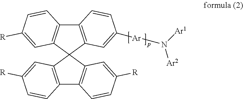
where the symbols and indices used have the meanings given above.

where the symbols and indices used have the meanings given above, and the radicals R on the spirobifluorene preferably stand for H.

where the symbols used have the meanings given above.

where the symbols used have the meanings given above.


where the symbols used have the meanings given above, and the dashed bond indicates the position of the bond from the group to the nitrogen.


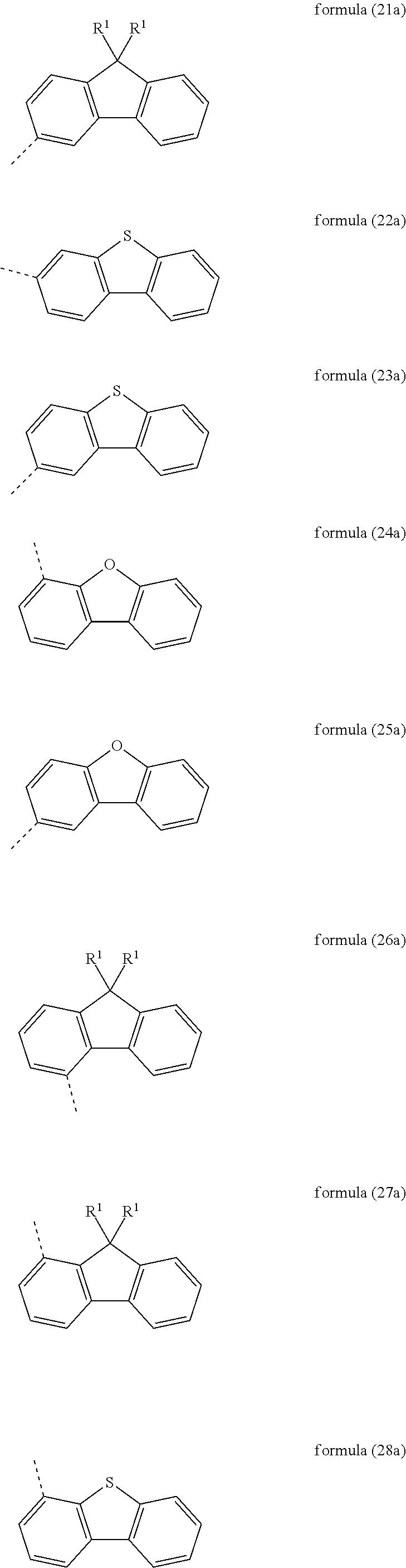
where the symbols used have the meanings given above, and the dashed bond indicates the position of the bond from the group to the nitrogen.
| Ar1 | Ar2 | |
| formula (5) | formula (5) | |
| formula (5) | formula (6) | |
| formula (5) | formula (7) | |
| formula (5) | formula (8) | |
| formula (5) | formula (9) | |
| formula (5) | formula (10) | |
| formula (5) | formula (11) | |
| formula (5) | formula (12) | |
| formula (5) | formula (13) | |
| formula (5) | formula (21) | |
| formula (5) | formula (22) | |
| formula (5) | formula (23) | |
| formula (5) | formula (24) | |
| formula (5) | formula (25) | |
| formula (6) | formula (6) | |
| formula (6) | formula (7) | |
| formula (6) | formula (8) | |
| formula (6) | formula (9) | |
| formula (6) | formula (10) | |
| formula (6) | formula (11) | |
| formula (6) | formula (12) | |
| formula (6) | formula (13) | |
| formula (6) | formula (21) | |
| formula (6) | formula (22) | |
| formula (6) | formula (23) | |
| formula (6) | formula (24) | |
| formula (6) | formula (25) | |
| formula (7) | formula (7) | |
| formula (7) | formula (8) | |
| formula (7) | formula (9) | |
| formula (7) | formula (10) | |
| formula (7) | formula (11) | |
| formula (7) | formula (12) | |
| formula (7) | formula (13) | |
| formula (7) | formula (21) | |
| formula (7) | formula (22) | |
| formula (7) | formula (23) | |
| formula (7) | formula (24) | |
| formula (7) | formula (25) | |
| formula (8) | formula (8) | |
| formula (8) | formula (9) | |
| formula (8) | formula (10) | |
| formula (8) | formula (11) | |
| formula (8) | formula (12) | |
| formula (8) | formula (13) | |
| formula (8) | formula (21) | |
| formula (8) | formula (22) | |
| formula (8) | formula (23) | |
| formula (8) | formula (24) | |
| formula (8) | formula (25) | |
| formula (9) | formula (9) | |
| formula (9) | formula (10) | |
| formula (9) | formula (11) | |
| formula (9) | formula (12) | |
| formula (9) | formula (13) | |
| formula (9) | formula (21) | |
| formula (9) | formula (22) | |
| formula (9) | formula (23) | |
| formula (9) | formula (24) | |
| formula (9) | formula (25) | |
| formula (10) | formula (10) | |
| formula (10) | formula (11) | |
| formula (10) | formula (12) | |
| formula (10) | formula (13) | |
| formula (10) | formula (21) | |
| formula (10) | formula (22) | |
| formula (10) | formula (23) | |
| formula (10) | formula (24) | |
| formula (10) | formula (25) | |
| formula (11) | formula (11) | |
| formula (11) | formula (12) | |
| formula (11) | formula (13) | |
| formula (11) | formula (21) | |
| formula (11) | formula (22) | |
| formula (11) | formula (23) | |
| formula (11) | formula (24) | |
| formula (11) | formula (25) | |
| formula (12) | formula (12) | |
| formula (12) | formula (13) | |
| formula (12) | formula (21) | |
| formula (12) | formula (22) | |
| formula (12) | formula (23) | |
| formula (12) | formula (24) | |
| formula (12) | formula (25) | |
| formula (13) | formula (13) | |
| formula (13) | formula (21) | |
| formula (13) | formula (22) | |
| formula (13) | formula (23) | |
| formula (13) | formula (24) | |
| formula (13) | formula (25) | |
| Ar1 | Ar2 | |
| formula (6) | formula (14) | |
| formula (6) | formula (15) | |
| formula (6) | formula (16) | |
| formula (6) | formula (17) | |
| formula (6) | formula (18) | |
| formula (6) | formula (19) | |
| formula (6) | formula (20) | |
| formula (6) | formula (26) | |
| formula (6) | formula (27) | |
| formula (6) | formula (28) | |
| formula (9) | formula (14) | |
| formula (9) | formula (15) | |
| formula (9) | formula (16) | |
| formula (9) | formula (17) | |
| formula (9) | formula (18) | |
| formula (9) | formula (19) | |
| formula (9) | formula (20) | |
| formula (9) | formula (26) | |
| formula (9) | formula (27) | |
| formula (9) | formula (28) | |

where the symbols used have the meanings given above, and the dashed bond indicates the bond to the spirobifluorene or to Ar.

where the symbols used have the meanings given above, and the dashed bond indicates the bond to the spirobifluorene or to Ar.

where the symbols used have the meanings given above, and the dashed bond indicates the bond to the spirobifluorene.

where the symbols used have the meanings given above, and the dashed bond indicates the bond to the spirobifluorene.


where the symbols used have the meanings given above, and one dashed bond indicates the bond to the spirobifluorene and the other dashed bond indicates the bond to the nitrogen atom.


where the symbols used have the meanings given above, and one dashed bond indicates the bond to the spirobifluorene and the other dashed bond indicates the bond to the nitrogen atom.
- Ar is, identically or differently on each occurrence, an aromatic ring system, where, for p=1 or 2, —(Ar)p— is selected from the groups of the formulae (37) to (50); Ar here may also be connected to Ar1 and/or Ar2 by a group E;
- Ar1, Ar2 are, identically or differently on each occurrence, an aromatic ring system selected from the groups of the formulae (5) to (28); or —NAr1Ar2 stands for a group of one of the formulae (29) to (32); or —Ar—NAr1Ar2 stands for a group of one of the formulae (33) to (36);
- E is on each occurrence, identically or differently, C(R1)2, N(R1), O or S;
- R is selected on each occurrence, identically or differently, from the group consisting of H, D, F, Si(R2)3, a straight-chain alkyl or alkoxy group having 1 to 10 C atoms or a branched or cyclic alkyl or alkoxy group having 3 to 10 C atoms, each of which may be substituted by one or more radicals R2, where one or more non-adjacent CH2 groups may be replaced by O and where one or more H atoms may be replaced by D or F, an aromatic ring system having 6 to 60 C atoms selected from the group consisting of benzene, naphthalene, phenanthrene, fluorene, spirobifluorene or a combination of two or three of these groups, which may in each case be identical or different, which may in each case be substituted by one or more radicals R2, where two or more adjacent substituents R may optionally form a mono- or polycyclic, aliphatic ring system, which may be substituted by one or more radicals R2;
- R1 is, if the radical R1 is bonded to Ar1 or Ar2, selected, identically or differently on each occurrence, from the group consisting of H, D, a straight-chain alkyl group having 1 to 10 C atoms or a branched or cyclic alkyl group having 3 to 10 C atoms;
- or R1 which is bonded to the carbon bridge in formula (29) or (33) is selected, identically or differently on each occurrence, from the group consisting of a straight-chain alkyl group having 1 to 10 C atoms, a branched or cyclic alkyl group having 3 to 10 C atoms or an aromatic ring system having 6 to 30 C atoms, which may be substituted by one or more radicals R2; the two radicals R1 here may also form an aliphatic or aromatic ring system with one another;
- or R1 which is bonded to the nitrogen bridge in formula (32) or (36) is selected from the group consisting of a straight-chain alkyl group having 1 to 10 C atoms, a branched or cyclic alkyl group having 3 to 10 C atoms or an aromatic ring system having 6 to 30 C atoms, which may be substituted by one or more radicals R2;
- R2 is selected on each occurrence, identically or differently, from the group consisting of H, D, a straight-chain alkyl group having 1 to 5 C atoms or a branched or cyclic alkyl group having 3 to 5 C atoms, or an aromatic ring system having 6 to 18 C atoms;
- R3 is selected from the group consisting of H, D, F, an aliphatic hydrocarbon radical having 1 to 10 C atoms, an aromatic ring system having 6 to 24 C atoms, in which one or more H atoms may be replaced by D or F, where two or more adjacent substituents R3 may form a mono- or polycyclic, aliphatic, aromatic or heteroaromatic ring system with one another;
- m is 0, 1 or 2;
- n is on each occurrence, identically or differently, 0, 1 or 2;
- p is 0, 1 or 2.
- Ar is, identically or differently on each occurrence, an aromatic ring system, where, for p=1 or 2, —(Ar)p— is selected from the groups of the formulae (37a) to (50a); Ar here may also be connected to Ar1 or Ar2 by a group E;
- Ar1, Ar2 are, identically or differently on each occurrence, an aromatic ring system selected from the groups of the formulae (5a) to (28a), where at least one group Ar1 and/or Ar2 represents an unbridged group;
- or —NAr1Ar2 stands for a group of one of the formulae (29a) to (32a);
- or —Ar—NAr1Ar2 stands for a group of one of the formulae (33a) to (36a);
- E is on each occurrence, identically or differently, C(R1)2, NR1, O or S;
- R is selected on each occurrence, identically or differently, from the group consisting of H, D, a straight-chain alkyl group having 1 to 10 C atoms or a branched or cyclic alkyl group having 3 to 10 C atoms, each of which may be substituted by one or more radicals R2, an aromatic ring system having 6 to 60 C atoms selected from the group consisting of benzene, naphthalene, phenanthrene, fluorene, spirobifluorene or a combination of two of these groups, which may in each case be identical or different, which may in each case be substituted by one or more radicals R2, where two or more adjacent substituents R may optionally form a mono- or polycyclic, aliphatic ring system, which may be substituted by one or more radicals R2; R is preferably equal to H;
- R1 is, if the radical R1 is bonded to Ar1 or Ar2, selected, identically or differently on each occurrence, from the group consisting of H, D, a straight-chain alkyl group having 1 to 5 C atoms or a branched or cyclic alkyl group having 3 to 5 C atoms;
- or R1 which is bonded to the carbon bridge in formula (29) or (33) is selected, identically or differently on each occurrence, from the group consisting of a straight-chain alkyl group having 1 to 10 C atoms, a branched or cyclic alkyl group having 3 to 10 C atoms or an aromatic ring system having 6 to 30 C atoms, which may be substituted by one or more radicals R2; the two radicals R1 here may also form an aliphatic or aromatic ring system with one another;
- or R1 which is bonded to the nitrogen bridge in formula (32) or (36) is selected from the group consisting of a straight-chain alkyl group having 1 to 10 C atoms, a branched or cyclic alkyl group having 3 to 10 C atoms or an aromatic ring system having 6 to 24 C atoms, which may be substituted by one or more radicals R2;
- R2 is selected on each occurrence, identically or differently, from the group consisting of H, D, a straight-chain alkyl group having 1 to 5 C atoms or a branched or cyclic alkyl group having 3 to 5 C atoms, or an aromatic ring system having 6 to 18 C atoms;
- R3 is selected from the group consisting of H, D, F, an aliphatic hydrocarbon radical having 1 to 5 C atoms, an aromatic ring system having 6 to 12 C atoms, in which one or more H atoms may be replaced by D or F, where two or more adjacent substituents R3 may form a mono- or polycyclic, aliphatic, aromatic or heteroaromatic ring system with one another;
- m is 0;
- n is on each occurrence, identically or differently, 0 or 1;
- p is 0, 1 or 2.
 |
(1) |
 |
(2) |
 |
(3) |
 |
(4) |
 |
(5) |
 |
(6) |
 |
(7) |
 |
(8) |
 |
(9) |
 |
(10) |
 |
(11) |
 |
(12) |
 |
(13) |
 |
(14) |
 |
(15) |
 |
(16) |
 |
(17) |
 |
(18) |
 |
(19) |
 |
(20) |
 |
(21) |
 |
(22) |
 |
(23) |
 |
(24) |
 |
(25) |
 |
(26) |
 |
(27) |
 |
(28) |
 |
(29) |
 |
(30) |
 |
(31) |
 |
(32) |
 |
(33) |
 |
(34) |
 |
(35) |
 |
(36) |
 |
(37) |
 |
(38) |
 |
(39) |
 |
(40) |
 |
(41) |
 |
(42) |
 |
(43) |
 |
(44) |
 |
(45) |
 |
(46) |
 |
(47) |
 |
(48) |
 |
(49) |
 |
(50) |
 |
(51) |
 |
(52) |
 |
(53) |
 |
(54) |
 |
(55) |
 |
(56) |
 |
(57) |
 |
(58) |
 |
(59) |
 |
(60) |
 |
(61) |
 |
(62) |
 |
(63) |
 |
(64) |
 |
(65) |
 |
(66) |
 |
(67) |
 |
(68) |
 |
(69) |
 |
(70) |
 |
(71) |
 |
(72) |
 |
(73) |
 |
(74) |
 |
(75) |
 |
(76) |
 |
(77) |
 |
(78) |
 |
(79) |
 |
(80) |
 |
(81) |
 |
(82) |
 |
(83) |
 |
(84) |
 |
(85) |
 |
(86) |
 |
(87) |
 |
(88) |
 |
(89) |
 |
(90) |
 |
(91) |
 |
(92) |
 |
(93) |
 |
(94) |
 |
(95) |
 |
(96) |
 |
(97) |
 |
(98) |
 |
(99) |
 |
(100) |
 |
(101) |
 |
(102) |
 |
(103) |
 |
(104) |
 |
(105) |
 |
(106) |
 |
(107) |
 |
(108) |
 |
(109) |
 |
(110) |
 |
(111) |
 |
(112) |
 |
(113) |
 |
(114) |
 |
(115) |
 |
(116) |
 |
(117) |
 |
(118) |
 |
(119) |
 |
(120) |
 |
(121) |
 |
(122) |
 |
(123) |
 |
(124) |
 |
(125) |
 |
(126) |
 |
(127) |
 |
(128) |
 |
(129) |
 |
(130) |
 |
(131) |
 |
(132) |
 |
(133) |
 |
(134) |
 |
(135) |
 |
(136) |
 |
(137) |
 |
(138) |
 |
(139) |
 |
(140) |
 |
(141) |
 |
(142) |
 |
(143) |
 |
(144) |
 |
(145) |
 |
(146) |
 |
(147) |
 |
(148) |
 |
(149) |
 |
(150) |
 |
(151) |
 |
(152) |
 |
(153) |
 |
(154) |
 |
(155) |
 |
(156) |
 |
(157) |
 |
(158) |
 |
(159) |
 |
(160) |
 |
(161) |
 |
(162) |
 |
(163) |
 |
(164) |
 |
(165) |
 |
(166) |
 |
(167) |
 |
(168) |
 |
(169) |
 |
(170) |
 |
(171) |
 |
(172) |
 |
(173) |
 |
(174) |
 |
(175) |
 |
(176) |
 |
(177) |
 |
(178) |
 |
(179) |
 |
(180) |
 |
(181) |
 |
(182) |
 |
(183) |
 |
(184) |
 |
(185) |
 |
(186) |
 |
(187) |
 |
(188) |
 |
(189) |
 |
(190) |
 |
(191) |
 |
(192) |
 |
(193) |
 |
(194) |
 |
(195) |
 |
(196) |
 |
(197) |
 |
(198) |
 |
(199) |
 |
(200) |
 |
(201) |
 |
(202) |

- a) a primary amine, followed by coupling to a further aromatic group which is substituted by a reactive leaving group, or
- b) to a secondary amine, or
- c) to a triarylamine derivative.
- 1. The compounds according to the invention are very highly suitable for use in a hole-transport or hole-injection layer in an organic electroluminescent device. They are also suitable, in particular, for use in a layer which is directly adjacent to a phosphorescent emitting layer, since the compounds according to the invention do not extinguish the luminescence.
- 2. The compounds according to the invention, employed as matrix material for fluorescent or phosphorescent emitters, result in very high efficiencies and long lifetimes. This applies, in particular, if the compounds are employed as matrix material together with a further matrix material and a phosphorescent emitter.
- 3. The compounds according to the invention, employed in organic electroluminescent devices, result in high efficiencies and in steep current/voltage curves with low use and operating voltages.
- 4. The compounds according to the invention have high thermal stability and can be sublimed without decomposition and without a residue.
- 5. The compounds according to the invention have high oxidation stability, which has, in particular, a positive effect on the handling of these compounds and on the storage stability for solutions.

| Starting | Starting | |||
| Ex. | material 1 | material 2 | Product | Yield |
| A2 |
 |
 |
 |
90% |
| A3 |
 |
 |
 |
87% |
| A4 |
 |
 |
 |
68% |
| A5 |
 |
 |
 |
69% |
| A6 |
 |
 |
 |
83% |
| A7 |
 |
 |
 |
89% |
| A8 |
 |
 |
 |
65% |
| A9 |
 |
 |
 |
87% |
| A10 |
 |
 |
 |
74% |
| A11 |  |
 |
 |
77% |

| Starting | Starting | |||
| Ex. | material 1 | material 2 | Product | Yield |
| B2 |
 |
 |
 |
70% |
| B3 |
 |
|
 |
72% |
| B4 |
 |
 |
 |
79% |
| B5 |
 |
 |
 |
77% |
| B6 |
 |
 |
 |
68% |
| B7 |
 |
 |
 |
68% |
| B8 |
 |
 |
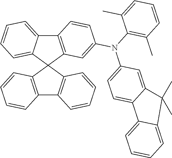 |
68% |
| B9 |
 |
|
 |
63% |
| B10 |
 |
 |
 |
64% |
| B11 |
 |
 |
 |
65% |
| B12 |
 |
 |
 |
89% |
| B13 |
 |
 |
 |
65% |
| B14 |
 |
 |
 |
69% |
| B15 |
 |
 |
 |
65% |
| B16 |
 |
 |
 |
77% |
| B17 comp. |
 |
 |
 |
77% |
| B18 |
 |
 |
 |
65% |
| B19 |  |
 |
 |
65% |
| B20 |
 |
 |
 |
59% |
| B21 |  |
 |
 |
61% |
| B22 |
 |
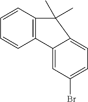 |
 |
78% |
| B23 |
 |
 |
 |
77% |
| B24 |
 |
 |
 |
64% |
| B25 |
 |
 |
 |
69% |
| B26 |
 |
 |
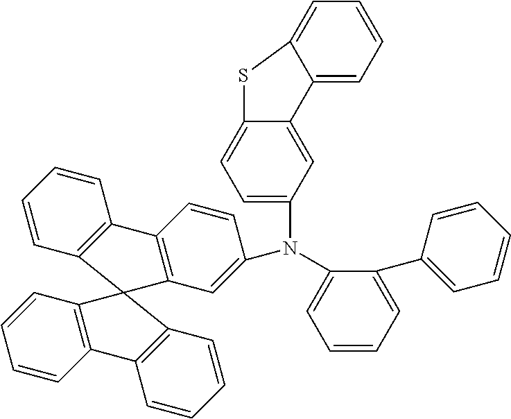 |
66% |
| B27 |
 |
 |
 |
75% |

| Starting | Starting | ||||
| Ex. | material 1 | material 2 | Product | Yield | |
| C1 |  |
 |
 |
 |
73% |
| C2 |  |
 |
 |
 |
75% |
| C3 |  |
 |
 |
 |
79% |
| C4 |  |
 |
 |
 |
78% |
| C5 |  |
 |
 |
 |
65% |
| C6 |  |
 |
 |
 |
70% |
| C7 |  |
 |
 |
 |
80% |

| TABLE 1 |
| Structure of the OLEDs |
| HIL | HTL | IL1 | IL2 | EBL | EML | HBL | ETL | EIL | |
| thick- | thick- | thick- | thick- | thick- | thick- | thick- | thick- | thick- | |
| Ex. | ness | ness | ness | ness | ness | ness | ness | ness | ness |
| C1 | HATCN | SpA1 | — | — | NPB | M1:D1 | — | Alq3 | LiF |
| 5 nm | 140 nm | 20 nm | (95%:5%) | 20 nm | 1 nm | ||||
| 30 nm | |||||||||
| C2 | HATCN | SpA1 | — | — | NPB | M1:D1 | — | ETM1:LiQ | — |
| 5 nm | 140 nm | 20 nm | (95%:5%) | (50%:50%) | |||||
| 30 nm | 20 nm | ||||||||
| C3 | HATCN | SpA1 | — | — | NPB | M2:D2 | — | Alq3 | LiF |
| 5 nm | 110 nm | 20 nm | (90%:10%) | 20 nm | 1 nm | ||||
| 30 nm | |||||||||
| C4 | HATCN | SpNPB | — | — | NPB | M2:D3 | — | ST2:LiQ | — |
| 5 nm | 40 nm | 20 nm | (98.5%:1.5%) | (50%:50%) | |||||
| 30 nm | 20 nm | ||||||||
| C5 | — | SpA1 | HATCN | — | BPA1 | Ket1:TEG1 | — | ST1:LiQ | — |
| 70 nm | 5 nm | 90 nm | (90%:10%) | (50%:50%) | |||||
| 30 nm | 40 nm | ||||||||
| C6 | — | SpA1 | — | — | NPB | Ket1:TSpA1:TER1 | Ket1 | Alq3 | LiF |
| 20 nm | 20 nm | (65%:25%:10%) | 10 nm | 20 nm | 1 nm | ||||
| 30 nm | |||||||||
| C7 | — | SpA1 | HATCN | — | BPA1 | ST1:CBP:TEG1 | ST1 | ST1:LiQ | — |
| 70 nm | 5 nm | 90 nm | (30%:60%:10%) | 10 nm | (50%:50%) | ||||
| 30 nm | 30 nm | ||||||||
| C8 | — | SpA1 | HATCN | — | BPA1 | ST1:TCTA:TEG1 | — | ST1:LiQ | — |
| 70 nm | 5 nm | 90 nm | (30%:60%:10%) | (50%:50%) | |||||
| 30 nm | 30 nm | ||||||||
| C9 | HATCN | — | — | — | BPA1 | Ket1:FTPh:TEG1 | Ket1 | ETM2 | LiF |
| 20 nm | 20 nm | (60%:30%:10%) | 10 nm | 20 nm | 1 nm | ||||
| 30 nm | |||||||||
| C10 | HATCN | — | — | — | BPA1 | Ket1:TCTA:TEG1 | Ket1 | ETM2 | LiF |
| 20 nm | 20 nm | (60%:30%:10%) | 10 nm | 20 nm | 1 nm | ||||
| 30 nm | |||||||||
| C11 | HATCN | — | — | — | BPA1 | Ket1:CBP:TEG1 | Ket1 | ETM2 | LiF |
| 20 nm | 20 nm | (60%:30%:10%) | 10 nm | 20 nm | 1 nm | ||||
| 30 nm | |||||||||
| C12 | — | SpA1 | HATCN | — | BPA1 | DAP1:CBP:TEG1 | — | ST1:LiQ | — |
| 70 nm | 5 nm | 90 nm | (30%:60%:10%) | (50%:50%) | |||||
| 30 nm | 30 nm | ||||||||
| C13 | — | SpA1 | HATCN | — | BPA1 | IC1:TEG1 | ST1 | ST1:LiQ | — |
| 70 nm | 5 nm | 90 nm | (90%:10%) | 10 nm | (50%:50%) | ||||
| 30 nm | 30 nm | ||||||||
| C14 | HATCN | SpA1 | HATCN | — | BPA1 | M2:D4 | — | ST1:LiQ | LiQ |
| 5 nm | 140 nm | 5 nm | 20 nm | (95%:5%) | (50%:50%) | 1 nm | |||
| 20 nm | 30 nm | ||||||||
| C15 | HATCN | SpA1 | HATCN | — | NPB | M2:D4 | — | ST1:LiQ | LiQ |
| 5 nm | 140 nm | 5 nm | 20 nm | (95%:5%) | (50%:50%) | 1 nm | |||
| 20 nm | 30 nm | ||||||||
| C16 | HATCN | TIFA1 | HATCN | — | CbzA1 | M2:D4 | — | ST2:LiQ | LiQ |
| 5 nm | 140 nm | 5 nm | 20 nm | (95%:5%) | (50%:50%) | 1 nm | |||
| 20 nm | 30 nm | ||||||||
| C17 | HATCN | SpA1 | HATCN | — | CbzA1 | IC1:TEG1 | — | ST2:LiQ | LiQ |
| 5 nm | 140 nm | 5 nm | 20 nm | (90%:10%) | (50%:50%) | 1 nm | |||
| 30 nm | 40 nm | ||||||||
| C18 | HATCN | SpA1 | HATCN | CbzA1 | CbzA1 | M2:D4 | — | ST2:LiQ | LiQ |
| 5 nm | 140 nm | 5 nm | 10 nm | 20 nm | (95%:5%) | (50%:50%) | 1 nm | ||
| 20 nm | 30 nm | ||||||||
| C19 | HATCN | SpA1 | HATCN | — | SpA-tb | IC1:TEG1 | — | ST2:LiQ | LiQ |
| 5 nm | 130 nm | 5 nm | 20 nm | (90%:10%) | (50%:50%) | 1 nm | |||
| 30 nm | 40 nm | ||||||||
| C20 | HATCN | SpA1 | HATCN | — | SpA-tb | IC1:TEG1 | — | ST2:LiQ | LiQ |
| 5 nm | 80 nm | 5 nm | 70 nm | (90%:10%) | (50%:50%) | 1 nm | |||
| 30 nm | 40 nm | ||||||||
| I1 | — | SpA1 | HATCN | — | B1 | IC1:TEG1 | ST1 | ST1:LiQ | — |
| 70 nm | 5 nm | 90 nm | (90%:10%) | 10 nm | (50%:50%) | ||||
| 30 nm | 30 nm | ||||||||
| I2 | — | SpA1 | — | — | NPB | Ket1:B1:TER1 | Ket1 | Alq3 | LiF |
| 20 nm | 20 nm | (65%:25%:10%) | 10 nm | 20 nm | 1 nm | ||||
| 30 nm | |||||||||
| I3 | HATCN | SpNPB | — | — | B2 | M2:D3 | — | ST2:LiQ | — |
| 5 nm | 40 nm | 20 nm | (98.5%:1.5%) | (50%:50%) | |||||
| 30 nm | 20 nm | ||||||||
| I4 | — | SpA1 | HATCN | — | BPA1 | ST1:B2:TEG1 | ST1 | ST1:LiQ | — |
| 70 nm | 5 nm | 90 nm | (30%:60%:10%) | 10 nm | (50%:50%) | ||||
| 30 nm | 30 nm | ||||||||
| I5 | HATCN | — | — | — | BPA1 | Ket1:B2:TEG1 | Ket1 | ETM2 | LiF |
| 20 nm | 20 nm | (60%:30%:10%) | 10 nm | 20 nm | 1 nm | ||||
| 30 nm | |||||||||
| I6 | HATCN | SpA1 | — | — | B3 | M1:D1 | — | ETM1:LiQ | — |
| 5 nm | 140 nm | 20 nm | (95%:5%) | (50%:50%) | |||||
| 30 nm | 20 nm | ||||||||
| I7 | HATCN | SpA1 | — | — | B4 | M2:D2 | — | Alq3 | LiF |
| 5 nm | 110 nm | 20 nm | (90%:10%) | 20 nm | 1 nm | ||||
| 30 nm | |||||||||
| I8 | HATCN | SpA1 | — | — | B5 | M2:D2 | — | Alq3 | LiF |
| 5 nm | 110 nm | 20 nm | (90%:10%) | 20 nm | 1 nm | ||||
| 30 nm | |||||||||
| I9 | HATCN | SpA1 | — | — | B6 | M2:D2 | — | Alq3 | LiF |
| 5 nm | 110 nm | 20 nm | (90%:10%) | 20 nm | 1 nm | ||||
| 30 nm | |||||||||
| I10 | HATCN | SpA1 | — | — | B7 | M2:D2 | — | Alq3 | LiF |
| 5 nm | 110 nm | 20 nm | (90%:10%) | 20 nm | 1 nm | ||||
| 30 nm | |||||||||
| I11 | HATCN | SpA1 | — | — | B8 | M1:D1 | — | ETM1:LiQ | — |
| 5 nm | 140 nm | 20 nm | (95%:5%) | (50%:50%) | |||||
| 30 nm | 20 nm | ||||||||
| I12 | — | SpA1 | HATCN | — | B8 | IC1:TEG1 | ST1 | ST1:LiQ | — |
| 70 nm | 5 nm | 90 nm | (90%:10%) | 10 nm | (50%:50%) | ||||
| 30 nm | 30 nm | ||||||||
| I13 | — | SpA1 | HATCN | — | BPA1 | ST1:B9:TEG1 | ST1 | ST1:LiQ | — |
| 70 nm | 5 nm | 90 nm | (30%:60%:10%) | 10 nm | (50%:50%) | ||||
| 30 nm | 30 nm | ||||||||
| I14 | — | SpA1 | HATCN | — | BPA1 | DAP1:B9:TEG1 | — | ST1:LiQ | — |
| 70 nm | 5 nm | 90 nm | (30%:60%:10%) | (50%:50%) | |||||
| 30 nm | 30 nm | ||||||||
| I15 | HATCN | SpA1 | — | — | B10 | M1:D1 | — | ETM1:LiQ | — |
| 5 nm | 140 nm | 20 nm | (95%:5%) | (50%:50%) | |||||
| 30 nm | 20 nm | ||||||||
| I16 | — | SpA1 | HATCN | — | B10 | Ket1:TEG1 | — | ST1:LiQ | — |
| 70 nm | 5 nm | 90 nm | (90%:10%) | (50%:50%) | |||||
| 30 nm | 40 nm | ||||||||
| I17 | HATCN | SpA1 | — | — | B11 | M1:D1 | — | Alq3 | LiF |
| 5 nm | 140 nm | 20 nm | (95%:5%) | 20 nm | 1 nm | ||||
| 30 nm | |||||||||
| I18 | HATCN | SpA1 | — | — | B11 | M2:D2 | — | Alq3 | LiF |
| 5 nm | 110 nm | 20 nm | (90%:10%) | 20 nm | 1 nm | ||||
| 30 nm | |||||||||
| I19 | — | SpA1 | HATCN | — | B11 | IC1:TEG1 | ST1 | ST1:LiQ | — |
| 70 nm | 5 nm | 90 nm | (90%:10%) | 10 nm | (50%:50%) | ||||
| 30 nm | 30 nm | ||||||||
| I20 | HATCN | SpNPB | — | — | B12 | M2:D3 | — | ST2:LiQ | — |
| 5 nm | 40 nm | 20 nm | (98.5%:1.5%) | (50%:50%) | |||||
| 30 nm | 20 nm | ||||||||
| I21 | — | SpA1 | HATCN | — | BPA1 | ST1:B12:TEG1 | ST1 | ST1:LiQ | — |
| 70 nm | 5 nm | 90 nm | (30%:60%:10%) | 10 nm | (50%:50%) | ||||
| 30 nm | 30 nm | ||||||||
| I22 | HATCN | SpNPB | — | — | B13 | M2:D3 | — | ST2:LiQ | — |
| 5 nm | 40 nm | 20 nm | (98.5%:1.5%) | (50%:50%) | |||||
| 30 nm | 20 nm | ||||||||
| I23 | — | SpA1 | HATCN | — | BPA1 | ST1:B13:TEG1 | ST1 | ST1:LiQ | — |
| 70 nm | 5 nm | 90 nm | (30%:60%:10%) | 10 nm | (50%:50%) | ||||
| 30 nm | 30 nm | ||||||||
| I24 | HATCN | SpA1 | — | — | B14 | M1:D1 | — | Alq3 | LiF |
| 5 nm | 140 nm | 20 nm | (95%:5%) | 20 nm | 1 nm | ||||
| 30 nm | |||||||||
| I25 | HATCN | SpA1 | — | — | B14 | M2:D2 | — | Alq3 | LiF |
| 5 nm | 110 nm | 20 nm | (90%:10%) | 20 nm | 1 nm | ||||
| 30 nm | |||||||||
| I26 | HATCN | SpA1 | — | — | B15 | M1:D1 | — | Alq3 | LiF |
| 5 nm | 140 nm | 20 nm | (95%:5%) | 20 nm | 1 nm | ||||
| 30 nm | |||||||||
| I27 | HATCN | SpA1 | — | — | B15 | M1:D1 | — | ETM1:LiQ | — |
| 5 nm | 140 nm | 20 nm | (95%:5%) | (50%:50%) | |||||
| 30 nm | 20 nm | ||||||||
| I28 | HATCN | SpA1 | — | — | B16 | M1:D1 | — | ETM1:LiQ | — |
| 5 nm | 140 nm | 20 nm | (95%:5%) | (50%:50%) | |||||
| 30 nm | 20 nm | ||||||||
| I29 | HATCN | SpA1 | — | — | B17 | M1:D1 | — | ETM1:LiQ | — |
| 5 nm | 140 nm | 20 nm | (95%:5%) | (50%:50%) | |||||
| 30 nm | 20 nm | ||||||||
| I30 | HATCN | SpA1 | — | — | B18 | M1:D1 | — | ETM1:LiQ | — |
| 5 nm | 140 nm | 20 nm | (95%:5%) | (50%:50%) | |||||
| 30 nm | 20 nm | ||||||||
| I31 | HATCN | SpNPB | — | — | B18 | M2:D3 | — | ST2:LiQ | — |
| 5 nm | 40 nm | 20 nm | (98.5%:1.5%) | (50%:50%) | |||||
| 30 nm | 20 nm | ||||||||
| I32 | — | SpA1 | — | — | NPB | Ket1:B18:TER1 | Ket1 | Alq3 | LiF |
| 20 nm | 20 nm | (65%:25%:10%) | 10 nm | 20 nm | 1 nm | ||||
| 30 nm | |||||||||
| I33 | — | SpA1 | HATCN | — | B19 | IC1:TEG1 | ST1 | ST1:LiQ | — |
| 70 nm | 5 nm | 90 nm | (90%:10%) | 10 nm | (50%:50%) | ||||
| 30 nm | 30 nm | ||||||||
| I34 | — | SpA1 | HATCN | — | B20 | IC1:TEG1 | ST1 | ST1:LiQ | — |
| 70 nm | 5 nm | 90 nm | (90%:10%) | 10 nm | (50%:50%) | ||||
| 30 nm | 30 nm | ||||||||
| I35 | — | SpA1 | HATCN | — | B21 | IC1:TEG1 | ST1 | ST1:LiQ | — |
| 70 nm | 5 nm | 90 nm | (90%:10%) | 10 nm | (50%:50%) | ||||
| 30 nm | 30 nm | ||||||||
| I36 | HATCN | SpA1 | — | — | C | M1:D1 | — | Alq3 | LiF |
| 5 nm | 140 nm | 20 nm | (95%:5%) | 20 nm | 1 nm | ||||
| 30 nm | |||||||||
| I37 | HATCN | SpA1 | — | — | C | M1:D1 | — | ETM1:LiQ | — |
| 5 nm | 140 nm | 20 nm | (95%:5%) | (50%:50%) | |||||
| 30 nm | 20 nm | ||||||||
| I38 | HATCN | SpA1 | — | — | C | M2:D2 | — | Alq3 | LiF |
| 5 nm | 110 nm | 20 nm | (90%:10%) | 20 nm | 1 nm | ||||
| 30 nm | |||||||||
| I39 | — | SpA1 | HATCN | — | C | IC1:TEG1 | ST1 | ST1:LiQ | — |
| 70 nm | 5 nm | 90 nm | (90%:10%) | 10 nm | (50%:50%) | ||||
| 30 nm | 30 nm | ||||||||
| I40 | HATCN | SpA1 | HATCN | — | C | M2:D4 | — | ST2:LiQ | LiQ |
| 5 nm | 140 nm | 5 nm | 20 nm | (95%:5%) | (50%:50%) | 1 nm | |||
| 20 nm | 30 nm | ||||||||
| I41 | HATCN | SpA1 | HATCN | — | C | M2:D4 | — | ST1:LiQ | LiQ |
| 5 nm | 140 nm | 5 nm | 20 nm | (95%:5%) | (50%:50%) | 1 nm | |||
| 20 nm | 30 nm | ||||||||
| I42 | HATCN | TIFA1 | HATCN | — | B1 | M2:D4 | — | ST2:LiQ | LiQ |
| 5 nm | 140 nm | 5 nm | 20 nm | (95%:5%) | (50%:50%) | 1 nm | |||
| 20 nm | 30 nm | ||||||||
| I43 | HATCN | TIFA1 | HATCN | — | C | M2:D4 | — | ST2:LiQ | LiQ |
| 5 nm | 140 nm | 5 nm | 20 nm | (95%:5%) | (50%:50%) | 1 nm | |||
| 20 nm | 30 nm | ||||||||
| I44 | HATCN | SpA1 | HATCN | C | B18 | M2:D4 | — | ST2:LiQ | LiQ |
| 5 nm | 125 nm | 5 nm | 10 nm | 20 nm | (95%:5%) | (50%:50%) | 1 nm | ||
| 20 nm | 30 nm | ||||||||
| I45 | HATCN | SpA1 | HATCN | C | D | M2:D4 | — | ST2:LiQ | LiQ |
| 5 nm | 125 nm | 5 nm | 10 nm | 20 nm | (95%:5%) | (50%:50%) | 1 nm | ||
| 20 nm | 30 nm | ||||||||
| I46 | HATCN | SpA1 | HATCN | C | B19 | M2:D4 | — | ST2:LiQ | LiQ |
| 5 nm | 125 nm | 5 nm | 10 nm | 20 nm | (95%:5%) | (50%:50%) | 1 nm | ||
| 20 nm | 30 nm | ||||||||
| I47 | HATCN | SpA1 | HATCN | — | C5 | M2:D4 | — | ST2:LiQ | LiQ |
| 5 nm | 140 nm | 5 nm | 20 nm | (95%:5%) | (50%:50%) | 1 nm | |||
| 20 nm | 30 nm | ||||||||
| I48 | HATCN | SpA1 | HATCN | CbzA1 | C6 | M2:D4 | — | ST2:LiQ | LiQ |
| 5 nm | 140 nm | 5 nm | 10 nm | 20 nm | (95%:5%) | (50%:50%) | 1 nm | ||
| 20 nm | 30 nm | ||||||||
| I49 | HATCN | SpA1 | HATCN | — | C6 | IC1:TEG1 | — | ST2:LiQ | LiQ |
| 5 nm | 140 nm | 5 nm | 20 nm | (90%:10%) | (50%:50%) | 1 nm | |||
| 30 nm | 40 nm | ||||||||
| I50 | HATCN | SpA1 | HATCN | — | C7 | IC1:TEG1 | — | ST2:LiQ | LiQ |
| 5 nm | 140 nm | 5 nm | 20 nm | (90%:10%) | (50%:50%) | 1 nm | |||
| 30 nm | 40 nm | ||||||||
| I51 | HATCN | SpA1 | HATCN | — | B22 | IC1:TEG1 | — | ST2:LiQ | LiQ |
| 5 nm | 140 nm | 5 nm | 20 nm | (90%:10%) | (50%:50%) | 1 nm | |||
| 30 nm | 40 nm | ||||||||
| I52 | HATCN | TIFA1 | HATCN | — | C1 | M2:D4 | — | ST2:LiQ | LiQ |
| 5 nm | 140 nm | 5 nm | 20 nm | (95%:5%) | (50%:50%) | 1 nm | |||
| 20 nm | 30 nm | ||||||||
| I53 | HATCN | SpA1 | HATCN | — | B23 | IC1:TEG1 | — | ST2:LiQ | LiQ |
| 5 nm | 140 nm | 5 nm | 20 nm | (90%:10%) | (50%:50%) | 1 nm | |||
| 30 nm | 40 nm | ||||||||
| I54 | — | SpA1 | HATCN | — | B24 | IC1:TEG1 | ST1 | ST1:LiQ | — |
| 70 nm | 5 nm | 90 nm | (90%:10%) | 10 nm | (50%:50%) | ||||
| 30 nm | 30 nm | ||||||||
| I55 | HATCN | SpA1 | HATCN | — | B24 | M2:D4 | — | ST2:LiQ | LiQ |
| 5 nm | 140 nm | 5 nm | 20 nm | (95%:5%) | (50%:50%) | 1 nm | |||
| 20 nm | 30 nm | ||||||||
| I56 | HATCN | SpA1 | HATCN | — | B25 | M2:D4 | — | ST2:LiQ | LiQ |
| 5 nm | 140 nm | 5 nm | 20 nm | (95%:5%) | (50%:50%) | 1 nm | |||
| 20 nm | 30 nm | ||||||||
| I57 | — | SpA1 | HATCN | — | C2 | IC1:TEG1 | ST1 | ST1:LiQ | — |
| 70 nm | 5 nm | 90 nm | (90%:10%) | 10 nm | (50%:50%) | ||||
| 30 nm | 30 nm | ||||||||
| I58 | — | SpA1 | HATCN | — | C4 | IC1:TEG1 | ST1 | ST1:LiQ | — |
| 70 nm | 5 nm | 90 nm | (90%:10%) | 10 nm | (50%:50%) | ||||
| 30 nm | 30 nm | ||||||||
| I59 | HATCN | SpA1 | HATCN | CbzA1 | B26 | M2:D4 | — | ST2:LiQ | LiQ |
| 5 nm | 140 nm | 5 nm | 10 nm | 20 nm | (95%:5%) | (50%:50%) | 1 nm | ||
| 20 nm | 30 nm | ||||||||
| I60 | HATCN | SpA1 | HATCN | CbzA1 | B27 | M2:D4 | — | ST2:LiQ | LiQ |
| 5 nm | 140 nm | 5 nm | 10 nm | 20 nm | (95%:5%) | (50%:50%) | 1 nm | ||
| 20 nm | 30 nm | ||||||||
| I61 | HATCN | SpA1 | HATCN | — | C | IC1:TEG1 | — | ST2:LiQ | LiQ |
| 5 nm | 130 nm | 5 nm | 20 nm | (90%:10%) | (50%:50%) | 1 nm | |||
| 30 nm | 40 nm | ||||||||
| I62 | HATCN | SpA1 | HATCN | — | C | IC1:TEG1 | — | ST2:LiQ | LiQ |
| 5 nm | 80 nm | 5 nm | 70 nm | (90%:10%) | (50%:50%) | 1 nm | |||
| 30 nm | 40 nm | ||||||||
| I63 | HATCN | SpA1 | HATCN | — | C5 | IC1:TEG1 | — | ST2:LiQ | LiQ |
| 5 nm | 130 nm | 5 nm | 20 nm | (90%:10%) | (50%:50%) | 1 nm | |||
| 30 nm | 40 nm | ||||||||
| I64 | HATCN | SpA1 | HATCN | — | C5 | IC1:TEG1 | — | ST2:LiQ | LiQ |
| 5 nm | 80 nm | 5 nm | 70 nm | (90%:10%) | (50%:50%) | 1 nm | |||
| 30 nm | 40 nm | ||||||||
| I65 | HATCN | SpA1 | HATCN | — | B16 | IC1:TEG1 | — | ST2:LiQ | LiQ |
| 5 nm | 130 nm | 5 nm | 20 nm | (90%:10%) | (50%:50%) | 1 nm | |||
| 30 nm | 40 nm | ||||||||
| I66 | HATCN | SpA1 | HATCN | — | B16 | IC1:TEG1 | — | ST2:LiQ | LiQ |
| 5 nm | 80 nm | 5 nm | 70 nm | (90%:10%) | (50%:50%) | 1 nm | |||
| 30 nm | 40 nm | ||||||||
| I67 | HATCN | SpA1 | HATCN | — | B18 | M2:D4 | — | ST2:LiQ | LiQ |
| 5 nm | 140 nm | 5 nm | 20 nm | (95%:5%) | (50%:50%) | 1 nm | |||
| 20 nm | 30 nm | ||||||||
| I68 | — | B6 | HATCN | — | BPA1 | IC1:TEG1 | ST1 | ST1:LiQ | — |
| 70 nm | 5 nm | 90 nm | (90%:10%) | 10 nm | (50%:50%) | ||||
| 30 nm | 30 nm | ||||||||
| TABLE 2 |
| Data for the OLEDs |
| U1000 | CE1000 | PE1000 | EQE | CIE x/y at | L0 | L1 | Lifetime | |
| Ex. | (V) | (cd/A) | (lm/W) | 1000 | 1000 cd/m2 | (cd/m2) | % | (h) |
| C1 | 6.4 | 5.1 | 2.5 | 4.2% | 0.14/0.15 | 6000 | 50 | 150 |
| C2 | 4.7 | 8.1 | 5.4 | 6.3% | 0.14/0.16 | 6000 | 50 | 145 |
| C3 | 5.0 | 17 | 11 | 5.0% | 0.28/0.61 | 25000 | 50 | 480 |
| C4 | 4.3 | 9.8 | 7.1 | 7.6% | 0.141/0.160 | 6000 | 50 | 210 |
| C5 | 3.9 | 41 | 33 | 11.0% | 0.36/0.61 | 4000 | 80 | 315 |
| C6 | 4.3 | 7.7 | 5.6 | 10.8% | 0.68/0.32 | 4000 | 80 | 360 |
| C7 | 4.4 | 48 | 34 | 13.3% | 0.37/0.60 | 4000 | 80 | 450 |
| C8 | 4.2 | 43 | 32 | 12.0% | 0.35/0.60 | 4000 | 80 | 195 |
| C9 | 4.0 | 46 | 36 | 12.8% | 0.36/0.61 | 4000 | 80 | 370 |
| C10 | 3.9 | 42 | 34 | 11.6% | 0.35/0.60 | 4000 | 80 | 175 |
| C11 | 4.1 | 44 | 34 | 12.3% | 0.36/0.61 | 4000 | 80 | 280 |
| C12 | 4.6 | 47 | 32 | 13.2% | 0.36/0.60 | 4000 | 80 | 490 |
| C13 | 3.5 | 53 | 48 | 14.8% | 0.36/0.60 | 4000 | 80 | 430 |
| C14 | 4.2 | 7.0 | 9.5 | 7.4% | 0.14/0.16 | 6000 | 50 | 250 |
| C15 | 4.2 | 8.2 | 6.3 | 6.5% | 0.14/0.16 | 6000 | 50 | 315 |
| C16 | 4.4 | 7.6 | 5.4 | 5.4% | 0.14/0.18 | 6000 | 65 | 240 |
| C17 | 3.5 | 59 | 53 | 16.4% | 0.37/0.60 | 10000 | 70 | 235 |
| C18 | 4.3 | 8.4 | 6.1 | 6.5% | 0.14/0.16 | 6000 | 50 | 320 |
| C19 | 3.5 | 59 | 53 | 16.3% | 0.37/0.60 | 10000 | 65 | 310 |
| C20 | 4.1 | 57 | 43 | 15.9% | 0.37/0.60 | 10000 | 65 | 210 |
| I1 | 3.7 | 59 | 50 | 16.4% | 0.36/0.60 | 4000 | 80 | 490 |
| I2 | 4.2 | 9.0 | 6.7 | 12.8% | 0.68/0.32 | 4000 | 80 | 460 |
| I3 | 4.4 | 10.4 | 7.4 | 8.1% | 0.14/0.16 | 6000 | 50 | 260 |
| I4 | 4.0 | 51 | 40 | 14.2% | 0.37/0.61 | 4000 | 80 | 620 |
| I5 | 3.7 | 50 | 43 | 14.0% | 0.37/0.61 | 4000 | 80 | 550 |
| I6 | 4.6 | 9.1 | 6.3 | 7.1% | 0.14/0.16 | 6000 | 50 | 130 |
| I7 | 5.1 | 19 | 12 | 5.4% | 0.28/0.61 | 25000 | 50 | 460 |
| I8 | 5.1 | 18 | 11 | 5.2% | 0.28/0.61 | 25000 | 50 | 520 |
| I9 | 4.8 | 20 | 13 | 5.8% | 0.28/0.61 | 25000 | 50 | 530 |
| I10 | 5.0 | 18 | 11 | 5.3% | 0.28/0.61 | 25000 | 50 | 430 |
| I11 | 4.7 | 8.7 | 5.8 | 6.8% | 0.14/0.15 | 6000 | 50 | 160 |
| I12 | 3.4 | 58 | 54 | 16.1% | 0.36/0.60 | 4000 | 80 | 420 |
| I13 | 4.1 | 50 | 38 | 13.9% | 0.37/0.61 | 4000 | 80 | 470 |
| I14 | 3.9 | 52 | 41 | 14.4% | 0.37/0.61 | 4000 | 80 | 460 |
| I15 | 4.8 | 9.2 | 6.1 | 7.2% | 0.14/0.15 | 6000 | 50 | 230 |
| I16 | 4.0 | 46 | 36 | 12.8% | 0.37/0.60 | 4000 | 80 | 470 |
| I17 | 6.1 | 6.7 | 3.4 | 5.5% | 0.14/0.15 | 6000 | 50 | 230 |
| I18 | 5.2 | 20 | 12 | 5.7% | 0.28/0.61 | 25000 | 50 | 620 |
| I19 | 3.5 | 56 | 50 | 15.6% | 0.36/0.60 | 4000 | 80 | 550 |
| I20 | 4.5 | 11 | 7.6 | 8.4% | 0.14/0.16 | 6000 | 50 | 290 |
| I21 | 3.8 | 47 | 40 | 13.1% | 0.36/0.62 | 4000 | 80 | 440 |
| I22 | 4.5 | 11 | 7.3 | 8.2% | 0.14/0.16 | 6000 | 50 | 270 |
| I23 | 3.7 | 49 | 41 | 13.6% | 0.36/0.62 | 4000 | 80 | 470 |
| I24 | 6.2 | 6.2 | 3.1 | 5.1% | 0.14/0.15 | 6000 | 50 | 175 |
| I25 | 5.0 | 19 | 12 | 5.7% | 0.28/0.61 | 25000 | 50 | 510 |
| I26 | 6.3 | 6.4 | 3.2 | 5.3% | 0.14/0.15 | 6000 | 50 | 190 |
| I27 | 4.8 | 9.5 | 6.2 | 7.4% | 0.14/0.15 | 6000 | 50 | 175 |
| I28 | 4.5 | 8.7 | 6.1 | 6.8% | 0.14/0.15 | 6000 | 50 | 180 |
| I29 | 4.6 | 7.9 | 5.4 | 6.2% | 0.14/0.16 | 6000 | 50 | 165 |
| I30 | 4.8 | 9.5 | 6.3 | 7.4% | 0.14/0.16 | 6000 | 50 | 245 |
| I31 | 4.4 | 11 | 7.5 | 8.2% | 0.14/0.160 | 6000 | 50 | 280 |
| I32 | 4.4 | 8.2 | 5.9 | 11.6% | 0.68/0.32 | 4000 | 80 | 420 |
| I33 | 3.6 | 57 | 50 | 15.9% | 0.36/0.60 | 4000 | 80 | 410 |
| I34 | 3.8 | 58 | 49 | 16.1% | 0.36/0.60 | 4000 | 80 | 380 |
| I35 | 3.4 | 59 | 54 | 16.4% | 0.37/0.60 | 4000 | 80 | 360 |
| I36 | 6.2 | 6.6 | 3.3 | 5.4% | 0.14/0.15 | 6000 | 50 | 215 |
| I37 | 4.7 | 9.5 | 6.3 | 7.4% | 0.14/0.16 | 6000 | 50 | 240 |
| I38 | 5.2 | 19 | 12 | 5.7% | 0.28/0.61 | 25000 | 50 | 610 |
| I39 | 3.6 | 57 | 50 | 15.8% | 0.36/0.60 | 4000 | 80 | 530 |
| I40 | 4.2 | 10 | 7.4 | 7.7% | 0.14/0.16 | 6000 | 50 | 390 |
| I41 | 3.9 | 10.3 | 8.3 | 8.3% | 0.14/0.16 | 6000 | 50 | 360 |
| I42 | 4.5 | 8.3 | 5.7 | 5.9% | 0.14/0.18 | 6000 | 65 | 280 |
| I43 | 4.3 | 9.0 | 6.6 | 6.4% | 0.14/0.18 | 6000 | 65 | 295 |
| I44 | 4.3 | 9.0 | 6.3 | 7.3% | 0.14/0.15 | 6000 | 65 | 185 |
| I45 | 4.5 | 9.5 | 6.7 | 7.5% | 0.14/0.16 | 6000 | 65 | 190 |
| I46 | 4.7 | 10.5 | 6.9 | 8.5% | 0.14/0.16 | 6000 | 65 | 165 |
| I47 | 4.2 | 9.7 | 7.2 | 7.5% | 0.14/0.16 | 6000 | 50 | 395 |
| I48 | 4.3 | 10.1 | 7.7 | 8.4% | 0.14/0.16 | 6000 | 50 | 300 |
| I49 | 3.3 | 62 | 58 | 17.1% | 0.37/0.60 | 10000 | 70 | 230 |
| I50 | 3.4 | 61 | 57 | 17.3% | 0.37/0.60 | 10000 | 70 | 240 |
| I51 | 3.5 | 64 | 58 | 17.7% | 0.37/0.60 | 10000 | 70 | 225 |
| I52 | 4.2 | 9.9 | 7.4 | 7.8% | 0.14/0.16 | 6000 | 50 | 340 |
| I53 | 3.6 | 60 | 53 | 16.5% | 0.37/0.60 | 10000 | 70 | 215 |
| I54 | 3.5 | 56 | 49 | 15.4% | 0.36/0.60 | 4000 | 80 | 495 |
| I55 | 4.3 | 8.7 | 6.5 | 6.8% | 0.14/0.16 | 6000 | 50 | 350 |
| I56 | 4.2 | 9.5 | 7.0 | 7.3% | 0.14/0.16 | 6000 | 50 | 355 |
| I57 | 3.5 | 56 | 50 | 15.4% | 0.36/0.60 | 4000 | 80 | 460 |
| I58 | 3.6 | 59 | 52 | 16.3% | 0.36/0.60 | 4000 | 80 | 490 |
| I59 | 4.2 | 9.9 | 7.4 | 7.7% | 0.14/0.60 | 6000 | 50 | 240 |
| I60 | 4.2 | 9.5 | 7.1 | 7.4% | 0.14/0.60 | 6000 | 50 | 290 |
| I61 | 3.4 | 61 | 56 | 16.8% | 0.37/0.60 | 10000 | 65 | 380 |
| I62 | 3.5 | 60 | 54 | 16.5% | 0.37/0.60 | 10000 | 65 | 370 |
| I63 | 3.5 | 61 | 55 | 16.9% | 0.37/0.60 | 10000 | 65 | 305 |
| I64 | 3.7 | 59 | 50 | 16.3% | 0.37/0.60 | 10000 | 65 | 270 |
| I65 | 3.4 | 56 | 51 | 15.4% | 0.37/0.60 | 10000 | 65 | 340 |
| I66 | 3.6 | 55 | 47 | 15.3% | 0.37/0.60 | 10000 | 65 | 345 |
| I67 | 4.2 | 8.8 | 6.6 | 7.1% | 0.14/0.16 | 6000 | 50 | 315 |
| I68 | 3.4 | 55 | 50 | 15.1% | 0.36/0.60 | 4000 | 80 | 465 |
| Sol1 | 4.8 | 8.4 | 5.5 | 6.9% | 0.14/0.15 | 6000 | 50 | 155 |
| Sol2 | 4.7 | 6.8 | 4.6 | 5.5% | 0.14/0.15 | 6000 | 50 | 260 |
| Sol3 | 4.7 | 6.4 | 4.3 | 5.4% | 0.14/0.14 | 6000 | 65 | 190 |
| TABLE 3 |
| Structural formulae of the materials for the OLEDs |
 |
HATCN |
 |
SpA1 |
 |
NPB (prior art) |
 |
BPA1 (prior art) |
 |
Alq3 |
 |
M1 |
 |
M2 |
 |
D1 |
 |
D2 |
 |
ETM1 |
 |
ST1 |
 |
ETM2 |
 |
LiQ |
 |
TEG1 |
 |
CBP (prior art) |
 |
Ket1 |
 |
TCTA (prior art) |
 |
ST2 |
 |
DAP1 |
 |
FTPh (prior art) |
 |
D3 |
 |
SpNBP |
 |
IC1 |
 |
TSpA1 (prior art) |
 |
TER1 |
 |
D4 |
 |
TIFA1 |
 |
CbzA1 (prior art) |
 |
SpA-tb (prior art) |
Claims (21)


Applications Claiming Priority (4)
| Application Number | Priority Date | Filing Date | Title |
|---|---|---|---|
| DE10-2010-045.405.2 | 2010-09-15 | ||
| DE102010045405A DE102010045405A1 (en) | 2010-09-15 | 2010-09-15 | Materials for organic electroluminescent devices |
| DE102010045405 | 2010-09-15 | ||
| PCT/EP2011/004106 WO2012034627A1 (en) | 2010-09-15 | 2011-08-16 | Materials for organic electroluminescent devices |
Related Parent Applications (1)
| Application Number | Title | Priority Date | Filing Date |
|---|---|---|---|
| PCT/EP2011/004106 A-371-Of-International WO2012034627A1 (en) | 2010-09-15 | 2011-08-16 | Materials for organic electroluminescent devices |
Related Child Applications (1)
| Application Number | Title | Priority Date | Filing Date |
|---|---|---|---|
| US15/060,087 Continuation US9947874B2 (en) | 2010-09-15 | 2016-03-03 | Materials for organic electroluminescent devices |
Publications (2)
| Publication Number | Publication Date |
|---|---|
| US20130207046A1 US20130207046A1 (en) | 2013-08-15 |
| US9312495B2 true US9312495B2 (en) | 2016-04-12 |
Family
ID=44651615
Family Applications (2)
| Application Number | Title | Priority Date | Filing Date |
|---|---|---|---|
| US13/823,401 Active 2031-11-01 US9312495B2 (en) | 2010-09-15 | 2011-08-16 | Materials for organic electroluminescent devices |
| US15/060,087 Active US9947874B2 (en) | 2010-09-15 | 2016-03-03 | Materials for organic electroluminescent devices |
Family Applications After (1)
| Application Number | Title | Priority Date | Filing Date |
|---|---|---|---|
| US15/060,087 Active US9947874B2 (en) | 2010-09-15 | 2016-03-03 | Materials for organic electroluminescent devices |
Country Status (8)
| Country | Link |
|---|---|
| US (2) | US9312495B2 (en) |
| EP (1) | EP2616428B1 (en) |
| JP (1) | JP5917521B2 (en) |
| KR (3) | KR101663355B1 (en) |
| CN (1) | CN103108859B (en) |
| DE (1) | DE102010045405A1 (en) |
| TW (1) | TWI503300B (en) |
| WO (1) | WO2012034627A1 (en) |
Cited By (12)
| Publication number | Priority date | Publication date | Assignee | Title |
|---|---|---|---|---|
| US20160190447A1 (en) * | 2010-09-15 | 2016-06-30 | Merck Patent Gmbh | Materials for organic electroluminescent devices |
| US9812648B2 (en) | 2012-02-14 | 2017-11-07 | Merck Patent Gmbh | Spirobifluorene compounds for organic electroluminescent devices |
| US20190051834A1 (en) * | 2017-08-14 | 2019-02-14 | Shanghai Tianma AM-OLED Co., Ltd. | Light-emitting element and display device |
| US10388884B2 (en) | 2014-10-24 | 2019-08-20 | Merck Patent Gmbh | Materials for electronic devices |
| US10396297B2 (en) | 2014-10-24 | 2019-08-27 | Merck Patent Gmbh | Materials for electronic devices |
| US10510960B2 (en) | 2014-11-18 | 2019-12-17 | Merck Patent Gmbh | Materials for organic electroluminescent devices |
| US11538995B2 (en) | 2015-07-29 | 2022-12-27 | Merck Patent Gmbh | Materials for organic electroluminescent devices |
| JP2023020862A (en) * | 2021-07-29 | 2023-02-09 | 株式会社リコー | Photoelectric conversion element and solar cell module |
| US11611043B1 (en) * | 2019-06-14 | 2023-03-21 | Shaanxi Lighte Optoelectronics Material Co., Ltd. | Nitrogen-containing compound, electronic component and electronic device |
| US11631816B2 (en) | 2013-01-03 | 2023-04-18 | Merck Patent Gmbh | Electronic device |
| US11895857B2 (en) | 2020-07-22 | 2024-02-06 | Samsung Display Co., Ltd. | Organic light emitting element |
| US12567543B2 (en) | 2021-07-29 | 2026-03-03 | Ricoh Company, Ltd. | Photoelectric conversion element and solar cell module |
Families Citing this family (226)
| Publication number | Priority date | Publication date | Assignee | Title |
|---|---|---|---|---|
| JP6182145B2 (en) | 2011-09-28 | 2017-08-16 | 住友化学株式会社 | Spirobifluorene compounds for light emitting devices |
| KR20180126629A (en) * | 2011-12-12 | 2018-11-27 | 메르크 파텐트 게엠베하 | Compounds for electronic devices |
| KR102268696B1 (en) | 2012-03-15 | 2021-06-23 | 메르크 파텐트 게엠베하 | Electronic devices |
| JP6105040B2 (en) | 2012-03-23 | 2017-03-29 | メルク パテント ゲーエムベーハー | 9,9'-spirobixanthene derivatives for electroluminescent devices |
| EP2837622A4 (en) * | 2012-04-10 | 2016-03-09 | Hodogaya Chemical Co Ltd | COMPOUND HAVING A CYCLIC ACRIDAN STRUCTURE AND ORGANIC ELECTROLUMINESCENT ELEMENT |
| KR101807925B1 (en) * | 2012-07-23 | 2017-12-11 | 메르크 파텐트 게엠베하 | Compounds and organic electroluminescent devices |
| CN104488359B (en) | 2012-07-23 | 2018-01-23 | 默克专利有限公司 | Derivatives of 2-diarylaminofluorenes and organic electronic complexes containing said 2-diarylaminofluorene derivatives |
| KR102169273B1 (en) * | 2012-07-26 | 2020-10-23 | 주식회사 동진쎄미켐 | Organic electroluminescent compound comprising acridine derivative and organic electroluminescent device comprising same |
| WO2014034791A1 (en) * | 2012-08-31 | 2014-03-06 | 出光興産株式会社 | Organic electroluminescent element |
| EP2898042B1 (en) | 2012-09-18 | 2016-07-06 | Merck Patent GmbH | Materials for electronic devices |
| KR102153871B1 (en) | 2012-10-09 | 2020-09-09 | 메르크 파텐트 게엠베하 | Electronic device |
| KR101963104B1 (en) | 2012-10-31 | 2019-03-28 | 메르크 파텐트 게엠베하 | Electronic device |
| KR101716069B1 (en) | 2012-11-12 | 2017-03-13 | 메르크 파텐트 게엠베하 | Materials for electronic devices |
| WO2014082705A1 (en) | 2012-11-30 | 2014-06-05 | Merck Patent Gmbh | Electronic device |
| KR101684979B1 (en) * | 2012-12-31 | 2016-12-09 | 제일모직 주식회사 | Organic optoelectronic device and display including the same |
| WO2014106524A2 (en) | 2013-01-03 | 2014-07-10 | Merck Patent Gmbh | Materials for electronic devices |
| CN104884572B (en) | 2013-01-03 | 2017-09-19 | 默克专利有限公司 | Materials for Electronic Devices |
| KR102182270B1 (en) | 2013-02-21 | 2020-11-24 | 롬엔드하스전자재료코리아유한회사 | Organic Electroluminescent Compounds and Organic Electroluminescent Device Comprising the Same |
| US9496503B2 (en) * | 2013-03-25 | 2016-11-15 | Semiconductor Energy Laboratory Co., Ltd. | Organic compound, light-emitting element, light-emitting device, electronic device, and lighting device |
| KR101329047B1 (en) * | 2013-03-26 | 2013-11-13 | (주)위델소재 | Amine derivative as hole transporting material and organic electroluminescent device using the same |
| CN105103328B (en) * | 2013-04-08 | 2018-06-05 | 默克专利有限公司 | Organic luminescent device with delayed fluorescence |
| KR20140125576A (en) * | 2013-04-19 | 2014-10-29 | 롬엔드하스전자재료코리아유한회사 | Novel organic electroluminescent compounds and organic electroluminescent device comprising the same |
| KR102157998B1 (en) * | 2013-07-25 | 2020-09-22 | 롬엔드하스전자재료코리아유한회사 | An organic electroluminescent compound and an organic electroluminescent device comprising the same |
| KR20220025211A (en) | 2013-07-30 | 2022-03-03 | 메르크 파텐트 게엠베하 | Materials for electronic devices |
| CN105408448B (en) | 2013-07-30 | 2018-11-02 | 默克专利有限公司 | Materials for Electronic Devices |
| WO2015053403A1 (en) * | 2013-10-11 | 2015-04-16 | 出光興産株式会社 | Aromatic amine compound, organic electroluminescent element and electronic device |
| JP6260894B2 (en) * | 2013-10-30 | 2018-01-17 | 日本放送協会 | Compound and organic electroluminescence device |
| US20160285003A1 (en) * | 2013-11-17 | 2016-09-29 | Solvay Sa | Multilayer structure with sbf matrix materials in adjacent layers |
| JP6896422B2 (en) | 2013-12-06 | 2021-06-30 | メルク パテント ゲーエムベーハー | Compounds and organic electronic devices |
| JP6585048B2 (en) | 2013-12-06 | 2019-10-02 | メルク パテント ゲーエムベーハー | Substituted oxepin |
| JP6157718B2 (en) | 2014-02-28 | 2017-07-05 | 出光興産株式会社 | COMPOUND, MATERIAL FOR ORGANIC ELECTROLUMINESCENT ELEMENT, ORGANIC ELECTROLUMINESCENT ELEMENT AND ELECTRONIC DEVICE |
| WO2015165563A1 (en) | 2014-04-30 | 2015-11-05 | Merck Patent Gmbh | Materials for electronic devices |
| DE102014008722B4 (en) | 2014-06-18 | 2024-08-22 | Merck Patent Gmbh | Compositions for electronic devices, formulation containing them, use of the composition, use of the formulation and organic electronic device containing the composition |
| KR102357467B1 (en) * | 2014-07-22 | 2022-02-04 | 롬엔드하스전자재료코리아유한회사 | Organic Electroluminescence Device |
| WO2016052798A1 (en) * | 2014-10-01 | 2016-04-07 | 주식회사 엘지화학 | Organic light emitting element |
| KR101709379B1 (en) * | 2014-10-01 | 2017-02-23 | 주식회사 엘지화학 | Organic light emitting device |
| JP6552802B2 (en) | 2014-10-21 | 2019-07-31 | 三星ディスプレイ株式會社Samsung Display Co.,Ltd. | Material for organic electroluminescence device and organic electroluminescence device using the same |
| JP6506534B2 (en) | 2014-11-07 | 2019-04-24 | 三星ディスプレイ株式會社Samsung Display Co.,Ltd. | Material for organic electroluminescent device and organic electroluminescent device using the same |
| KR102384649B1 (en) | 2014-11-10 | 2022-04-11 | 삼성디스플레이 주식회사 | Organic light-emitting device |
| KR101694492B1 (en) * | 2014-11-12 | 2017-01-11 | (주)위델소재 | Amine compound and organic electroluminescent device using the same |
| KR102385230B1 (en) | 2014-11-19 | 2022-04-12 | 삼성디스플레이 주식회사 | Organic light emitting device |
| KR101796288B1 (en) * | 2014-12-02 | 2017-11-13 | 삼성디스플레이 주식회사 | Organic electroluminescence device |
| EP3032599A1 (en) * | 2014-12-12 | 2016-06-15 | Solvay SA | Organic semiconductor composition |
| KR102363260B1 (en) * | 2014-12-19 | 2022-02-16 | 삼성디스플레이 주식회사 | Organic light emitting device |
| CN104538559B (en) * | 2014-12-31 | 2017-10-10 | 北京维信诺科技有限公司 | A kind of organic electroluminescence display device and method of manufacturing same with rgb pixel area |
| WO2016116497A1 (en) * | 2015-01-20 | 2016-07-28 | Cynora Gmbh | Organic molecules, in particular, for use in optoelectronic components |
| US20180006237A1 (en) | 2015-01-30 | 2018-01-04 | Merck Patent Gmbh | Materials for electronic devices |
| WO2016124304A1 (en) | 2015-02-03 | 2016-08-11 | Merck Patent Gmbh | Metal complexes |
| KR102343572B1 (en) | 2015-03-06 | 2021-12-28 | 삼성디스플레이 주식회사 | Organic light emitting device |
| JP6524578B2 (en) * | 2015-03-19 | 2019-06-05 | 日本放送協会 | Compound and organic electroluminescent device |
| JP6786523B2 (en) * | 2015-05-22 | 2020-11-18 | メルク パテント ゲーエムベーハー | A formulation containing an organic semiconductor and a metal complex |
| JP6454226B2 (en) | 2015-06-08 | 2019-01-16 | 出光興産株式会社 | COMPOUND, MATERIAL FOR ORGANIC ELECTROLUMINESCENT ELEMENT, ORGANIC ELECTROLUMINESCENT ELEMENT, AND ELECTRONIC DEVICE |
| KR102660538B1 (en) * | 2015-07-22 | 2024-04-24 | 메르크 파텐트 게엠베하 | Materials for organic electroluminescent devices |
| GB201513037D0 (en) | 2015-07-23 | 2015-09-09 | Merck Patent Gmbh | Phenyl-derived compound for use in organic electronic devices |
| KR102599157B1 (en) | 2015-08-14 | 2023-11-06 | 메르크 파텐트 게엠베하 | Phenoxazine derivatives for organic electroluminescent devices |
| WO2017036573A1 (en) | 2015-08-28 | 2017-03-09 | Merck Patent Gmbh | Compounds for electronic devices |
| CN105131940B (en) * | 2015-09-08 | 2017-10-03 | 苏州大学 | organic luminescent material containing spirobifluorene and dibenzothiophene and luminescent device |
| KR102392051B1 (en) * | 2015-09-25 | 2022-04-28 | 덕산네오룩스 주식회사 | Compound for organic electronic element, organic electronic element using the same, and an electronic device thereof |
| JP2019024027A (en) * | 2015-10-20 | 2019-02-14 | 出光興産株式会社 | Organic electroluminescence device |
| KR102627398B1 (en) | 2015-12-11 | 2024-01-22 | 삼성디스플레이 주식회사 | Condensed-cyclic compound and organic light emitting device comprising the same |
| KR20250012734A (en) * | 2015-12-16 | 2025-01-24 | 메르크 파텐트 게엠베하 | Materials for organic electroluminescent devices |
| KR20250009554A (en) * | 2015-12-16 | 2025-01-17 | 메르크 파텐트 게엠베하 | Materials for organic electroluminescent devices |
| JP7051691B2 (en) | 2016-02-05 | 2022-04-11 | メルク パテント ゲーエムベーハー | Materials for electronic devices |
| KR102740106B1 (en) | 2016-03-03 | 2024-12-09 | 메르크 파텐트 게엠베하 | Materials for organic electroluminescent devices |
| KR102774157B1 (en) * | 2016-05-12 | 2025-02-28 | 삼성디스플레이 주식회사 | Organic light emitting device |
| TWI619701B (en) * | 2016-05-27 | 2018-04-01 | Lg化學股份有限公司 | Organic light emitting device |
| TWI745395B (en) | 2016-07-08 | 2021-11-11 | 德商麥克專利有限公司 | Materials for organic electroluminescent devices |
| KR101744248B1 (en) * | 2016-09-06 | 2017-06-07 | 주식회사 엘지화학 | Organic light emitting device |
| TWI764942B (en) | 2016-10-10 | 2022-05-21 | 德商麥克專利有限公司 | Electronic device |
| KR102520279B1 (en) | 2016-10-14 | 2023-04-12 | 롬엔드하스전자재료코리아유한회사 | Organic Electroluminescence Device |
| KR102707563B1 (en) | 2016-10-17 | 2024-09-20 | 삼성디스플레이 주식회사 | Condensed-cyclic compound and organic light emitting device comprising the same |
| KR102683884B1 (en) | 2016-11-02 | 2024-07-11 | 메르크 파텐트 게엠베하 | Materials for electronic devices |
| TW201833118A (en) | 2016-11-22 | 2018-09-16 | 德商麥克專利有限公司 | Materials for electronic devices |
| US11453680B2 (en) | 2016-11-25 | 2022-09-27 | Merck Patent Gmbh | Bisbenzofuran-fused indeno[1,2-B]fluorene derivatives and related compounds as materials for organic electroluminescent devices (OLED) |
| US11584753B2 (en) | 2016-11-25 | 2023-02-21 | Merck Patent Gmbh | Bisbenzofuran-fused 2,8-diaminoindeno[1,2-b]fluorene derivatives and related compounds as materials for organic electroluminescent devices (OLED) |
| CN108117491A (en) * | 2016-11-30 | 2018-06-05 | 武汉尚赛光电科技有限公司 | 9,9 '-spiral shell, two fluorenes and amine derivant, its preparation method, application and device |
| CN108203416A (en) * | 2016-12-20 | 2018-06-26 | 江苏三月光电科技有限公司 | Using fluorenes as the compound and organic electroluminescence device of core |
| KR102700186B1 (en) * | 2016-12-27 | 2024-08-29 | 주식회사 동진쎄미켐 | Novel compound and organic electroluminescent divice including the same |
| CN106674026B (en) | 2016-12-28 | 2019-06-21 | 上海天马有机发光显示技术有限公司 | A hole transport material, OLED display panel and electronic device including the same |
| CN107275362B (en) | 2016-12-28 | 2020-10-09 | 上海天马有机发光显示技术有限公司 | OLED display panel and contain its electronic equipment |
| KR102594781B1 (en) | 2017-01-23 | 2023-10-26 | 메르크 파텐트 게엠베하 | Materials for organic electroluminescent devices |
| WO2018141706A1 (en) | 2017-02-02 | 2018-08-09 | Merck Patent Gmbh | Materials for electronic devices |
| CN117440703A (en) | 2017-03-01 | 2024-01-23 | 默克专利有限公司 | Organic electroluminescent devices |
| CN110325524A (en) | 2017-03-02 | 2019-10-11 | 默克专利有限公司 | Material for organic electronic device |
| KR102672462B1 (en) * | 2017-03-31 | 2024-06-05 | 듀폰스페셜티머터리얼스코리아 유한회사 | Organic electroluminescent device |
| EP3609977B1 (en) | 2017-04-13 | 2024-05-29 | Merck Patent GmbH | Composition for organic electronic devices |
| EP3615542B1 (en) | 2017-04-25 | 2023-08-23 | Merck Patent GmbH | Compounds for electronic devices |
| EP3618134A4 (en) * | 2017-04-27 | 2021-01-06 | Sumitomo Chemical Company Limited | ELECTROLUMINESCENT ELEMENT |
| EP3401305A1 (en) | 2017-05-12 | 2018-11-14 | Dottikon Es Holding Ag | Indane derivatives and their use in organic electronics |
| TWI774767B (en) | 2017-05-12 | 2022-08-21 | 瑞士商多蒂孔股份有限公司 | Indane derivatives and their use in organic electronics |
| US11767299B2 (en) | 2017-06-23 | 2023-09-26 | Merck Patent Gmbh | Materials for organic electroluminescent devices |
| WO2019002190A1 (en) | 2017-06-28 | 2019-01-03 | Merck Patent Gmbh | Materials for electronic devices |
| KR102616338B1 (en) | 2017-07-05 | 2023-12-20 | 메르크 파텐트 게엠베하 | Composition for organic electronic devices |
| JP7247121B2 (en) | 2017-07-05 | 2023-03-28 | メルク パテント ゲーエムベーハー | Compositions for organic electronic devices |
| TWI776926B (en) | 2017-07-25 | 2022-09-11 | 德商麥克專利有限公司 | Metal complexes |
| US20200212301A1 (en) * | 2017-07-28 | 2020-07-02 | Merck Patent Gmbh | Spirobifluorene derivatives for use in electronic devices |
| DE102018006285A1 (en) | 2017-08-15 | 2019-03-28 | Merck Patent Gmbh | Process for the purification of compounds |
| EP3679024B1 (en) | 2017-09-08 | 2022-11-02 | Merck Patent GmbH | Materials for electronic devices |
| KR102654237B1 (en) | 2017-09-25 | 2024-04-03 | 머티어리얼사이언스 주식회사 | An organic compound and an organic light emitting device comprising the same |
| CN109627175A (en) * | 2017-10-09 | 2019-04-16 | 北京夏禾科技有限公司 | Crosslinkable deuterated charge transport compound, organic electroluminescent device comprising the compound and solution formulation |
| KR102169374B1 (en) | 2017-10-13 | 2020-10-23 | 머티어리얼사이언스 주식회사 | An organic compound and an organic light emitting diode |
| CN108675975A (en) | 2017-10-17 | 2018-10-19 | 默克专利有限公司 | Material for organic electroluminescence device |
| KR20190055292A (en) * | 2017-11-13 | 2019-05-23 | 삼성디스플레이 주식회사 | Organic light-emitting device |
| TWI785142B (en) | 2017-11-14 | 2022-12-01 | 德商麥克專利有限公司 | Composition for organic electronic devices |
| KR20250035612A (en) | 2017-11-23 | 2025-03-12 | 메르크 파텐트 게엠베하 | Materials for electronic devices |
| TWI820057B (en) | 2017-11-24 | 2023-11-01 | 德商麥克專利有限公司 | Materials for organic electroluminescent devices |
| TWI838352B (en) | 2017-11-24 | 2024-04-11 | 德商麥克專利有限公司 | Materials for organic electroluminescent devices |
| TWI791701B (en) | 2017-12-13 | 2023-02-11 | 德商麥克專利有限公司 | Metal complexes |
| CN109956962A (en) * | 2017-12-14 | 2019-07-02 | 江苏三月光电科技有限公司 | A compound with azaspirofluorene structure as parent nucleus and its application in organic electroluminescent devices |
| KR20250086794A (en) | 2017-12-15 | 2025-06-13 | 메르크 파텐트 게엠베하 | Substituted aromatic amines for use in organic electroluminescent devices |
| CN109928885B (en) * | 2017-12-19 | 2022-11-29 | 北京夏禾科技有限公司 | Tetraortho-phenylene triarylamine compounds |
| KR101857632B1 (en) | 2018-02-02 | 2018-05-14 | 덕산네오룩스 주식회사 | Compound for organic electronic element, organic electronic element using the same, and an electronic device thereof |
| EP3752512B1 (en) | 2018-02-13 | 2023-03-01 | Merck Patent GmbH | Metal complexes |
| TWI802656B (en) | 2018-03-06 | 2023-05-21 | 德商麥克專利有限公司 | Materials for organic electroluminescent devices |
| TW201938761A (en) | 2018-03-06 | 2019-10-01 | 德商麥克專利有限公司 | Materials for organic electroluminescent devices |
| EP3765444B1 (en) | 2018-03-16 | 2026-01-14 | Merck Patent GmbH | Materials for organic electroluminescent devices |
| CN112166112A (en) | 2018-05-30 | 2021-01-01 | 默克专利有限公司 | Compositions for organic electronic devices |
| KR20190140549A (en) | 2018-06-11 | 2019-12-20 | 삼성디스플레이 주식회사 | Amine compound and organic light emitting device comprising the same |
| TWI837167B (en) | 2018-08-28 | 2024-04-01 | 德商麥克專利有限公司 | Materials for organic electroluminescent devices |
| WO2020043646A1 (en) | 2018-08-28 | 2020-03-05 | Merck Patent Gmbh | Materials for organic electroluminescent devices |
| TWI823993B (en) | 2018-08-28 | 2023-12-01 | 德商麥克專利有限公司 | Materials for organic electroluminescent devices |
| KR102769406B1 (en) | 2018-09-12 | 2025-02-17 | 메르크 파텐트 게엠베하 | Materials for organic electroluminescent devices |
| CN112930343A (en) | 2018-10-31 | 2021-06-08 | 默克专利有限公司 | Material for organic electroluminescent device |
| EP3650438A1 (en) | 2018-11-09 | 2020-05-13 | Dottikon Es Holding Ag | Di-, tri- and tetraphenylindane derivatives and their use in organic electronics |
| CN113227105A (en) * | 2018-11-29 | 2021-08-06 | 默克专利有限公司 | Electronic device |
| KR20210097733A (en) | 2018-11-30 | 2021-08-09 | 메르크 파텐트 게엠베하 | Compounds for Electronic Devices |
| TW202035345A (en) | 2019-01-17 | 2020-10-01 | 德商麥克專利有限公司 | Materials for organic electroluminescent devices |
| TWI850329B (en) | 2019-02-11 | 2024-08-01 | 愛爾蘭商Udc愛爾蘭責任有限公司 | Metal complexes |
| WO2020169241A1 (en) | 2019-02-18 | 2020-08-27 | Merck Patent Gmbh | Composition for organic electronic devices |
| KR102041137B1 (en) | 2019-04-02 | 2019-11-07 | 머티어리얼사이언스 주식회사 | Organic compound and organic electroluminescent device comprising the same |
| JP7598873B2 (en) | 2019-04-11 | 2024-12-12 | メルク パテント ゲゼルシャフト ミット ベシュレンクテル ハフツング | Materials for organic electroluminescent devices |
| TW202110789A (en) | 2019-05-03 | 2021-03-16 | 德商麥克專利有限公司 | Electronic device |
| TW202110788A (en) | 2019-05-03 | 2021-03-16 | 德商麥克專利有限公司 | Electronic device |
| CN112010760B (en) * | 2019-05-29 | 2021-11-02 | 南京高光半导体材料有限公司 | A spirobifluorene organic electroluminescent compound and organic electroluminescent device |
| CN110467536B (en) * | 2019-06-14 | 2020-06-30 | 陕西莱特光电材料股份有限公司 | Nitrogen-containing compounds, organic electroluminescent devices and photoelectric conversion devices |
| DE102020117123A1 (en) * | 2019-07-05 | 2021-01-07 | Semiconductor Energy Laboratory Co., Ltd. | MATERIAL FOR HOLE TRANSPORT LAYER, MATERIAL FOR HOLE INJECTION LAYER, ORGANIC COMPOUND, LIGHT EMITTING DEVICE, LIGHT EMITTING DEVICE, ELECTRONIC DEVICE AND LIGHTING DEVICE |
| DE102019005700A1 (en) * | 2019-08-15 | 2021-02-18 | Merck Patent Gmbh | Electronic device |
| US11562423B2 (en) | 2019-08-29 | 2023-01-24 | Levi Strauss & Co. | Systems for a digital showroom with virtual reality and augmented reality |
| KR102819937B1 (en) | 2019-09-16 | 2025-06-13 | 삼성디스플레이 주식회사 | A heterocyclic compound and organic light-emitting device comprising the same |
| JP7693654B2 (en) | 2019-09-19 | 2025-06-17 | メルク パテント ゲーエムベーハー | Mixture of two host materials and organic electroluminescent device containing same |
| KR102903024B1 (en) * | 2019-09-27 | 2025-12-23 | 삼성디스플레이 주식회사 | Condensed-cyclic compound and organic light emitting device including the same |
| KR102782649B1 (en) * | 2019-10-02 | 2025-03-17 | 엘지디스플레이 주식회사 | Organic light emitting diode device |
| CN110734438B (en) * | 2019-10-30 | 2021-08-03 | 上海天马有机发光显示技术有限公司 | A compound and organic electroluminescent device and electronic device containing the same |
| TW202130783A (en) | 2019-11-04 | 2021-08-16 | 德商麥克專利有限公司 | Organic electroluminescent device |
| US12593607B2 (en) | 2019-11-04 | 2026-03-31 | Udc Ireland Limited | Materials for organic electroluminescent devices |
| TW202134252A (en) | 2019-11-12 | 2021-09-16 | 德商麥克專利有限公司 | Materials for organic electroluminescent devices |
| CN112851551A (en) * | 2019-11-28 | 2021-05-28 | 南京高光半导体材料有限公司 | Fluorenyl organic electroluminescent compound and organic electroluminescent device containing same |
| KR102377685B1 (en) * | 2019-11-29 | 2022-03-23 | 주식회사 엘지화학 | Heterocyclic compound and organic light emitting device comprising the same |
| CN113853377B (en) | 2019-11-29 | 2024-05-14 | 株式会社Lg化学 | Heterocyclic compound and organic light-emitting device comprising same |
| TW202136181A (en) | 2019-12-04 | 2021-10-01 | 德商麥克專利有限公司 | Materials for organic electroluminescent devices |
| WO2021110720A1 (en) | 2019-12-04 | 2021-06-10 | Merck Patent Gmbh | Metal complexes |
| CN111548278B (en) * | 2019-12-31 | 2021-05-28 | 南京高光半导体材料有限公司 | A Novel Organic Electroluminescent Compound and Organic Electroluminescent Device |
| EP3855524A1 (en) | 2020-01-21 | 2021-07-28 | Samsung Display Co., Ltd. | Light emitting diode and display device including the same |
| EP4118695B1 (en) | 2020-03-11 | 2024-05-01 | Merck Patent GmbH | Organic electroluminescent apparatus |
| WO2021180614A1 (en) | 2020-03-11 | 2021-09-16 | Merck Patent Gmbh | Organic electroluminescent apparatus |
| TW202200529A (en) | 2020-03-13 | 2022-01-01 | 德商麥克專利有限公司 | Materials for organic electroluminescent devices |
| KR20220157456A (en) | 2020-03-23 | 2022-11-29 | 메르크 파텐트 게엠베하 | Materials for organic electroluminescent devices |
| KR102761521B1 (en) * | 2020-03-27 | 2025-02-05 | 삼성디스플레이 주식회사 | Light-emitting device and apparatus including the same |
| DE102021107060A1 (en) | 2020-04-03 | 2021-10-07 | Semiconductor Energy Laboratory Co., Ltd. | Arylamine compound, material for hole transport layer, material for hole injection layer, light-emitting device, light-emitting device, electronic device and lighting device |
| KR20210126822A (en) * | 2020-04-10 | 2021-10-21 | 덕산네오룩스 주식회사 | Compound for organic electronic element, organic electronic element using the same, and an electronic device thereof |
| TW202208594A (en) | 2020-05-27 | 2022-03-01 | 德商麥克專利有限公司 | Materials for electronic devices |
| KR102863556B1 (en) * | 2020-07-14 | 2025-09-22 | 주식회사 엘지화학 | Novel compound and organic light emitting device comprising the same |
| CN115776981A (en) | 2020-07-22 | 2023-03-10 | 默克专利有限公司 | Material for organic electroluminescent device |
| WO2022017998A1 (en) | 2020-07-22 | 2022-01-27 | Merck Patent Gmbh | Materials for organic electroluminescent devices |
| EP4222155B1 (en) | 2020-09-29 | 2025-06-11 | UDC Ireland Limited | Mononuclear tripodal hexadentate iridium complexes for use in oleds |
| CN112457201A (en) * | 2020-11-13 | 2021-03-09 | 阜阳欣奕华材料科技有限公司 | Compound, organic electroluminescent device and display device |
| TW202237797A (en) | 2020-11-30 | 2022-10-01 | 德商麥克專利有限公司 | Materials for organic electroluminescent devices |
| US12538700B2 (en) | 2020-12-07 | 2026-01-27 | Samsung Display Co., Ltd. | Light-emitting device and electronic apparatus comprising light-emitting device |
| KR20220094636A (en) * | 2020-12-29 | 2022-07-06 | 엘지디스플레이 주식회사 | Organic light emitting diode and organic light emitting device including the same |
| KR102917955B1 (en) | 2021-01-04 | 2026-01-26 | 삼성디스플레이 주식회사 | Light emitting device and electronic apparatus including the device |
| CN112349858B (en) * | 2021-01-11 | 2021-05-18 | 南京高光半导体材料有限公司 | An organic electroluminescent device |
| US20220359832A1 (en) * | 2021-02-06 | 2022-11-10 | Beijing Summer Sprout Technology Co., Ltd. | Organic electroluminescent device |
| CN113121366A (en) * | 2021-03-25 | 2021-07-16 | 陕西莱特光电材料股份有限公司 | Organic compound, and electronic device and electronic apparatus using the same |
| TW202309243A (en) | 2021-04-09 | 2023-03-01 | 德商麥克專利有限公司 | Materials for organic electroluminescent devices |
| CN117084000A (en) | 2021-04-09 | 2023-11-17 | 默克专利有限公司 | Material for organic electroluminescent device |
| TW202309242A (en) | 2021-04-09 | 2023-03-01 | 德商麥克專利有限公司 | Materials for organic electroluminescent devices |
| EP4079742B1 (en) | 2021-04-14 | 2026-04-01 | UDC Ireland Limited | Metal complexes |
| US12419155B2 (en) | 2021-05-13 | 2025-09-16 | Semiconductor Energy Laboratory Co., Ltd. | Hole-transport layer material, electron-blocking layer material, electron-transport layer material, hole-blocking layer material, light-emitting device, light-emitting apparatus, electronic device, and lighting device |
| CN115093332B (en) | 2021-07-01 | 2023-06-16 | 四川阿格瑞新材料有限公司 | Spiro compound and application thereof |
| KR102858386B1 (en) | 2021-07-19 | 2025-09-11 | 머티어리얼사이언스 주식회사 | Organic compound and organoelectroluminescent device using the same |
| US20230146354A1 (en) * | 2021-08-20 | 2023-05-11 | Semiconductor Energy Laboratory Co., Ltd. | Light-emitting device, light-emitting apparatus, organic compound, electronic appliance, and lighting device |
| EP4402141A1 (en) | 2021-09-13 | 2024-07-24 | Merck Patent GmbH | Materials for organic electroluminescent devices |
| EP4410071A1 (en) | 2021-09-28 | 2024-08-07 | Merck Patent GmbH | Materials for electronic devices |
| EP4410074B1 (en) | 2021-09-28 | 2025-05-21 | Merck Patent GmbH | Materials for electronic devices |
| CN118056486A (en) | 2021-09-28 | 2024-05-17 | 默克专利有限公司 | Materials for electronic devices |
| WO2023052272A1 (en) | 2021-09-28 | 2023-04-06 | Merck Patent Gmbh | Materials for electronic devices |
| JP2024537075A (en) | 2021-09-30 | 2024-10-10 | メルク パテント ゲーエムベーハー | Compounds for Electronic Devices |
| KR102793714B1 (en) | 2021-10-19 | 2025-04-15 | 머티어리얼사이언스 주식회사 | Organic compound and organoelectroluminescent device using the same |
| EP4426679A1 (en) | 2021-11-04 | 2024-09-11 | Dottikon Es Holding Ag | Spiro-(indane-fluorene) type compounds and their use in organic electronics |
| EP4437814A1 (en) | 2021-11-25 | 2024-10-02 | Merck Patent GmbH | Materials for electronic devices |
| KR102917569B1 (en) * | 2021-11-26 | 2026-01-23 | 엘지디스플레이 주식회사 | Organic light emitting diode and organic light emitting device having thereof |
| WO2023117836A1 (en) | 2021-12-21 | 2023-06-29 | Merck Patent Gmbh | Electronic devices |
| KR20240128020A (en) | 2021-12-21 | 2024-08-23 | 메르크 파텐트 게엠베하 | Method for producing deuterated organic compounds |
| JP2023097504A (en) * | 2021-12-28 | 2023-07-10 | 株式会社ジャパンディスプレイ | Display device |
| EP4479385A1 (en) | 2022-02-14 | 2024-12-25 | Merck Patent GmbH | Materials for electronic devices |
| CN118923233A (en) | 2022-04-28 | 2024-11-08 | 默克专利有限公司 | Material for organic electroluminescent device |
| CN119156361A (en) | 2022-05-18 | 2024-12-17 | 默克专利有限公司 | Process for the preparation of organic compounds for deuteration |
| CN119452060A (en) | 2022-07-11 | 2025-02-14 | 默克专利有限公司 | Materials for electronic devices |
| CN115160157A (en) * | 2022-07-27 | 2022-10-11 | 京东方科技集团股份有限公司 | Functional layer material, light-emitting device, light-emitting substrate and light-emitting device |
| EP4568964A1 (en) | 2022-08-09 | 2025-06-18 | Merck Patent GmbH | Materials for organic electroluminescent devices |
| KR102541056B1 (en) * | 2022-09-15 | 2023-06-07 | 덕산네오룩스 주식회사 | Compound for organic electronic element, organic electronic element using the same, and an electronic device thereof |
| CN117998922A (en) | 2022-11-04 | 2024-05-07 | 默克专利有限公司 | Materials for organic electroluminescent devices |
| CN118026856A (en) | 2022-11-14 | 2024-05-14 | 广东阿格蕾雅光电材料有限公司 | A spiro compound containing asymmetric alkyl substitution and an organic electroluminescent device |
| EP4619484A1 (en) | 2022-11-17 | 2025-09-24 | Merck Patent GmbH | Materials for organic electroluminescent devices |
| KR20240078061A (en) * | 2022-11-25 | 2024-06-03 | 엘지디스플레이 주식회사 | Organic light emitting device comprising an organometallic compound and a plurality of host materials |
| TW202438505A (en) | 2022-12-19 | 2024-10-01 | 德商麥克專利有限公司 | Materials for organic electroluminescent devices |
| EP4640022A1 (en) | 2022-12-19 | 2025-10-29 | Merck Patent GmbH | Materials for electronic devices |
| CN120379953A (en) | 2022-12-20 | 2025-07-25 | 默克专利有限公司 | Process for preparing deuterated aromatic compounds |
| WO2024133366A1 (en) | 2022-12-23 | 2024-06-27 | Merck Patent Gmbh | Electronic device |
| KR20250151490A (en) | 2023-02-17 | 2025-10-21 | 메르크 파텐트 게엠베하 | Materials for organic electroluminescent devices |
| WO2024170609A1 (en) | 2023-02-17 | 2024-08-22 | Merck Patent Gmbh | Materials for organic electroluminescent devices |
| KR20260015809A (en) | 2023-04-20 | 2026-02-03 | 메르크 파텐트 게엠베하 | Materials for electronic devices |
| EP4720070A1 (en) | 2023-05-25 | 2026-04-08 | Merck Patent GmbH | Tris[1,2,4]triazolo[1,5-a:1',5'-c:1'',5''-e][1,3,5]triazine derivatives for use in organic electroluminescent devices |
| KR20250011755A (en) * | 2023-07-12 | 2025-01-22 | 덕산네오룩스 주식회사 | An organic electronic element comprising compound for organic electronic element and an electronic device thereof |
| CN121487940A (en) | 2023-07-12 | 2026-02-06 | 默克专利有限公司 | Materials for electronic devices |
| KR20260044229A (en) | 2023-07-27 | 2026-04-01 | 메르크 파텐트 게엠베하 | Materials for organic light-emitting devices and organic sensors |
| CN121753521A (en) | 2023-08-30 | 2026-03-27 | 默克专利有限公司 | Material for organic light emitting device |
| WO2025045842A1 (en) | 2023-08-30 | 2025-03-06 | Merck Patent Gmbh | Materials for organic light-emitting devices |
| CN121773745A (en) | 2023-08-30 | 2026-03-31 | 默克专利有限公司 | Material for organic light emitting device |
| WO2025083015A1 (en) | 2023-10-19 | 2025-04-24 | Merck Patent Gmbh | Materials for organic electroluminescent devices |
| WO2025119821A1 (en) | 2023-12-05 | 2025-06-12 | Merck Patent Gmbh | Material composition for organic electroluminescent devices |
| WO2025132547A1 (en) | 2023-12-21 | 2025-06-26 | Merck Patent Gmbh | Mechanochemical method for deuterating organic compounds |
| WO2025132551A1 (en) | 2023-12-22 | 2025-06-26 | Merck Patent Gmbh | Materials for electronic devices |
| WO2025196145A1 (en) | 2024-03-22 | 2025-09-25 | Merck Patent Gmbh | Materials for organic light emitting devices |
| WO2025210013A1 (en) | 2024-04-04 | 2025-10-09 | Merck Patent Gmbh | Compounds for electronic devices, in particular compounds for oleds |
| WO2026017611A1 (en) | 2024-07-15 | 2026-01-22 | Merck Patent Gmbh | Organic light emitting device |
Citations (28)
| Publication number | Priority date | Publication date | Assignee | Title |
|---|---|---|---|---|
| WO2003037844A1 (en) | 2001-10-30 | 2003-05-08 | Covion Organic Semiconductors Gmbh | Method for the production of arylamines |
| JP2004269696A (en) | 2003-03-10 | 2004-09-30 | Toyo Ink Mfg Co Ltd | Organic light emitting device material and electroluminescent device using the same |
| WO2007043354A1 (en) | 2005-09-30 | 2007-04-19 | Semiconductor Energy Laboratory Co., Ltd. | Spirofluorene derivative, material for light-emitting element, light-emitting element, light-emitting device, and electronic device |
| US20070215857A1 (en) * | 2001-07-10 | 2007-09-20 | Nec Corporation | Semiconductor quantum dot device |
| US20080038587A1 (en) | 2006-08-10 | 2008-02-14 | E-Ray Optoelectronics Technology Co., Ltd. | Novel amine compounds, their preparation processes and the organic electroluminescent devices using the same |
| US20080206598A1 (en) * | 2007-02-28 | 2008-08-28 | Semiconductor Energy Laboratory Co., Ltd. | Light-emitting element using spirofluorene derivative and electronic appliance |
| US20090167161A1 (en) | 2007-12-28 | 2009-07-02 | Idemitsu Kosan Co., Ltd. | Aromatic amine derivatives and organic electroluminescence device using the same |
| US20090167166A1 (en) * | 2006-05-31 | 2009-07-02 | Merck Patent Gmbh | Materials for organic electroluminescent devices |
| JP2009215281A (en) | 2007-12-31 | 2009-09-24 | Gracel Display Inc | Novel organic electroluminescent compound and organic electroluminescent element using the same |
| KR20100006072A (en) | 2008-07-08 | 2010-01-18 | 주식회사 하나화인켐 | Organic light emitting compound and organic light emitting device comprising the same |
| WO2010015306A1 (en) | 2008-08-08 | 2010-02-11 | Merck Patent Gmbh, | Organic electroluminescence device |
| WO2010050778A1 (en) | 2008-10-31 | 2010-05-06 | Gracel Display Inc. | Novel compounds for organic electronic material and organic electronic device using the same |
| US20100301744A1 (en) * | 2009-05-29 | 2010-12-02 | Semiconductor Energy Laboratory Co., Ltd. | Fluorene derivative, light-emitting element, light-emitting device, electronic device, and lighting device |
| US20110147792A1 (en) * | 2009-12-23 | 2011-06-23 | Semiconductor Energy Laboratory Co., Ltd. | Heterocyclic Compound, Light-Emitting Element, Light-Emitting Device, Electronic Device and Lighting Device |
| US20110210316A1 (en) * | 2010-03-01 | 2011-09-01 | Semiconductor Energy Laboratory Co., Ltd. | Heterocyclic compound, light-emitting element, light-emitting device, electronic device, and lighting device |
| US20110215714A1 (en) * | 2010-03-02 | 2011-09-08 | Semiconductor Energy Laboratory Co., Ltd. | Light-Emitting Element and Lighting Device |
| US20110248246A1 (en) * | 2010-04-09 | 2011-10-13 | Semiconductor Energy Laboratory Co., Ltd. | Aromatic amine derivative, light-emitting element, light-emitting device, electronic device, and lighting device |
| US20120025697A1 (en) * | 2010-08-02 | 2012-02-02 | Semiconductor Energy Laboratory Co., Ltd. | Triazole Derivative, Heterocyclic Compound, Light-Emitting Element, Light-Emitting Device, Electronic Device and Lighting Device |
| US20120228552A1 (en) * | 2009-11-17 | 2012-09-13 | Merck Patent Gmbh | Materials for organic electroluminescent devices |
| US20130015403A1 (en) * | 2010-03-26 | 2013-01-17 | Merck Patent Gmbh | Compounds for electronic devices |
| US8361638B2 (en) * | 2008-04-07 | 2013-01-29 | Merck Patent Gmbh | Fluorine derivatives for organic electroluminescence devices |
| WO2013120577A1 (en) * | 2012-02-14 | 2013-08-22 | Merck Patent Gmbh | Spirobifluorene compounds for organic electroluminescent devices |
| US20140088305A1 (en) * | 2011-06-03 | 2014-03-27 | Merck Patent Gmbh | Organic electroluminescent device |
| US20140138661A1 (en) * | 2011-07-11 | 2014-05-22 | Merck Patent Gmbh | Compounds for organic electroluminescent devices |
| US20140203216A1 (en) * | 2011-08-03 | 2014-07-24 | Merck Patent Gmbh | Materials for electronic devices |
| US20150115239A1 (en) * | 2012-03-15 | 2015-04-30 | Merck Patent Gmbh | Electronic devices |
| US9102797B2 (en) * | 2010-08-09 | 2015-08-11 | Merck Patent Gmbh | Polymers with carbazole structural units |
| US20150236261A1 (en) * | 2012-09-18 | 2015-08-20 | Merck Patent Gmbh | Materials for electronic devices |
Family Cites Families (66)
| Publication number | Priority date | Publication date | Assignee | Title |
|---|---|---|---|---|
| US4539507A (en) | 1983-03-25 | 1985-09-03 | Eastman Kodak Company | Organic electroluminescent devices having improved power conversion efficiencies |
| US5151629A (en) | 1991-08-01 | 1992-09-29 | Eastman Kodak Company | Blue emitting internal junction organic electroluminescent device (I) |
| JPH07133483A (en) | 1993-11-09 | 1995-05-23 | Shinko Electric Ind Co Ltd | Organic light emitting material for EL device and EL device |
| EP0676461B1 (en) | 1994-04-07 | 2002-08-14 | Covion Organic Semiconductors GmbH | Spiro compounds and their application as electroluminescence materials |
| DE19606511A1 (en) * | 1996-02-22 | 1997-09-04 | Hoechst Ag | Partially conjugated polymers with spirocenters and their use as electroluminescent materials |
| DE19652261A1 (en) | 1996-12-16 | 1998-06-18 | Hoechst Ag | Aryl-substituted poly (p-arylenevinylenes), process for their preparation and their use in electroluminescent devices |
| EP1729327B2 (en) | 1999-05-13 | 2022-08-10 | The Trustees Of Princeton University | Use of a phosphorescent iridium compound as emissive molecule in an organic light emitting device |
| EP1933395B2 (en) | 1999-12-01 | 2019-08-07 | The Trustees of Princeton University | Complexes of form L2IrX |
| US6660410B2 (en) | 2000-03-27 | 2003-12-09 | Idemitsu Kosan Co., Ltd. | Organic electroluminescence element |
| US20020121638A1 (en) | 2000-06-30 | 2002-09-05 | Vladimir Grushin | Electroluminescent iridium compounds with fluorinated phenylpyridines, phenylpyrimidines, and phenylquinolines and devices made with such compounds |
| EP1325671B1 (en) | 2000-08-11 | 2012-10-24 | The Trustees Of Princeton University | Organometallic compounds and emission-shifting organic electrophosphorescence |
| JP4154138B2 (en) | 2000-09-26 | 2008-09-24 | キヤノン株式会社 | Light emitting element, display device and metal coordination compound |
| JP4154139B2 (en) | 2000-09-26 | 2008-09-24 | キヤノン株式会社 | Light emitting element |
| JP4154140B2 (en) | 2000-09-26 | 2008-09-24 | キヤノン株式会社 | Metal coordination compounds |
| GB0031634D0 (en) | 2000-12-23 | 2001-02-07 | Johnson Matthey Plc | Organic materials |
| KR20080110928A (en) | 2001-03-10 | 2008-12-19 | 메르크 파텐트 게엠베하 | Organic Semiconductor Solutions and Dispersions |
| DE10141624A1 (en) | 2001-08-24 | 2003-03-06 | Covion Organic Semiconductors | Solutions of polymeric semiconductors |
| JP3823312B2 (en) | 2001-10-18 | 2006-09-20 | 日本電気株式会社 | Organic thin film transistor |
| ITRM20020411A1 (en) | 2002-08-01 | 2004-02-02 | Univ Roma La Sapienza | SPIROBIFLUORENE DERIVATIVES, THEIR PREPARATION AND USE. |
| US20060063027A1 (en) | 2002-12-23 | 2006-03-23 | Covion Organic Semiconductors Gmbh | Organic electroluminescent element |
| JP4411851B2 (en) | 2003-03-19 | 2010-02-10 | コニカミノルタホールディングス株式会社 | Organic electroluminescence device |
| EP1618170A2 (en) | 2003-04-15 | 2006-01-25 | Covion Organic Semiconductors GmbH | Mixtures of matrix materials and organic semiconductors capable of emission, use of the same and electronic components containing said mixtures |
| JP4635870B2 (en) | 2003-04-23 | 2011-02-23 | コニカミノルタホールディングス株式会社 | Organic electroluminescence element, lighting device and display device |
| DE10333232A1 (en) | 2003-07-21 | 2007-10-11 | Merck Patent Gmbh | Organic electroluminescent element |
| DE10338550A1 (en) | 2003-08-19 | 2005-03-31 | Basf Ag | Transition metal complexes with carbene ligands as emitters for organic light-emitting diodes (OLEDs) |
| DE10345572A1 (en) | 2003-09-29 | 2005-05-19 | Covion Organic Semiconductors Gmbh | metal complexes |
| US7795801B2 (en) | 2003-09-30 | 2010-09-14 | Konica Minolta Holdings, Inc. | Organic electroluminescent element, illuminator, display and compound |
| WO2005053051A1 (en) | 2003-11-25 | 2005-06-09 | Merck Patent Gmbh | Organic electroluminescent element |
| US7790890B2 (en) | 2004-03-31 | 2010-09-07 | Konica Minolta Holdings, Inc. | Organic electroluminescence element material, organic electroluminescence element, display device and illumination device |
| DE102004023277A1 (en) | 2004-05-11 | 2005-12-01 | Covion Organic Semiconductors Gmbh | New material mixtures for electroluminescence |
| US7598388B2 (en) | 2004-05-18 | 2009-10-06 | The University Of Southern California | Carbene containing metal complexes as OLEDs |
| JP4862248B2 (en) | 2004-06-04 | 2012-01-25 | コニカミノルタホールディングス株式会社 | Organic electroluminescence element, lighting device and display device |
| ITRM20040352A1 (en) | 2004-07-15 | 2004-10-15 | Univ Roma La Sapienza | OLIGOMERIC DERIVATIVES OF SPIROBIFLUORENE, THEIR PREPARATION AND THEIR USE. |
| US7540978B2 (en) * | 2004-08-05 | 2009-06-02 | Novaled Ag | Use of an organic matrix material for producing an organic semiconductor material, organic semiconductor material and electronic component |
| EP1669386A1 (en) | 2004-12-06 | 2006-06-14 | Covion Organic Semiconductors GmbH | Conjugated polymers, representation thereof, and use |
| EP1888706B1 (en) | 2005-05-03 | 2017-03-01 | Merck Patent GmbH | Organic electroluminescent device and boric acid and borinic acid derivatives used therein |
| WO2007063754A1 (en) | 2005-12-01 | 2007-06-07 | Nippon Steel Chemical Co., Ltd. | Compound for organic electroluminescent element and organic electroluminescent element |
| US7714145B2 (en) | 2006-05-15 | 2010-05-11 | Ken-Tsung Wong | 2-2′-disubstituted 9,9′-spirobifluorene-base triaryldiamines and their application |
| US8062769B2 (en) | 2006-11-09 | 2011-11-22 | Nippon Steel Chemical Co., Ltd. | Indolocarbazole compound for use in organic electroluminescent device and organic electroluminescent device |
| TWI481089B (en) | 2006-12-28 | 2015-04-11 | Universal Display Corp | Phosphorescent organic light-emitting device structure with long service life |
| DE102007002714A1 (en) | 2007-01-18 | 2008-07-31 | Merck Patent Gmbh | New materials for organic electroluminescent devices |
| DE102007053771A1 (en) | 2007-11-12 | 2009-05-14 | Merck Patent Gmbh | Organic electroluminescent devices |
| US7862908B2 (en) | 2007-11-26 | 2011-01-04 | National Tsing Hua University | Conjugated compounds containing hydroindoloacridine structural elements, and their use |
| DE102008027005A1 (en) | 2008-06-05 | 2009-12-10 | Merck Patent Gmbh | Organic electronic device containing metal complexes |
| DE102008033943A1 (en) | 2008-07-18 | 2010-01-21 | Merck Patent Gmbh | New materials for organic electroluminescent devices |
| DE102008036247A1 (en) | 2008-08-04 | 2010-02-11 | Merck Patent Gmbh | Electronic devices containing metal complexes |
| DE102008048336A1 (en) | 2008-09-22 | 2010-03-25 | Merck Patent Gmbh | Mononuclear neutral copper (I) complexes and their use for the production of optoelectronic devices |
| JP5701766B2 (en) | 2008-11-11 | 2015-04-15 | メルク パテント ゲーエムベーハー | Organic electroluminescent device |
| DE102008056688A1 (en) | 2008-11-11 | 2010-05-12 | Merck Patent Gmbh | Materials for organic electroluminescent devices |
| DE102008057051B4 (en) | 2008-11-13 | 2021-06-17 | Merck Patent Gmbh | Materials for organic electroluminescent devices |
| DE102008057050B4 (en) | 2008-11-13 | 2021-06-02 | Merck Patent Gmbh | Materials for organic electroluminescent devices |
| DE102009007038A1 (en) | 2009-02-02 | 2010-08-05 | Merck Patent Gmbh | metal complexes |
| DE102009011223A1 (en) | 2009-03-02 | 2010-09-23 | Merck Patent Gmbh | metal complexes |
| DE102009013041A1 (en) | 2009-03-13 | 2010-09-16 | Merck Patent Gmbh | Materials for organic electroluminescent devices |
| DE102009014513A1 (en) | 2009-03-23 | 2010-09-30 | Merck Patent Gmbh | Organic electroluminescent device |
| DE102009023155A1 (en) | 2009-05-29 | 2010-12-02 | Merck Patent Gmbh | Materials for organic electroluminescent devices |
| DE102009031021A1 (en) | 2009-06-30 | 2011-01-05 | Merck Patent Gmbh | Materials for organic electroluminescent devices |
| DE102009048791A1 (en) | 2009-10-08 | 2011-04-14 | Merck Patent Gmbh | Materials for organic electroluminescent devices |
| DE102010005697A1 (en) | 2010-01-25 | 2011-07-28 | Merck Patent GmbH, 64293 | Connections for electronic devices |
| DE102010027317A1 (en) | 2010-07-16 | 2012-01-19 | Merck Patent Gmbh | metal complexes |
| DE102010045405A1 (en) * | 2010-09-15 | 2012-03-15 | Merck Patent Gmbh | Materials for organic electroluminescent devices |
| DE102010048498A1 (en) * | 2010-10-14 | 2012-04-19 | Merck Patent Gmbh | Materials for organic electroluminescent devices |
| KR101914951B1 (en) * | 2011-08-22 | 2018-11-05 | 메르크 파텐트 게엠베하 | Organic electroluminescence device |
| CN106470997B (en) * | 2014-06-25 | 2019-06-04 | 默克专利有限公司 | Materials for organic electroluminescent devices |
| EP3174115B1 (en) * | 2014-07-23 | 2020-05-20 | Nissan Chemical Corporation | Charge transport material |
| KR102684614B1 (en) * | 2015-12-21 | 2024-07-15 | 유디씨 아일랜드 리미티드 | Transition metal complexes with tripodal ligands and the use thereof in oleds |
-
2010
- 2010-09-15 DE DE102010045405A patent/DE102010045405A1/en not_active Withdrawn
-
2011
- 2011-08-16 KR KR1020137009358A patent/KR101663355B1/en active Active
- 2011-08-16 EP EP11757542.3A patent/EP2616428B1/en active Active
- 2011-08-16 US US13/823,401 patent/US9312495B2/en active Active
- 2011-08-16 JP JP2013528535A patent/JP5917521B2/en active Active
- 2011-08-16 WO PCT/EP2011/004106 patent/WO2012034627A1/en not_active Ceased
- 2011-08-16 CN CN201180044705.8A patent/CN103108859B/en active Active
- 2011-08-16 KR KR1020167025865A patent/KR20160114729A/en not_active Ceased
- 2011-08-16 KR KR1020187038162A patent/KR102107365B1/en active Active
- 2011-09-09 TW TW100132630A patent/TWI503300B/en active
-
2016
- 2016-03-03 US US15/060,087 patent/US9947874B2/en active Active
Patent Citations (34)
| Publication number | Priority date | Publication date | Assignee | Title |
|---|---|---|---|---|
| US20070215857A1 (en) * | 2001-07-10 | 2007-09-20 | Nec Corporation | Semiconductor quantum dot device |
| WO2003037844A1 (en) | 2001-10-30 | 2003-05-08 | Covion Organic Semiconductors Gmbh | Method for the production of arylamines |
| US20050054854A1 (en) | 2001-10-30 | 2005-03-10 | Philipp Stossel | Method for the production of arylamines |
| JP2004269696A (en) | 2003-03-10 | 2004-09-30 | Toyo Ink Mfg Co Ltd | Organic light emitting device material and electroluminescent device using the same |
| WO2007043354A1 (en) | 2005-09-30 | 2007-04-19 | Semiconductor Energy Laboratory Co., Ltd. | Spirofluorene derivative, material for light-emitting element, light-emitting element, light-emitting device, and electronic device |
| CN101273008A (en) | 2005-09-30 | 2008-09-24 | 株式会社半导体能源研究所 | Spirofluorene derivative, material for light-emitting element, light-emitting device, and electronic device |
| US20110147728A1 (en) | 2005-09-30 | 2011-06-23 | Semiconductor Energy Laboratory Co., Ltd. | Spirofluorene derivative, material for light-emitting element, light-emitting element, light-emitting device, and electronic device |
| US20090167166A1 (en) * | 2006-05-31 | 2009-07-02 | Merck Patent Gmbh | Materials for organic electroluminescent devices |
| US20080038587A1 (en) | 2006-08-10 | 2008-02-14 | E-Ray Optoelectronics Technology Co., Ltd. | Novel amine compounds, their preparation processes and the organic electroluminescent devices using the same |
| US20080206598A1 (en) * | 2007-02-28 | 2008-08-28 | Semiconductor Energy Laboratory Co., Ltd. | Light-emitting element using spirofluorene derivative and electronic appliance |
| US20090167161A1 (en) | 2007-12-28 | 2009-07-02 | Idemitsu Kosan Co., Ltd. | Aromatic amine derivatives and organic electroluminescence device using the same |
| WO2009084268A1 (en) | 2007-12-28 | 2009-07-09 | Idemitsu Kosan Co., Ltd. | Aromatic amine derivatives and organic electroluminescent device employing these |
| JP2009215281A (en) | 2007-12-31 | 2009-09-24 | Gracel Display Inc | Novel organic electroluminescent compound and organic electroluminescent element using the same |
| US20100019657A1 (en) | 2007-12-31 | 2010-01-28 | Gracel Display Inc. | Novel organic electroluminescent compounds and organic electroluminescent device using the same |
| US8361638B2 (en) * | 2008-04-07 | 2013-01-29 | Merck Patent Gmbh | Fluorine derivatives for organic electroluminescence devices |
| KR20100006072A (en) | 2008-07-08 | 2010-01-18 | 주식회사 하나화인켐 | Organic light emitting compound and organic light emitting device comprising the same |
| WO2010015306A1 (en) | 2008-08-08 | 2010-02-11 | Merck Patent Gmbh, | Organic electroluminescence device |
| WO2010050778A1 (en) | 2008-10-31 | 2010-05-06 | Gracel Display Inc. | Novel compounds for organic electronic material and organic electronic device using the same |
| US20100301744A1 (en) * | 2009-05-29 | 2010-12-02 | Semiconductor Energy Laboratory Co., Ltd. | Fluorene derivative, light-emitting element, light-emitting device, electronic device, and lighting device |
| US20120228552A1 (en) * | 2009-11-17 | 2012-09-13 | Merck Patent Gmbh | Materials for organic electroluminescent devices |
| US20110147792A1 (en) * | 2009-12-23 | 2011-06-23 | Semiconductor Energy Laboratory Co., Ltd. | Heterocyclic Compound, Light-Emitting Element, Light-Emitting Device, Electronic Device and Lighting Device |
| US20110210316A1 (en) * | 2010-03-01 | 2011-09-01 | Semiconductor Energy Laboratory Co., Ltd. | Heterocyclic compound, light-emitting element, light-emitting device, electronic device, and lighting device |
| US20110215714A1 (en) * | 2010-03-02 | 2011-09-08 | Semiconductor Energy Laboratory Co., Ltd. | Light-Emitting Element and Lighting Device |
| US20130015403A1 (en) * | 2010-03-26 | 2013-01-17 | Merck Patent Gmbh | Compounds for electronic devices |
| US20110248246A1 (en) * | 2010-04-09 | 2011-10-13 | Semiconductor Energy Laboratory Co., Ltd. | Aromatic amine derivative, light-emitting element, light-emitting device, electronic device, and lighting device |
| US20120025697A1 (en) * | 2010-08-02 | 2012-02-02 | Semiconductor Energy Laboratory Co., Ltd. | Triazole Derivative, Heterocyclic Compound, Light-Emitting Element, Light-Emitting Device, Electronic Device and Lighting Device |
| US9102797B2 (en) * | 2010-08-09 | 2015-08-11 | Merck Patent Gmbh | Polymers with carbazole structural units |
| US20140088305A1 (en) * | 2011-06-03 | 2014-03-27 | Merck Patent Gmbh | Organic electroluminescent device |
| US20140138661A1 (en) * | 2011-07-11 | 2014-05-22 | Merck Patent Gmbh | Compounds for organic electroluminescent devices |
| US20140203216A1 (en) * | 2011-08-03 | 2014-07-24 | Merck Patent Gmbh | Materials for electronic devices |
| WO2013120577A1 (en) * | 2012-02-14 | 2013-08-22 | Merck Patent Gmbh | Spirobifluorene compounds for organic electroluminescent devices |
| US20150065730A1 (en) * | 2012-02-14 | 2015-03-05 | Merck Patent Gmbh | Spirobifluorene compounds for organic electroluminescent devices |
| US20150115239A1 (en) * | 2012-03-15 | 2015-04-30 | Merck Patent Gmbh | Electronic devices |
| US20150236261A1 (en) * | 2012-09-18 | 2015-08-20 | Merck Patent Gmbh | Materials for electronic devices |
Non-Patent Citations (4)
| Title |
|---|
| Chen et al., "Versatile, Benzimidazole/Amine-Based Ambipolar Compounds for Electroluminescent Applications: Single-Layer, Blue, Flourescent OLEDs, Hosts for Single-Layer, Phosphorescent OLEDs", Adv. Funct. Mater., vol. 19, pp. 2661-2670 (2009). |
| International Search Report for PCT/EP2011/004106 mailed Feb. 22, 2012. |
| Natera et al., "A Novel Electrochromic Polymer Synthesized through Electropolymerization of a New Donor-Acceptor Bipolar System", Macromolecules, vol. 40, pp. 4456-4463 (2007). |
| Natera et al., "Synthesis and Properties of a Novel Cross-Linked Electroactive Polymer Formed from a Bipolar Starburst Monomer", Macromolecules, vol. 42, pp. 626-635 (2009). |
Cited By (20)
| Publication number | Priority date | Publication date | Assignee | Title |
|---|---|---|---|---|
| US9947874B2 (en) * | 2010-09-15 | 2018-04-17 | Merck Patent Gmbh | Materials for organic electroluminescent devices |
| US20160190447A1 (en) * | 2010-09-15 | 2016-06-30 | Merck Patent Gmbh | Materials for organic electroluminescent devices |
| US11276823B2 (en) | 2012-02-14 | 2022-03-15 | Merck Patent Gmbh | Spirobifluorene compounds for organic electroluminescent devices |
| US9812648B2 (en) | 2012-02-14 | 2017-11-07 | Merck Patent Gmbh | Spirobifluorene compounds for organic electroluminescent devices |
| US20180019405A1 (en) * | 2012-02-14 | 2018-01-18 | Merck Patent Gmbh | Materials for organic electroluminescent devices |
| US12365646B2 (en) * | 2012-02-14 | 2025-07-22 | Merck Patent Gmbh | Spirobifluorene compounds for organic electroluminescent devices |
| US20220285626A1 (en) * | 2012-02-14 | 2022-09-08 | Merck Patent Gmbh | Spirobifluorene compounds for organic electroluminescent devices |
| US10944056B2 (en) * | 2012-02-14 | 2021-03-09 | Merck Patent Gmbh | Materials for organic electroluminescent devices |
| US11387414B2 (en) | 2012-02-14 | 2022-07-12 | Merck Patent Gmbh | Spirobifluorene compounds for organic electroluminescent devices |
| US11631816B2 (en) | 2013-01-03 | 2023-04-18 | Merck Patent Gmbh | Electronic device |
| US10388884B2 (en) | 2014-10-24 | 2019-08-20 | Merck Patent Gmbh | Materials for electronic devices |
| US10396297B2 (en) | 2014-10-24 | 2019-08-27 | Merck Patent Gmbh | Materials for electronic devices |
| US10510960B2 (en) | 2014-11-18 | 2019-12-17 | Merck Patent Gmbh | Materials for organic electroluminescent devices |
| US11538995B2 (en) | 2015-07-29 | 2022-12-27 | Merck Patent Gmbh | Materials for organic electroluminescent devices |
| US10950796B2 (en) * | 2017-08-14 | 2021-03-16 | Shanghai Tianma AM-OLED Co., Ltd. | Light-emitting element and display device |
| US20190051834A1 (en) * | 2017-08-14 | 2019-02-14 | Shanghai Tianma AM-OLED Co., Ltd. | Light-emitting element and display device |
| US11611043B1 (en) * | 2019-06-14 | 2023-03-21 | Shaanxi Lighte Optoelectronics Material Co., Ltd. | Nitrogen-containing compound, electronic component and electronic device |
| US11895857B2 (en) | 2020-07-22 | 2024-02-06 | Samsung Display Co., Ltd. | Organic light emitting element |
| JP2023020862A (en) * | 2021-07-29 | 2023-02-09 | 株式会社リコー | Photoelectric conversion element and solar cell module |
| US12567543B2 (en) | 2021-07-29 | 2026-03-03 | Ricoh Company, Ltd. | Photoelectric conversion element and solar cell module |
Also Published As
| Publication number | Publication date |
|---|---|
| EP2616428B1 (en) | 2014-12-24 |
| DE102010045405A1 (en) | 2012-03-15 |
| EP2616428A1 (en) | 2013-07-24 |
| US9947874B2 (en) | 2018-04-17 |
| TW201229007A (en) | 2012-07-16 |
| KR20130099098A (en) | 2013-09-05 |
| KR20160114729A (en) | 2016-10-05 |
| TWI503300B (en) | 2015-10-11 |
| US20130207046A1 (en) | 2013-08-15 |
| JP5917521B2 (en) | 2016-05-18 |
| WO2012034627A1 (en) | 2012-03-22 |
| CN103108859A (en) | 2013-05-15 |
| CN103108859B (en) | 2016-06-22 |
| KR101663355B1 (en) | 2016-10-06 |
| US20160190447A1 (en) | 2016-06-30 |
| JP2013544757A (en) | 2013-12-19 |
| KR20190004368A (en) | 2019-01-11 |
| KR102107365B1 (en) | 2020-05-07 |
Similar Documents
| Publication | Publication Date | Title |
|---|---|---|
| US9947874B2 (en) | Materials for organic electroluminescent devices | |
| US12365646B2 (en) | Spirobifluorene compounds for organic electroluminescent devices | |
| US9012599B2 (en) | Nitrogen-containing condensed heterocyclic compounds for OLEDs | |
| US10622567B2 (en) | Materials for organic electroluminescent devices | |
| US9324954B2 (en) | Materials for organic electroluminescent devices | |
| US11538995B2 (en) | Materials for organic electroluminescent devices | |
| US9620722B2 (en) | Materials for organic electroluminescent devices | |
| US9139582B2 (en) | Organic electroluminescent devices | |
| US9356243B2 (en) | Materials for organic electroluminescent devices | |
| KR20140069199A (en) | Carbazole derivatives for organic electroluminescence devices | |
| KR20130052566A (en) | Bridged triarylamines and -phosphines as materials for electronic devices | |
| US20180219156A1 (en) | Materials for organic electroluminescent devices | |
| US9593087B2 (en) | Materials for organic electroluminescent devices |
Legal Events
| Date | Code | Title | Description |
|---|---|---|---|
| AS | Assignment |
Owner name: MERCK PATENT GMBH, GERMANY Free format text: ASSIGNMENT OF ASSIGNORS INTEREST;ASSIGNORS:PFLUMM, CHRISTOF;PARHAM, AMIR HOSSAIN;BROCKE, CONSTANZE;AND OTHERS;REEL/FRAME:030192/0769 Effective date: 20130402 |
|
| STCF | Information on status: patent grant |
Free format text: PATENTED CASE |
|
| MAFP | Maintenance fee payment |
Free format text: PAYMENT OF MAINTENANCE FEE, 4TH YEAR, LARGE ENTITY (ORIGINAL EVENT CODE: M1551); ENTITY STATUS OF PATENT OWNER: LARGE ENTITY Year of fee payment: 4 |
|
| MAFP | Maintenance fee payment |
Free format text: PAYMENT OF MAINTENANCE FEE, 8TH YEAR, LARGE ENTITY (ORIGINAL EVENT CODE: M1552); ENTITY STATUS OF PATENT OWNER: LARGE ENTITY Year of fee payment: 8 |