US9312356B1 - Semiconductor device and manufacturing method thereof - Google Patents
Semiconductor device and manufacturing method thereof Download PDFInfo
- Publication number
- US9312356B1 US9312356B1 US14/613,379 US201514613379A US9312356B1 US 9312356 B1 US9312356 B1 US 9312356B1 US 201514613379 A US201514613379 A US 201514613379A US 9312356 B1 US9312356 B1 US 9312356B1
- Authority
- US
- United States
- Prior art keywords
- mask layer
- layer
- semiconductor device
- interlayer dielectric
- gate electrode
- Prior art date
- Legal status (The legal status is an assumption and is not a legal conclusion. Google has not performed a legal analysis and makes no representation as to the accuracy of the status listed.)
- Active
Links
- 239000004065 semiconductor Substances 0.000 title claims abstract description 50
- 238000004519 manufacturing process Methods 0.000 title description 7
- 239000010410 layer Substances 0.000 claims abstract description 229
- 229910052751 metal Inorganic materials 0.000 claims abstract description 57
- 239000002184 metal Substances 0.000 claims abstract description 57
- 239000011229 interlayer Substances 0.000 claims abstract description 48
- 238000000034 method Methods 0.000 claims description 57
- 230000008569 process Effects 0.000 claims description 42
- 239000000758 substrate Substances 0.000 claims description 23
- 238000005530 etching Methods 0.000 claims description 16
- 125000006850 spacer group Chemical group 0.000 claims description 14
- 238000000151 deposition Methods 0.000 claims description 7
- 239000000203 mixture Substances 0.000 claims description 7
- 230000001590 oxidative effect Effects 0.000 claims description 5
- 230000003647 oxidation Effects 0.000 claims description 4
- 238000007254 oxidation reaction Methods 0.000 claims description 4
- 150000002736 metal compounds Chemical class 0.000 claims description 2
- 238000010586 diagram Methods 0.000 description 10
- FVBUAEGBCNSCDD-UHFFFAOYSA-N silicide(4-) Chemical compound [Si-4] FVBUAEGBCNSCDD-UHFFFAOYSA-N 0.000 description 8
- 239000010949 copper Substances 0.000 description 6
- 230000007547 defect Effects 0.000 description 6
- BASFCYQUMIYNBI-UHFFFAOYSA-N platinum Chemical compound [Pt] BASFCYQUMIYNBI-UHFFFAOYSA-N 0.000 description 6
- 238000007517 polishing process Methods 0.000 description 6
- XUIMIQQOPSSXEZ-UHFFFAOYSA-N Silicon Chemical compound [Si] XUIMIQQOPSSXEZ-UHFFFAOYSA-N 0.000 description 5
- NRTOMJZYCJJWKI-UHFFFAOYSA-N Titanium nitride Chemical compound [Ti]#N NRTOMJZYCJJWKI-UHFFFAOYSA-N 0.000 description 5
- 229910021332 silicide Inorganic materials 0.000 description 5
- 229910052710 silicon Inorganic materials 0.000 description 5
- 239000010703 silicon Substances 0.000 description 5
- 239000010936 titanium Substances 0.000 description 5
- 229910052721 tungsten Inorganic materials 0.000 description 5
- 239000010937 tungsten Substances 0.000 description 5
- 229910052581 Si3N4 Inorganic materials 0.000 description 4
- HMDDXIMCDZRSNE-UHFFFAOYSA-N [C].[Si] Chemical compound [C].[Si] HMDDXIMCDZRSNE-UHFFFAOYSA-N 0.000 description 4
- 229910052782 aluminium Inorganic materials 0.000 description 4
- XAGFODPZIPBFFR-UHFFFAOYSA-N aluminium Chemical compound [Al] XAGFODPZIPBFFR-UHFFFAOYSA-N 0.000 description 4
- 230000004888 barrier function Effects 0.000 description 4
- 230000015572 biosynthetic process Effects 0.000 description 4
- 230000000694 effects Effects 0.000 description 4
- 230000004048 modification Effects 0.000 description 4
- 238000012986 modification Methods 0.000 description 4
- HQVNEWCFYHHQES-UHFFFAOYSA-N silicon nitride Chemical compound N12[Si]34N5[Si]62N3[Si]51N64 HQVNEWCFYHHQES-UHFFFAOYSA-N 0.000 description 4
- MZLGASXMSKOWSE-UHFFFAOYSA-N tantalum nitride Chemical compound [Ta]#N MZLGASXMSKOWSE-UHFFFAOYSA-N 0.000 description 4
- WFKWXMTUELFFGS-UHFFFAOYSA-N tungsten Chemical compound [W] WFKWXMTUELFFGS-UHFFFAOYSA-N 0.000 description 4
- RYGMFSIKBFXOCR-UHFFFAOYSA-N Copper Chemical compound [Cu] RYGMFSIKBFXOCR-UHFFFAOYSA-N 0.000 description 3
- PXHVJJICTQNCMI-UHFFFAOYSA-N Nickel Chemical compound [Ni] PXHVJJICTQNCMI-UHFFFAOYSA-N 0.000 description 3
- VYPSYNLAJGMNEJ-UHFFFAOYSA-N Silicium dioxide Chemical compound O=[Si]=O VYPSYNLAJGMNEJ-UHFFFAOYSA-N 0.000 description 3
- 229910052802 copper Inorganic materials 0.000 description 3
- 238000005468 ion implantation Methods 0.000 description 3
- 238000005121 nitriding Methods 0.000 description 3
- TWNQGVIAIRXVLR-UHFFFAOYSA-N oxo(oxoalumanyloxy)alumane Chemical compound O=[Al]O[Al]=O TWNQGVIAIRXVLR-UHFFFAOYSA-N 0.000 description 3
- 229910021420 polycrystalline silicon Inorganic materials 0.000 description 3
- 229920005591 polysilicon Polymers 0.000 description 3
- HBMJWWWQQXIZIP-UHFFFAOYSA-N silicon carbide Chemical compound [Si+]#[C-] HBMJWWWQQXIZIP-UHFFFAOYSA-N 0.000 description 3
- 229910010271 silicon carbide Inorganic materials 0.000 description 3
- 229910052814 silicon oxide Inorganic materials 0.000 description 3
- -1 (TiC) Chemical compound 0.000 description 2
- ZOKXTWBITQBERF-UHFFFAOYSA-N Molybdenum Chemical compound [Mo] ZOKXTWBITQBERF-UHFFFAOYSA-N 0.000 description 2
- 229910000577 Silicon-germanium Inorganic materials 0.000 description 2
- RTAQQCXQSZGOHL-UHFFFAOYSA-N Titanium Chemical compound [Ti] RTAQQCXQSZGOHL-UHFFFAOYSA-N 0.000 description 2
- LEVVHYCKPQWKOP-UHFFFAOYSA-N [Si].[Ge] Chemical compound [Si].[Ge] LEVVHYCKPQWKOP-UHFFFAOYSA-N 0.000 description 2
- 229910045601 alloy Inorganic materials 0.000 description 2
- 239000000956 alloy Substances 0.000 description 2
- UQZIWOQVLUASCR-UHFFFAOYSA-N alumane;titanium Chemical compound [AlH3].[Ti] UQZIWOQVLUASCR-UHFFFAOYSA-N 0.000 description 2
- 229910052454 barium strontium titanate Inorganic materials 0.000 description 2
- 239000010941 cobalt Substances 0.000 description 2
- 229910017052 cobalt Inorganic materials 0.000 description 2
- GUTLYIVDDKVIGB-UHFFFAOYSA-N cobalt atom Chemical compound [Co] GUTLYIVDDKVIGB-UHFFFAOYSA-N 0.000 description 2
- 150000001875 compounds Chemical class 0.000 description 2
- 229910052451 lead zirconate titanate Inorganic materials 0.000 description 2
- NFFIWVVINABMKP-UHFFFAOYSA-N methylidynetantalum Chemical compound [Ta]#C NFFIWVVINABMKP-UHFFFAOYSA-N 0.000 description 2
- 229910052750 molybdenum Inorganic materials 0.000 description 2
- 239000011733 molybdenum Substances 0.000 description 2
- 239000010955 niobium Substances 0.000 description 2
- KJXBRHIPHIVJCS-UHFFFAOYSA-N oxo(oxoalumanyloxy)lanthanum Chemical compound O=[Al]O[La]=O KJXBRHIPHIVJCS-UHFFFAOYSA-N 0.000 description 2
- RVTZCBVAJQQJTK-UHFFFAOYSA-N oxygen(2-);zirconium(4+) Chemical compound [O-2].[O-2].[Zr+4] RVTZCBVAJQQJTK-UHFFFAOYSA-N 0.000 description 2
- 229910052697 platinum Inorganic materials 0.000 description 2
- 229910003468 tantalcarbide Inorganic materials 0.000 description 2
- 229910052719 titanium Inorganic materials 0.000 description 2
- UONOETXJSWQNOL-UHFFFAOYSA-N tungsten carbide Chemical compound [W+]#[C-] UONOETXJSWQNOL-UHFFFAOYSA-N 0.000 description 2
- 239000011800 void material Substances 0.000 description 2
- 229910001928 zirconium oxide Inorganic materials 0.000 description 2
- 229910015846 BaxSr1-xTiO3 Inorganic materials 0.000 description 1
- ZOXJGFHDIHLPTG-UHFFFAOYSA-N Boron Chemical compound [B] ZOXJGFHDIHLPTG-UHFFFAOYSA-N 0.000 description 1
- 229910052691 Erbium Inorganic materials 0.000 description 1
- 229910020696 PbZrxTi1−xO3 Inorganic materials 0.000 description 1
- CEPICIBPGDWCRU-UHFFFAOYSA-N [Si].[Hf] Chemical compound [Si].[Hf] CEPICIBPGDWCRU-UHFFFAOYSA-N 0.000 description 1
- HIVGXUNKSAJJDN-UHFFFAOYSA-N [Si].[P] Chemical compound [Si].[P] HIVGXUNKSAJJDN-UHFFFAOYSA-N 0.000 description 1
- ILCYGSITMBHYNK-UHFFFAOYSA-N [Si]=O.[Hf] Chemical compound [Si]=O.[Hf] ILCYGSITMBHYNK-UHFFFAOYSA-N 0.000 description 1
- VNSWULZVUKFJHK-UHFFFAOYSA-N [Sr].[Bi] Chemical compound [Sr].[Bi] VNSWULZVUKFJHK-UHFFFAOYSA-N 0.000 description 1
- 230000004075 alteration Effects 0.000 description 1
- VQYHBXLHGKQYOY-UHFFFAOYSA-N aluminum oxygen(2-) titanium(4+) Chemical compound [O-2].[Al+3].[Ti+4] VQYHBXLHGKQYOY-UHFFFAOYSA-N 0.000 description 1
- 238000000231 atomic layer deposition Methods 0.000 description 1
- 229910052796 boron Inorganic materials 0.000 description 1
- 239000003990 capacitor Substances 0.000 description 1
- 229910002091 carbon monoxide Inorganic materials 0.000 description 1
- 238000005229 chemical vapour deposition Methods 0.000 description 1
- PMHQVHHXPFUNSP-UHFFFAOYSA-M copper(1+);methylsulfanylmethane;bromide Chemical compound Br[Cu].CSC PMHQVHHXPFUNSP-UHFFFAOYSA-M 0.000 description 1
- 230000008021 deposition Effects 0.000 description 1
- 238000005137 deposition process Methods 0.000 description 1
- 239000003989 dielectric material Substances 0.000 description 1
- RWRIWBAIICGTTQ-UHFFFAOYSA-N difluoromethane Chemical compound FCF RWRIWBAIICGTTQ-UHFFFAOYSA-N 0.000 description 1
- UYAHIZSMUZPPFV-UHFFFAOYSA-N erbium Chemical compound [Er] UYAHIZSMUZPPFV-UHFFFAOYSA-N 0.000 description 1
- KQHQLIAOAVMAOW-UHFFFAOYSA-N hafnium(4+) oxygen(2-) zirconium(4+) Chemical compound [O--].[O--].[O--].[O--].[Zr+4].[Hf+4] KQHQLIAOAVMAOW-UHFFFAOYSA-N 0.000 description 1
- CJNBYAVZURUTKZ-UHFFFAOYSA-N hafnium(iv) oxide Chemical compound O=[Hf]=O CJNBYAVZURUTKZ-UHFFFAOYSA-N 0.000 description 1
- 239000012212 insulator Substances 0.000 description 1
- MRELNEQAGSRDBK-UHFFFAOYSA-N lanthanum(3+);oxygen(2-) Chemical compound [O-2].[O-2].[O-2].[La+3].[La+3] MRELNEQAGSRDBK-UHFFFAOYSA-N 0.000 description 1
- HFGPZNIAWCZYJU-UHFFFAOYSA-N lead zirconate titanate Chemical compound [O-2].[O-2].[O-2].[O-2].[O-2].[Ti+4].[Zr+4].[Pb+2] HFGPZNIAWCZYJU-UHFFFAOYSA-N 0.000 description 1
- 239000000463 material Substances 0.000 description 1
- 229910044991 metal oxide Inorganic materials 0.000 description 1
- 150000004706 metal oxides Chemical class 0.000 description 1
- 229910052759 nickel Inorganic materials 0.000 description 1
- 229910052758 niobium Inorganic materials 0.000 description 1
- GUCVJGMIXFAOAE-UHFFFAOYSA-N niobium atom Chemical compound [Nb] GUCVJGMIXFAOAE-UHFFFAOYSA-N 0.000 description 1
- 150000004767 nitrides Chemical class 0.000 description 1
- QGLKJKCYBOYXKC-UHFFFAOYSA-N nonaoxidotritungsten Chemical compound O=[W]1(=O)O[W](=O)(=O)O[W](=O)(=O)O1 QGLKJKCYBOYXKC-UHFFFAOYSA-N 0.000 description 1
- BPUBBGLMJRNUCC-UHFFFAOYSA-N oxygen(2-);tantalum(5+) Chemical compound [O-2].[O-2].[O-2].[O-2].[O-2].[Ta+5].[Ta+5] BPUBBGLMJRNUCC-UHFFFAOYSA-N 0.000 description 1
- 230000035515 penetration Effects 0.000 description 1
- 238000005240 physical vapour deposition Methods 0.000 description 1
- 239000000126 substance Substances 0.000 description 1
- 229910052715 tantalum Inorganic materials 0.000 description 1
- GUVRBAGPIYLISA-UHFFFAOYSA-N tantalum atom Chemical compound [Ta] GUVRBAGPIYLISA-UHFFFAOYSA-N 0.000 description 1
- MTPVUVINMAGMJL-UHFFFAOYSA-N trimethyl(1,1,2,2,2-pentafluoroethyl)silane Chemical compound C[Si](C)(C)C(F)(F)C(F)(F)F MTPVUVINMAGMJL-UHFFFAOYSA-N 0.000 description 1
- 229910001930 tungsten oxide Inorganic materials 0.000 description 1
- GFQYVLUOOAAOGM-UHFFFAOYSA-N zirconium(iv) silicate Chemical compound [Zr+4].[O-][Si]([O-])([O-])[O-] GFQYVLUOOAAOGM-UHFFFAOYSA-N 0.000 description 1
Images


Classifications
-
- H—ELECTRICITY
- H01—ELECTRIC ELEMENTS
- H01L—SEMICONDUCTOR DEVICES NOT COVERED BY CLASS H10
- H01L29/00—Semiconductor devices adapted for rectifying, amplifying, oscillating or switching, or capacitors or resistors with at least one potential-jump barrier or surface barrier, e.g. PN junction depletion layer or carrier concentration layer; Details of semiconductor bodies or of electrodes thereof ; Multistep manufacturing processes therefor
- H01L29/40—Electrodes ; Multistep manufacturing processes therefor
- H01L29/43—Electrodes ; Multistep manufacturing processes therefor characterised by the materials of which they are formed
- H01L29/49—Metal-insulator-semiconductor electrodes, e.g. gates of MOSFET
- H01L29/4966—Metal-insulator-semiconductor electrodes, e.g. gates of MOSFET the conductor material next to the insulator being a composite material, e.g. organic material, TiN, MoSi2
-
- H—ELECTRICITY
- H01—ELECTRIC ELEMENTS
- H01L—SEMICONDUCTOR DEVICES NOT COVERED BY CLASS H10
- H01L21/00—Processes or apparatus adapted for the manufacture or treatment of semiconductor or solid state devices or of parts thereof
- H01L21/02—Manufacture or treatment of semiconductor devices or of parts thereof
- H01L21/02104—Forming layers
- H01L21/02107—Forming insulating materials on a substrate
- H01L21/02225—Forming insulating materials on a substrate characterised by the process for the formation of the insulating layer
- H01L21/02227—Forming insulating materials on a substrate characterised by the process for the formation of the insulating layer formation by a process other than a deposition process
- H01L21/0223—Forming insulating materials on a substrate characterised by the process for the formation of the insulating layer formation by a process other than a deposition process formation by oxidation, e.g. oxidation of the substrate
- H01L21/02244—Forming insulating materials on a substrate characterised by the process for the formation of the insulating layer formation by a process other than a deposition process formation by oxidation, e.g. oxidation of the substrate of a metallic layer
-
- H—ELECTRICITY
- H01—ELECTRIC ELEMENTS
- H01L—SEMICONDUCTOR DEVICES NOT COVERED BY CLASS H10
- H01L21/00—Processes or apparatus adapted for the manufacture or treatment of semiconductor or solid state devices or of parts thereof
- H01L21/02—Manufacture or treatment of semiconductor devices or of parts thereof
- H01L21/04—Manufacture or treatment of semiconductor devices or of parts thereof the devices having at least one potential-jump barrier or surface barrier, e.g. PN junction, depletion layer or carrier concentration layer
- H01L21/18—Manufacture or treatment of semiconductor devices or of parts thereof the devices having at least one potential-jump barrier or surface barrier, e.g. PN junction, depletion layer or carrier concentration layer the devices having semiconductor bodies comprising elements of Group IV of the Periodic System or AIIIBV compounds with or without impurities, e.g. doping materials
- H01L21/28—Manufacture of electrodes on semiconductor bodies using processes or apparatus not provided for in groups H01L21/20 - H01L21/268
- H01L21/28008—Making conductor-insulator-semiconductor electrodes
- H01L21/28017—Making conductor-insulator-semiconductor electrodes the insulator being formed after the semiconductor body, the semiconductor being silicon
- H01L21/28026—Making conductor-insulator-semiconductor electrodes the insulator being formed after the semiconductor body, the semiconductor being silicon characterised by the conductor
- H01L21/28088—Making conductor-insulator-semiconductor electrodes the insulator being formed after the semiconductor body, the semiconductor being silicon characterised by the conductor the final conductor layer next to the insulator being a composite, e.g. TiN
-
- H—ELECTRICITY
- H01—ELECTRIC ELEMENTS
- H01L—SEMICONDUCTOR DEVICES NOT COVERED BY CLASS H10
- H01L21/00—Processes or apparatus adapted for the manufacture or treatment of semiconductor or solid state devices or of parts thereof
- H01L21/02—Manufacture or treatment of semiconductor devices or of parts thereof
- H01L21/04—Manufacture or treatment of semiconductor devices or of parts thereof the devices having at least one potential-jump barrier or surface barrier, e.g. PN junction, depletion layer or carrier concentration layer
- H01L21/18—Manufacture or treatment of semiconductor devices or of parts thereof the devices having at least one potential-jump barrier or surface barrier, e.g. PN junction, depletion layer or carrier concentration layer the devices having semiconductor bodies comprising elements of Group IV of the Periodic System or AIIIBV compounds with or without impurities, e.g. doping materials
- H01L21/30—Treatment of semiconductor bodies using processes or apparatus not provided for in groups H01L21/20 - H01L21/26
- H01L21/31—Treatment of semiconductor bodies using processes or apparatus not provided for in groups H01L21/20 - H01L21/26 to form insulating layers thereon, e.g. for masking or by using photolithographic techniques; After treatment of these layers; Selection of materials for these layers
- H01L21/3105—After-treatment
- H01L21/311—Etching the insulating layers by chemical or physical means
- H01L21/31144—Etching the insulating layers by chemical or physical means using masks
-
- H—ELECTRICITY
- H01—ELECTRIC ELEMENTS
- H01L—SEMICONDUCTOR DEVICES NOT COVERED BY CLASS H10
- H01L21/00—Processes or apparatus adapted for the manufacture or treatment of semiconductor or solid state devices or of parts thereof
- H01L21/70—Manufacture or treatment of devices consisting of a plurality of solid state components formed in or on a common substrate or of parts thereof; Manufacture of integrated circuit devices or of parts thereof
- H01L21/71—Manufacture of specific parts of devices defined in group H01L21/70
- H01L21/768—Applying interconnections to be used for carrying current between separate components within a device comprising conductors and dielectrics
- H01L21/76801—Applying interconnections to be used for carrying current between separate components within a device comprising conductors and dielectrics characterised by the formation and the after-treatment of the dielectrics, e.g. smoothing
- H01L21/76802—Applying interconnections to be used for carrying current between separate components within a device comprising conductors and dielectrics characterised by the formation and the after-treatment of the dielectrics, e.g. smoothing by forming openings in dielectrics
- H01L21/76805—Applying interconnections to be used for carrying current between separate components within a device comprising conductors and dielectrics characterised by the formation and the after-treatment of the dielectrics, e.g. smoothing by forming openings in dielectrics the opening being a via or contact hole penetrating the underlying conductor
-
- H—ELECTRICITY
- H01—ELECTRIC ELEMENTS
- H01L—SEMICONDUCTOR DEVICES NOT COVERED BY CLASS H10
- H01L21/00—Processes or apparatus adapted for the manufacture or treatment of semiconductor or solid state devices or of parts thereof
- H01L21/70—Manufacture or treatment of devices consisting of a plurality of solid state components formed in or on a common substrate or of parts thereof; Manufacture of integrated circuit devices or of parts thereof
- H01L21/71—Manufacture of specific parts of devices defined in group H01L21/70
- H01L21/768—Applying interconnections to be used for carrying current between separate components within a device comprising conductors and dielectrics
- H01L21/76897—Formation of self-aligned vias or contact plugs, i.e. involving a lithographically uncritical step
-
- H—ELECTRICITY
- H01—ELECTRIC ELEMENTS
- H01L—SEMICONDUCTOR DEVICES NOT COVERED BY CLASS H10
- H01L29/00—Semiconductor devices adapted for rectifying, amplifying, oscillating or switching, or capacitors or resistors with at least one potential-jump barrier or surface barrier, e.g. PN junction depletion layer or carrier concentration layer; Details of semiconductor bodies or of electrodes thereof ; Multistep manufacturing processes therefor
- H01L29/40—Electrodes ; Multistep manufacturing processes therefor
- H01L29/41—Electrodes ; Multistep manufacturing processes therefor characterised by their shape, relative sizes or dispositions
- H01L29/417—Electrodes ; Multistep manufacturing processes therefor characterised by their shape, relative sizes or dispositions carrying the current to be rectified, amplified or switched
- H01L29/41725—Source or drain electrodes for field effect devices
- H01L29/41775—Source or drain electrodes for field effect devices characterised by the proximity or the relative position of the source or drain electrode and the gate electrode, e.g. the source or drain electrode separated from the gate electrode by side-walls or spreading around or above the gate electrode
- H01L29/41783—Raised source or drain electrodes self aligned with the gate
-
- H—ELECTRICITY
- H01—ELECTRIC ELEMENTS
- H01L—SEMICONDUCTOR DEVICES NOT COVERED BY CLASS H10
- H01L29/00—Semiconductor devices adapted for rectifying, amplifying, oscillating or switching, or capacitors or resistors with at least one potential-jump barrier or surface barrier, e.g. PN junction depletion layer or carrier concentration layer; Details of semiconductor bodies or of electrodes thereof ; Multistep manufacturing processes therefor
- H01L29/66—Types of semiconductor device ; Multistep manufacturing processes therefor
- H01L29/66007—Multistep manufacturing processes
- H01L29/66075—Multistep manufacturing processes of devices having semiconductor bodies comprising group 14 or group 13/15 materials
- H01L29/66227—Multistep manufacturing processes of devices having semiconductor bodies comprising group 14 or group 13/15 materials the devices being controllable only by the electric current supplied or the electric potential applied, to an electrode which does not carry the current to be rectified, amplified or switched, e.g. three-terminal devices
- H01L29/66409—Unipolar field-effect transistors
- H01L29/66477—Unipolar field-effect transistors with an insulated gate, i.e. MISFET
- H01L29/66545—Unipolar field-effect transistors with an insulated gate, i.e. MISFET using a dummy, i.e. replacement gate in a process wherein at least a part of the final gate is self aligned to the dummy gate
-
- H—ELECTRICITY
- H01—ELECTRIC ELEMENTS
- H01L—SEMICONDUCTOR DEVICES NOT COVERED BY CLASS H10
- H01L29/00—Semiconductor devices adapted for rectifying, amplifying, oscillating or switching, or capacitors or resistors with at least one potential-jump barrier or surface barrier, e.g. PN junction depletion layer or carrier concentration layer; Details of semiconductor bodies or of electrodes thereof ; Multistep manufacturing processes therefor
- H01L29/66—Types of semiconductor device ; Multistep manufacturing processes therefor
- H01L29/66007—Multistep manufacturing processes
- H01L29/66075—Multistep manufacturing processes of devices having semiconductor bodies comprising group 14 or group 13/15 materials
- H01L29/66227—Multistep manufacturing processes of devices having semiconductor bodies comprising group 14 or group 13/15 materials the devices being controllable only by the electric current supplied or the electric potential applied, to an electrode which does not carry the current to be rectified, amplified or switched, e.g. three-terminal devices
- H01L29/66409—Unipolar field-effect transistors
- H01L29/66477—Unipolar field-effect transistors with an insulated gate, i.e. MISFET
- H01L29/66568—Lateral single gate silicon transistors
- H01L29/66613—Lateral single gate silicon transistors with a gate recessing step, e.g. using local oxidation
- H01L29/66628—Lateral single gate silicon transistors with a gate recessing step, e.g. using local oxidation recessing the gate by forming single crystalline semiconductor material at the source or drain location
-
- H—ELECTRICITY
- H01—ELECTRIC ELEMENTS
- H01L—SEMICONDUCTOR DEVICES NOT COVERED BY CLASS H10
- H01L21/00—Processes or apparatus adapted for the manufacture or treatment of semiconductor or solid state devices or of parts thereof
- H01L21/02—Manufacture or treatment of semiconductor devices or of parts thereof
- H01L21/04—Manufacture or treatment of semiconductor devices or of parts thereof the devices having at least one potential-jump barrier or surface barrier, e.g. PN junction, depletion layer or carrier concentration layer
- H01L21/18—Manufacture or treatment of semiconductor devices or of parts thereof the devices having at least one potential-jump barrier or surface barrier, e.g. PN junction, depletion layer or carrier concentration layer the devices having semiconductor bodies comprising elements of Group IV of the Periodic System or AIIIBV compounds with or without impurities, e.g. doping materials
- H01L21/28—Manufacture of electrodes on semiconductor bodies using processes or apparatus not provided for in groups H01L21/20 - H01L21/268
- H01L21/283—Deposition of conductive or insulating materials for electrodes conducting electric current
- H01L21/285—Deposition of conductive or insulating materials for electrodes conducting electric current from a gas or vapour, e.g. condensation
- H01L21/28506—Deposition of conductive or insulating materials for electrodes conducting electric current from a gas or vapour, e.g. condensation of conductive layers
- H01L21/28512—Deposition of conductive or insulating materials for electrodes conducting electric current from a gas or vapour, e.g. condensation of conductive layers on semiconductor bodies comprising elements of Group IV of the Periodic System
- H01L21/28518—Deposition of conductive or insulating materials for electrodes conducting electric current from a gas or vapour, e.g. condensation of conductive layers on semiconductor bodies comprising elements of Group IV of the Periodic System the conductive layers comprising silicides
-
- H—ELECTRICITY
- H01—ELECTRIC ELEMENTS
- H01L—SEMICONDUCTOR DEVICES NOT COVERED BY CLASS H10
- H01L21/00—Processes or apparatus adapted for the manufacture or treatment of semiconductor or solid state devices or of parts thereof
- H01L21/70—Manufacture or treatment of devices consisting of a plurality of solid state components formed in or on a common substrate or of parts thereof; Manufacture of integrated circuit devices or of parts thereof
- H01L21/71—Manufacture of specific parts of devices defined in group H01L21/70
- H01L21/768—Applying interconnections to be used for carrying current between separate components within a device comprising conductors and dielectrics
- H01L21/76801—Applying interconnections to be used for carrying current between separate components within a device comprising conductors and dielectrics characterised by the formation and the after-treatment of the dielectrics, e.g. smoothing
- H01L21/76829—Applying interconnections to be used for carrying current between separate components within a device comprising conductors and dielectrics characterised by the formation and the after-treatment of the dielectrics, e.g. smoothing characterised by the formation of thin functional dielectric layers, e.g. dielectric etch-stop, barrier, capping or liner layers
- H01L21/76834—Applying interconnections to be used for carrying current between separate components within a device comprising conductors and dielectrics characterised by the formation and the after-treatment of the dielectrics, e.g. smoothing characterised by the formation of thin functional dielectric layers, e.g. dielectric etch-stop, barrier, capping or liner layers formation of thin insulating films on the sidewalls or on top of conductors
-
- H—ELECTRICITY
- H01—ELECTRIC ELEMENTS
- H01L—SEMICONDUCTOR DEVICES NOT COVERED BY CLASS H10
- H01L29/00—Semiconductor devices adapted for rectifying, amplifying, oscillating or switching, or capacitors or resistors with at least one potential-jump barrier or surface barrier, e.g. PN junction depletion layer or carrier concentration layer; Details of semiconductor bodies or of electrodes thereof ; Multistep manufacturing processes therefor
- H01L29/40—Electrodes ; Multistep manufacturing processes therefor
- H01L29/43—Electrodes ; Multistep manufacturing processes therefor characterised by the materials of which they are formed
- H01L29/49—Metal-insulator-semiconductor electrodes, e.g. gates of MOSFET
- H01L29/51—Insulating materials associated therewith
- H01L29/517—Insulating materials associated therewith the insulating material comprising a metallic compound, e.g. metal oxide, metal silicate
-
- H—ELECTRICITY
- H01—ELECTRIC ELEMENTS
- H01L—SEMICONDUCTOR DEVICES NOT COVERED BY CLASS H10
- H01L29/00—Semiconductor devices adapted for rectifying, amplifying, oscillating or switching, or capacitors or resistors with at least one potential-jump barrier or surface barrier, e.g. PN junction depletion layer or carrier concentration layer; Details of semiconductor bodies or of electrodes thereof ; Multistep manufacturing processes therefor
- H01L29/66—Types of semiconductor device ; Multistep manufacturing processes therefor
- H01L29/66007—Multistep manufacturing processes
- H01L29/66075—Multistep manufacturing processes of devices having semiconductor bodies comprising group 14 or group 13/15 materials
- H01L29/66227—Multistep manufacturing processes of devices having semiconductor bodies comprising group 14 or group 13/15 materials the devices being controllable only by the electric current supplied or the electric potential applied, to an electrode which does not carry the current to be rectified, amplified or switched, e.g. three-terminal devices
- H01L29/66409—Unipolar field-effect transistors
- H01L29/66477—Unipolar field-effect transistors with an insulated gate, i.e. MISFET
- H01L29/665—Unipolar field-effect transistors with an insulated gate, i.e. MISFET using self aligned silicidation, i.e. salicide
Definitions
- the present invention relates generally to the field of semiconductor devices, and more particularly to a semiconductor device with raised source/drain regions and a metal gate and to a fabrication method thereof.
- a mask layer is often formed to cover the metal gate prior to the formation of the self-aligned contact structure.
- the gate electrode is covered by the mask layer, even though the self-aligned contact structure is formed close to the metal gate, there is still no unnecessary contact between them.
- steps for forming the mask layer often include removing an upper portion of the metal gate to leave a trench and filling up the trench with the mask layer, these steps often inevitably reduce the height of the metal gate.
- the electrical property of a transistor device is strongly related to the height of a metal gate. In order to maintain the height of the final metal gate within a predetermined value, semiconductor manufacturers often increase the height of an initial dummy gate.
- the semiconductor device is provided according to one embodiment of the present invention.
- the semiconductor device includes a gate electrode, a first interlayer dielectric, a first mask layer, a second mask layer and a second interlayer dielectric.
- the first interlayer dielectric surrounds the periphery of the gate electrode, and the first mask layer is disposed on the gate electrode.
- the first mask layer and the gate electrode have at least one same metal component.
- the second mask layer is disposed on the sidewalls of the first mask layer, and the second interlayer dielectric is disposed on the second mask layer and in direct contact with the first interlayer dielectric.
- the method for fabricating semiconductor device includes the following steps: forming a gate electrode on a substrate so that the gate electrode is surrounded by a first interlayer dielectric; oxidizing top portions of the gate electrode so as to form a first mask layer; conformally depositing a dielectric layer which covers the first mask layer and the first interlayer dielectric; etching the dielectric layer so as to form a second mask layer and expose portions of the first mask layer are from the second mask layer.
- FIG. 1 to FIG. 9 are schematic cross-sectional diagrams showing a method for fabricating a semiconductor device according to preferred embodiments of the present invention.
- FIG. 1 to FIG. 7 are schematic cross-sectional diagrams showing a method for fabricating a semiconductor device according to a first preferred embodiment of the present invention.
- FIG. 1 is a schematic diagram showing a semiconductor device at the beginning of the fabrication process.
- a substrate having stack structures, spacers, epitaxial layers, doped regions, cap layers and dielectric layers disposed thereon or therein is provided.
- the substrate 100 may be a semiconductor substrate with several optional protruding fin structures on its surface, but not limited thereto.
- the stack structures may be dummy gate structures 110 and each of dummy gate structure 110 may include an interfacial layer (not shown), a sacrificial layer 112 and a cap layer 114 stacked from bottom to top.
- the spacers may be gate spacers 120 respectively disposed on the sidewalls of each of the dummy gate structures 110 .
- the epitaxial layers 130 are disposed inside or outside the substrate 100 and are respectively disposed on each side of the dummy gate structure 110 , but not limited thereto.
- the doped regions (not shown) may be, for example, lightly-doped drains (LDD) and/or source/drain regions and are respectively disposed on each side of each dummy gate structure 110 .
- the doped regions may be optionally located in the substrate 100 or the epitaxial layers 130 , but not limited thereto.
- the cap layer and the dielectric layer may respectively correspond to an etch stop layer 140 and a first interlayer dielectric 150 and are sequentially stacked on the substrate 100 . Additionally, the etch stop layer 140 may conformally cover the gate spacers 120 , the epitaxial layers 130 and the cap layer 114 .
- the above-mentioned substrate 100 may be selected from a silicon substrate, a silicon-germanium substrate or a silicon-on-insulator (SOI) substrate, but not limited thereto.
- the bottom of each dummy gate structure 110 may surround a section of the corresponding protruding fin structure.
- the interfacial layer (not shown), the sacrificial layer 112 and the cap layer 114 in each dummy gate structure 110 may respectively correspond to an oxide layer, a silicon layer and a nitride layer, for example a silicon oxide layer, a polysilicon layer and a silicon nitride layer, but not limited thereto.
- the gate spacers 120 may be selected from a silicon nitride, a silicon carbide, a silicon carbon nitride, a silicon oxynitride or other suitable semiconductor compounds.
- the epitaxial layers 130 disposed at two sides of the dummy gate structures 110 may be selected from doped or un-doped semiconductor materials, such as silicon germanium, silicon phosphor, silicon carbon or the like. The epitaxial layers 130 may impose required stress on channel regions of the semiconductor device and accordingly improve the carrier mobility in the channel regions.
- the etch stop layer 140 may be selected from a silicon carbon nitride, a silicon oxynitride, a silicon nitride, a silicon carbide or other suitable semiconductor compounds.
- the etch stop layer 140 may also impose required stress on the channel regions and/or act as an etch stop layer during a subsequent process for forming a contact structure.
- the first interlayer dielectric 150 may be selected from non-conductive dielectric materials, such as silicon oxide or the like.
- first height H 1 between the top surface of each cap layer 114 and that of the substrate 100
- second height H 2 between the top surface of the sacrificial layer 112 and that of substrate 100
- the first height H 1 approximately ranges from 1000 Angstroms to 2000 Angstroms and preferably is 1300 Angstroms
- the second height H 2 approximately ranges from 700 Angstroms to 1200 Angstroms and preferably is 900 Angstroms.
- a polishing process and/or an etching process is carried out, such as a chemical mechanical polishing process, to remove the cap layer 114 completely until the exposure of the top surface of the sacrificial layers 112 .
- a polishing process and/or an etching process is carried out, such as a chemical mechanical polishing process, to remove the cap layer 114 completely until the exposure of the top surface of the sacrificial layers 112 .
- a polishing process and/or an etching process is carried out, such as a chemical mechanical polishing process, to remove the cap layer 114 completely until the exposure of the top surface of the sacrificial layers 112 .
- a replacement metal gate (RMG) process may be then carried out after the above-mentioned polishing process and/or etching process is completed.
- the corresponding structure of the semiconductor device is shown in FIG. 2 .
- the RMG process may include the following steps. First, the sacrificial layer 112 within each dummy gate structure 110 is removed in order to leave a trench 210 . Then, a dielectric layer 214 , a work function metal layer 216 and a conductive layer (not shown) is sequentially filled into the trench 210 . Afterwards, a polishing process is carried out to remove the dielectric layer 214 , the work function metal layer ( 216 ) and the conductive layer outside the trench 210 until the interlayer dielectric layer 150 is exposed. In this way, several metal gate structures 310 are obtained, and a conductive layer in each trench 210 may act as a gate electrode 212 of the metal gate structures 310 .
- the top surface of the gate electrode 212 is preferably substantially level with that of the first interlayer dielectric 150 .
- the third height H 3 may be therefore slightly lower than the second height H 2 . Specifically, the difference between them may range from 50 Angstroms to 300 Angstroms, preferably is 150 Angstroms.
- the top surface of each gate electrode 212 may be slightly lower than that of the gate spacers 120 , the etch stop layer 140 and the first interlayer dielectric 150 , but not limited thereto.
- the dielectric layer 214 is preferably a high-k dielectric layer with a dielectric constant substantially greater than 20.
- the dielectric layer 214 could be selected from the group consisting of hafnium oxide (HfO 2 ), hafnium silicon oxide (HfSiO), hafnium silicon oxynitride (HfSiON), aluminum oxide (Al 2 O 3 ), lanthanum oxide (La 2 O 3 ), lanthanum aluminum oxide (LaAlO), tantalum oxide (Ta 2 O 5 ), zirconium oxide (ZrO 2 ), zirconium silicon oxide (ZrSiO 4 ), hafnium zirconium oxide (HfZrO), strontium bismuth tantalite (SrBi 2 Ta 2 O 9 , SBT), lead zirconate titanate (PbZr x Ti 1-x O 3 , PZT), and barium strontium titanate (BaxSr 1-x TiO 3 , BST), but not limited
- the work function metal layers include titanium nitride (TiN), titanium carbide, (TiC), tantalum nitride (TaN), tantalum carbide (TaC), tungsten carbide (WC) or aluminum titanium nitride (TiAlN), but not limited thereto.
- the gate electrodes 152 may include metal or metal oxide with superior filling ability and relative low resistance, such as aluminum (Al), titanium aluminum (TiAl), titanium aluminum oxide (TiAlO), tungsten (W) or copper (Cu), but not limited thereto.
- both the dielectric layer 214 and the work function metal layer are preferably disposed on the sidewalls and the bottom of each trench 210 .
- the present embodiment is not limited thereto.
- a gate-first process accompanied with a high-k first process may be applied instead.
- the substrate 100 within the trench 210 may be covered by the high-k dielectric layer.
- a barrier layer (not shown) may be optionally formed and may cover the high-k dielectric layer so that the high-k dielectric layer is not removed along with the sacrificial layer.
- the barrier layer may be a metal layer, such as a titanium nitride layer.
- FIG. 3 is a schematic diagram showing a semiconductor device after the formation of a mask layer according to a first preferred embodiment of the present invention.
- the top portions of the gate electrodes 212 within the trenches 210 are then oxidized or nitrided through an oxidation or a nitridation process. Therefore, a first mask layer 220 with relatively high resistance may be formed in the top portions of each gate electrodes 212 .
- the first mask layer 220 has a convex surface and may cover the underneath metal electrode 212 completely. In this way, the top surface of the gate electrode 212 may be fully protected by the first mask layer 220 without being in direct contact with the outer environment.
- the first mask layer 220 is generated by oxidizing or nitriding the gate electrode 212 , there is relevance between the compositions of these two structures. Specifically, a metal component of the first mask layer 220 must be the same as at least one of the metal components of the gate electrode 212 . For example, when the metal electrode 212 is mainly made of tungsten, the corresponding first mask layer 220 is made of either tungsten oxide or tungsten nitride. Similarly, when the metal electrode 212 is mainly made of aluminum, the corresponding first mask layer 220 is made of either aluminum oxide or aluminum nitride, but not limited thereto.
- FIG. 4 is a schematic diagram showing a semiconductor device after depositing a dielectric layer.
- a deposition process such as a physical vapor deposition process, a chemical vapor deposition process or an atomic layer deposition process, may be carried out to form a conformal dielectric layer 230 on the first mask layers 220 .
- the dielectric layer 230 may completely cover the gate electrodes 212 , the gate spacers 120 , the etch stop layers 140 , the first interlayer dielectric 150 and the first mask layers 220 .
- the composition of the dielectric layer 230 may include a silicon carbon nitride, a silicon oxynitride, a silicon nitride or a silicon carbide that is different from that of the first interlayer dielectric layer 150 . In this way, a required etching selectivity is defined among these layers, but not limited thereto.
- FIG. 5 is a schematic diagram showing a semiconductor device with second mask layers according to a first preferred of the present invention.
- the dielectric layer 230 is then etched until the underneath interlayer dielectric layer 150 and the top surface of the first mask layer 220 are exposed. Therefore, second mask layers 232 may be formed on two sides of the first mask layer 220 .
- each first mask layer 220 may have a first width W 1 equal to the width of the gate electrode 212 . That is to say, the first width W 1 is narrower than the critical dimension of the sacrificial layer 112 of the corresponding dummy gate structure 110 .
- each second mask layer 232 may have a second width W 2 less than the first width W 1 of the first mask layers 220 .
- each first mask layer 220 along with the second mask layers 232 on its two sidewalls is able to completely cover the underneath corresponding gate electrode 212 , the dielectric layer 214 and the work function metal layer 216 , and may further cover the underneath etch stop layers 140 and the first interlayer dielectric 150 .
- the total width of each first mask layer 220 along with the second mask layers 232 on its two sidewalls is greater than that of the underneath gate electrode 212 .
- FIG. 6 is a schematic diagram showing a semiconductor device with a contact hole.
- a second interlayer dielectric 240 such as a pre-metal dielectric (PMD) may be deposited blankly to completely cover the first mask layers 220 , the second mask layers 232 and the first interlayer dielectric 150 .
- a photolithographic process and an etching process are carried out sequentially to form a contact hole 242 in the second interlayer dielectric 240 and the first interlayer dielectric 150 . Therefore, the epitaxial layers 130 or the substrate 100 between the gate electrodes 212 may be exposed from the contact hole 242 .
- the etching rate of the first mask layers 220 and the second mask layer 232 is lower than the etching rate of the second interlayer dielectric 240 and the first interlayer dielectric 150 .
- the first mask layer 220 and the second mask 232 may only be removed slightly during the etching process, and therefore they can be used to protect underneath gate electrodes 212 and work function metal layer 216 from etching.
- the first mask layer 220 and the second mask layer 232 are made of metal compounds or dielectric with relatively high resistance, they can be used to prevent the underneath gate electrode 212 and work function metal layer 216 from electrically connecting to the subsequently formed self-aligned contact structure.
- portions of the second mask layer 232 may be removed during the etching process, which causes the first mask layer 220 to be exposed from the contact hole 242 .
- the composition of the second interlayer dielectric 240 may be similar to that of the first interlayer dielectric 150 , such as a silicon oxide, so that there is the same or similar etching rate between them. Accordingly, even though a misalignment occurs during the photolithographic process, the contact hole 242 may only expose the epitaxial layer 130 or the substrate 100 rather than the gate electrodes 212 .
- the etchants described above may be chosen from suitable gas etchants, such as C 4 F 6 , C 5 F 8 , O 2 , Ar, CO, CH 2 F 2 or the mixture thereof, but not limited thereto.
- FIG. 7 is a schematic diagram showing a semiconductor device with a contact structure according to a first preferred embodiment of the present invention.
- a self-aligned silicidation process is carried out to form a metal silicide 244 in the epitaxial layer 130 .
- a self-aligned contact process is performed to sequentially fill a barrier layer 245 and a metal layer 246 into the contact hole 242 so as to form a self-aligned contact structure 243 .
- the self-aligned contact structure 243 may directly contact the patterned mask layer 220 b , the spacers 232 , the gate spacers 120 , the etch stop layer 140 , the second interlayer dielectric 240 and the first interlayer dielectric 150 , and electrically connect the underneath metal silicide 244 , but not limited thereto.
- the above-mentioned metal silicide 244 may be a silicide and metal element of the silicide may be selected from the group consisting of tungsten (W), aluminum (Al), copper (Cu), titanium (Ti), tantalum (Ta), niobium (Nb), erbium (Er), molybdenum (Mo), cobalt (Co), nickel (Ni), platinum (Pt) or alloys of which.
- the self-aligned contact structure 243 may be selected from the group consisting of tungsten (W), aluminum (Al), titanium (Ti), copper (Cu), molybdenum (Mo), cobalt (Co), platinum (Pt) or alloys of which.
- the barrier layer 245 includes titanium nitride (TiN), tantalum nitride (TaN), Ti/TiN or Ta/TaN, but not limited thereto.
- the first mask layers 220 are formed through the oxidation or the nitridation process. Since there is no need to remove an upper portion of the gate electrode 212 and polish the gate electrode 212 during or after the process for forming the first mask layer 220 , the difference in height between the initial dummy gate structure 110 and the final metal gate structure 310 may be reduced. In this way, the height of the dummy gate structure 110 at the beginning of the fabrication process may be effectively reduced and the height of the subsequent trench 210 may also be reduced.
- the drawback of the dummy gate structure 110 being prone to breaking may be overcome; the shadowing effect caused by the dummy gate structure 110 during the ion implantation process may be avoided; the capability of filling the interlayer dielectric layer 150 and the conductive layer respectively into each dummy gate structure 110 and each trench 210 may all be improved. Furthermore, since there is no need to remove the upper portion of the gate electrode 212 , even though there are defects, such as void defects, existing in the gate electrode 212 , etchants are still not able to reach and damage the structure under the gate electrode 212 , such as dielectric layer or substrate, through the defect. This also increases the yield rate of the fabrication process.
- the sidewalls of the first mask layer 220 may be optionally further disposed with the second mask layer 232 , even though the position of each initial dummy gate structure 110 slightly shifts, or the subsequent first mask layer 220 and/or contact hole 242 is misaligned, the second mask layer 232 may amend this deviation. In this way, the first mask layer 220 along with its second mask layers 232 may completely cover the underneath corresponding gate electrode 212 . Accordingly, the non-necessary electrical contact between the self-aligned contact structure 243 and the gate electrode 212 may be avoided.
- FIG. 8 is schematic cross-sectional diagram showing a semiconductor device according to a second preferred embodiment of the present invention. Processes and structure according to this embodiment are substantially similar to those described in the first preferred embodiment. The main difference between these two embodiments is that the first mask layer 220 ′ of the present embodiment is formed by oxidizing or nitriding the top surfaces of the gate electrode 212 and the work function metal layer 216 . In this way, the top surfaces of the gate electrode 212 and the work function metal layer 216 may be completely covered by the first mask layer 220 ′. Similarly, the bottom surface of the first mask layer 220 may have a third width W 3 , which is equal to the total width of the gate electrode 212 and the work function metal layer 216 .
- the bottom surface of the second mask layer 232 may have a second width W 2 , which is less than the third width W 3 of the first mask layers 220 ′. Since other characteristics and advantages of the present modification are all similar to those described in the first preferred embodiment, their description is therefore omitted for the sake of clarity.
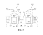
- FIG. 9 is schematic cross-sectional diagram showing a semiconductor device according to a third preferred embodiment of the present invention. Processes and structure according to this embodiment are substantially similar to those described in the first preferred embodiment. The main difference between these two embodiments is that the gate electrode 212 , the work function metal layer 216 and the dielectric layer 214 in each trench 210 are etched prior to the formation of the first mask layer 220 ′′. Therefore, a top recess 22 may be formed in the top portions of the trench 210 .
- the first mask layer 220 ′′ formed by oxidizing or nitriding the top surfaces of the gate electrode 212 , the work function metal layer 216 and the dielectric layer 214 may be completely covered by the first mask layer 220 ′′.
- the bottom surface of the first mask layer 220 ′′ may have a fourth width W 4 , which is equal to the total width of the gate electrode 212 , the work function metal layer 216 and the dielectric layer 214 .
- the bottom surface of the second mask layer 232 may have a second width W 2 , which is less than the fourth width W 4 of the first mask layers 220 ′′. Since other characteristics and advantages of the present modification are all similar to those described in the first preferred embodiment, their description is therefore omitted for the sake of clarity.
- the present invention may be also applied to other types of semiconductor devices without departing from the scope of the present invention.
- a portion of or all the metal gate structures may be replaced with resistor structures, capacitor structures, e-fused structures or other semiconductor devices.
- the self-aligned contact structure does not have to land between two adjacent metal gate structures, it also may land between two adjacent resistor structures or between a resistor structure and a metal gate structure, but not limited thereto.
- the first mask layer is formed through the oxidation or the nitridation process, and the second mask layer is optionally formed on the sides of the first mask layer. Because there is no need to remove an upper portion of the gate electrode and polish the gate electrode during or after the process for forming the first mask layer, the difference in height between the initial dummy gate structure and the final metal gate structure may be reduced. In this way, the height of the dummy gate structure at the beginning of the fabrication process may be effectively reduced and the height of the subsequent trench may also be reduced.
- the drawback of the dummy gate structure being prone to breaking may be overcome; the shadowing effect caused by the dummy gate structure during the ion implantation process may be avoided; the capability of filling the interlayer dielectric layer and the conductive layer respectively into each dummy gate structure and each trench may all be improved. Furthermore, since there is no need to remove the upper portion of the gate electrode, even though there are defects, such as void defects, existing in the gate electrode, etchants are still not able to reach and damage the structure under the gate electrode, such as dielectric layer or substrate, through the defect.
Abstract
Description
Claims (18)
Applications Claiming Priority (2)
| Application Number | Priority Date | Filing Date | Title |
|---|---|---|---|
| CN201510001982 | 2015-01-05 | ||
| CN201510001982.0A CN105826174B (en) | 2015-01-05 | 2015-01-05 | Semiconductor device and method for fabricating the same |
Publications (1)
| Publication Number | Publication Date |
|---|---|
| US9312356B1 true US9312356B1 (en) | 2016-04-12 |
Family
ID=55643293
Family Applications (1)
| Application Number | Title | Priority Date | Filing Date |
|---|---|---|---|
| US14/613,379 Active US9312356B1 (en) | 2015-01-05 | 2015-02-04 | Semiconductor device and manufacturing method thereof |
Country Status (2)
| Country | Link |
|---|---|
| US (1) | US9312356B1 (en) |
| CN (1) | CN105826174B (en) |
Cited By (4)
| Publication number | Priority date | Publication date | Assignee | Title |
|---|---|---|---|---|
| US20170162437A1 (en) * | 2015-12-07 | 2017-06-08 | International Business Machines Corporation | Middle of the line subtractive self-aligned contacts |
| US20180366552A1 (en) * | 2017-06-19 | 2018-12-20 | Samsung Electronics Co., Ltd. | Semiconductor device |
| US20190057895A1 (en) * | 2017-08-16 | 2019-02-21 | United Microelectronics Corp. | Manufacturing method of interconnect structure |
| US20220068713A1 (en) * | 2018-09-18 | 2022-03-03 | International Business Machines Corporation | Tiered-Profile Contact for Semiconductor |
Families Citing this family (3)
| Publication number | Priority date | Publication date | Assignee | Title |
|---|---|---|---|---|
| CN110299320B (en) * | 2018-03-21 | 2023-11-21 | 联华电子股份有限公司 | Semiconductor device and method for manufacturing the same |
| US11296023B2 (en) * | 2019-04-10 | 2022-04-05 | United Microelectronics Corp. | Semiconductor device and method of fabricating the same |
| US11476363B2 (en) | 2019-04-10 | 2022-10-18 | United Microelectronics Corp. | Semiconductor device and method of fabricating the same |
Citations (3)
| Publication number | Priority date | Publication date | Assignee | Title |
|---|---|---|---|---|
| US6797556B2 (en) * | 1999-12-30 | 2004-09-28 | Intel Corporation | MOS transistor structure and method of fabrication |
| US8802560B1 (en) | 2013-03-14 | 2014-08-12 | Taiwan Semiconductor Manufacturing Company, Ltd. | Method of fabricating an semiconductor interconnect structure |
| US20150008527A1 (en) | 2011-09-15 | 2015-01-08 | International Business Machines Corporation | Integrated circuit structure having selectively formed metal cap |
Family Cites Families (5)
| Publication number | Priority date | Publication date | Assignee | Title |
|---|---|---|---|---|
| US8048790B2 (en) * | 2009-09-17 | 2011-11-01 | Globalfoundries Inc. | Method for self-aligning a stop layer to a replacement gate for self-aligned contact integration |
| US8119473B2 (en) * | 2009-12-31 | 2012-02-21 | Taiwan Semiconductor Manufacturing Company, Ltd. | High temperature anneal for aluminum surface protection |
| US8822283B2 (en) * | 2011-09-02 | 2014-09-02 | Taiwan Semiconductor Manufacturing Company, Ltd. | Self-aligned insulated film for high-k metal gate device |
| US8772168B2 (en) * | 2012-01-19 | 2014-07-08 | Globalfoundries Singapore Pte. Ltd. | Formation of the dielectric cap layer for a replacement gate structure |
| US9006804B2 (en) * | 2013-06-06 | 2015-04-14 | United Microelectronics Corp. | Semiconductor device and fabrication method thereof |
-
2015
- 2015-01-05 CN CN201510001982.0A patent/CN105826174B/en active Active
- 2015-02-04 US US14/613,379 patent/US9312356B1/en active Active
Patent Citations (3)
| Publication number | Priority date | Publication date | Assignee | Title |
|---|---|---|---|---|
| US6797556B2 (en) * | 1999-12-30 | 2004-09-28 | Intel Corporation | MOS transistor structure and method of fabrication |
| US20150008527A1 (en) | 2011-09-15 | 2015-01-08 | International Business Machines Corporation | Integrated circuit structure having selectively formed metal cap |
| US8802560B1 (en) | 2013-03-14 | 2014-08-12 | Taiwan Semiconductor Manufacturing Company, Ltd. | Method of fabricating an semiconductor interconnect structure |
Non-Patent Citations (1)
| Title |
|---|
| Lin, Title of Invention: Method of fabricating metal gate structure, U.S. Appl. No. 14/463,677, filed Aug. 20, 2014. |
Cited By (8)
| Publication number | Priority date | Publication date | Assignee | Title |
|---|---|---|---|---|
| US20170162437A1 (en) * | 2015-12-07 | 2017-06-08 | International Business Machines Corporation | Middle of the line subtractive self-aligned contacts |
| US10032674B2 (en) | 2015-12-07 | 2018-07-24 | International Business Machines Corporation | Middle of the line subtractive self-aligned contacts |
| US10373874B2 (en) * | 2015-12-07 | 2019-08-06 | International Business Machines Corporation | Middle of the line subtractive self-aligned contacts |
| US10714393B2 (en) | 2015-12-07 | 2020-07-14 | International Business Machines Corporation | Middle of the line subtractive self-aligned contacts |
| US20180366552A1 (en) * | 2017-06-19 | 2018-12-20 | Samsung Electronics Co., Ltd. | Semiconductor device |
| US20190057895A1 (en) * | 2017-08-16 | 2019-02-21 | United Microelectronics Corp. | Manufacturing method of interconnect structure |
| US10497607B2 (en) * | 2017-08-16 | 2019-12-03 | United Microelectronics Corp. | Manufacturing method of interconnect structure |
| US20220068713A1 (en) * | 2018-09-18 | 2022-03-03 | International Business Machines Corporation | Tiered-Profile Contact for Semiconductor |
Also Published As
| Publication number | Publication date |
|---|---|
| CN105826174B (en) | 2021-06-15 |
| CN105826174A (en) | 2016-08-03 |
Similar Documents
| Publication | Publication Date | Title |
|---|---|---|
| US9281199B2 (en) | Method for fabricating semiconductor device with paterned hard mask | |
| US10332978B2 (en) | Device with reinforced metal gate spacer and method of fabricating | |
| US9530862B2 (en) | Semiconductor device having metal gate and manufacturing method thereof | |
| US9312356B1 (en) | Semiconductor device and manufacturing method thereof | |
| US9117886B2 (en) | Method for fabricating a semiconductor device by forming and removing a dummy gate structure | |
| US8765546B1 (en) | Method for fabricating fin-shaped field-effect transistor | |
| US9024393B2 (en) | Manufacturing method for semiconductor device having metal gate | |
| US8981527B2 (en) | Resistor and manufacturing method thereof | |
| US9711411B2 (en) | Semiconductor device and method for fabricating the same | |
| US8692334B2 (en) | Resistor integrated with transistor having metal gate | |
| US8477006B2 (en) | Resistor and manufacturing method thereof | |
| US20150118836A1 (en) | Method of fabricating semiconductor device | |
| US20130099307A1 (en) | Semiconductor device having metal gate and manufacturing method thereof | |
| US20130105903A1 (en) | Semiconductor device having metal gate and manufacturing method thereof | |
| US9496361B1 (en) | Selectively deposited metal gates and method of manufacturing thereof | |
| US8551876B2 (en) | Manufacturing method for semiconductor device having metal gate | |
| US9105623B2 (en) | Semiconductor device having metal gate and manufacturing method thereof | |
| US8710593B2 (en) | Resistor and manufacturing method thereof | |
| US11545560B2 (en) | Semiconductor device and method for fabricating the same | |
| US9543203B1 (en) | Method of fabricating a semiconductor structure with a self-aligned contact | |
| US20140113425A1 (en) | Method of fabricating semiconductor device | |
| TWI533360B (en) | Semiconductor device having metal gate and manufacturing method thereof | |
| TW201310577A (en) | Resistor and manufacturing method thereof | |
| TWI520307B (en) | Resistor and manufacturing method thereof |
Legal Events
| Date | Code | Title | Description |
|---|---|---|---|
| AS | Assignment |
Owner name: UNITED MICROELECTRONICS CORP., TAIWAN Free format text: ASSIGNMENT OF ASSIGNORS INTEREST;ASSIGNORS:LIN, CHING-LING;HUANG, CHIH-SEN;CHEN, YI-WEN;REEL/FRAME:034881/0628 Effective date: 20150130 |
|
| STCF | Information on status: patent grant |
Free format text: PATENTED CASE |
|
| MAFP | Maintenance fee payment |
Free format text: PAYMENT OF MAINTENANCE FEE, 4TH YEAR, LARGE ENTITY (ORIGINAL EVENT CODE: M1551); ENTITY STATUS OF PATENT OWNER: LARGE ENTITY Year of fee payment: 4 |
|
| MAFP | Maintenance fee payment |
Free format text: PAYMENT OF MAINTENANCE FEE, 8TH YEAR, LARGE ENTITY (ORIGINAL EVENT CODE: M1552); ENTITY STATUS OF PATENT OWNER: LARGE ENTITY Year of fee payment: 8 |