US9305834B1 - Methods for fabricating integrated circuits using designs of integrated circuits adapted to directed self-assembly fabrication to form via and contact structures - Google Patents
Methods for fabricating integrated circuits using designs of integrated circuits adapted to directed self-assembly fabrication to form via and contact structures Download PDFInfo
- Publication number
- US9305834B1 US9305834B1 US14/586,268 US201414586268A US9305834B1 US 9305834 B1 US9305834 B1 US 9305834B1 US 201414586268 A US201414586268 A US 201414586268A US 9305834 B1 US9305834 B1 US 9305834B1
- Authority
- US
- United States
- Prior art keywords
- integrated circuit
- layer
- feature pitch
- features
- determining
- Prior art date
- Legal status (The legal status is an assumption and is not a legal conclusion. Google has not performed a legal analysis and makes no representation as to the accuracy of the status listed.)
- Active
Links
- 238000000034 method Methods 0.000 title claims abstract description 110
- 238000013461 design Methods 0.000 title claims abstract description 77
- 238000002408 directed self-assembly Methods 0.000 title claims abstract description 57
- 238000004519 manufacturing process Methods 0.000 title description 15
- 229920001400 block copolymer Polymers 0.000 claims abstract description 70
- 239000000463 material Substances 0.000 claims abstract description 61
- 239000004065 semiconductor Substances 0.000 claims abstract description 25
- 238000000926 separation method Methods 0.000 claims abstract description 24
- 230000015572 biosynthetic process Effects 0.000 claims abstract description 8
- 238000001459 lithography Methods 0.000 claims description 17
- 229920002120 photoresistant polymer Polymers 0.000 claims description 16
- 238000001465 metallisation Methods 0.000 claims description 14
- 239000004020 conductor Substances 0.000 claims description 5
- 238000000059 patterning Methods 0.000 claims description 4
- -1 poly(2-vinyl pyridine) Polymers 0.000 claims description 4
- 238000005530 etching Methods 0.000 claims description 3
- 238000000206 photolithography Methods 0.000 claims description 3
- 229920003171 Poly (ethylene oxide) Polymers 0.000 claims description 2
- 239000005062 Polybutadiene Substances 0.000 claims description 2
- 239000004205 dimethyl polysiloxane Substances 0.000 claims description 2
- 229920000885 poly(2-vinylpyridine) Polymers 0.000 claims description 2
- 229920000435 poly(dimethylsiloxane) Polymers 0.000 claims description 2
- 229920003229 poly(methyl methacrylate) Polymers 0.000 claims description 2
- 229920002857 polybutadiene Polymers 0.000 claims description 2
- 239000004926 polymethyl methacrylate Substances 0.000 claims description 2
- 238000001900 extreme ultraviolet lithography Methods 0.000 claims 1
- 239000010410 layer Substances 0.000 description 106
- 239000011295 pitch Substances 0.000 description 41
- 229920000642 polymer Polymers 0.000 description 18
- 239000000126 substance Substances 0.000 description 5
- 238000010420 art technique Methods 0.000 description 3
- 229910052751 metal Inorganic materials 0.000 description 3
- 239000002184 metal Substances 0.000 description 3
- RYGMFSIKBFXOCR-UHFFFAOYSA-N Copper Chemical compound [Cu] RYGMFSIKBFXOCR-UHFFFAOYSA-N 0.000 description 2
- BOTDANWDWHJENH-UHFFFAOYSA-N Tetraethyl orthosilicate Chemical compound CCO[Si](OCC)(OCC)OCC BOTDANWDWHJENH-UHFFFAOYSA-N 0.000 description 2
- 238000013459 approach Methods 0.000 description 2
- 238000005229 chemical vapour deposition Methods 0.000 description 2
- 229910052802 copper Inorganic materials 0.000 description 2
- 239000010949 copper Substances 0.000 description 2
- 238000000151 deposition Methods 0.000 description 2
- 239000003989 dielectric material Substances 0.000 description 2
- 229920001519 homopolymer Polymers 0.000 description 2
- 238000001020 plasma etching Methods 0.000 description 2
- 238000001338 self-assembly Methods 0.000 description 2
- 208000031481 Pathologic Constriction Diseases 0.000 description 1
- 229910052581 Si3N4 Inorganic materials 0.000 description 1
- VYPSYNLAJGMNEJ-UHFFFAOYSA-N Silicium dioxide Chemical compound O=[Si]=O VYPSYNLAJGMNEJ-UHFFFAOYSA-N 0.000 description 1
- XUIMIQQOPSSXEZ-UHFFFAOYSA-N Silicon Chemical compound [Si] XUIMIQQOPSSXEZ-UHFFFAOYSA-N 0.000 description 1
- 229910052782 aluminium Inorganic materials 0.000 description 1
- XAGFODPZIPBFFR-UHFFFAOYSA-N aluminium Chemical compound [Al] XAGFODPZIPBFFR-UHFFFAOYSA-N 0.000 description 1
- 238000000137 annealing Methods 0.000 description 1
- 238000007796 conventional method Methods 0.000 description 1
- 238000012937 correction Methods 0.000 description 1
- 230000003247 decreasing effect Effects 0.000 description 1
- 230000002950 deficient Effects 0.000 description 1
- 238000000407 epitaxy Methods 0.000 description 1
- 230000006870 function Effects 0.000 description 1
- 239000011229 interlayer Substances 0.000 description 1
- 229920002521 macromolecule Polymers 0.000 description 1
- 230000003287 optical effect Effects 0.000 description 1
- 238000005191 phase separation Methods 0.000 description 1
- 238000000623 plasma-assisted chemical vapour deposition Methods 0.000 description 1
- 239000000376 reactant Substances 0.000 description 1
- 239000005368 silicate glass Substances 0.000 description 1
- 229910052710 silicon Inorganic materials 0.000 description 1
- 239000010703 silicon Substances 0.000 description 1
- HQVNEWCFYHHQES-UHFFFAOYSA-N silicon nitride Chemical compound N12[Si]34N5[Si]62N3[Si]51N64 HQVNEWCFYHHQES-UHFFFAOYSA-N 0.000 description 1
- 229910052814 silicon oxide Inorganic materials 0.000 description 1
- 238000012546 transfer Methods 0.000 description 1
- WFKWXMTUELFFGS-UHFFFAOYSA-N tungsten Chemical compound [W] WFKWXMTUELFFGS-UHFFFAOYSA-N 0.000 description 1
- 229910052721 tungsten Inorganic materials 0.000 description 1
- 239000010937 tungsten Substances 0.000 description 1
Images


Classifications
-
- H—ELECTRICITY
- H01—ELECTRIC ELEMENTS
- H01L—SEMICONDUCTOR DEVICES NOT COVERED BY CLASS H10
- H01L21/00—Processes or apparatus adapted for the manufacture or treatment of semiconductor or solid state devices or of parts thereof
- H01L21/70—Manufacture or treatment of devices consisting of a plurality of solid state components formed in or on a common substrate or of parts thereof; Manufacture of integrated circuit devices or of parts thereof
- H01L21/71—Manufacture of specific parts of devices defined in group H01L21/70
- H01L21/768—Applying interconnections to be used for carrying current between separate components within a device comprising conductors and dielectrics
- H01L21/76838—Applying interconnections to be used for carrying current between separate components within a device comprising conductors and dielectrics characterised by the formation and the after-treatment of the conductors
- H01L21/76841—Barrier, adhesion or liner layers
- H01L21/76853—Barrier, adhesion or liner layers characterized by particular after-treatment steps
-
- H—ELECTRICITY
- H01—ELECTRIC ELEMENTS
- H01L—SEMICONDUCTOR DEVICES NOT COVERED BY CLASS H10
- H01L21/00—Processes or apparatus adapted for the manufacture or treatment of semiconductor or solid state devices or of parts thereof
- H01L21/70—Manufacture or treatment of devices consisting of a plurality of solid state components formed in or on a common substrate or of parts thereof; Manufacture of integrated circuit devices or of parts thereof
- H01L21/71—Manufacture of specific parts of devices defined in group H01L21/70
- H01L21/768—Applying interconnections to be used for carrying current between separate components within a device comprising conductors and dielectrics
- H01L21/76801—Applying interconnections to be used for carrying current between separate components within a device comprising conductors and dielectrics characterised by the formation and the after-treatment of the dielectrics, e.g. smoothing
- H01L21/76802—Applying interconnections to be used for carrying current between separate components within a device comprising conductors and dielectrics characterised by the formation and the after-treatment of the dielectrics, e.g. smoothing by forming openings in dielectrics
- H01L21/76816—Aspects relating to the layout of the pattern or to the size of vias or trenches
-
- G—PHYSICS
- G03—PHOTOGRAPHY; CINEMATOGRAPHY; ANALOGOUS TECHNIQUES USING WAVES OTHER THAN OPTICAL WAVES; ELECTROGRAPHY; HOLOGRAPHY
- G03F—PHOTOMECHANICAL PRODUCTION OF TEXTURED OR PATTERNED SURFACES, e.g. FOR PRINTING, FOR PROCESSING OF SEMICONDUCTOR DEVICES; MATERIALS THEREFOR; ORIGINALS THEREFOR; APPARATUS SPECIALLY ADAPTED THEREFOR
- G03F7/00—Photomechanical, e.g. photolithographic, production of textured or patterned surfaces, e.g. printing surfaces; Materials therefor, e.g. comprising photoresists; Apparatus specially adapted therefor
- G03F7/0002—Lithographic processes using patterning methods other than those involving the exposure to radiation, e.g. by stamping
-
- H—ELECTRICITY
- H01—ELECTRIC ELEMENTS
- H01L—SEMICONDUCTOR DEVICES NOT COVERED BY CLASS H10
- H01L21/00—Processes or apparatus adapted for the manufacture or treatment of semiconductor or solid state devices or of parts thereof
- H01L21/02—Manufacture or treatment of semiconductor devices or of parts thereof
- H01L21/04—Manufacture or treatment of semiconductor devices or of parts thereof the devices having potential barriers, e.g. a PN junction, depletion layer or carrier concentration layer
- H01L21/18—Manufacture or treatment of semiconductor devices or of parts thereof the devices having potential barriers, e.g. a PN junction, depletion layer or carrier concentration layer the devices having semiconductor bodies comprising elements of Group IV of the Periodic Table or AIIIBV compounds with or without impurities, e.g. doping materials
- H01L21/30—Treatment of semiconductor bodies using processes or apparatus not provided for in groups H01L21/20 - H01L21/26
- H01L21/31—Treatment of semiconductor bodies using processes or apparatus not provided for in groups H01L21/20 - H01L21/26 to form insulating layers thereon, e.g. for masking or by using photolithographic techniques; After treatment of these layers; Selection of materials for these layers
- H01L21/3105—After-treatment
- H01L21/311—Etching the insulating layers by chemical or physical means
- H01L21/31144—Etching the insulating layers by chemical or physical means using masks
-
- H—ELECTRICITY
- H01—ELECTRIC ELEMENTS
- H01L—SEMICONDUCTOR DEVICES NOT COVERED BY CLASS H10
- H01L21/00—Processes or apparatus adapted for the manufacture or treatment of semiconductor or solid state devices or of parts thereof
- H01L21/70—Manufacture or treatment of devices consisting of a plurality of solid state components formed in or on a common substrate or of parts thereof; Manufacture of integrated circuit devices or of parts thereof
- H01L21/71—Manufacture of specific parts of devices defined in group H01L21/70
- H01L21/768—Applying interconnections to be used for carrying current between separate components within a device comprising conductors and dielectrics
- H01L21/76838—Applying interconnections to be used for carrying current between separate components within a device comprising conductors and dielectrics characterised by the formation and the after-treatment of the conductors
- H01L21/76841—Barrier, adhesion or liner layers
- H01L21/76867—Barrier, adhesion or liner layers characterized by methods of formation other than PVD, CVD or deposition from a liquids
-
- H—ELECTRICITY
- H01—ELECTRIC ELEMENTS
- H01L—SEMICONDUCTOR DEVICES NOT COVERED BY CLASS H10
- H01L27/00—Devices consisting of a plurality of semiconductor or other solid-state components formed in or on a common substrate
- H01L27/02—Devices consisting of a plurality of semiconductor or other solid-state components formed in or on a common substrate including semiconductor components specially adapted for rectifying, oscillating, amplifying or switching and having potential barriers; including integrated passive circuit elements having potential barriers
- H01L27/0203—Particular design considerations for integrated circuits
- H01L27/0207—Geometrical layout of the components, e.g. computer aided design; custom LSI, semi-custom LSI, standard cell technique
Definitions
- the technical field relates generally to methods for fabricating integrated circuits. More particularly, the technical field relates to methods for fabricating integrated circuits using directed self-assembly to form via and contact structures.
- Optical lithography has been a driving force for device scaling.
- Conventional optical lithography is limited to about 80 nanometer (nm) pitch for single exposure patterning. While double and other multi-patterning processes can realize smaller pitch, these approaches are expensive and more complex.
- Directed self-assembly a technique that aligns self-assembling polymeric materials on a lithographically-defined directing or guide pattern, is a potential option for extending current lithography beyond its pitch and resolution limits.
- the self-assembling materials for example, are block copolymers (BCPs) that include an “A” homopolymer covalently bonded to a “B” homopolymer, which are deposited over a lithographically-defined directing pattern on a semiconductor wafer-in-process or work-in-process (WIP).
- the lithographically-defined directing pattern is a pre-pattern (hereinafter “DSA directing pattern”) that is encoded with spatial chemical and/or topographical information (e.g., chemical epitaxy and/or graphoepitaxy) and serves to direct the self-assembly process and the pattern formed by the self-assembling materials. Subsequently, by annealing the DSA polymers, the A polymer chains and the B polymer chains undergo micro-phase separation to form an A polymer region and a B polymer region that are registered to the underlying DSA directing pattern to define a nano-pattern (hereinafter “DSA pattern”).
- DSA pattern a pre-pattern
- topographical information e.g., chemical epitaxy and/or graphoepitaxy
- a and B polymer regions are formed due to the intra- and inter-molecular forces exerted by the block copolymer macromolecules.
- the dimensions of these polymer regions are determined by the characteristic dimensions of the block copolymer molecules, resulting in a formation of structures with dimensions at a smaller scale compared to DSA directing patterns. Then, by removing either the A polymer block or the B polymer block by wet chemical or plasma-etch techniques, a mask is formed for transferring the DSA pattern to the underlying semiconductor WIP.
- One DSA technique is graphoepitaxy in which self-assembly is directed by topographical features that are formed overlying a semiconductor WIP.
- This technique is used, for example, to create via and contact holes that can be subsequently filled with conductive material for forming electrical connections between one or more layers of the semiconductor WIP.
- the topographical features are formed overlying the semiconductor WIP using a photomask that defines mask features and conventional lithographic techniques to transfer the mask features to a photoresist layer that overlies the semiconductor WIP to form a patterned photoresist layer.
- the developed photoresist pattern can be used as is or further etched into underlying layers to form the topographical features that define confinement wells.
- FIG. 1A illustrates a semiconductor WIP 101 that has a patterned photoresist material layer 102 formed thereover to define a plurality of confinement wells 103 .
- the confinement wells are filled with a BCP that is subsequently micro-phase separated to form, for example, selectively etchable cylinders or other etchable features that are each formed of either the A polymer region or the B polymer region of the BCP.
- the etchable cylinders are removed to form openings and define a mask for etch transferring the openings to the underlying semiconductor WIP for the formation of via and contact holes.
- FIG. 1B illustrates the semiconductor WIP 101 of FIG. 1A after the confinement wells 103 have been filled with a BCP and after the BCP has micro-phase separated into a plurality of cylindrical polymer A regions 104 and polymer B regions 105 surrounding the polymer A regions 104 .
- cylindrical polymer regions formed in the BCP film in the manner described above typically self-assemble in hexagonally-arranged patterns, as shown in FIG. 2 .
- a hexagon we mean a regular hexagon, that is a polygon with six vertices and six edges of equal lengths and with all internal angles equal to 120 degrees.
- a hexagonal overlay 200 is superimposed on the cylindrical polymer A regions 104 in FIG. 2 to better illustrate this configuration.
- the length of each side of the hexagonal overlay represents the natural, hexagonal separation distance between cylinders (defined from the center-point of each cylinder), which is commonly referred to in the art as separation distance L 0 , as illustrated.
- FIG. 3 illustrates a complex-shaped confinement well 303 that has been used to attempt to match a BCP cylinder pattern with a desired layout pattern.
- a plurality of cylinders 312 and 313 are illustrated in the confinement well 303 , and the desired layout pattern is illustrated by a plurality of via/contact structures 311 on to the confinement well 303 .
- cylinders 312 are undesirably out of alignment from via/contacts structures 311 .
- cylinders 313 are formed where no via/contact structure was intended. Only at locations 314 , in this example, do the cylinders and the pattern layout of via/contact structures substantially up.
- confinement well 303 makes an attempt to match all cylinders with the desired pattern layout, the shortcomings of using only the confinement well to direct the cylinder placement are manifest.
- the method further includes generating an integrated circuit layout design wherein integrated circuit features are spaced in accordance with the integrated circuit feature pitch P A and wherein via or contact structures are physically and electrically connected to the integrated circuit features and fabricating the integrated circuit features and the via or contact structures on a semiconductor work-in-process (WIP) in accordance with the integrated circuit layout design, wherein the via or contact structures are fabricated utilizing DSA with the BCP material.
- WIP semiconductor work-in-process
- a method for fabricating an integrated circuit includes determining an integrated circuit feature pitch P A , wherein P A is greater than or equal to a minimum lithography pitch used to pattern confinement wells for enclosing a block copolymer (BCP) material during directed self-assembly (DSA) and generating an integrated circuit layout design wherein integrated circuit features are spaced in accordance with the integrated circuit feature pitch P A and wherein via or contact structures are physically and electrically connected to the integrated circuit features.
- the method further includes fabricating the integrated circuit features and the via or contact structures on a semiconductor work-in-process (WIP) in accordance with the integrated circuit layout design, wherein the via or contact structures are fabricated utilizing DSA with the BCP material.
- WIP semiconductor work-in-process
- a method for fabricating an integrated circuit includes determining a natural, hexagonal separation distance L 0 between cylinders formed in a block copolymer (BCP) material during directed self-assembly (DSA), determining an integrated circuit feature pitch P A of a first layer of the integrated circuit as either greater than or equal to a minimum lithography pitch used to pattern confinement wells for enclosing the BCP material during DSA or equal to L 0 *(sqrt(3)/2)*n, wherein n is a positive integer, and determining an integrated circuit feature pitch P B of a second layer of the integrated circuit as equal to either (L 0 /2)*m or L 0 *(sqrt(3)/2)*m, wherein m is a positive integer selected independently from n, and wherein the first layer of the integrated circuit is disposed above or below the second layer of the integrated circuit.
- BCP block copolymer
- DSA directed self-assembly
- the method further includes generating an integrated circuit layout design wherein integrated circuit features of the first layer of the integrated circuit are spaced in accordance with the integrated circuit feature pitch P A , wherein integrated circuit features of the second layer of the integrated circuit are spaced in accordance with the integrated circuit feature pitch P B , and wherein via or contact structures are physically and electrically connected between the integrated circuit features of both the first and second layers of the integrated circuit and fabricating the integrated circuit features and the via or contact structures on a semiconductor work-in-process (WIP) in accordance with the integrated circuit layout design, wherein the via or contact structures are fabricated utilizing DSA with the BCP material.
- WIP semiconductor work-in-process
- FIGS. 1A and 1B illustrate the formation of polymeric cylinders over a semiconductor WIP in accordance with processes known in the prior art
- FIG. 2 illustrates the natural, hexagonal arrangement of polymeric cylinders as known in the prior art
- FIG. 3 illustrates the use of a complex-patterned confinement well to adjust the natural arrangement of polymeric cylinders to more closely match a desired integrated circuit design layout in accordance with processes known in the prior art
- FIG. 4 illustrates an exemplary integrated circuit environment in which the various embodiments of the present disclosure may be implemented
- FIGS. 5-9 illustrate “DSA-aware” integrated circuit design principles with regard to the placement of via and contact structures in accordance with various exemplary embodiments of the present disclosure.
- FIGS. 10-15 provide integrated circuit structures and methods for fabrication of integrated circuit structures using the “DSA-aware” integrated circuit design principles of FIGS. 5-9 in accordance with various exemplary embodiments of the present disclosure.
- Embodiments of the present disclosure are generally directed to methods for fabricating integrated circuits using directed self-assembly to form via and contact structures.
- conventional techniques related to integrated circuit device fabrication may not be described in detail herein.
- the various tasks and process steps described herein may be incorporated into a more comprehensive procedure or process having additional steps or functionality not described in detail herein.
- steps in the manufacture of semiconductor-based memory structures are well-known and so, in the interest of brevity, many conventional steps will only be mentioned briefly herein or will be omitted entirely without providing the well-known process details.
- via and/or contact structures which may be subsequently filled with conductive material to form conductive connecting structures (i.e., vias and contacts) of the integrated circuit.
- via is generally used when referring to a conductive connecting structure that provides an electrical connection between two metallization layers, such as may be formed during back-end-of-line (BEOL) fabrication processes.
- contact is generally used when referring to a conductive connecting structure that provides an electrical connection between an active integrated circuit structure, such as a transistor (i.e., the gate electrode or the source/drain areas thereof), and an overlying metallization layer.
- FIG. 1 For ease of illustration, the Figures described in greater detail below illustrate certain embodiments in the context of fabricating a via structure, i.e., a conductive element between two metallization layers. However, it will be appreciated that these embodiments may be alternatively implemented in the context of fabricating a contact structure, i.e., a conductive element between an active integrated circuit structure and a metallization layer.
- FIG. 4 illustrates an exemplary integrated circuit environment in which the various embodiments of the present disclosure may be implemented.
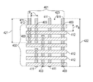
- FIG. 4 generally illustrates a first layer 401 of an integrated circuit and a second layer 402 of the integrated circuit. Assuming that FIG. 4 is a top view of the layers 401 and 402 , it will be appreciated that second layer 402 is disposed so as to be overlying first layer 401 .
- Providing electrical connection between the layers 401 and 402 is a plurality of electrical connection structures 403 , which in various embodiments may be either vias or contacts. Electrical connection structures 403 provide an electrical path connecting the layers 401 and 402 .
- the spatially relative terms are intended to encompass different orientations of the device in use or operation in addition to the orientation depicted in the figures. For example, if the integrated circuit layout design in the figures is turned over, elements described as being “below” or “beneath” other elements or features would then be oriented “above” the other elements or features. Thus, the exemplary term “below” can encompass both an orientation of above and below.
- the device may be otherwise oriented (rotated 90 degrees or at other orientations) and the spatially relative descriptors used herein may likewise be interpreted accordingly.
- layers 401 and 402 are understood to be metallization layers (e.g., M 1 , M 2 , M 3 , etc.) of the integrated circuit.
- metallization layers e.g., M 1 , M 2 , M 3 , etc.
- individual integrated circuit features 411 which are hereinafter referred to as integrated circuit feature “lines” 411 of layer 401 , in this embodiment, are parallel conductive lines of a metallization layer.
- individual feature lines 412 of layer 402 are parallel conductive lines of an overlying metallization layer.
- feature lines 411 of layer 401 may represent active features/structures of the integrated circuit, such as a gate electrode or source/drain structures, and feature lines 412 of layer 402 represent parallel conductive lines of an overlying metallization layer, such as M 1 .
- the feature lines 411 of layer 401 and the feature lines 412 of layer 402 may run substantially perpendicularly with respect to one another, which is a common feature of modern integrated circuit design principles.
- the term “substantially” refers to the complete, or nearly complete, extent or degree of an action, characteristic, property, state, structure, item, or result.
- an object that is “substantially” enclosed would mean that the object is either completely enclosed or nearly completely enclosed. The exact allowable degree of deviation from absolute completeness may in some cases depend on the specific context. However, generally speaking the nearness of completion will be so as to have the same overall result as if absolute and total completion were obtained.
- the feature lines 411 and 412 need not run perpendicularly with respect to one another, but may run at another angle, such as about 60 degrees as described in greater detail below in connection with FIG. 6 .
- the feature lines need not all be the same length, and some may be not present or may be “missing.”
- layer 401 illustrates feature lines 411 of various lengths, i.e., compare length 421 with length 422 of feature lines 411 .
- a feature line 411 is not present.
- feature lines 412 like 411 , may be of various lengths or may be missing. The various lengths and presence of feature lines 411 and 412 will vary greatly depending on the particular integrated circuit design, and should not be understood as a limiting feature of the presently described embodiments.
- FIG. 4 illustrates an integrated circuit feature line pitch P A of the layer 401 and an integrated circuit feature line pitch P B of the layer 402 .
- P A refers to the pitch of the overlying or the underlying layer, and the designation of one layer's pitch as P A and the other's as P B should not be understood as a limiting feature of the presently described embodiments. That is, the first layer 401 having feature pitch P A may, in various embodiments, be understood as being either above or below the second layer 402 having feature pitch P B . As shown in FIG.
- the term “pitch” is used to define the separation distance between adjacent feature lines, wherein measuring the separation distance is performed at the same location of each line (i.e., the right-most edge thereof for lines 411 and the top-most edge thereof for lines 412 as shown in FIG. 4 ).
- the separation distance becomes 2*P A , and so on.
- FIGS. 5-9 Various embodiments if the present disclosure will now be described in connection with FIGS. 5-9 . It should be appreciated that the foregoing discussion of FIG. 4 concerning the exemplary semiconductor environment, e.g. line configuration and lengths, pitches, electrical connection structures, etc. is applicable to each of the following FIGS. 5-9 , and as such the foregoing description will not be repeated with regard to each such Figure for brevity of discussion.
- a “DSA-aware” integrated circuit layout design is created by setting P A equal to L 0 *(sqrt(3)/2)*n, wherein n is a positive integer.
- the tolerance ⁇ is a value determined by those having ordinary skill in the art based on knowledge of particular DSA processes and BCP material selected for use, but may generally be within one of 20%, 10%, 5%, or 1% of the exact numerical value. For example, if the skilled artisan knows that a particular DSA process with a particular BCP tends to exhibit an approximate 10% variance from perfect geometric (hexagonal) order, then selecting ⁇ to be 10% of the exact numerical value of ⁇ 0.866025, and thus implying that the term “sqrt(3)/2” has a meaning of ⁇ 0.866025+/ ⁇ 10%, would be appropriate under such circumstances. In sum, the present disclosure should not be read as requiring a strict geometric ratio (i.e., exact numerical value of sqrt(3)/2) for implementation when the nature of DSA using BCP material typically does not allow for such stricture.
- an exemplary method for fabricating an integrated circuit includes determining the natural, hexagonal separation distance L 0 between cylinders formed in a block copolymer material during directed self-assembly (DSA). This determination may be made based upon the particular BCP material selection, various examples of which are provided in greater detail below. Moreover, the BCP material selection may be based on a desired L 0 distance, which may be pre-determined according to the constraints of the fabrication process or according to a desired integrated circuit layout spacing. That is, the IC design and angles may be first determined, and then the appropriate BCP material selected in accordance with such IC design. As initially noted above, the order of performing these steps in the methods is not critical.
- integrated circuit layout designs can be generated in several different formats.
- the Graphic Data System II (GDSII) format is a popular format for transferring and archiving two-dimensional (2D) graphical circuit layout data. Among other features, it contains a hierarchy of structures, each structure containing layout elements (e.g., polygons, paths or poly-lines, circles and textboxes).
- Other formats include the more recent Open Artwork System Interchange Standard (OASIS) proposed by Semiconductor Equipment and Materials International (SEMI), for example. These various industry formats are used to define the geometrical information in design layouts that are employed to manufacture integrated circuits.
- OASIS Open Artwork System Inter
- a “DSA-aware” integrated circuit layout design is created by setting P A greater than or equal to the minimum lithography pitch used to pattern confinement wells for enclosing the block copolymer material during directed self-assembly.
- a method for fabricating an integrated circuit includes determining the via or contact hole separation distance P A as greater than or equal to a minimum lithography pitch used to pattern confinement wells for enclosing a block copolymer material during directed self-assembly and generating an integrated circuit layout design wherein vias or contact holes are separated in accordance with the via or contact hole separation distance P A .
- the layout design includes a first layer 501 that includes a plurality of feature lines 511 and a second layer 502 , overlying the first layer 501 , which includes a plurality of feature lines 512 , wherein the feature lines 511 and 512 run substantially perpendicularly with respect to one another.
- feature lines 511 or 512 and as generally applicable to all of the following-described embodiments such as in FIGS. 6, 8, and 9 ), it will be appreciated that these feature lines are illustrated, for simplicity, without cuts, or without the terminating metal wires.
- the pitch of the feature lines 511 , P A is set to equal L 0 *(sqrt(3)/2)*n, wherein n is a positive integer. In the illustrated embodiment, n is equal to 1, and as such P A equals L 0 *(sqrt(3)/2).
- the pitch of the feature lines 512 , P B is set to (L 0 /2)*m, wherein m is a positive integer selected independently from n.
- m is equal to 1, and as such P B equals L 0 /2.
- n and/or m higher than those specified may require the placement of “idle” or non-connected vias and contact structures between but not connected to either of feature lines, e.g. 511 and 512 , as shown in FIG. 5 .
- the term “idle” via or contact structure refers to a via or contact structure that provides no electrical connection between overlying integrated circuit layers, and as such is connected to the line features of at most one integrated circuit layer.
- Electrically connecting the layers 501 and 502 are a plurality of via or contact structures 503 , which are formed in a plurality of DSA confinement wells 505 that were previously patterned using conventional lithographic techniques.
- intersection refers to the apparent crossing of two feature lines in two different layers when viewed from above, even though it is understood that the feature lines do not in fact actually touch one another; rather, a conductive via or contact structure is used to provide electrical connection between the lines at the point of intersection. Accordingly, as shown in FIG. 5 , for a given line 511 , a via or contact structure 503 may be placed at the intersection of every other feature line 512 thereover, and for a given line 512 , a via or contact structure 503 may be placed at the intersection of every other feature line 511 thereunder. Whether a particular intersection has a via or contact structure providing electrical connection depends on the confinement well 505 pattern, which in turn depends on the integrated circuit layout design.
- Spacing the feature lines 511 and 512 according to the natural, hexagonal arrangement of the BCP cylinders, as opposed to attempting to fit the arrangement of the cylinders to a desired spacing, allows for the creation of a “DSA-aware” integrated circuit layout design that allows the BCP cylinders to form according to their natural order, and avoids prior art techniques that may resulting in the misalignment of vias or contacts as described above with regard to FIG. 3 .
- the layout design includes a first layer 601 that includes a plurality of feature lines 611 and a second layer 602 , overlying the first layer 601 , which includes a plurality of feature lines 612 .
- the feature lines 611 and 612 do not run substantially perpendicularly with respect to one another, but rather the feature lines 611 are oriented in a first direction and the feature lines 612 are oriented in a second direction that is angled with respect to the first direction such that cylinders connected to the layer 601 and separated from one another by the separation distance L 0 are also connected to the second layer of the integrated circuit.
- this angle 617 will typically be from about 50 degrees to about 70 degrees, such as about 60 degrees.
- the pitch of the feature lines 611 , P A is set to equal L 0 *(sqrt(3)/2)*n, wherein n is a positive integer. In the illustrated embodiment, n is equal to 1, and as such P A equals L 0 *(sqrt(3)/2).
- the pitch of the feature lines 612 , P B is set to L 0 *(sqrt(3)/2)*m, wherein m is a positive integer selected independently from n. In this illustrated embodiment, m is equal to 1 and as such P B equals L 0 *(sqrt(3)/2). Electrically connecting the layers 601 and 602 are a plurality of via or contact structures 603 , which are formed in a plurality of DSA confinement wells 605 that were previously patterned using conventional lithographic techniques.
- FIG. 7A provides two exemplary cell arrangements 751 and 752 , each of which includes a plurality of cells 730 that are suitable for use in connection with the integrated circuit layout design of FIG. 6 . As shown in FIG.
- cell arrangement 751 provides a “staggered” cell design, wherein the edges of adjacent cells are not coterminous with one another but are staggered to allow each cell to run at the same angle.
- Cell arrangement 752 provides coterminous cells in a “wave” pattern, wherein adjacent cells run at mirror-image angles with respect to one another, as opposed to at the same angle as in arrangement 751 .
- Other suitable cell arrangements may also be realized by those having ordinary skill in the art, and may be useful in connection with the layout design described above with regard to FIG. 6 .
- FIG. 7B illustrated is a representation of how a rectangular standard cell 775 can be designed, including feature lines 711 and 712 , wherein the feature lines 711 run at the above-described angle 617 .
- all features lines 711 and 712 are contained within the bounds of the standard cell 772 , causing the feature lines 711 in corner regions 776 a , 776 b of the standard cell 775 to be shorter than those that run through the center of the standard cell (with increasing lengths possible from the corners to the center).
- feature lines 712 like 711 , may be of various lengths or may be missing.
- Such rectangular standard cells 775 can be staggered as usual.
- the layout design includes a first layer 801 that includes a plurality of feature lines 811 and a second layer 802 , overlying the first layer 801 , which includes a plurality of feature lines 812 .
- the feature lines 811 and 812 run substantially perpendicularly with respect to one another.
- the pitch of the feature lines 811 , P A is set to equal L 0 *(sqrt(3)/2)*n, wherein n is a positive integer. In the illustrated embodiment, n is equal to 2, and as such P A equals L 0 *(sqrt(3)).
- the pitch of the feature lines 812 , P B is set to (L 0 /2)*m, wherein m is a positive integer selected independently from n. In this illustrated embodiment, m is equal to 2, and as such P B equals L 0 . Electrically connecting the layers 801 and 802 are a plurality of via or contact structures 803 , which are formed in a plurality of DSA confinement wells 805 that were previously patterned using conventional lithographic techniques.
- the term “idle” via or contact structure refers to a via or contact structure that provides no electrical connection between overlying integrated circuit layers, and as such is connected to the line features of at most one integrated circuit layer.
- the exemplary method in accordance with the embodiment includes fabricating idle via or contact structures 804 on the semiconductor WIP that do not correspond with the via or contact structures 803 of the integrated circuit layout design and that are not connected with either or both of the integrated circuit feature lines 811 , 812 of the first and second layers 801 , 802 of the integrated circuit. Moreover, whether a particular intersection has a via or contact structure providing electrical connection depends on the confinement well 805 pattern, which in turn depends on the integrated circuit layout design.
- the layout design includes a first layer 901 that includes a plurality of feature lines 911 and a second layer 902 , overlying the first layer 901 , which includes a plurality of feature lines 912 .
- the feature lines 911 and 912 run substantially perpendicularly with respect to one another.
- the pitch of the feature lines 911 , P A is set to be greater than or equal to a minimum lithography pitch used to pattern confinement wells for enclosing a block copolymer (BCP) material during directed self-assembly (DSA).
- the minimum lithography pitch depends to on the particular type of lithography employed, as will be discussed in greater detail below.
- Electrically connecting the layers 901 and 902 are a plurality of via or contact structures 903 , which are formed in a plurality of DSA confinement wells 905 that were previously patterned using conventional lithographic techniques.
- FIGS. 10-15 describe fabricating the integrated circuit features and the via or contact structures on the semiconductor WIP in accordance with the exemplary integrated circuit layout designs set forth above, wherein the via or contact structures are fabricated utilizing DSA with the BCP material.
- an exemplary integrated circuit fabrication method includes forming a first layer 1001 that includes active integrated circuit features or a metallization layer using conventional fabrication techniques for forming active integrated circuit features (such as transistors) or for forming a metallization layer, depending on the content of the first layer.
- first layer 1001 may be understood as corresponding to any of first layers 501 , 601 , 801 , or 901 in the embodiments described above.
- the method further includes forming an interlayer dielectric (ILD) material layer 1003 overlying the first layer.
- the ILD material layer 1003 is formed of one or more low-k dielectric materials, un-doped silicate glass (USG), silicon nitride, silicon oxynitride, or other commonly used materials.
- the dielectric constants (k value) of the low-k dielectric materials may be less than about 3.9, for example, less than about 2.8.
- the ILD material layer 1003 is formed using conventional deposition techniques, which depend on the particular material employed.
- the ILD material layer 1003 includes a silicon oxide material and is formed by means of a chemical vapor deposition (CVD) process or a plasma-enhanced CVD process in which tetraethyl orthosilicate (TEOS) is used as a reactant.
- the method further includes depositing a photoresist material layer 1005 overlying the ILD material layer 1003 .
- the exemplary method includes lithographically transferring from a photomask to the photoresist material layer 1005 a pattern 1006 using conventional photolithographic techniques as are known in the art.
- the photoresist material layer 1005 is exposed to an image pattern corresponding with the photomask and treated with a developing solution to form a pattern opening within the photoresist layer corresponding to the pattern 1006 .
- the pattern 1006 may be designed according to any of the embodiments described above with regard to FIGS. 5-9 .
- the lithographic process employed may be optical, ultraviolet (UV), extreme ultraviolet (EUV), deep ultraviolet (DUV) or the like, as are known in the art.
- the patterned photoresist material layer 1005 is developed to form a plurality of topographical features such as confinement wells 1008 corresponding to the pattern 1006 .
- the confinement wells 1008 are filled with the cylinder-forming block copolymer material.
- the block copolymer material has A polymer blocks and B polymer blocks.
- block copolymers include polystyrene-block-polymethylmethacrylate (PS-b-PMMA), polystyrene-block-polybutadiene (PS-b-PB), polystyrene-block-poly(2-vinyl pyridine) (PS-b-P2VP), polystyrene-block-polydimethylsiloxane (PS-b-PDMS), and polystyrene-block-polyethylene oxide (PS-b-PEO).
- the block copolymer is micro-phase separated into an etchable phase 1010 in the form of substantially cylindrical structures and an etch-resistant phase 1012 surrounding the substantially cylindrical structures of the etchable phase 1010 .
- the block copolymer is etched to remove the etchable phase 1010 from the confinement wells 1008 to form a plurality of substantially cylindrical openings 1014 surrounded by the etch-resistant phase 1012 .
- the pattern of the cylindrical openings may be transferred into the underlying layer using any suitable etching technique, such as reactive ion etching (RIE). That is, using the openings 1014 , corresponding openings 1016 may be transferred into the ILD material layer 1003 .
- RIE reactive ion etching
- the remaining etch resistant phase 1012 and photoresist material layer are then removed using a different etching process or a planarization process, such as chemical mechanical planarization, to expose an upper surface of the ILD material layer 1003 including the openings 1016 , as shown in FIG. 14 .
- These openings 1016 may be filled with a conductive material, such as a copper material, an aluminum material, a tungsten material, or any other conductive material known to be useful in the fabrication of via or contact structures.
- via or contact structures are formed in the openings 1016 .
- the embodiments of the present disclosure are compatible with the widely applied dual-damascene process used in back-end-of-line fabrication process, whether it is via first or trench first, as is generally understood by those having ordinary skill in the art.
- the exemplary method includes forming a second layer 1007 that includes a metallization layer using conventional fabrication techniques for forming a metallization layer, such as damascene processes in the case of a copper material being utilized as the metallization layer.
- Second layer 1007 may be understood as corresponding to any of second layers 502 , 602 , 802 , or 902 in the embodiments described above.
- the pitch P B of the integrated circuit features therein may correspond with any of those described above with regard to FIGS. 5-9 . Accordingly, the integrated circuit structure shown in FIG.
- the 15 includes the first layer 1001 having included therein integrated circuit features, the ILD material layer 1003 having included therein via or contact structures electrically connected with the integrated circuit features of the first layer 1001 (the via or contact structures being formed within the openings 1016 shown in FIG. 14 ), and the second layer 1007 having included therein integrated circuit features that are also electrically connected with the via or contact structures, thus providing an operable electrical connection between the integrated circuit features of the first layer 1001 and the integrated circuit features of the second layer 1007 , for example.
- exemplary embodiments of methods for fabricating integrated circuits using directed self-assembly to form via and contact structures have been described.
- the described embodiments provide methods for fabricating integrated circuits using DSA to form via and contact structures that more closely approximate the desired integrated circuit layout design.
- the described embodiments further provide such methods that use DSA-aware integrated circuit layout designs to match the desired placement of via and contact structures with locations where selectively etchable polymeric cylinders are naturally formed (i.e., in hexagonal configurations) in DSA processes.
- Providing the integrated circuit layout designs in accordance with the natural, hexagonal arrangement of the BCP cylinders, as opposed to attempting to fit the arrangement of the cylinders to a desired layout design, allows for the creation of a DSA-aware integrated circuit layout design that allows the BCP cylinders to form according to their natural order, and avoids prior art techniques that may resulting in the misalignment of vias or contact.
Landscapes
- Engineering & Computer Science (AREA)
- Physics & Mathematics (AREA)
- General Physics & Mathematics (AREA)
- Power Engineering (AREA)
- Condensed Matter Physics & Semiconductors (AREA)
- Computer Hardware Design (AREA)
- Microelectronics & Electronic Packaging (AREA)
- Manufacturing & Machinery (AREA)
- General Engineering & Computer Science (AREA)
- Design And Manufacture Of Integrated Circuits (AREA)
- Internal Circuitry In Semiconductor Integrated Circuit Devices (AREA)
Abstract
Description
Claims (19)
P A =L 0*(sqrt(3)/2)*n, wherein n is a positive integer;
P A =L 0*(sqrt(3)/2)*n, wherein n is 1.
P B=(L 0/2)*m, wherein m is 1.
P B =L 0*(sqrt(3)/2)*m, wherein m is 1.
P A =L 0*(sqrt(3)/2)*n, wherein n is 2.
P B=(L 0/2)*m, wherein m is 1.
Priority Applications (3)
| Application Number | Priority Date | Filing Date | Title |
|---|---|---|---|
| US14/586,268 US9305834B1 (en) | 2014-12-30 | 2014-12-30 | Methods for fabricating integrated circuits using designs of integrated circuits adapted to directed self-assembly fabrication to form via and contact structures |
| TW104126346A TWI578441B (en) | 2014-12-30 | 2015-08-13 | Methods for fabricating integrated circuits using designs of integrated circuits adapted to directed self-assembly fabrication to form via and contact structures |
| CN201511020867.4A CN105742236B (en) | 2014-12-30 | 2015-12-30 | Method to orient the manufacture integrated circuit for being self-assembly of through-hole and contact structures |
Applications Claiming Priority (1)
| Application Number | Priority Date | Filing Date | Title |
|---|---|---|---|
| US14/586,268 US9305834B1 (en) | 2014-12-30 | 2014-12-30 | Methods for fabricating integrated circuits using designs of integrated circuits adapted to directed self-assembly fabrication to form via and contact structures |
Publications (1)
| Publication Number | Publication Date |
|---|---|
| US9305834B1 true US9305834B1 (en) | 2016-04-05 |
Family
ID=55589077
Family Applications (1)
| Application Number | Title | Priority Date | Filing Date |
|---|---|---|---|
| US14/586,268 Active US9305834B1 (en) | 2014-12-30 | 2014-12-30 | Methods for fabricating integrated circuits using designs of integrated circuits adapted to directed self-assembly fabrication to form via and contact structures |
Country Status (3)
| Country | Link |
|---|---|
| US (1) | US9305834B1 (en) |
| CN (1) | CN105742236B (en) |
| TW (1) | TWI578441B (en) |
Cited By (9)
| Publication number | Priority date | Publication date | Assignee | Title |
|---|---|---|---|---|
| US9984920B2 (en) | 2016-07-11 | 2018-05-29 | International Business Machines Corporation | Design-aware pattern density control in directed self-assembly graphoepitaxy process |
| WO2018106233A1 (en) * | 2016-12-07 | 2018-06-14 | Intel Corporation | Integrated circuit device with crenellated metal trace layout |
| US10290509B2 (en) | 2016-07-27 | 2019-05-14 | Samsung Electronics Co., Ltd. | Methods for fabricating semiconductor devices using a multilayer lithography process |
| US10340179B2 (en) | 2017-09-13 | 2019-07-02 | International Business Machines Corporation | Via formation using directed self-assembly of a block copolymer |
| US20220237357A1 (en) * | 2021-01-28 | 2022-07-28 | Taiwan Semiconductor Manufacturing Company, Ltd. | Diagonal via pattern and method |
| US11430814B2 (en) | 2018-03-05 | 2022-08-30 | Intel Corporation | Metallization structures for stacked device connectivity and their methods of fabrication |
| US11688780B2 (en) | 2019-03-22 | 2023-06-27 | Intel Corporation | Deep source and drain for transistor structures with back-side contact metallization |
| US11854894B2 (en) | 2016-08-26 | 2023-12-26 | Intel Corporation | Integrated circuit device structures and double-sided electrical testing |
| US11869890B2 (en) | 2017-12-26 | 2024-01-09 | Intel Corporation | Stacked transistors with contact last |
Families Citing this family (1)
| Publication number | Priority date | Publication date | Assignee | Title |
|---|---|---|---|---|
| KR102630392B1 (en) * | 2016-12-06 | 2024-01-29 | 삼성전자주식회사 | Semiconductor device, method of designing a layout of a semiconductor device, and method of manufacturing a semiconductor device |
Citations (6)
| Publication number | Priority date | Publication date | Assignee | Title |
|---|---|---|---|---|
| US20090200646A1 (en) * | 2008-02-13 | 2009-08-13 | Millward Dan B | One-Dimensional Arrays of Block Copolymer Cylinders and Applications Thereof |
| US20130196511A1 (en) * | 2012-01-23 | 2013-08-01 | Tokyo Electron Limited | Etching method and etching apparatus |
| US8667430B1 (en) | 2012-10-24 | 2014-03-04 | GlobalFoundries, Inc. | Methods for directed self-assembly process/proximity correction |
| US8667428B1 (en) | 2012-10-24 | 2014-03-04 | GlobalFoundries, Inc. | Methods for directed self-assembly process/proximity correction |
| US20150118851A1 (en) * | 2013-10-30 | 2015-04-30 | HGST Netherlands B.V. | Method for directed self-assembly (dsa) of block copolymers |
| US20150225850A1 (en) * | 2014-02-07 | 2015-08-13 | HGST Netherlands B.V. | Method for line density multiplication using block copolymers and sequential infiltration synthesis |
Family Cites Families (5)
| Publication number | Priority date | Publication date | Assignee | Title |
|---|---|---|---|---|
| US8398868B2 (en) * | 2009-05-19 | 2013-03-19 | International Business Machines Corporation | Directed self-assembly of block copolymers using segmented prepatterns |
| US8114306B2 (en) * | 2009-05-22 | 2012-02-14 | International Business Machines Corporation | Method of forming sub-lithographic features using directed self-assembly of polymers |
| CN103177936A (en) * | 2011-12-26 | 2013-06-26 | 中芯国际集成电路制造(北京)有限公司 | Method of manufacturing semiconductor device |
| CN103187245B (en) * | 2011-12-30 | 2015-06-17 | 中芯国际集成电路制造(上海)有限公司 | Method of photoetching of block copolymer through directed self-assembly |
| EP2839341B1 (en) * | 2012-04-16 | 2020-01-15 | Brewer Science, Inc. | Method for directed self-assembly |
-
2014
- 2014-12-30 US US14/586,268 patent/US9305834B1/en active Active
-
2015
- 2015-08-13 TW TW104126346A patent/TWI578441B/en not_active IP Right Cessation
- 2015-12-30 CN CN201511020867.4A patent/CN105742236B/en not_active Expired - Fee Related
Patent Citations (6)
| Publication number | Priority date | Publication date | Assignee | Title |
|---|---|---|---|---|
| US20090200646A1 (en) * | 2008-02-13 | 2009-08-13 | Millward Dan B | One-Dimensional Arrays of Block Copolymer Cylinders and Applications Thereof |
| US20130196511A1 (en) * | 2012-01-23 | 2013-08-01 | Tokyo Electron Limited | Etching method and etching apparatus |
| US8667430B1 (en) | 2012-10-24 | 2014-03-04 | GlobalFoundries, Inc. | Methods for directed self-assembly process/proximity correction |
| US8667428B1 (en) | 2012-10-24 | 2014-03-04 | GlobalFoundries, Inc. | Methods for directed self-assembly process/proximity correction |
| US20150118851A1 (en) * | 2013-10-30 | 2015-04-30 | HGST Netherlands B.V. | Method for directed self-assembly (dsa) of block copolymers |
| US20150225850A1 (en) * | 2014-02-07 | 2015-08-13 | HGST Netherlands B.V. | Method for line density multiplication using block copolymers and sequential infiltration synthesis |
Non-Patent Citations (1)
| Title |
|---|
| "Block Copolymer Directed Self-Assembly (DSA) Aware contact layer Optimization for 10nm 1D Standard Cell Library", by Yuelin Du, Daifeng Guo, Martin D.F. Wong, He Yi, H. -S. Phillip Wong, Hongbo Zhang, and Qiang Ma, @2013 IEEE. * |
Cited By (16)
| Publication number | Priority date | Publication date | Assignee | Title |
|---|---|---|---|---|
| US10361116B2 (en) | 2016-07-11 | 2019-07-23 | International Business Machines Corporation | Design-aware pattern density control in directed self-assembly graphoepitaxy process |
| US9984920B2 (en) | 2016-07-11 | 2018-05-29 | International Business Machines Corporation | Design-aware pattern density control in directed self-assembly graphoepitaxy process |
| US10290509B2 (en) | 2016-07-27 | 2019-05-14 | Samsung Electronics Co., Ltd. | Methods for fabricating semiconductor devices using a multilayer lithography process |
| US11854894B2 (en) | 2016-08-26 | 2023-12-26 | Intel Corporation | Integrated circuit device structures and double-sided electrical testing |
| WO2018106233A1 (en) * | 2016-12-07 | 2018-06-14 | Intel Corporation | Integrated circuit device with crenellated metal trace layout |
| US10886217B2 (en) | 2016-12-07 | 2021-01-05 | Intel Corporation | Integrated circuit device with back-side interconnection to deep source/drain semiconductor |
| US11139241B2 (en) | 2016-12-07 | 2021-10-05 | Intel Corporation | Integrated circuit device with crenellated metal trace layout |
| US11996362B2 (en) | 2016-12-07 | 2024-05-28 | Intel Corporation | Integrated circuit device with crenellated metal trace layout |
| US11616015B2 (en) | 2016-12-07 | 2023-03-28 | Intel Corporation | Integrated circuit device with back-side interconnection to deep source/drain semiconductor |
| US10340179B2 (en) | 2017-09-13 | 2019-07-02 | International Business Machines Corporation | Via formation using directed self-assembly of a block copolymer |
| US11869890B2 (en) | 2017-12-26 | 2024-01-09 | Intel Corporation | Stacked transistors with contact last |
| US11430814B2 (en) | 2018-03-05 | 2022-08-30 | Intel Corporation | Metallization structures for stacked device connectivity and their methods of fabrication |
| US11869894B2 (en) | 2018-03-05 | 2024-01-09 | Intel Corporation | Metallization structures for stacked device connectivity and their methods of fabrication |
| US11688780B2 (en) | 2019-03-22 | 2023-06-27 | Intel Corporation | Deep source and drain for transistor structures with back-side contact metallization |
| US11901286B2 (en) * | 2021-01-28 | 2024-02-13 | Taiwan Semiconductor Manufacturing Company, Ltd. | Diagonal via pattern and method |
| US20220237357A1 (en) * | 2021-01-28 | 2022-07-28 | Taiwan Semiconductor Manufacturing Company, Ltd. | Diagonal via pattern and method |
Also Published As
| Publication number | Publication date |
|---|---|
| TWI578441B (en) | 2017-04-11 |
| TW201635433A (en) | 2016-10-01 |
| CN105742236B (en) | 2019-05-28 |
| CN105742236A (en) | 2016-07-06 |
Similar Documents
| Publication | Publication Date | Title |
|---|---|---|
| US9305834B1 (en) | Methods for fabricating integrated circuits using designs of integrated circuits adapted to directed self-assembly fabrication to form via and contact structures | |
| US8614144B2 (en) | Method for fabrication of interconnect structure with improved alignment for semiconductor devices | |
| KR102167352B1 (en) | Self-aligned via and plug patterning for back end of line(beol) interconnects | |
| US10600678B2 (en) | Self-aligned isotropic etch of pre-formed vias and plugs for back end of line (BEOL) interconnects | |
| US11114439B2 (en) | Multi-division 3D NAND memory device | |
| US9679809B1 (en) | Method of forming self aligned continuity blocks for mandrel and non-mandrel interconnect lines | |
| JP5505904B2 (en) | Two-dimensional self-assembled sub-lithography nanoscale structure and method for manufacturing the same (two-dimensional patterning using self-organized material) | |
| TWI668804B (en) | Method for forming stair structure of 3d memory device | |
| KR20170070149A (en) | Self-aligned patterning using directed self-assembly of block copolymers | |
| US10872777B2 (en) | Self-aligned double patterning (SADP) method | |
| US8907497B2 (en) | Semiconductor device with self-aligned interconnects and blocking portions | |
| TWI527154B (en) | Electrical contact structure and the manufacturing method | |
| US20120146106A1 (en) | Semiconductor devices having through-contacts and related fabrication methods | |
| KR101422944B1 (en) | A semiconductor device with self-aligned interconnects | |
| CN107393866A (en) | The method for forming pattern for interconnection line in integrated circuits and related continuity block | |
| US20210057337A1 (en) | Multifunctional molecules for selective polymer formation on conductive surfaces and structures resulting therefrom | |
| TWI693675B (en) | Mark structure for aligning layers of integrated circuit structure and methods of forming same | |
| US11876016B2 (en) | Methods for forming hole structure in semiconductor device | |
| CN112750773A (en) | Method for producing gate and source/drain via connections for contact transistors | |
| US7767571B2 (en) | Method for manufacturing a structure in a semiconductor device and a structure in a semiconductor device |
Legal Events
| Date | Code | Title | Description |
|---|---|---|---|
| AS | Assignment |
Owner name: GLOBALFOUNDRIES, INC., CAYMAN ISLANDS Free format text: ASSIGNMENT OF ASSIGNORS INTEREST;ASSIGNORS:LATYPOV, AZAT;XU, JI;SIGNING DATES FROM 20141204 TO 20141208;REEL/FRAME:034603/0292 |
|
| STCF | Information on status: patent grant |
Free format text: PATENTED CASE |
|
| AS | Assignment |
Owner name: WILMINGTON TRUST, NATIONAL ASSOCIATION, DELAWARE Free format text: SECURITY AGREEMENT;ASSIGNOR:GLOBALFOUNDRIES INC.;REEL/FRAME:049490/0001 Effective date: 20181127 |
|
| MAFP | Maintenance fee payment |
Free format text: PAYMENT OF MAINTENANCE FEE, 4TH YEAR, LARGE ENTITY (ORIGINAL EVENT CODE: M1551); ENTITY STATUS OF PATENT OWNER: LARGE ENTITY Year of fee payment: 4 |
|
| AS | Assignment |
Owner name: GLOBALFOUNDRIES U.S. INC., CALIFORNIA Free format text: ASSIGNMENT OF ASSIGNORS INTEREST;ASSIGNOR:GLOBALFOUNDRIES INC.;REEL/FRAME:054633/0001 Effective date: 20201022 |
|
| AS | Assignment |
Owner name: GLOBALFOUNDRIES INC., CAYMAN ISLANDS Free format text: RELEASE BY SECURED PARTY;ASSIGNOR:WILMINGTON TRUST, NATIONAL ASSOCIATION;REEL/FRAME:054636/0001 Effective date: 20201117 |
|
| AS | Assignment |
Owner name: GLOBALFOUNDRIES U.S. INC., NEW YORK Free format text: RELEASE BY SECURED PARTY;ASSIGNOR:WILMINGTON TRUST, NATIONAL ASSOCIATION;REEL/FRAME:056987/0001 Effective date: 20201117 |
|
| MAFP | Maintenance fee payment |
Free format text: PAYMENT OF MAINTENANCE FEE, 8TH YEAR, LARGE ENTITY (ORIGINAL EVENT CODE: M1552); ENTITY STATUS OF PATENT OWNER: LARGE ENTITY Year of fee payment: 8 |