US9299959B2 - Inkjet device and manufacturing method for organic el device - Google Patents
Inkjet device and manufacturing method for organic el device Download PDFInfo
- Publication number
- US9299959B2 US9299959B2 US14/389,000 US201314389000A US9299959B2 US 9299959 B2 US9299959 B2 US 9299959B2 US 201314389000 A US201314389000 A US 201314389000A US 9299959 B2 US9299959 B2 US 9299959B2
- Authority
- US
- United States
- Prior art keywords
- ink
- preliminary
- drive operation
- waveform part
- droplet
- Prior art date
- Legal status (The legal status is an assumption and is not a legal conclusion. Google has not performed a legal analysis and makes no representation as to the accuracy of the status listed.)
- Expired - Fee Related
Links
- 238000004519 manufacturing process Methods 0.000 title claims description 37
- 238000006073 displacement reaction Methods 0.000 claims abstract description 87
- 239000010410 layer Substances 0.000 claims description 162
- 230000001629 suppression Effects 0.000 claims description 50
- 239000000758 substrate Substances 0.000 claims description 36
- 239000000463 material Substances 0.000 claims description 30
- 239000002346 layers by function Substances 0.000 claims description 19
- 239000002904 solvent Substances 0.000 claims description 17
- 238000001035 drying Methods 0.000 claims description 6
- 238000001704 evaporation Methods 0.000 claims description 4
- 239000000976 ink Substances 0.000 description 516
- 230000000875 corresponding effect Effects 0.000 description 85
- 238000005401 electroluminescence Methods 0.000 description 64
- 238000000034 method Methods 0.000 description 43
- -1 polyethylene Polymers 0.000 description 39
- 230000004888 barrier function Effects 0.000 description 34
- 230000005499 meniscus Effects 0.000 description 30
- 238000002474 experimental method Methods 0.000 description 27
- 238000002347 injection Methods 0.000 description 26
- 239000007924 injection Substances 0.000 description 26
- 238000012795 verification Methods 0.000 description 25
- 230000005525 hole transport Effects 0.000 description 23
- 239000010408 film Substances 0.000 description 15
- 239000003086 colorant Substances 0.000 description 13
- 230000000694 effects Effects 0.000 description 13
- 150000001875 compounds Chemical class 0.000 description 6
- 230000003247 decreasing effect Effects 0.000 description 6
- 230000000704 physical effect Effects 0.000 description 6
- 239000011368 organic material Substances 0.000 description 5
- 238000003860 storage Methods 0.000 description 5
- 230000001276 controlling effect Effects 0.000 description 4
- 230000007423 decrease Effects 0.000 description 4
- 239000011159 matrix material Substances 0.000 description 4
- 230000036961 partial effect Effects 0.000 description 4
- 229920000178 Acrylic resin Polymers 0.000 description 3
- 239000004925 Acrylic resin Substances 0.000 description 3
- 229910052581 Si3N4 Inorganic materials 0.000 description 3
- 239000002585 base Substances 0.000 description 3
- 150000004696 coordination complex Chemical class 0.000 description 3
- 239000011521 glass Substances 0.000 description 3
- 210000003041 ligament Anatomy 0.000 description 3
- 239000011344 liquid material Substances 0.000 description 3
- 229910052751 metal Inorganic materials 0.000 description 3
- 239000002184 metal Substances 0.000 description 3
- 239000003595 mist Substances 0.000 description 3
- 238000007789 sealing Methods 0.000 description 3
- HQVNEWCFYHHQES-UHFFFAOYSA-N silicon nitride Chemical compound N12[Si]34N5[Si]62N3[Si]51N64 HQVNEWCFYHHQES-UHFFFAOYSA-N 0.000 description 3
- 238000004544 sputter deposition Methods 0.000 description 3
- 230000003068 static effect Effects 0.000 description 3
- 238000001771 vacuum deposition Methods 0.000 description 3
- OHWIQIVPGPMWHV-UHFFFAOYSA-N 1,2-dihexyl-9h-fluorene Chemical compound C1=CC=C2C3=CC=C(CCCCCC)C(CCCCCC)=C3CC2=C1 OHWIQIVPGPMWHV-UHFFFAOYSA-N 0.000 description 2
- 229910001316 Ag alloy Inorganic materials 0.000 description 2
- VYZAMTAEIAYCRO-UHFFFAOYSA-N Chromium Chemical compound [Cr] VYZAMTAEIAYCRO-UHFFFAOYSA-N 0.000 description 2
- KDLHZDBZIXYQEI-UHFFFAOYSA-N Palladium Chemical compound [Pd] KDLHZDBZIXYQEI-UHFFFAOYSA-N 0.000 description 2
- 229920000285 Polydioctylfluorene Polymers 0.000 description 2
- SMWDFEZZVXVKRB-UHFFFAOYSA-N Quinoline Chemical compound N1=CC=CC2=CC=CC=C21 SMWDFEZZVXVKRB-UHFFFAOYSA-N 0.000 description 2
- 229910052782 aluminium Inorganic materials 0.000 description 2
- XAGFODPZIPBFFR-UHFFFAOYSA-N aluminium Chemical compound [Al] XAGFODPZIPBFFR-UHFFFAOYSA-N 0.000 description 2
- 229920001577 copolymer Polymers 0.000 description 2
- HHNHBFLGXIUXCM-GFCCVEGCSA-N cyclohexylbenzene Chemical compound [CH]1CCCC[C@@H]1C1=CC=CC=C1 HHNHBFLGXIUXCM-GFCCVEGCSA-N 0.000 description 2
- 230000006866 deterioration Effects 0.000 description 2
- 238000010586 diagram Methods 0.000 description 2
- GVEPBJHOBDJJJI-UHFFFAOYSA-N fluoranthrene Natural products C1=CC(C2=CC=CC=C22)=C3C2=CC=CC3=C1 GVEPBJHOBDJJJI-UHFFFAOYSA-N 0.000 description 2
- 150000007857 hydrazones Chemical class 0.000 description 2
- PQXKHYXIUOZZFA-UHFFFAOYSA-M lithium fluoride Chemical compound [Li+].[F-] PQXKHYXIUOZZFA-UHFFFAOYSA-M 0.000 description 2
- 239000007769 metal material Substances 0.000 description 2
- 150000004866 oxadiazoles Chemical class 0.000 description 2
- CSHWQDPOILHKBI-UHFFFAOYSA-N peryrene Natural products C1=CC(C2=CC=CC=3C2=C2C=CC=3)=C3C2=CC=CC3=C1 CSHWQDPOILHKBI-UHFFFAOYSA-N 0.000 description 2
- 229920002120 photoresistant polymer Polymers 0.000 description 2
- 229920001721 polyimide Polymers 0.000 description 2
- 239000009719 polyimide resin Substances 0.000 description 2
- JEXVQSWXXUJEMA-UHFFFAOYSA-N pyrazol-3-one Chemical class O=C1C=CN=N1 JEXVQSWXXUJEMA-UHFFFAOYSA-N 0.000 description 2
- 150000003219 pyrazolines Chemical class 0.000 description 2
- 230000002829 reductive effect Effects 0.000 description 2
- 229910052814 silicon oxide Inorganic materials 0.000 description 2
- 239000000243 solution Substances 0.000 description 2
- 239000010409 thin film Substances 0.000 description 2
- KAKZBPTYRLMSJV-UHFFFAOYSA-N vinyl-ethylene Natural products C=CC=C KAKZBPTYRLMSJV-UHFFFAOYSA-N 0.000 description 2
- MAGZFRRCWFGSHK-UHFFFAOYSA-N 1,2,3,4-tetraphenylbenzene Chemical class C1=CC=CC=C1C(C(=C1C=2C=CC=CC=2)C=2C=CC=CC=2)=CC=C1C1=CC=CC=C1 MAGZFRRCWFGSHK-UHFFFAOYSA-N 0.000 description 1
- VERMWGQSKPXSPZ-BUHFOSPRSA-N 1-[(e)-2-phenylethenyl]anthracene Chemical class C=1C=CC2=CC3=CC=CC=C3C=C2C=1\C=C\C1=CC=CC=C1 VERMWGQSKPXSPZ-BUHFOSPRSA-N 0.000 description 1
- MVWPVABZQQJTPL-UHFFFAOYSA-N 2,3-diphenylcyclohexa-2,5-diene-1,4-dione Chemical class O=C1C=CC(=O)C(C=2C=CC=CC=2)=C1C1=CC=CC=C1 MVWPVABZQQJTPL-UHFFFAOYSA-N 0.000 description 1
- 239000005725 8-Hydroxyquinoline Substances 0.000 description 1
- 229910001020 Au alloy Inorganic materials 0.000 description 1
- WDECIBYCCFPHNR-UHFFFAOYSA-N Chrysene Natural products C1=CC=CC2=CC=C3C4=CC=CC=C4C=CC3=C21 WDECIBYCCFPHNR-UHFFFAOYSA-N 0.000 description 1
- RYGMFSIKBFXOCR-UHFFFAOYSA-N Copper Chemical compound [Cu] RYGMFSIKBFXOCR-UHFFFAOYSA-N 0.000 description 1
- 229910000881 Cu alloy Inorganic materials 0.000 description 1
- 229910001182 Mo alloy Inorganic materials 0.000 description 1
- 229910015202 MoCr Inorganic materials 0.000 description 1
- 229910015711 MoOx Inorganic materials 0.000 description 1
- 229910000990 Ni alloy Inorganic materials 0.000 description 1
- 229920001890 Novodur Polymers 0.000 description 1
- 229910001252 Pd alloy Inorganic materials 0.000 description 1
- YNPNZTXNASCQKK-UHFFFAOYSA-N Phenanthrene Natural products C1=CC=C2C3=CC=CC=C3C=CC2=C1 YNPNZTXNASCQKK-UHFFFAOYSA-N 0.000 description 1
- 239000004698 Polyethylene Substances 0.000 description 1
- 239000004793 Polystyrene Chemical class 0.000 description 1
- 229910000544 Rb alloy Inorganic materials 0.000 description 1
- 239000002262 Schiff base Substances 0.000 description 1
- 150000004753 Schiff bases Chemical class 0.000 description 1
- XUIMIQQOPSSXEZ-UHFFFAOYSA-N Silicon Chemical compound [Si] XUIMIQQOPSSXEZ-UHFFFAOYSA-N 0.000 description 1
- CDBYLPFSWZWCQE-UHFFFAOYSA-L Sodium Carbonate Chemical compound [Na+].[Na+].[O-]C([O-])=O CDBYLPFSWZWCQE-UHFFFAOYSA-L 0.000 description 1
- PJANXHGTPQOBST-VAWYXSNFSA-N Stilbene Natural products C=1C=CC=CC=1/C=C/C1=CC=CC=C1 PJANXHGTPQOBST-VAWYXSNFSA-N 0.000 description 1
- XBDYBAVJXHJMNQ-UHFFFAOYSA-N Tetrahydroanthracene Natural products C1=CC=C2C=C(CCCC3)C3=CC2=C1 XBDYBAVJXHJMNQ-UHFFFAOYSA-N 0.000 description 1
- 239000003513 alkali Substances 0.000 description 1
- 239000012670 alkaline solution Substances 0.000 description 1
- PNEYBMLMFCGWSK-UHFFFAOYSA-N aluminium oxide Inorganic materials [O-2].[O-2].[O-2].[Al+3].[Al+3] PNEYBMLMFCGWSK-UHFFFAOYSA-N 0.000 description 1
- 238000004458 analytical method Methods 0.000 description 1
- MWPLVEDNUUSJAV-UHFFFAOYSA-N anthracene Natural products C1=CC=CC2=CC3=CC=CC=C3C=C21 MWPLVEDNUUSJAV-UHFFFAOYSA-N 0.000 description 1
- 150000008425 anthrones Chemical class 0.000 description 1
- BBEAQIROQSPTKN-UHFFFAOYSA-N antipyrene Natural products C1=CC=C2C=CC3=CC=CC4=CC=C1C2=C43 BBEAQIROQSPTKN-UHFFFAOYSA-N 0.000 description 1
- 150000004982 aromatic amines Chemical class 0.000 description 1
- 230000002238 attenuated effect Effects 0.000 description 1
- 229910052788 barium Inorganic materials 0.000 description 1
- DSAJWYNOEDNPEQ-UHFFFAOYSA-N barium atom Chemical compound [Ba] DSAJWYNOEDNPEQ-UHFFFAOYSA-N 0.000 description 1
- ZYGHJZDHTFUPRJ-UHFFFAOYSA-N benzo-alpha-pyrone Natural products C1=CC=C2OC(=O)C=CC2=C1 ZYGHJZDHTFUPRJ-UHFFFAOYSA-N 0.000 description 1
- DZBUGLKDJFMEHC-UHFFFAOYSA-N benzoquinolinylidene Natural products C1=CC=CC2=CC3=CC=CC=C3N=C21 DZBUGLKDJFMEHC-UHFFFAOYSA-N 0.000 description 1
- 230000015572 biosynthetic process Effects 0.000 description 1
- 239000005385 borate glass Substances 0.000 description 1
- 229960005057 canrenone Drugs 0.000 description 1
- 239000000969 carrier Substances 0.000 description 1
- 238000005229 chemical vapour deposition Methods 0.000 description 1
- VNNRSPGTAMTISX-UHFFFAOYSA-N chromium nickel Chemical compound [Cr].[Ni] VNNRSPGTAMTISX-UHFFFAOYSA-N 0.000 description 1
- 239000004020 conductor Substances 0.000 description 1
- 239000010949 copper Substances 0.000 description 1
- 230000002596 correlated effect Effects 0.000 description 1
- 229960000956 coumarin Drugs 0.000 description 1
- 235000001671 coumarin Nutrition 0.000 description 1
- 230000007547 defect Effects 0.000 description 1
- 239000012777 electrically insulating material Substances 0.000 description 1
- ZSWFCLXCOIISFI-UHFFFAOYSA-N endo-cyclopentadiene Natural products C1C=CC=C1 ZSWFCLXCOIISFI-UHFFFAOYSA-N 0.000 description 1
- 238000005516 engineering process Methods 0.000 description 1
- 239000003822 epoxy resin Substances 0.000 description 1
- 230000001747 exhibiting effect Effects 0.000 description 1
- 150000008376 fluorenones Chemical class 0.000 description 1
- PCHJSUWPFVWCPO-UHFFFAOYSA-N gold Chemical compound [Au] PCHJSUWPFVWCPO-UHFFFAOYSA-N 0.000 description 1
- 239000010931 gold Substances 0.000 description 1
- 238000010438 heat treatment Methods 0.000 description 1
- VPUGDVKSAQVFFS-UHFFFAOYSA-N hexabenzobenzene Natural products C1=C(C2=C34)C=CC3=CC=C(C=C3)C4=C4C3=CC=C(C=C3)C4=C2C3=C1 VPUGDVKSAQVFFS-UHFFFAOYSA-N 0.000 description 1
- 238000003384 imaging method Methods 0.000 description 1
- 150000002460 imidazoles Chemical class 0.000 description 1
- AMGQUBHHOARCQH-UHFFFAOYSA-N indium;oxotin Chemical compound [In].[Sn]=O AMGQUBHHOARCQH-UHFFFAOYSA-N 0.000 description 1
- 229910044991 metal oxide Inorganic materials 0.000 description 1
- 150000004706 metal oxides Chemical class 0.000 description 1
- VNWKTOKETHGBQD-UHFFFAOYSA-N methane Chemical class C VNWKTOKETHGBQD-UHFFFAOYSA-N 0.000 description 1
- 229910000476 molybdenum oxide Inorganic materials 0.000 description 1
- AWOORJZBKBDNCP-UHFFFAOYSA-N molybdenum;oxotungsten Chemical compound [Mo].[W]=O AWOORJZBKBDNCP-UHFFFAOYSA-N 0.000 description 1
- UFWIBTONFRDIAS-UHFFFAOYSA-N naphthalene-acid Natural products C1=CC=CC2=CC=CC=C21 UFWIBTONFRDIAS-UHFFFAOYSA-N 0.000 description 1
- 229910001120 nichrome Inorganic materials 0.000 description 1
- 150000004767 nitrides Chemical class 0.000 description 1
- QGLKJKCYBOYXKC-UHFFFAOYSA-N nonaoxidotritungsten Chemical compound O=[W]1(=O)O[W](=O)(=O)O[W](=O)(=O)O1 QGLKJKCYBOYXKC-UHFFFAOYSA-N 0.000 description 1
- 239000010680 novolac-type phenolic resin Substances 0.000 description 1
- NIHNNTQXNPWCJQ-UHFFFAOYSA-N o-biphenylenemethane Natural products C1=CC=C2CC3=CC=CC=C3C2=C1 NIHNNTQXNPWCJQ-UHFFFAOYSA-N 0.000 description 1
- 238000005457 optimization Methods 0.000 description 1
- 239000003960 organic solvent Substances 0.000 description 1
- 150000007978 oxazole derivatives Chemical class 0.000 description 1
- PQQKPALAQIIWST-UHFFFAOYSA-N oxomolybdenum Chemical compound [Mo]=O PQQKPALAQIIWST-UHFFFAOYSA-N 0.000 description 1
- 229960003540 oxyquinoline Drugs 0.000 description 1
- 238000000059 patterning Methods 0.000 description 1
- DGBWPZSGHAXYGK-UHFFFAOYSA-N perinone Chemical class C12=NC3=CC=CC=C3N2C(=O)C2=CC=C3C4=C2C1=CC=C4C(=O)N1C2=CC=CC=C2N=C13 DGBWPZSGHAXYGK-UHFFFAOYSA-N 0.000 description 1
- 125000002080 perylenyl group Chemical group C1(=CC=C2C=CC=C3C4=CC=CC5=CC=CC(C1=C23)=C45)* 0.000 description 1
- 150000004986 phenylenediamines Chemical class 0.000 description 1
- 239000005365 phosphate glass Substances 0.000 description 1
- 238000000206 photolithography Methods 0.000 description 1
- IEQIEDJGQAUEQZ-UHFFFAOYSA-N phthalocyanine Chemical compound N1C(N=C2C3=CC=CC=C3C(N=C3C4=CC=CC=C4C(=N4)N3)=N2)=C(C=CC=C2)C2=C1N=C1C2=CC=CC=C2C4=N1 IEQIEDJGQAUEQZ-UHFFFAOYSA-N 0.000 description 1
- 238000009832 plasma treatment Methods 0.000 description 1
- 229920005668 polycarbonate resin Polymers 0.000 description 1
- 239000004431 polycarbonate resin Substances 0.000 description 1
- 229920000647 polyepoxide Polymers 0.000 description 1
- 229920000728 polyester Polymers 0.000 description 1
- 229920000573 polyethylene Polymers 0.000 description 1
- 229920002223 polystyrene Chemical class 0.000 description 1
- 238000007639 printing Methods 0.000 description 1
- 230000001737 promoting effect Effects 0.000 description 1
- 239000010453 quartz Substances 0.000 description 1
- MCJGNVYPOGVAJF-UHFFFAOYSA-N quinolin-8-ol Chemical compound C1=CN=C2C(O)=CC=CC2=C1 MCJGNVYPOGVAJF-UHFFFAOYSA-N 0.000 description 1
- 229910052761 rare earth metal Inorganic materials 0.000 description 1
- 150000002910 rare earth metals Chemical class 0.000 description 1
- 238000005546 reactive sputtering Methods 0.000 description 1
- 230000006798 recombination Effects 0.000 description 1
- 238000005215 recombination Methods 0.000 description 1
- IGLNJRXAVVLDKE-UHFFFAOYSA-N rubidium atom Chemical compound [Rb] IGLNJRXAVVLDKE-UHFFFAOYSA-N 0.000 description 1
- 229910052710 silicon Inorganic materials 0.000 description 1
- 239000010703 silicon Substances 0.000 description 1
- VYPSYNLAJGMNEJ-UHFFFAOYSA-N silicon dioxide Inorganic materials O=[Si]=O VYPSYNLAJGMNEJ-UHFFFAOYSA-N 0.000 description 1
- 229920002050 silicone resin Polymers 0.000 description 1
- 229910052709 silver Inorganic materials 0.000 description 1
- 239000004332 silver Substances 0.000 description 1
- PJANXHGTPQOBST-UHFFFAOYSA-N stilbene Chemical class C=1C=CC=CC=1C=CC1=CC=CC=C1 PJANXHGTPQOBST-UHFFFAOYSA-N 0.000 description 1
- 235000021286 stilbenes Nutrition 0.000 description 1
- IBBLKSWSCDAPIF-UHFFFAOYSA-N thiopyran Chemical compound S1C=CC=C=C1 IBBLKSWSCDAPIF-UHFFFAOYSA-N 0.000 description 1
- 150000003852 triazoles Chemical class 0.000 description 1
- 150000004961 triphenylmethanes Chemical class 0.000 description 1
- 229910001930 tungsten oxide Inorganic materials 0.000 description 1
- 238000007740 vapor deposition Methods 0.000 description 1
- 230000000007 visual effect Effects 0.000 description 1
- XLYOFNOQVPJJNP-UHFFFAOYSA-N water Substances O XLYOFNOQVPJJNP-UHFFFAOYSA-N 0.000 description 1
- YVTHLONGBIQYBO-UHFFFAOYSA-N zinc indium(3+) oxygen(2-) Chemical compound [O--].[Zn++].[In+3] YVTHLONGBIQYBO-UHFFFAOYSA-N 0.000 description 1
Images


Classifications
-
- H—ELECTRICITY
- H05—ELECTRIC TECHNIQUES NOT OTHERWISE PROVIDED FOR
- H05B—ELECTRIC HEATING; ELECTRIC LIGHT SOURCES NOT OTHERWISE PROVIDED FOR; CIRCUIT ARRANGEMENTS FOR ELECTRIC LIGHT SOURCES, IN GENERAL
- H05B33/00—Electroluminescent light sources
- H05B33/10—Apparatus or processes specially adapted to the manufacture of electroluminescent light sources
-
- H01L51/56—
-
- B—PERFORMING OPERATIONS; TRANSPORTING
- B41—PRINTING; LINING MACHINES; TYPEWRITERS; STAMPS
- B41J—TYPEWRITERS; SELECTIVE PRINTING MECHANISMS, i.e. MECHANISMS PRINTING OTHERWISE THAN FROM A FORME; CORRECTION OF TYPOGRAPHICAL ERRORS
- B41J2/00—Typewriters or selective printing mechanisms characterised by the printing or marking process for which they are designed
- B41J2/005—Typewriters or selective printing mechanisms characterised by the printing or marking process for which they are designed characterised by bringing liquid or particles selectively into contact with a printing material
- B41J2/01—Ink jet
- B41J2/015—Ink jet characterised by the jet generation process
- B41J2/04—Ink jet characterised by the jet generation process generating single droplets or particles on demand
- B41J2/045—Ink jet characterised by the jet generation process generating single droplets or particles on demand by pressure, e.g. electromechanical transducers
- B41J2/04501—Control methods or devices therefor, e.g. driver circuits, control circuits
- B41J2/04581—Control methods or devices therefor, e.g. driver circuits, control circuits controlling heads based on piezoelectric elements
-
- B—PERFORMING OPERATIONS; TRANSPORTING
- B41—PRINTING; LINING MACHINES; TYPEWRITERS; STAMPS
- B41J—TYPEWRITERS; SELECTIVE PRINTING MECHANISMS, i.e. MECHANISMS PRINTING OTHERWISE THAN FROM A FORME; CORRECTION OF TYPOGRAPHICAL ERRORS
- B41J2/00—Typewriters or selective printing mechanisms characterised by the printing or marking process for which they are designed
- B41J2/005—Typewriters or selective printing mechanisms characterised by the printing or marking process for which they are designed characterised by bringing liquid or particles selectively into contact with a printing material
- B41J2/01—Ink jet
- B41J2/015—Ink jet characterised by the jet generation process
- B41J2/04—Ink jet characterised by the jet generation process generating single droplets or particles on demand
- B41J2/045—Ink jet characterised by the jet generation process generating single droplets or particles on demand by pressure, e.g. electromechanical transducers
- B41J2/04501—Control methods or devices therefor, e.g. driver circuits, control circuits
- B41J2/04588—Control methods or devices therefor, e.g. driver circuits, control circuits using a specific waveform
-
- B—PERFORMING OPERATIONS; TRANSPORTING
- B41—PRINTING; LINING MACHINES; TYPEWRITERS; STAMPS
- B41J—TYPEWRITERS; SELECTIVE PRINTING MECHANISMS, i.e. MECHANISMS PRINTING OTHERWISE THAN FROM A FORME; CORRECTION OF TYPOGRAPHICAL ERRORS
- B41J2/00—Typewriters or selective printing mechanisms characterised by the printing or marking process for which they are designed
- B41J2/005—Typewriters or selective printing mechanisms characterised by the printing or marking process for which they are designed characterised by bringing liquid or particles selectively into contact with a printing material
- B41J2/01—Ink jet
- B41J2/015—Ink jet characterised by the jet generation process
- B41J2/04—Ink jet characterised by the jet generation process generating single droplets or particles on demand
- B41J2/045—Ink jet characterised by the jet generation process generating single droplets or particles on demand by pressure, e.g. electromechanical transducers
- B41J2/04501—Control methods or devices therefor, e.g. driver circuits, control circuits
- B41J2/0459—Height of the driving signal being adjusted
-
- B—PERFORMING OPERATIONS; TRANSPORTING
- B41—PRINTING; LINING MACHINES; TYPEWRITERS; STAMPS
- B41J—TYPEWRITERS; SELECTIVE PRINTING MECHANISMS, i.e. MECHANISMS PRINTING OTHERWISE THAN FROM A FORME; CORRECTION OF TYPOGRAPHICAL ERRORS
- B41J2/00—Typewriters or selective printing mechanisms characterised by the printing or marking process for which they are designed
- B41J2/005—Typewriters or selective printing mechanisms characterised by the printing or marking process for which they are designed characterised by bringing liquid or particles selectively into contact with a printing material
- B41J2/01—Ink jet
- B41J2/015—Ink jet characterised by the jet generation process
- B41J2/04—Ink jet characterised by the jet generation process generating single droplets or particles on demand
- B41J2/045—Ink jet characterised by the jet generation process generating single droplets or particles on demand by pressure, e.g. electromechanical transducers
- B41J2/04501—Control methods or devices therefor, e.g. driver circuits, control circuits
- B41J2/04593—Dot-size modulation by changing the size of the drop
-
- B—PERFORMING OPERATIONS; TRANSPORTING
- B41—PRINTING; LINING MACHINES; TYPEWRITERS; STAMPS
- B41J—TYPEWRITERS; SELECTIVE PRINTING MECHANISMS, i.e. MECHANISMS PRINTING OTHERWISE THAN FROM A FORME; CORRECTION OF TYPOGRAPHICAL ERRORS
- B41J2/00—Typewriters or selective printing mechanisms characterised by the printing or marking process for which they are designed
- B41J2/005—Typewriters or selective printing mechanisms characterised by the printing or marking process for which they are designed characterised by bringing liquid or particles selectively into contact with a printing material
- B41J2/01—Ink jet
- B41J2/015—Ink jet characterised by the jet generation process
- B41J2/04—Ink jet characterised by the jet generation process generating single droplets or particles on demand
- B41J2/045—Ink jet characterised by the jet generation process generating single droplets or particles on demand by pressure, e.g. electromechanical transducers
- B41J2/04501—Control methods or devices therefor, e.g. driver circuits, control circuits
- B41J2/04596—Non-ejecting pulses
-
- B—PERFORMING OPERATIONS; TRANSPORTING
- B41—PRINTING; LINING MACHINES; TYPEWRITERS; STAMPS
- B41J—TYPEWRITERS; SELECTIVE PRINTING MECHANISMS, i.e. MECHANISMS PRINTING OTHERWISE THAN FROM A FORME; CORRECTION OF TYPOGRAPHICAL ERRORS
- B41J2/00—Typewriters or selective printing mechanisms characterised by the printing or marking process for which they are designed
- B41J2/005—Typewriters or selective printing mechanisms characterised by the printing or marking process for which they are designed characterised by bringing liquid or particles selectively into contact with a printing material
- B41J2/01—Ink jet
- B41J2/015—Ink jet characterised by the jet generation process
- B41J2/04—Ink jet characterised by the jet generation process generating single droplets or particles on demand
- B41J2/045—Ink jet characterised by the jet generation process generating single droplets or particles on demand by pressure, e.g. electromechanical transducers
- B41J2/04501—Control methods or devices therefor, e.g. driver circuits, control circuits
- B41J2/04598—Pre-pulse
-
- B—PERFORMING OPERATIONS; TRANSPORTING
- B41—PRINTING; LINING MACHINES; TYPEWRITERS; STAMPS
- B41J—TYPEWRITERS; SELECTIVE PRINTING MECHANISMS, i.e. MECHANISMS PRINTING OTHERWISE THAN FROM A FORME; CORRECTION OF TYPOGRAPHICAL ERRORS
- B41J2/00—Typewriters or selective printing mechanisms characterised by the printing or marking process for which they are designed
- B41J2/005—Typewriters or selective printing mechanisms characterised by the printing or marking process for which they are designed characterised by bringing liquid or particles selectively into contact with a printing material
- B41J2/01—Ink jet
- B41J2/135—Nozzles
- B41J2/14—Structure thereof only for on-demand ink jet heads
- B41J2/14201—Structure of print heads with piezoelectric elements
- B41J2/14233—Structure of print heads with piezoelectric elements of film type, deformed by bending and disposed on a diaphragm
-
- H01L51/0005—
-
- H—ELECTRICITY
- H10—SEMICONDUCTOR DEVICES; ELECTRIC SOLID-STATE DEVICES NOT OTHERWISE PROVIDED FOR
- H10K—ORGANIC ELECTRIC SOLID-STATE DEVICES
- H10K71/00—Manufacture or treatment specially adapted for the organic devices covered by this subclass
-
- H—ELECTRICITY
- H10—SEMICONDUCTOR DEVICES; ELECTRIC SOLID-STATE DEVICES NOT OTHERWISE PROVIDED FOR
- H10K—ORGANIC ELECTRIC SOLID-STATE DEVICES
- H10K71/00—Manufacture or treatment specially adapted for the organic devices covered by this subclass
- H10K71/10—Deposition of organic active material
- H10K71/12—Deposition of organic active material using liquid deposition, e.g. spin coating
- H10K71/13—Deposition of organic active material using liquid deposition, e.g. spin coating using printing techniques, e.g. ink-jet printing or screen printing
- H10K71/135—Deposition of organic active material using liquid deposition, e.g. spin coating using printing techniques, e.g. ink-jet printing or screen printing using ink-jet printing
-
- H—ELECTRICITY
- H10—SEMICONDUCTOR DEVICES; ELECTRIC SOLID-STATE DEVICES NOT OTHERWISE PROVIDED FOR
- H10K—ORGANIC ELECTRIC SOLID-STATE DEVICES
- H10K71/00—Manufacture or treatment specially adapted for the organic devices covered by this subclass
- H10K71/40—Thermal treatment, e.g. annealing in the presence of a solvent vapour
- H10K71/441—Thermal treatment, e.g. annealing in the presence of a solvent vapour in the presence of solvent vapors, e.g. solvent vapour annealing
-
- B—PERFORMING OPERATIONS; TRANSPORTING
- B41—PRINTING; LINING MACHINES; TYPEWRITERS; STAMPS
- B41J—TYPEWRITERS; SELECTIVE PRINTING MECHANISMS, i.e. MECHANISMS PRINTING OTHERWISE THAN FROM A FORME; CORRECTION OF TYPOGRAPHICAL ERRORS
- B41J2202/00—Embodiments of or processes related to ink-jet or thermal heads
- B41J2202/01—Embodiments of or processes related to ink-jet heads
- B41J2202/09—Ink jet technology used for manufacturing optical filters
-
- H01L27/3246—
-
- H01L51/5012—
-
- H—ELECTRICITY
- H10—SEMICONDUCTOR DEVICES; ELECTRIC SOLID-STATE DEVICES NOT OTHERWISE PROVIDED FOR
- H10K—ORGANIC ELECTRIC SOLID-STATE DEVICES
- H10K50/00—Organic light-emitting devices
- H10K50/10—OLEDs or polymer light-emitting diodes [PLED]
- H10K50/11—OLEDs or polymer light-emitting diodes [PLED] characterised by the electroluminescent [EL] layers
-
- H—ELECTRICITY
- H10—SEMICONDUCTOR DEVICES; ELECTRIC SOLID-STATE DEVICES NOT OTHERWISE PROVIDED FOR
- H10K—ORGANIC ELECTRIC SOLID-STATE DEVICES
- H10K59/00—Integrated devices, or assemblies of multiple devices, comprising at least one organic light-emitting element covered by group H10K50/00
- H10K59/10—OLED displays
- H10K59/12—Active-matrix OLED [AMOLED] displays
- H10K59/122—Pixel-defining structures or layers, e.g. banks
Definitions
- the present invention relates to an ink jet device and a manufacturing method of an organic EL device with use of the ink jet device.
- Such drive systems includes a piezoelectric system which attracts attention because of being capable of precisely controlling volume of an ink droplet ejected through a nozzle of the ink jet head.
- a voltage signal drive voltage
- a piezoelectric element provided in the ink housing unit to reversibly expand or shrink the ink housing unit.
- Patent Literature 1 Japanese Patent Application Publication No. H9-300613
- volume of an ink droplet to be ejected through a nozzle is preliminarily determined in accordance with thickness of a film that is to be formed by drying ink. Since the volume of the ink droplet is proportional to drive voltage to be applied to a piezoelectric element, varying the drive voltage is an effective means for obtaining a desired droplet volume. At present, however, this means is difficult to adopt. This is because there is a case where a comparatively high drive voltage needs to be set for obtaining droplet volume in a wide range. Furthermore, a method of increasing the drive voltage is difficult to adopt even as a means for suppressing inequality in volume of the ink droplet between nozzles.
- the present invention was made in view of the above problems, and aims to provide an ink jet device and a manufacturing method of an organic EL device that are capable of performing wide-range control on droplet volume without varying drive voltage as much as possible.
- an inkjet device comprising: an ink jet head including an ink housing unit that houses therein ink, a pressure application unit that applies pressure to the ink by applying voltage to a piezoelectric element according to a voltage waveform, and a nozzle through which a droplet of the ink is ejected; and an ejection control unit that controls an ejection amount of the droplet of the ink by varying application voltage to be applied to the piezoelectric element, wherein the voltage waveform of the application voltage includes a preliminary vibration waveform part and a main vibration waveform part, the preliminary vibration waveform part is for performing a preliminary drive operation of pushing the ink toward an outer edge of the nozzle to the extent that the droplet of the ink is not ejected through the nozzle, the main vibration waveform part is for performing a main drive operation of ejecting the droplet of the ink through the nozzle after performance of the preliminary drive operation, the ejection control unit performs the preliminary
- the preliminary drive operation is performed for pushing the ink toward the outer edge of the nozzle to the extent that the droplet of the ink is not ejected through the nozzle.
- the main drive operation is performed for ejecting the droplet of the ink through the nozzle.
- the drive waveform of the application voltage includes the preliminary vibration waveform part for performing the preliminary drive operation and the main vibration waveform part for performing the main drive operation.
- appropriate performance of the preliminary drive operation allows to preferably control the volume of the ink droplet to be ejected in the main drive operation.
- the ink jet device relating to the aspect of the present invention can perform wide-range control on droplet volume without varying drive voltage as much as possible.
- FIG. 1 shows the primary configuration of an ink jet device 1000 relating to an embodiment of the present invention.
- FIG. 2 is a functional block diagram showing the ink jet device 1000 .
- FIG. 3A is a partially cutaway perspective cross-sectional view schematically showing the outline configuration of an ink jet head 301 of the ink jet device 1000
- FIG. 3B is a partially enlarged cross-sectional view schematically showing the ink jet head 301 .
- FIG. 4A illustratively shows the configuration of drive waveform of drive voltage in a conventional ink jet device
- FIG. 4B schematically shows, in sections (i) to (iii), ejection behavior of ink upon application of the drive voltage shown in FIG. 4A .
- FIG. 5A illustratively shows the configuration of drive waveform of drive voltage in the ink jet device 1000
- FIG. 5B schematically shows, in sections (i) to (iii), ejection behavior of ink upon application of the drive voltage shown in FIG. 5A .
- FIGS. 6A, 6B, and 6C show examples of drive waveform of drive voltage in the ink jet device 1000 , where FIG. 6A shows drive waveform including a main vibration waveform part corresponding to a push-ejection method, FIG. 6B shows drive waveform not including a vibration suppression waveform part, and FIG. 6C shows drive waveform including a preliminary vibration waveform part corresponding to the push-ejection method.
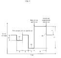
- FIG. 7 shows waveform configuration and shape of drive voltage in the ink jet device 1000 .
- FIG. 8A shows drive waveform of drive voltage used in a verification experiment
- FIG. 8B shows correlation between a proportion in displacement amount X/Y and volume of an ink droplet to be ejected, where X indicates a displacement amount of drive voltage for performing the preliminary drive operation, and Y indicates a displacement amount of drive voltage for performing the main drive operation.
- FIG. 9A shows correlation between flight speed of an ink droplet and angle inequality
- FIG. 9B shows the angle inequality relative to the flight speed and results of a verification experiment on generation of micro droplets.
- FIG. 10A shows correlation between flight speed of an ink droplet and angle inequality
- FIG. 10B shows the angle inequality relative to the flight speed and results of a verification experiment on generation of micro droplets.
- FIG. 11 is a partial cross-sectional view of an organic EL device 100 manufactured by a manufacturing method of an organic EL device relating to an embodiment of the present invention.
- FIG. 12 schematically shows shape of a barrier rib layer of an organic EL display panel as the organic EL device 100 shown in FIG. 11 .
- FIG. 13A to FIG. 13E are cross-sectional views schematically showing part of a manufacturing step of a manufacturing method of the organic EL device 100 .
- FIG. 14A to FIG. 14D are cross-sectional views schematically showing part of the manufacturing step of the manufacturing method of the organic EL device 100 .
- FIG. 15 shows positional relationship between an application target substrate and an ink head units 301 in an application step of the manufacturing method of the organic EL device 100 .
- the volume of the ink droplet to be ejected is set by varying drive voltage of the ink jet device, both of flight speed of the ink droplet, which might influence landing accuracy, and the volume of the ink droplet might sensitively vary with positive correlation coefficients. For this reason, it is desirable to set the volume of the ink droplet in a wide range without varying the drive voltage of the ink jet device as much as possible.
- the inventor and so on earnestly considered reasons why the drive voltage of the ink jet device needs to be set considerably high in order to increase the volume of the ink droplet to a certain value or higher.
- the inventor and so on found that when the drive voltage is applied for ink drop ejection, ununiform pressure is applied to the ink surface in the nozzle, and accordingly high electrical power is necessary to apply considerable pressure in order to eject a necessary ink droplet.
- the present invention was made based on the above expertise.
- an inkjet device comprising: an ink jet head including an ink housing unit that houses therein ink, a pressure application unit that applies pressure to the ink by applying voltage to a piezoelectric element according to a voltage waveform, and a nozzle through which a droplet of the ink is ejected; and an ejection control unit that controls an ejection amount of the droplet of the ink by varying application voltage to be applied to the piezoelectric element, wherein the voltage waveform of the application voltage includes a preliminary vibration waveform part and a main vibration waveform part, the preliminary vibration waveform part is for performing a preliminary drive operation of pushing the ink toward an outer edge of the nozzle to the extent that the droplet of the ink is not ejected through the nozzle, the main vibration waveform part is for performing a main drive operation of ejecting the droplet of the ink through the nozzle after performance of the preliminary drive operation, the ejection control unit performs the preliminary drive operation and the main drive operation according
- the proportion in displacement amount X/Y is set as above because the proportion in displacement amount X/Y of lower than 20% might not clearly exhibit effects of increase in volume of the droplet of the ink to be ejected and the proportion in displacement amount X/Y of higher than 40% might result in ejection of the droplet of the ink through the nozzle.
- variation of drive voltage for ejecting an ink droplet is suppressed, and the displacement amount X of the application voltage for performing the preliminary drive operation is varied.
- the following describes in detail the preliminary drive operation relating to the aspect of the present invention.
- drive voltage is applied to the piezoelectric element in order to expand or shrink the housing unit to apply pressure to ink and generate a propagation wave in ink housed in the ink housing unit.
- an ink droplet is ejected through a nozzle.
- the ink surface has a meniscus shape such that pressure in the ink and surface tension of the ink surface are held in equilibrium. This is considered to cause ununiform energy of the propagation wave on the ink surface.
- the volume of the ink droplet to be ejected is not constant.
- the meniscus shape of the ink surface is a disincentive to obtain an ink droplet having a defined volume.
- the meniscus shape of the ink surface is a disincentive to obtain an ink droplet having a defined volume.
- the preliminary drive operation is performed for pushing the ink housed in the ink housing unit toward the outer edges of the nozzle such that the vertex position of the meniscus shape of the ink surface moves toward the edge of the nozzle.
- the displacement amount X of the application voltage which is for pushing the ink in the preliminary drive operation
- the proportion in displacement amount X/Y of the application voltage is set to equal to or higher than 20%.
- the upper limit of the proportion in displacement amount X/Y is set to 40% because the proportion in displacement amount X/Y set to higher than 40% might cause ejection of ink droplet.
- the displacement amount X of the application voltage in the preliminary drive operation is set to ensure that 20% ⁇ X/Y ⁇ 40% is satisfied.
- the ink housing unit, the pressure application unit, and the nozzle may be each included in plural in the ink jet head, with respect to one or more of the nozzles, the ejection control unit may perform the preliminary drive operation and the main drive operation, and with respect to a remainder of the nozzles, the ejection control unit may not perform the preliminary drive operation.
- the preliminary drive operation is selectively performed with respect to one or more of the nozzles included in the ink jet head.
- the following gives specific description. At present, it is impossible to uniformize volume of an ink droplet between nozzles due to process irregularities between the nozzles, inequality in physical properties of ink such as viscosity and surface tension between the nozzles, and so on. In view of this, the preliminary drive operation is performed in order to reduce the inequality in the volume of the ink droplet between the nozzles.
- the pressure application unit relating to the aspect of the present invention is for example composed of a piezoelectric element having a laminated structure in which a piezoelectric material sandwiched between two electrodes.
- the pressure application unit is provided for each nozzle included in the ink jet head.
- One of the electrodes of the piezoelectric element is attached to a vibration plate, and the pressure application unit shrinks and expands the ink housing unit.
- the members constituting the ink housing unit or the members constituting the pressure application unit are manufactured and processed with accuracy, such that these members each have a predetermined size as designed such as area and thickness of the electrodes, the piezoelectric material, and the vibration plate or diameter of the nozzle.
- the manufacturing irregularities and process irregularities cause inequality in positive pressure to be applied to an ink surface for ejecting an ink droplet, and as a result inequality exists in volume of an ink droplet to be ejected.
- the inequality in volume of the ink droplet is caused by the inevitable manufacturing irregularities and process irregularities, there is a demand for a means for suppressing the inequality as much as possible.
- One example of the means for the inequality is a means for controlling the volume of the ink droplet by varying drive voltage to be applied for ejecting the ink droplet.
- the drive voltage is varied, landing accuracy cannot be controlled. This is because flight speed of an ink droplet to be ejected is varied due to variation of the drive voltage, and the flight speed of the ink droplet to be ejected through the nozzles cannot be uniformly controlled.
- the preliminary drive operation is selectively performed with respect to one or more nozzles included in the ink jet head through which an ink droplet having the defined volume is not ejected due to manufacturing irregularities of the members constituting the ink housing unit or the members constituting the pressure application unit.
- the preliminary drive operation may be set to ensure that a flight speed V of a droplet of the ink to be ejected in the main drive operation satisfies 4 m/s ⁇ V ⁇ 10 m/s.
- the ejected ink droplet In the case where the flight speed of the ink droplet is set low, the ejected ink droplet is deflected from a straight flight course thereof due to air resistance, and this deteriorates landing accuracy.
- the flight speed In the case where the flight speed is set high on the other hand, when the ejected ink droplet (main droplet) flies forwards, a micro droplet of the ink is generated backward, and the micro droplet lands in a position shifted from a predetermined landing position of the main droplet. This also deteriorates landing accuracy. In order to exhibit excellent landing accuracy, it is important to optimize the flight speed of the ink droplet.
- the flight speed increases in accordance with increase of the drive voltage.
- the drive voltage is varied as a means for increasing the volume of the ink droplet to be ejected, not only the flight speed but also the volume of the ink droplet to be ejected increases. This causes a problem that an ink droplet having the defined volume cannot be ejected.
- the displacement amount Y of the application voltage is fixed, it is possible to control the magnitude of the positive pressure to be applied to the ink surface in the main drive operation, by using a variable for the proportion in displacement amount X/Y, which is the proportion of the displacement amount X of the application voltage corresponding to the preliminary vibration waveform part for performing the preliminary drive operation to the displacement amount Y of the application voltage corresponding to the main vibration waveform part for performing the main drive operation.
- the preliminary drive operation is set to ensure that the flight speed V of the ink droplet to be ejected in the main drive operation satisfies 4 m/s ⁇ V ⁇ 10 m/s.
- the flight speed V of the ink droplet falls below 4 m/s, deflection of a flight course of the ejected ink droplet is not tolerable, and this deteriorates landing accuracy.
- the flight speed V of the ink droplet exceeds 10 m/s on the other hand, a considerable number of micro droplets of the ink are generated in the backward of the ejected ink droplet, and this also deteriorates the landing accuracy.
- the voltage waveform of the application voltage may further include a vibration suppression waveform part for performing a vibration suppression operation of suppressing vibration occurring on a surface of the ink due to the main drive operation, and with respect to the nozzle with respect to which the preliminary drive operation is performed, the ejection control unit may perform the vibration suppression operation according to the vibration suppression waveform part.
- vibration remaining due to the main drive operation causes an unexpected ink droplet to separate from the ink surface and adhere near the nozzle.
- the ink droplet adhered near the nozzle is brought into contact with a subsequent ink droplet, and might defect flight direction of the subsequent ink droplet due to surface tension of the adhered ink droplet.
- the vibration suppression operation for suppressing vibration occurring on the ink surface is performed after the main drive operation is performed.
- the voltage waveform of the application voltage includes the vibration suppression waveform part subsequent to the main vibration waveform part.
- the surface of the ink at a start time of the main drive operation after performance of the preliminary drive operation may be positioned more downward than the surface of the ink at a start time of the main drive operation without performance of the preliminary drive operation.
- vibration which remains on the ink surface due to the preliminary drive operation for pushing the ink
- the main drive operation is started at a position where the amplitude toward the inside of the ink housing unit has the maximum magnitude for example, effects can be suppressed that are obtained by pushing the ink toward the outer edge of the nozzle in the preliminary drive operation.
- the remaining vibration resonates with vibration occurring due to the main drive operation, an ink droplet having volume smaller than the defined volume might be ejected.
- the surface of the ink at a start time of the main drive operation after performance of the preliminary drive operation may be positioned more downward than the surface of the ink at a start time of the main drive operation without performance of the preliminary drive operation.
- Vibration remains on the ink surface due to pushing of ink in the preliminary drive operation. Amplitude of the remaining vibration is suppressed by flattening the meniscus shape in the preliminary drive operation.
- the remaining vibration might resonate with vibration occurring due to the main drive operation.
- the main drive operation is started while the amplitude toward the inside of the ink housing unit has the maximum magnitude, the remaining vibration resonates with the vibration occurring due to the main drive operation to a great extent. Since this resonation might cause ejection of an ink droplet having volume smaller than the defined droplet, the effects obtained by performing the preliminary drive operation cannot be sufficiently exhibited.
- the main drive operation is started while the ink surface is positioned further more downward (closer to an outer edge of the nozzle) than the ink surface with no preliminary drive operation.
- the main drive operation is started while the ink surface is positioned further more downward (closer to an outer edge of the nozzle) than the ink surface with no preliminary drive operation.
- the preliminary drive operation should be desirably started while the vertex of the meniscus shape of the ink surface is positioned closer to the outer edge of the nozzle than the vertex of the meniscus shape of the ink surface in static state.
- the ink surface is restored to the meniscus shape.
- the ink surface is not in static state, and vibration remains on the ink surface due to the main drive operation.
- the amplitude is the highest around the vertex of the meniscus shape.
- the remaining vibration resonates with the vibration occurring due to the preliminary drive operation to a great extent. Since this resonation might cause ejection of an ink droplet during the preliminary drive operation, the effects obtained by performing the preliminary drive operation cannot be sufficiently exhibited.
- the preliminary drive operation is started while the vertex of the meniscus shape of the ink surface is positioned closer to the outer edge of the nozzle than the vertex of the meniscus shape of the ink surface in static state.
- Another aspect of the present invention provides a method of manufacturing an organic EL device comprising: forming a first electrode on a substrate; forming one or more functional layers including a light-emitting layer on the first electrode; forming a second electrode on the functional layers, wherein in the forming the functional layers, the functional layers including at least the light-emitting layer are formed by applying ink including material of the functional layer and solvent with use of the ink jet device of any of the above aspects of the present invention, and evaporating and drying the solvent.
- An organic EL display panel has the device configuration in which a plurality of organic EL elements are arranged on a substrate in matrix.
- An organic EL device has the device configuration in which anodes, one or more functional layers including a light-emitting layer, and a cathode are layered on a substrate in this order.
- the light-emitting layer is formed by the inkjet method as follows for example. Ink containing organic material of light-emitting layer is applied by the inkjet method to a plurality of pixel apertures that are partitioned by a barrier rib formed on the substrate. Then, solvent contained in the ink is removed by drying and so on.
- an ink jet technique for layer formation with use of a conventional ink jet device in the case where for example flight speed of an ink droplet relating to landing accuracy is kept without variation of drive voltage to be applied as much as possible, it is impossible to uniformly control volume of an ink droplet to be ejected, and this results in inequality in droplet volume.
- the inequality in volume of an ink droplet makes film thickness to be ununiform between pixels, and as a result electric current does not uniformly flow to the pixels, or electric current collectively flows to a part of a pixel having thin film thickness. This causes inequality or deterioration in light-emitting characteristics and light-emitting lifetime.
- the problem caused by the inequality in volume of an ink droplet to be ejected incurs decrease in manufacturing yield, and therefore urgent solution of this technical problem is desired.
- the functional layers including at least the light-emitting layer are formed by applying ink including material of the functional layer and solvent with use of the ink jet device relating to any of the above aspects of the present invention, and evaporating and drying the solvent.
- FIG. 1 shows the primary configuration of the ink jet device 1000 relating to the present embodiment.
- FIG. 2 is a functional block diagram showing the ink jet device 1000 .
- the ink jet device 1000 includes an ink jet table 20 , a head unit 30 , and a control device 15 .
- the control device 15 includes a CPU 150 , a storage unit 151 (including a large-capacity storage unit such as an HDD), a display unit (display) 153 , and an input unit 152 .
- a control device 15 is a personal computer (PC).
- the storage unit 151 stores therein control programs and so on for driving the ink jet table 20 and the head unit 30 which are connected to the control device 15 .
- the CPU 150 performs predetermined control based on an instruction input by an operator via the input unit 152 and the control programs stored in the storage unit 151 .
- the ink jet device 1000 is illustrated as including the single head unit 30 having a single ink jet head 301 , the configuration of the ink jet device 1000 is not limited to this.
- the ink jet head 301 may be provided in plural.
- the single head unit 30 may have a plurality of ink jet heads 301 .
- the plurality of head units 30 each may have one or more ink jet heads 301 .
- the ink jet table 20 is a so-called gantry work table where a gantry unit (movable frame) is movably disposed along a pair of guiding shafts on a base.
- a gantry unit movable frame
- a specific configuration of the ink jet table 20 is as follows. Columnar stands 201 A, 201 B, 202 A and 202 B are arranged at the four corners of an upper surface of a plate-like base 200 . A fixed stage ST and an ink pan (dish-like container) IP are disposed in an inner region surrounded by the stands 201 A, 201 B, 202 A and 202 B. An application target substrate is placed on the fixed stage ST. Immediately before ink is applied to the application target substrate, the ink is ejected into the ink pan IP to stabilize ejection properties.
- guiding shafts 203 A and 203 B are supported by the stands 201 A and 201 B and the stands 202 A and 202 B, respectively in such a manner that the guiding shafts 203 A and 203 B extend in the longitudinal direction of the base 200 (the Y direction) in parallel with each other.
- the guiding shafts 203 A and 203 B are inserted through linear motor units 204 and 205 , respectively.
- a gantry unit 210 is mounted on the linear motor units 204 and 205 so as to suspend the guiding shafts 203 A and 203 B over the linear motor units 204 and 205 , respectively.
- the gantry unit 210 slides back and forth in the longitudinal direction of the guiding shafts 203 A and 203 B (the Y-axis direction) due to driving of the pair of linear motor units 204 and 205 .
- the gantry unit 210 is provided with a movable member (carriage) 220 that is composed of an L-shaped mount.
- the movable member 220 is provided with a servo motor unit (movable motor) 221 .
- Gears which are not illustrated are attached to the tip of the shaft of the servo motor unit 221 .
- the gears fit into a guiding groove 211 extending in the longitudinal direction of the gantry unit 210 (the X direction).
- a minute rack extending in the longitudinal direction of the gantry unit 210 is disposed inside the guiding groove 211 .
- the gears are engaged with the rack. Accordingly, when the servo motor unit 221 is driven, the movable member 220 moves back and forth with precision in the X-axis direction by a so-called rack and pinion mechanism.
- the movable member 220 is provided with the head unit 30 . Accordingly, it is possible to control the head unit 30 to scan the application target substrate by moving the gantry unit 210 in the longitudinal direction of the guiding shafts 203 A and 203 B while the movable member 220 is fixed to the gantry unit 210 , or by moving the movable member 220 in the longitudinal direction of the gantry unit 210 while the gantry unit 210 is suspended.
- the main scanning direction and the sub scanning direction of the head unit 30 are the column (the Y-axis) direction and the row (the X-axis) direction, respectively.
- the linear motor units 204 and 205 and the servo motor unit 221 are each connected to the control unit 213 such that the control unit 213 directly controls driving of the linear motor units 204 and 205 and the servo motor unit 221 .
- the control unit 213 is connected to the CPU 150 included in the control device 15 .
- the linear motor units 204 and 205 and the servo motor unit 221 are controlled to drive by the CPU 150 , which has read the control programs, via the control unit 213 (see FIG. 2 ).
- the head unit 30 employs a piezoelectric system, and includes the ink jet head 301 and a body 302 .
- the inkjet head 30 is fixed to the movable member 220 via the body 302 .
- the body 302 has built therein a servo motor unit 304 (see FIG. 2 ). Rotation of the servo motor unit 304 adjusts an angle between the longitudinal direction of the ink jet head 301 and the X-axis of the fixed stage ST.
- FIG. 3A is a partially cutaway perspective cross-sectional view showing the outline configuration of the ink jet head 301 .
- FIG. 3B is a partially enlarged cross-sectional view showing the ink jet head 301 taken along a line B-B′ in FIG. 3A .
- the ink jet head 301 includes a nozzle plate 301 i , a housing plate 301 c , and a vibration plate 301 h that are overlaid in this order.
- the nozzle plate 301 i has a plurality of nozzles 3031 through which droplets D are ejected.
- the housing plate 301 c has barrier ribs 301 d that section ink housing units 301 e that are communicated with the respective nozzles 3031 .
- the vibration plate 301 h has joined thereto piezoelectric elements 3010 that are pressure application units serving as driving means corresponding to the respective ink housing units 301 e.
- the housing plate 301 c has, in addition to the barrier ribs 301 d which section the section ink housing units 301 e communicated with the respective nozzles 3031 , passages 301 f and 301 g through which ink is filled in the ink housing units 301 e .
- the passages 301 f and 301 g are each a space resulting from sandwiching the housing plate 301 c , which includes the barrier ribs 301 d , between the nozzle plate 301 i and the vibration plate 301 h .
- the passage 301 g serves as a reservoir in which ink is stored.
- Ink is supplied from an ink tank or the like through a pipe, and is stored in the reservoir through a supply hole 301 h 1 provided in the vibration plate 301 h . Then, the ink is stored in the ink housing units 301 e through the passage 301 f.
- the piezoelectric elements (the pressure application units) 3010 are each composed of a pair of electrodes 3011 and 3012 that sandwich an element body 3013 therebetween.
- the vibration plate 301 h to which the piezoelectric elements 3010 are joined is deformed.
- This increases or decreases volume of the ink housing units 301 e , which are partitioned by the barrier ribs 301 d .
- ink 40 that is filled in the ink housing units 301 e is increased or decreased in pressure, and liquid material is ejected as droplets D through the nozzles 3031 .
- the vibration plate 301 h is restored to the original shape, and the volume of the ink housing units 301 e is restored. As a result, the ink is sucked from the reservoir to the ink housing units 301 e . It is possible to control amount, ejection timing, and so on of the ink to be ejected through the nozzles 3031 , by controlling the drive voltage to be applied to the piezoelectric elements 3010 .
- a region F surrounded by a dashed line in FIG. 3B indicates a cross-section of a region of the ink jet head 301 corresponding to each of the nozzles 3031 .
- the region F is constituted from the ink housing unit 301 e , the barrier ribs 301 d constituting the ink housing unit 301 e , the vibration plate 301 h , the nozzle plate 301 i , the piezoelectric element 3010 , and the nozzle 3031 .
- the number of the nozzles 3031 included in the ink jet heads 301 is plural.
- the present invention is not limited to this configuration at all.
- the ink jet head 301 may for example have one nozzle 3031 corresponding to only the region F.
- the ink jet head 301 has the nozzles 3031 on a surface thereof facing the fixed stage ST.
- the nozzles 3031 are arranged for example in rows in the longitudinal direction of the ink jet head 301 .
- Ink (liquid material) which is supplied to the ink jet head 301 is ejected through the nozzles 3031 as droplets to the application target substrate.
- the ink jet device 1000 includes the ink jet head 301 having a single type of ink housed therein.
- the present invention is not limited to this configuration.
- the ink jet device 1000 may include the plurality of ink jet head units 30 , and the ink jet heads 301 included in the ink jet head units 30 may for example one-to-one correspond to different types of ink such that different types of droplets are ejected through the nozzles 3031 of the ink jet heads 301 to the application target substrate.
- droplet ejection operations of the nozzles 3031 are controlled in accordance with the drive voltage to be applied to the piezoelectric elements 3010 included in the nozzles 3031 .
- An ejection control unit 300 controls the drive voltage to be applied to the piezoelectric elements 3010 , and as a result predetermined ink droplets are ejected through the nozzles 3031 .
- the CPU 150 reads the predetermined control programs from the storage unit 151 , and instructs the ejection control unit 300 to apply defined voltage to the piezoelectric elements 3010 .
- the ejection control unit 300 controls the drive voltage to be applied to the piezoelectric elements 3010 .
- the vibration plate 301 h of the ink housing unit 301 e is deformed by the plate-like piezoelectric elements 3010 which are flexural vibrators.
- the configuration of the vibrators is not limited to this.
- longitudinal vibrators using rod piezoelectric elements may be for example employed.
- the vibration plate 301 h of the ink housing unit 301 e is deformed in a deformation direction of rod piezoelectric elements.
- FIG. 4A illustratively shows the configuration of drive waveform of drive voltage in a conventional ink jet device
- FIG. 4B schematically shows ejection behavior of ink upon application of the drive voltage shown in FIG. 4A
- FIG. 5A illustratively shows the configuration of drive waveform of drive voltage in the ink jet device 1000 relating to the present embodiment
- FIG. 5B schematically shows ejection behavior of ink upon application of the drive voltage shown in FIG. 5A
- FIG. 4B and FIG. 5B each show only the vicinity of the nozzle 3031 extracted from FIG. 3B .
- the drive waveform of the drive voltage shown in FIG. 4A includes a main vibration waveform part 62 and a vibration suppression waveform part 63 .
- the main vibration waveform part 62 is a waveform part for performing a main drive operation by a so-called pull ejection according to which ink droplet is ejected by first increasing the volume of the ink housing unit to expand the ink housing unit, and then decreasing the volume of the ink housing unit to shrink the ink housing unit.
- the vibration suppression waveform part 63 is a waveform part for performing a vibration suppression operation to suppress vibration that remains on an ink surface due to the main drive operation.
- the ink 40 is located inside the ink housing units 301 e while the ink surface is distant from the outer edge of the nozzle 3031 (section (i) in FIG. 4B ). Accordingly, when the drive voltage corresponding to the main vibration waveform part 62 is applied, ununiform positive pressure is applied to the ink surface. This might result in that a droplet having a smaller volume than the defined volume is ejected, or that such a droplet is ejected in various directions (section (ii) in FIG. 4B ). Also, since ejection of a droplet having the defined volume is impossible, excessive drive voltage might need to be applied in order to increase the volume of the droplet.
- the ink surface at a time immediately before ejection has a meniscus shape that is curved toward inside the ink housing unit 301 e as shown in section (i) in FIG. 4B . Accordingly, the positive pressure applied to the ink surface is ununiform, and amplitude is the highest around the vertex of the meniscus shape. As a result, a droplet D having a smaller volume than the defined volume is ejected, or the droplet D is ejected in the various directions (section (ii) in FIG. 4B ). Therefore, since ejection of the droplet having the defined volume is impossible, excessive drive voltage might need to be applied in order to increase the volume of the droplet D.
- the drive waveform of the drive voltage shown in FIG. 5A includes a preliminary vibration waveform part 61 , a main vibration waveform part 62 , and a vibration suppression waveform part 63 .
- the preliminary vibration waveform part 61 is a waveform part for performing a preliminary drive operation by first increasing the volume of the ink housing unit 301 e to expand the ink housing unit 301 e , and then decreasing the volume of the ink housing unit 301 e to shrink the ink housing unit 301 e .
- the main vibration waveform part 62 and the vibration suppression waveform part 63 are the same as those shown in FIG. 4A .
- the ink 40 is pushed toward the outer edges of the nozzles 3031 , and as a result the ink 40 is changed from the state shown in section (i) in FIG. 5B to the state shown in section (ii) in FIG. 5B . Accordingly, when drive voltage corresponding to the main vibration waveform part 62 is applied, positive pressure applied to the ink surface is uniform, and this increases volume of a droplet of the ink 40 to be ejected. Also, as the volume of the droplet of the ink 40 to be ejected increases, motion energy of the droplet increases.
- the subsequent droplet is less influenced by surface tension, and is ejected with high straightness. This prevents the droplet from being ejected in a bent direction (section (iii) in FIG. 5B ).
- the preliminary vibration waveform part 61 is a waveform part for performing the preliminary drive operation to flatten the meniscus shape by pushing the ink.
- the ink surface has a meniscus shape that is curved toward inside the ink housing unit 301 e as shown in section (i) in FIG. 5B .
- the meniscus shape of the ink surface is flattened through the preliminary drive operation (section (ii) in FIG. 5B ).
- the drive voltage corresponding to the main vibration waveform part 62 is applied, the ink surface at a time immediately before ejection has the meniscus shape that is flattened as described above. Accordingly, the positive pressure applied to the ink surface is uniform, and the amplitude around the vertex of the meniscus shape is smaller than in the case where the meniscus shape is not flattened. This increases the volume of the droplet to be ejected.
- the ink jet device 1000 relating to the present embodiment includes the single ink jet head 301 having the plurality of nozzles 3031 .
- the drive voltage corresponding to the drive waveform shown in FIG. 5A is applied with respect to at least one of the nozzles 3031 .
- the drive waveform includes the preliminary vibration waveform part, the main vibration waveform part, and the vibration suppression waveform part. Since the drive voltage corresponding to the preliminary vibration waveform part, which is independent from the drive voltage corresponding to the main vibration waveform part, is applied prior to the drive voltage corresponding to the main vibration waveform part, it is possible to perform wide-range control on the volume of the droplet to be ejected.
- the preliminary drive operation is performed with respect to the nozzle 3031 through which the ink having the defined volume is not ejected.
- the nozzle 3031 to be targeted is determined in accordance with manufacturing irregularities of the components constituting the ink housing unit 301 e such as the vibration plate 301 h and the nozzle 3031 , the components constituting the pressure application units 3010 , and so on. Specifically, suppose a case where inequality exists between the nozzles 3031 in volume of an ink droplet to be ejected due to the manufacturing irregularities. When the largest volume of an ink droplet among ink droplets having unequal volumes falls within a defined droplet volume range for example, the largest volume is determined as a reference value.
- the drive voltage corresponding to the preliminary vibration waveform part is applied to the respective pressure application units corresponding to the remaining nozzles 3031 to perform the preliminary drive operation such that the volume of the ink droplet in the remaining nozzles 3031 are equal to the largest volume determined as the reference value. Also, when a defined ink droplet volume falls within a range of unequal volumes of ink droplets, drive voltage to be applied for ejecting the defined volume droplet (drive voltage corresponding to the main vibration waveform part) is determined as a reference value.
- drive voltage including drive voltage corresponding to the main vibration waveform part, which is increased or decreased from the reference value by some volts, and drive voltage corresponding to the preliminary vibration waveform part is applied to the respective pressure application units corresponding to the remaining nozzles 3031 to perform the preliminary drive operation.
- the drive voltage having the waveform configuration including the preliminary vibration waveform part and varying the displacement amount of the drive voltage corresponding to the preliminary vibration waveform part it is possible to obtain droplet volume in a wide range only with variation of drive voltage corresponding to the main vibration waveform part in a minute range of some volts (see FIG. 8B shown later). For this reason, the respective displacement amounts of application drive voltages corresponding to the preliminary vibration waveform part and the main vibration waveform part should be appropriately adjusted depending on the status of inequality in droplet volume.
- the ink jet device 1000 relating to the present embodiment includes the single ink jet head 301 .
- drive voltage which has the drive waveform including the preliminary vibration waveform part, the main vibration waveform part, and the vibration suppression waveform part, may be applied with respect to at least one of the ink jet heads or one of the nozzles of the at least one ink jet head.
- the drive voltage corresponding to the drive waveform including the main vibration waveform part and the vibration suppression waveform part exemplified in FIG. 4A may be applied with respect to the remainder of the ink jet heads or nozzles, without performance of the preliminary drive operation.
- the drive voltage corresponding to the main vibration waveform part is applied for performing the main drive operation by the pull ejection method.
- the main drive operation may be performed by the push ejection method for shrinking the ink housing unit 301 e without being expanded once, and the drive voltage corresponding to the main vibration waveform part may be applied as such.
- drive waveform of the drive voltage is as exemplified in FIG. 6A .
- the drive waveform of the drive voltage includes the vibration suppression waveform part.
- the drive waveform of the drive voltage may include only the preliminary vibration waveform part and the main vibration waveform part such as exemplified in FIG. 6B .
- the drive voltage corresponding to the preliminary vibration waveform part is applied for performing the preliminary drive operation by the pull ejection method.
- the drive voltage corresponding to the preliminary vibration waveform part may be applied by the push ejection method for shrinking the ink housing unit 301 e without being expanded once.
- drive waveform of the drive voltage is as exemplified in FIG. 6C .
- the waveform configuration of the drive voltage is not limited to that shown in the present embodiment, and only needs to have the waveform configuration including the preliminary vibration waveform part for performing the preliminary drive operation to pushing ink toward the outer edge of the nozzle and the main vibration waveform part subsequent to the preliminary vibration waveform part for ejecting an ink droplet.
- FIG. 7 shows drive waveform of drive voltage used in the present embodiment.
- the preliminary vibration waveform part 61 , the main vibration waveform part 62 , and the vibration suppression waveform part 63 have waveform widths A, B, and C, respectively, and voltages applied for performing the preliminary drive operation, the main drive operation, and the vibration suppression operation have displacement amounts X, Y, and Z, respectively.
- the following describes the displacement amount and the drive waveform width with respect to each of the preliminary vibration waveform part, the main vibration waveform part, and the vibration suppression waveform part.
- the lower limit of the displacement amount X of application drive voltage corresponding to the preliminary vibration waveform part should be a value necessary for pushing ink to the extent that an ink droplet having the defined volume can be ejected in the main drive operation.
- the upper limit of the displacement amount X should be a value to the extent that an ink droplet is not ejected in the preliminary drive operation.
- a preferable range of the displacement amount X of the application drive voltage is set in relation to the displacement amount Y of the application drive voltage to ensure that 20% ⁇ X/Y ⁇ 40% is satisfied.
- the displacement amount Y of application drive voltage generally falls within a range of 10V to 50V.
- the lower limit of the displacement amount X of the application drive voltage should be a value that allows to flatten the meniscus shape of the ink surface to the extent that an ink droplet having the defined volume is ejected in the main drive operation. Accordingly, a preferable range of the displacement amount X is set to ensure that 20% ⁇ X/Y is satisfied. The upper limit of the displacement amount X is set to ensure that 20% ⁇ X/Y ⁇ 40% is satisfied.
- the waveform width A of the preliminary vibration waveform part is set such that vibration that remains on the ink surface due to the main drive operation or vibration that occurs due to application of drive voltage corresponding to the preliminary vibration waveform part for expanding the ink housing unit does not resonate with vibration that occurs due to application of drive voltage for shrinking the ink housing unit 301 e in the preliminary drive operation.
- the waveform width A is for example set to T/2 that is half a period T of the helmholtz resonance frequency in the ink housing unit 301 e.
- the drive voltage corresponding to the preliminary vibration waveform part is applied for performing the preliminary drive operation by the pull ejection method.
- the drive voltage corresponding to the preliminary vibration waveform part may be applied for performing the preliminary drive operation by the push ejection method as shown in FIG. 6C .
- the values of the displacement amount and waveform width of the drive voltage may be used that are the same as those in the present embodiment.
- the preliminary drive operation by the pull ejection method is advantageous in that an application period necessary for one cycle of waveform is reduced. This is because the preliminary drive operation by the pull ejection method allows to push ink at a low drive voltage compared with the preliminary drive operation by the push ejection method, thereby reducing the displacement amount of application drive voltage.
- the displacement amount Y of the application drive voltage corresponding to the main vibration waveform part is set in accordance with the physical properties of the used ink such that ink droplets are ejected in the main drive operation.
- the displacement amount Y of the application drive voltage is suppressed low compared with the case where the preliminary drive operation is not performed, and driving at this low drive voltage allows to reduce an application period necessary for one cycle of waveform.
- the waveform width C of the main vibration waveform part is set such that vibration that remains on the ink surface due to application of the drive voltage corresponding to the preliminary vibration waveform part does not resonate with vibration that occurs due to the main drive operation.
- the waveform width C is for example set to T/2 that is half the period T of the helmholtz resonance frequency in the ink housing unit.
- the drive voltage corresponding to the main vibration waveform part is applied for performing the main drive operation by the pull ejection method.
- the drive voltage corresponding to the main vibration waveform part may be applied for performing the main drive operation by the push ejection method as shown in FIG. 6A .
- the values of the displacement amount and waveform width of the drive voltage may be used that are the same as those in the present embodiment.
- the main drive operation by the pull ejection method is advantageous in that an application period necessary for one cycle of waveform is reduced. This is because the main drive operation by the pull ejection method allows to eject ink droplets at a low drive voltage compared with the main drive operation by the push ejection method, thereby reducing the displacement amount of application drive voltage.
- Drive voltage corresponding to the vibration suppression waveform part is opposite to the drive voltage corresponding to the main vibration waveform part, and is applied for suppressing amplitude of vibration remaining on the ink surface due to the main drive operation.
- a preferable range of the displacement amount Z of the application drive voltage corresponding to the vibration suppression waveform part is set to ensure that 30% ⁇ Z/Y is satisfied. This preferably suppresses the amplitude of vibration that remains on the ink surface due to the main drive operation.
- the upper limit of the displacement amount Z is not particularly limited. However, since increase in displacement amount of application drive voltage increases an application period necessary for one cycle of waveform, the upper limit of the displacement amount Z should be set such that Z/Y ⁇ 60% is satisfied.
- the waveform configuration of drive voltage in the present embodiment shown in FIG. 7 which includes the preliminary vibration waveform part 61 , the main vibration waveform part 62 , and the vibration suppression waveform part 63 , relationship X/Y+Z/Y ⁇ 100% needs to be satisfied. Accordingly, the upper limit of the proportion in displacement amount Z/Y is also defined in accordance with the proportion in displacement amount X/Y relating to the application drive voltage which is necessary for performing the preliminary drive operation.
- the waveform width D of the vibration suppression waveform part is set such that vibration that occurs due to the vibration suppression operation does not resonate with vibration that remains on the ink surface due to application of drive voltage corresponding to the main vibration waveform part, and furthermore such that amplitude of the remaining vibration is attenuated as much as possible.
- the waveform width D is for example set to T/2 that is half the period T of the helmholtz resonance frequency in the ink housing unit.
- the waveform configuration of application drive voltage includes the vibration suppression waveform part.
- the vibration suppression waveform part is not essential.
- the drive voltage corresponding to the vibration suppression waveform part is applied as shown in FIG. 7 such that there is no displacement amount between the drive voltage corresponding to the vibration suppression waveform part and the drive voltage corresponding to the preliminary vibration waveform part. In other words, when the vibration suppression operation is started, the drive voltage is immediately decreased to the drive voltage at the start time of the preliminary drive operation.
- the drive voltage corresponding to the vibration suppression waveform part is not limited to being applied in this way. Alternatively, the drive voltage corresponding to the vibration suppression waveform part may be applied such as shown in FIG.
- the drive voltage corresponding to the vibration suppression waveform part may be applied such that the vibration suppression waveform part have a rectangle shape by performing the vibration suppression operation at the displacement amount Z having a larger value than the displacement amount Z shown in FIG. 7 , keeping the drive voltage for a certain period, and then applying the drive voltage corresponding to the vibration suppression waveform part until immediately before application of the drive voltage corresponding to the preliminary vibration waveform part.
- the wave configuration of the application drive voltage in the present embodiment includes the preliminary vibration waveform part, which is independent from the main vibration waveform part. Accordingly, there is a relay period B between the application period of the drive voltage corresponding to the preliminary vibration waveform part and the application period of the drive voltage corresponding to the main vibration waveform part.
- the relay period B is set such that vibration that remains on the ink surface due to application of the drive voltage corresponding to the preliminary vibration waveform part does not resonate with vibration that occurs due to application of the drive voltage corresponding to the main vibration waveform part for expanding the ink housing unit.
- the relay period B is for example set to T/2 that is half the period T of the helmholtz resonance frequency in the ink housing unit.
- the relay period should be set such that vibration that remains on the ink surface due to previous or immediately previous application of drive voltage does not resonate with vibration that occurs on the ink surface due to subsequent application of drive voltage.
- the relay period should be preferably for example set to T/2 that is half the period T of the helmholtz resonance frequency in the ink housing unit.
- the present inventor found the expertise that volume of an ink droplet to be ejected is increased by pushing ink toward the outer edge of the nozzle to the extent that the ink droplet is not ejected, more specifically by flattening the meniscus shape of the ink surface, prior to the drive operation for ejecting the ink droplet. Then, the present inventor reached a conclusion that, by controlling application drive voltage for pushing the ink toward the outer edge of the nozzle to the extent that the ink droplet is not ejected, it is possible to perform wide-range control on the volume of the ink droplet without varying the application drive voltage as much as possible. The following describes results of a verification experiment that lead to the above conclusion with reference to FIG. 8A and FIG. 8B .
- FIG. 8A shows drive waveform of drive voltage used in the verification experiment.
- FIG. 8B shows correlation between the proportion in displacement amount X/Y and volume of an ink droplet to be ejected, where X indicates the displacement amount of the drive voltage for performing the preliminary drive operation, and Y indicates the displacement amount of the drive voltage for performing the main drive operation.
- driving voltage having the same waveform configuration as that shown in FIG. 7 was applied, which includes the preliminary vibration waveform part for performing the preliminary drive operation, the main vibration waveform part for performing the main drive operation, and the vibration suppression waveform part for performing the vibration suppression operation.
- an ink jet head which includes an ink housing unit having a nozzle with diameter of 20 ⁇ m, and the cycle T of the Helmholtz resonance frequency in the ink housing unit was 6 ⁇ s.
- Waveform width of each of the waveform parts and relay time between the application period of the drive voltage corresponding to the preliminary vibration waveform part and the application period of the drive voltage corresponding to the main vibration waveform part were set in accordance with the cycle T.
- the displacement amount Y of the drive voltage was set so as to be a value (black rectangle in the figure) greater by 2 V than a reference voltage value (black circle in the figure) and a value (black triangle in the figure) smaller by 2 V than the reference voltage value.
- Frequency of the drive voltage was set to 1 kHz so as not to be influenced by repetition of ink drop ejection.
- Volume of an ink droplet to be ejected shown in FIG. 8B was measured by spot observation through magnification photographing using a microscope provided with a high-speed camera.
- the volume of the ink droplet was obtained by calculating area of a region having a value darker than an appropriate threshold value from a lateral image of a spherical droplet, and converting the calculated area into a three-dimensional volume.
- the threshold value is manually adjusted so as to be equivalent to the outer periphery of the droplet with reference to the lateral image.
- the inks used in the verification experiment have solute (organic material) concentration of 5% by weight or lower, viscosity of 30 mPa ⁇ s or lower, and surface tension of 20 mN/m to 70 mN/m.
- the ink used in the verification experiment in FIG. 8B contains CHB (cyclohexylbenzene) as solvent, and contains F8-F6 (copolymer of F8 (poly dioctylfluorene) and F6 (poly dihexylfluorene)) as solute having weight-average molecular weight of 200000 and concentration of 0.6% by weight.
- the ink has viscosity of 9.8 mP ⁇ s, surface tension of 34 mN/m, and ligament length of 162 ⁇ m that is length of a linear trail extending backward from part of the ejected ink droplet.
- the ligament length was measured by spot observation of the flying ink droplet through magnification photographing using a microscope provided with a high-speed camera. The viscosity and the surface tension were measured under the conditions of 20 degrees C. with use of the rheometer AR-G2 manufactured by TA Instruments, Inc.
- the volume of the ink droplet to be ejected increased in accordance with increase of the proportion in displacement amount X/Y.
- a trend was observed that an increase curve of the volume of the ink droplet relative to the displacement amount X/Y shows that when the proportion in displacement amount X/Y is 20% or higher, an increase rate of the volume of the ink droplet increases.
- the range of the volume of the ink droplet increases relative to the proportion in displacement amount X/Y. Specifically, the range of the volume of the ink droplet of approximately 2 at the proportion in displacement amount X/Y of 0% increases to approximately 3 at the proportion in displacement amount X/Y of 40%.
- the verification experiment demonstrated that volume of an ink droplet to be ejected effectively increases by setting the proportion in displacement amount X/Y to 20% or higher.
- the proportion in displacement amount X/Y exceeded 40%, a phenomenon was observed that application of the drive voltage corresponding to the preliminary vibration waveform part causes an ink droplet to be ejected through the nozzle.
- the displacement amount X/Y should be set to a range of 20% to 40%.
- the verification experiment demonstrated that it is possible to perform wide-range control on the volume of the ink droplet to be ejected, by suppressing variation of drive voltage, minutely varying the drive voltage Y, and using the proportion in displacement amount X/Y as a variable.
- Flight speed of an ink droplet relates to landing accuracy of the ink droplet.
- the displacement amount Y was set to each of the reference voltage value, a value greater than the reference voltage value by 2 V, and a value smaller than the reference voltage value by 2 V.
- the proportion in displacement amount X/Y was varied within the range of 20% to 40% and flight speed of an ink droplet was measured with respect to each of these values of the displacement amount Y.
- Verification experiment was made on angle inequality in ejection direction relating to a landing position and whether a micro droplet (mist) is generated backward in the ejection direction. The angle inequality is a preferable parameter for judging the landing accuracy. Results of the verification experiment are shown in FIG. 9A , FIG. 9B , FIG. 10A , and FIG. 10B .
- the conditions for the verification experiment which include the type of ink, the configuration of the ink jet head, the drive voltage, and so on, were the same as those described in the section (Effects of Increase in Volume of Ink Droplet to be ejected owing to Preliminary Drive Operation).
- the angle inequality and the flight speed were measured by spot observation of the flying ink droplet through magnification photographing using a microscope provided with a high-speed camera.
- the angle inequality was obtained by measuring a value from observation data where angle of 0 is defined in the case where an ink droplet ejected through the nozzle travels straight toward an application target substrate.
- the flight speed was obtained by measuring a flight distance per constant period from observation data.
- the ink used in the verification experiment in FIG. 9A and FIG. 9B is the same as that shown in FIG. 8B .
- the ink used in the verification experiment in FIG. 10A and FIG. 10B is the same as that shown in FIG. 8B in terms of solute, solvent, and solute weight-average molecular weight, and has solute concentration of 0.3% by weight, viscosity of 6.1 mP ⁇ s, surface tension of 34 mN/m, and ligament length of 106 ⁇ m.
- FIG. 9A and FIG. 10A the angle inequality of the ink droplet to be ejected rapidly increased in accordance with decrease in flight speed of the ink droplet to be ejected.
- a standard value ⁇ excellent landing accuracy is realized with few shift width in landing position.
- FIG. 9B and FIG. 10B are each a table showing whether angle inequality relative to each flight speed is satisfactory or unsatisfactory for the standards. As shown in these tables, when the flight speed is equal to or higher than 4 m/s, the angle inequality is satisfactory for the standards, and accordingly excellent landing accuracy is realized.
- FIG. 9A and FIG. 10A the angle inequality of the ink droplet to be ejected decreased in accordance with increase in flight speed of the ink droplet. This ensures straight flight of the ink droplets.
- FIG. 9B and FIG. 10B are each a table showing whether micro droplet is generated. As shown in these tables, when the flight speed is 10 m/s or lower, generation of micro droplets is suppressed, and accordingly excellent landing accuracy is realized.
- FIG. 11 is a partial cross-sectional view of an organic EL device 100 manufactured by the manufacturing method of an organic EL device relating to the present embodiment.
- the organic EL device 100 shown in FIG. 11 is illustrated as an organic EL display panel including a plurality of organic EL elements 115 , this is just an example.
- the organic EL device 100 may include a single organic EL element.
- the organic EL device 100 is of a so-called top emission type, and has a display surface on the upper side in the figure.
- a TFT (thin film transistor) layer 102 , feed electrodes 103 , and a planarizing film 104 are layered on a substrate body 101 in this order.
- a substrate 105 is constituted from the substrate body 101 , the TFT layer 102 , the feed electrodes 103 , and the planarizing film 104 .
- Pixel electrodes 106 and a hole injection layer 109 are layered on the substrate 105 in this order.
- a barrier rib layer 107 is formed on the hole injection layer 109 . Each adjacent two portions of the barrier rib layer 107 have an aperture 117 therebetween, in which a light-emitting layer 111 is to be formed.
- a hole transport layer 110 and the light-emitting layer 111 are layered in the aperture 117 in this order.
- An electron transport layer 112 , an electron injection layer 113 , and a common electrode 114 are layered in this order on each of the light-emitting layers 111 and the barrier rib layer 107 .
- the hole injection layer 109 , the hole transport layers 110 , the light-emitting layers 111 , the electron transport layer 112 , and the electron injection layer 113 are each equivalent to the functional layer of the present invention.
- the pixel electrodes 106 and the common electrode 114 are equivalent to the first electrode and the second electrode of the present invention, respectively.
- the substrate body 101 is a back substrate of the organic EL device 100 , and has a surface on which the TFT layer 102 including TFTs is formed to drive the organic EL device 100 by an active matrix method.
- the TFT layer 102 has the feed electrodes 103 formed thereon for feeding external electrical power to the TFTs.
- the planarizing film 104 is provided for planarizing surface level difference caused by provision of the TFT layer 102 and the feed electrodes 103 .
- the planarizing film 104 is made of organic material having excellent electrically-insulating properties.
- the substrate 105 which is constituted from the substrate body 101 , the TFT layer 102 , the feed electrodes 103 , and the planarizing film 104 , is equivalent to the substrate of the present invention.
- Contact holes 118 are provided for electrically connecting the feed electrodes 103 with the pixel electrodes 106 , and are through-holes in the planarizing film 104 .
- the contact holes 118 are each formed so as to position between each adjacent two apertures 117 which are arranged in the Y-direction, and are covered with the barrier rib layer 107 . If the contact holes 118 are not covered with the barrier rib layer 107 , the light-emitting layers 111 are not planar due to the existence of the contact holes 118 , and this causes unevenness in light emission and so on. In order to avoid such unevenness in light emission and so on, the contact holes 118 have the above configuration.
- the pixel electrodes 106 are anodes, and are each formed for each light-emitting layer 111 which is formed in the aperture 117 . Since the organic EL device 100 is of the top emission type, the pixel electrodes 106 are made of highly light-reflective material. The pixel electrodes 106 are equivalent to the first electrodes of the present invention.
- the hole injection layer 109 is provided in order to promote injection of holes from the pixel electrodes 106 to the light-emitting layers 111 .
- the barrier rib layer 107 has a function of, when the light-emitting layers 111 are formed, preventing mixing of inks (liquid materials), which contain materials of light-emitting layers and solvent, between red (R), green (G), and blue (B) colors.
- the barrier rib layer 107 is provided so as to cover the above of the contact holes 118 , and has trapezoidal cross-sections along an X-Z plane or a Y-Z plane.
- FIG. 12 schematically shows the shape of the barrier rib layer 107 when the organic EL display panel as the organic EL device 100 is seen from the side of the display surface, where the hole transport layer 110 , the light-emitting layers 111 , the electron transport layer 112 , the electron injection layer 113 , and the common electrode 114 are omitted for convenience of the description. Note that the partial cross-sectional view in FIG. 11 is taken along a line A-A′ in FIG. 12 .
- the organic EL display panel 100 has the configuration in which a plurality of organic EL elements 115 R of the R color, a plurality of organic EL elements 115 G of the G color, and a plurality of organic EL elements 115 B of the B color are arranged in the X-Y direction (in matrix).
- the organic EL elements 115 R, 115 G, and 115 B are each a subpixel, and a combination of three subpixels of the organic EL elements 115 R, 115 G, and 115 B corresponds to one pixel.
- the apertures 117 which are formed in the barrier rib layer 107 , are arranged in the X-Y direction each so as to correspond to one of the organic EL elements 115 R, 115 G, and 115 B.
- the apertures 117 are each a region where the light-emitting layer 111 is to be formed.
- the arrangement and shape of the light-emitting layers 111 are defined in accordance with the arrangement and shape of the apertures 117 .
- the apertures 117 are each a rectangle having a long side in the Y direction. Specifically, the apertures 117 for example each have a side of approximately 30 ⁇ m to 130 ⁇ m in the X direction (the column direction) and a side of approximately 150 ⁇ m to 600 ⁇ m in the Y direction (the row direction).
- the apertures 117 are each specifically one of apertures 117 R, 117 G, and 117 B that respectively correspond to the R, G, and B colors.
- the respective light-emitting layers 111 of the R, G, and B colors are respectively formed in the apertures 117 R, 117 G, and 117 B.
- the apertures 117 R, 117 G, and 117 B respectively correspond to the organic EL elements 115 R, 115 G, and 115 B.
- the apertures 117 are arranged in rows for each of the R, G, and B colors. The apertures 117 which belong to the same row are for the same color.
- the contact holes 118 are each positioned between each adjacent two of the apertures 117 which are arranged in the Y direction, and in the lower part in the barrier rib layer 107 .
- the pixel electrodes 106 are each formed for each of the light-emitting layers 111 formed in the apertures 117 . This means that the pixel electrodes 106 are each provided for each subpixel.
- the hole transport layer 110 has a function of transporting holes injected by the pixel electrodes 106 to the light-emitting layers 111 .
- the light-emitting layers 111 emit light through recombination of carriers, and each include light-emitting material corresponding to one of the R, G, and B colors.
- the respective light-emitting layers 111 including light-emitting materials of the R, G, and B colors are respectively formed in the apertures 117 R, 117 G, and 117 B.
- the electron transport layer 112 has a function of transporting electrons injected by the common electrode 114 to the light-emitting layers 111 .
- the electron injection layer 113 has a function of promoting injection of holes from the common electrode 114 to the light emitting layers 111 .
- the common electrode 114 is a cathode, and is equivalent to the second electrode of the present invention. Since the organic EL display panel 100 is of the top emission type, the common electrode 114 is made of light-transmissive material.
- a sealing layer is provided for suppressing deterioration of the light emitting layers 111 due to exposure to moisture, air, and so on. Since the organic EL display panel 100 is of the top emission type, the sealing layer is made of light-transmissive material such as SiN (silicon nitride) and SiON (silicon oxynitride).
- an ITO (indium tin oxide) layer or an IZO (indium zinc oxide) layer may be provided between each of the pixel electrodes 106 and the hole injection layer 109 for improving bondability therebetween. Furthermore, all the light-emitting layers 111 formed in the apertures 117 may be of the same color.
- the substrate body 101 electrically-insulating material such as non-alkali glass, soda glass, nonfluorescent glass, phosphate glass, borate glass, quartz, acrylic resin, styrenic resin, polycarbonate resin, epoxy resin, polyethylene, polyester, silicone resin, and alumina
- the planarizing film 104 polyimide resin or acrylic resin
- the pixel electrodes 106 Ag (silver), Al (aluminum), alloy of silver, palladium, and copper, alloy of silver, rubidium, and gold, MoCr (alloy of molybdenum and chrome), or NiCr (alloy of nickel and chrome)
- the barrier rib layer 107 acrylic resin, polyimide resin, or novolac-type phenolic resin
- the hole injection layer 109 metal oxide such as MoOx (molybdenum oxide), WOx (tungsten oxide), and MoxWyOz (molybdenum tungsten oxide), metal nitride, or metal oxynitride
- the hole transport layer 110 triazole derivative, oxadiazole derivative, imidazole derivative, polyarylalkane derivative, pyrazoline derivative and pyrazolone derivative, phenylenediamine derivative, arylamine derivative, amino-substituted chalcone derivative, oxazole derivative, styrylanthracene derivative, fluorenone derivative, hydrazone derivative, stilbene derivative, porphyrin compound, aromatic tertiary amine compound, styrylamine compound, butadiene compound, polystyrene derivative, hydrazone derivative, triphenylmethane derivative, or tetraphenylbenzene derivative (all disclosed in Japanese Patent Application Publication No. H5-163488)
- the light-emitting layers 111 F8-F6 (copolymer of F8 (poly dioctylfluorene) and F6 (poly dihexylfluorene)), or fluorescent material disclosed in Japanese Patent Application Publication No.
- H5-163488 such as oxinoid compound, perylene compound, coumarin compound, azacoumarin compound, oxazole compound, oxadiazole compound, perinone compound, pyrrolo-pyrrole compound, naphthalene compound, anthracene compound, fluorene compound, fluoranthene compound, tetracene compound, pyrene compound, coronene compound, quinolone compound and azaquinolone compound, pyrazoline derivative and pyrazolone derivative, rhodamine compound, chrysene compound, phenanthrene compound, cyclopentadiene compound, stilbene compound, diphenylquinone compound, styryl compound, butadiene compound, dicyanomethylene pyran compound, dicyanomethylene thiopyran compound, fluorescein compound, pyrylium compound, thiapyrylium compound, selenapyrylium compound, telluropyrylium compound
- the electron transport layer 112 barium, phthalocyanine, or lithium fluoride
- the electron injection layer 113 nitro-substituted fluorenone derivative, thiopyran dioxide derivative, diphenylquinone derivative, perylene tetracarboxyl derivative, anthraquinodimethane derivative, fluoronylidene methane derivative, anthrone derivative, oxadiazole derivative, perinone derivative, or quinoline complex derivative (all disclosed in Japanese Patent Application Publication No. H5-163488)
- the common electrode 114 ITO or IZO
- a substrate 101 is prepared on which a TFT layer 102 and feed electrodes 103 are formed ( FIG. 13A ).
- a planarizing film 104 having thickness of approximately 4 ⁇ m is formed on the TFT layer 102 and the feed electrodes 103 using organic material having excellent electrically-insulating properties by a photoresist method.
- contact holes 118 are each formed in accordance with the position between each two apertures 117 which are adjacent to each other in the Y direction ( FIG. 13B ).
- the planarizing film 104 and the contact holes 118 can be formed simultaneously.
- the contact holes 118 are of course not limited to being formed by this method.
- the contact holes 118 may be for example formed by, after uniformly forming the planarizing film 104 , removing portions of the planarizing film 104 at predetermined positions. This completes a step of forming the substrate 105 .
- a pixel electrode 106 is formed on the substrate 105 for each subpixel by a vacuum deposition method or a sputtering method, so as to be electrically connected to a corresponding one of the feed electrodes 103 .
- the pixel electrode 106 has thickness of approximately 150 nm and is made of metal material. This step of forming the pixel electrodes 106 on the substrate 105 is equivalent to the forming the first electrode of the present invention.
- a hole injection layer 109 is formed by a reactive sputtering method ( FIG. 13C ).
- a barrier rib layer 107 is formed by a photolithography method. Firstly, material including photosensitive resist in paste form is prepared as material of barrier rib layer. The material of barrier rib layer is uniformly applied on the hole injection layer 109 . A mask shaped into a pattern of the apertures 117 shown in FIG. 12 is overlaid on the applied material of barrier rib layer. Next, the material of barrier rib layer on which the mask is overlaid is exposed to light. As a result, a pattern of barrier rib layer is formed. Subsequently, excess part of the material of barrier rib layer is washed off with an aqueous or non-aqueous etchant (developer). This completes patterning of the material of barrier rib layer. In this way, the apertures 117 in which light-emitting layers 111 are to be formed are defined, and the barrier rib layer 107 having repellency at least on a surface thereof is complete ( FIG. 13D ).
- the surface of the barrier rib layer 107 may be treated with predetermined alkaline solution, water, or organic solvent, or by plasma treatment, in order to adjust the angle of contact between the barrier rib layer 107 and ink for hole transport layer and between the barrier rib layer 107 and ink for organic light-emitting layers to be applied to the apertures 117 in a subsequent step, or to provide the surface of the barrier rib layer 107 with repellency.
- the ink for hole transport layer is prepared by mixing material of a hole transport layer 110 and solvent at a predetermined ratio.
- the ink for hole transport layer is supplied to the ink jet heads 301 , and droplets D as the ink for hole transport layer are ejected through the nozzles 3031 (see FIG. 3 ) corresponding to the apertures 117 in the application step ( FIG. 13E ).
- the solvent contained in the ink is evaporated and dried, and is further heated and baked as necessary.
- the hole transport layer 110 is formed ( FIG. 14A ).
- the ink for organic light-emitting layers is prepared by mixing organic material of the light-emitting layers 111 and solvent at a predetermined ratio.
- the ink for organic light-emitting layers is supplied to the ink jet heads 301 , and droplets D as the ink for organic light-emitting layers are ejected through the nozzles 3031 corresponding to the apertures 117 in the application step ( FIG. 14B ).
- the solvent contained in the ink is evaporated and dried, and is further heated and baked as necessary.
- the light-emitting layers 111 are formed ( FIG. 14C ).
- material of an electron transport layer 112 is formed on surfaces of the light-emitting layers 111 by the vacuum deposition method. As a result, the electron transport layer 112 is formed. Subsequently, material of an electron injection layer 113 is formed by a vapor deposition method, a spin-coat method, a cast method, or the like. As a result, the electron injection layer 113 is formed. Steps of forming the hole injection layer 109 , the hole transport layer 110 , the light-emitting layers 111 , the electron transport layer 112 , and the electron injection layer 113 , which have been described above, are equivalent to the forming the functional layers of the present invention.
- a step of forming the common electrode 114 is equivalent to the forming the second electrode of the present invention.
- a sealing layer is formed on a surface of the common electrode 114 using light-transmissive material such as SiN and SiON by the sputtering method, a CVD method, or the like.
- the organic EL device 100 is complete through the above steps.
- the hole transport layer 110 and the light-emitting layers 111 are each formed by preparing ink containing material of layer and solvent and applying the ink, and evaporating and drying the solvent, and further heating and baking the solvent as necessary.
- the application step is performed using the ink jet device 1000 relating to the present invention described in Embodiment 1.
- the ink jet device 1000 has the configuration as described above with reference to FIG. 1 to FIG. 3 .
- the application step is performed by the ink jet method using the ink jet device 1000 shown in FIG. 1 .
- the ink jet device 1000 includes a plurality of head units 30 which are not illustrated, and the head units 30 each correspond to a different type of ink and each include a plurality of ink jet heads 301 .
- description is give on the case where the elongated apertures 117 are arranged so as to have long sides intersecting with the scanning direction (the column (Y) direction) of the head units 30 (the ink jet heads 301 ) at a predetermined angle.
- FIG. 15 shows the positional relationship between the head units 30 and an application target substrate in the manufacturing step of the organic EL display panel.
- the application target substrate is placed on the right side of the head units 30 .
- the application target substrate is in the state of not yet undergoing the application step.
- the application target substrate is in the state of having provided therein the barrier rib layer 107 in which the apertures 117 are formed in units of pixels in matrix.
- the ink jet heads 301 each include a plurality of nozzles 3031 through which ink droplets are ejected.
- the nozzles 3031 are arranged in the row (X) direction at a predetermined pitch.
- an application pitch in relation to the nozzles 3031 is adjusted by changing the angle of the ink jet heads 301 relative to the row (X) direction.
- the ink jet heads 301 each include the six nozzles 3031 which are arranged in row in the longitudinal direction. Five ones of the six nozzles 3031 correspond to one of the apertures 117 (one of the apertures 117 R, 117 G, and 117 B).
- the head units 30 of the ink jet device 1000 shown in FIG. 15 each correspond to one type of the apertures 117 (one of the apertures 117 R, 117 G, and 117 B).
- the head units 30 with the same configuration correspond to the remaining two types of the apertures 117 .
- the head units 30 each include the plurality of ink jet heads 301 each housing therein ink corresponding to one of the luminescent colors (the R, G, and B colors) of the light-emitting layers.
- defined ink droplets are ejected through the nozzles 3031 , which correspond to the apertures 117 , to the apertures 117 by causing the inkjet heads 301 to scan in the column (Y) direction.
- the light-emitting layers 111 are formed through the above step of forming the light-emitting layers 111 . At this stage, the total amount of the ejected droplets needs to be uniform between the adjacent apertures 117 .
- the hole transport layer 110 is formed in the application step similar to that of the light-emitting layers 111 .
- a single type of ink is used in the application step of the hole transport layer 110 , differently from that of the light-emitting layer 111 . Accordingly, in the application of the hole transport layer 110 as shown in FIG. 15 , ink droplets are ejected by causing only the inkjet heads 301 to scan, which are included in one of the head units 30 and house therein the single type of ink.
- the materials of the light-emitting layers 111 each correspond to one of the luminescent colors (the R, G, and B colors). Accordingly, in the application step for forming the light-emitting layers 111 , application is performed by causing the ink jet heads 301 housing therein inks corresponding to the luminescent colors to scan.
- drive voltage having the waveform configuration including the preliminary vibration waveform part and the main vibration waveform part (for example, FIG. 8A ) is applied to the pressure application unit 3010 corresponding to the specified nozzle.
- drive voltage having the waveform configuration not including the preliminary vibration waveform part (for example, FIG. 4A ) is applied without performance of the preliminary drive operation.
- drive voltage having the waveform configuration including the preliminary vibration waveform part is applied.
- the volume of the ink droplet is ejected between the nozzles or between the ink jet heads, without varying the drive voltage so much, or without varying so much the parameters correlated with the magnitude of the drive voltage such as the flight speed of the ink relating to the landing accuracy.
- the hole transport layer 110 is formed in the application step similarly to the light-emitting layers 111 . Specifically, drive voltage having the waveform configuration including the preliminary vibration waveform part and the main vibration waveform part is applied, in response to the manufacturing irregularities of the members constituting the ink housing unit or the members constituting the pressure application unit, or in response to the physical properties of the used ink.
- drive voltage having the waveform configuration including the preliminary vibration waveform part and the main vibration waveform part (for example, FIG. 8A ) is applied to the piezoelectric element corresponding to at least one of the nozzles included in the ink jet head, in response to the manufacturing irregularities of the members constituting the ink housing unit or the members constituting the pressure application unit, or in response to the physical properties of the ink housed in the ink housing unit.
- Light-emitting layers of an organic EL device have thickness of some ten nm order. Accordingly, inequality in volume of an ink droplet to be ejected tends to cause ununiform film thickness of the light-emitting layers.
- the waveform configuration of drive voltage does not vary for an ink jet head during a time period from start to completion of application.
- the application step is not limited to this.
- drive voltage having the waveform configuration including the main vibration waveform part and not including the preliminary vibration waveform part may be applied first, and then drive voltage having the waveform configuration including the preliminary vibration waveform part and the main vibration waveform part (for example, FIG. 8A ) may be applied for a predetermined time period since the start of the application.
- the above application step can be used, for example, in a case where volume of ink droplet to be ejected reduces at a time after elapse of a predetermined time period since the start of application.
- the ink jet device may include only one ink jet head, and alternatively may include a plurality of ink jet heads.
- the ink jet device includes a plurality of ink jet heads
- the following configuration may be employed for example: the head unit 30 shown in FIG. 1 is provided in plural, each of the gantry unit 210 and the movable member 220 are provided for each of the head units 30 , and the ink jet head units 30 are each connected to the control device 15 .
- the ink jet head units 30 each may include a plurality of nozzles.
- the ink jet head may include only one nozzle corresponding to one piezoelectric element.
- drive voltage may be applied, which has the waveform configuration including the preliminary vibration waveform part and the main vibration waveform.
- drive voltage may be applied, which has the waveform configuration including the main vibration waveform without performance of the preliminary drive operation, or alternatively the preliminary drive operation may be performed.
- the flexural vibrator employing the piezoelectric system is used as the pressure application unit.
- the pressure application unit may be for example a longitudinal vibrator.
- the pressure application unit may be constituted from a plurality of piezoelectric elements stacked on a vibration plate, instead of only a piezoelectric element.
- the drive waveform of the drive voltage includes the preliminary vibration waveform part and the main vibration waveform part, each of which correspond to the pull ejection method, and the vibration suppression waveform part.
- the drive waveform of the drive voltage may include the main vibration waveform part corresponding to the push ejection method ( FIG. 6A ), or may include the preliminary vibration waveform part corresponding to the push ejection method ( FIG. 6C ).
- the drive waveform of the drive voltage may not include the vibration suppression waveform part ( FIG. 6B ).
- the device configuration of the organic EL device has been described as being of the top emission type. Accordingly, the cathode has been described as being made of light-transmissive conductive material such as ITO and IZO.
- the device configuration of the organic EL device relating to the present invention is not limited to these.
- the organic EL device may be of the bottom emission type, and the cathode may be made of metal material such as aluminum.
- each functional layer is not limited to be constituted from any one of the hole injection layer, the hole transport layer, the light-emitting layers, the electron transport layer, and the electron injection layer.
- the functional layer only needs to include at least the light-emitting layers that are formed through application.
- the organic EL device that is to be manufactured by the manufacturing method of the organic EL device has been described as an organic EL display panel.
- the organic EL device targeted by the present invention is not limited to this, and alternatively may be an organic EL device including a single organic EL element.
- the ink jet device relating to the present invention can perform wide-range control on droplet volume, and is utilizable in an application step of an organic film of an organic imaging element, an organic EL element, and the like, and is utilizable preferably in an application step of a device with a large-size substrate such as an organic EL display panel.
Landscapes
- Engineering & Computer Science (AREA)
- Manufacturing & Machinery (AREA)
- Particle Formation And Scattering Control In Inkjet Printers (AREA)
- Ink Jet (AREA)
- Electroluminescent Light Sources (AREA)
- Coating Apparatus (AREA)
- Application Of Or Painting With Fluid Materials (AREA)
Abstract
Description
-
- 15 control device
- 30 head unit
- 40 ink
- 100 organic EL device
- 101 substrate body
- 102 TFT layer
- 103 feed electrode
- 105 substrate
- 106 pixel electrode
- 109 hole injection layer
- 110 hole transport layer
- 111 light-emitting layer
- 112 electron transport layer
- 113 electron injection layer
- 114 common electrode
- 115 organic EL element
- 213 control unit
- 300 ejection control unit
- 301 ink jet head
- 301 e ink housing unit
- 301 h vibration plate
- 1000 ink jet device
- 3010 pressure application unit
- 3031 nozzle
Claims (9)
Applications Claiming Priority (3)
| Application Number | Priority Date | Filing Date | Title |
|---|---|---|---|
| JP2012129269 | 2012-06-06 | ||
| JP2012-129269 | 2012-06-06 | ||
| PCT/JP2013/003497 WO2013183280A1 (en) | 2012-06-06 | 2013-06-04 | Inkjet device and manufacturing method for organic el device |
Publications (2)
| Publication Number | Publication Date |
|---|---|
| US20150072458A1 US20150072458A1 (en) | 2015-03-12 |
| US9299959B2 true US9299959B2 (en) | 2016-03-29 |
Family
ID=49711686
Family Applications (1)
| Application Number | Title | Priority Date | Filing Date |
|---|---|---|---|
| US14/389,000 Expired - Fee Related US9299959B2 (en) | 2012-06-06 | 2013-06-04 | Inkjet device and manufacturing method for organic el device |
Country Status (3)
| Country | Link |
|---|---|
| US (1) | US9299959B2 (en) |
| JP (1) | JPWO2013183280A1 (en) |
| WO (1) | WO2013183280A1 (en) |
Cited By (1)
| Publication number | Priority date | Publication date | Assignee | Title |
|---|---|---|---|---|
| US20150132879A1 (en) * | 2012-06-06 | 2015-05-14 | Panasonic Corporation | Inkjet device, and method for manufacturing organic el device |
Families Citing this family (12)
| Publication number | Priority date | Publication date | Assignee | Title |
|---|---|---|---|---|
| JPWO2013183280A1 (en) * | 2012-06-06 | 2016-01-28 | パナソニック株式会社 | Inkjet apparatus and organic EL device manufacturing method |
| JP6232239B2 (en) * | 2013-09-30 | 2017-11-15 | 株式会社Screenホールディングス | Coating device |
| US9669627B2 (en) * | 2014-01-10 | 2017-06-06 | Fujifilm Dimatix, Inc. | Methods, systems, and apparatuses for improving drop velocity uniformity, drop mass uniformity, and drop formation |
| DE102014101428A1 (en) * | 2014-02-05 | 2015-08-06 | Océ Printing Systems GmbH & Co. KG | Method for controlling the printing elements of an inkjet print head of an inkjet printing device |
| JP6875298B2 (en) * | 2015-06-29 | 2021-05-19 | キャノン プロダクション プリンティング ネザーランド ビーブイ | Electronic circuits for driving an array of inkjet printing elements |
| CN110446611B (en) * | 2017-03-31 | 2021-05-25 | 默克专利有限公司 | Printing methods for organic light-emitting diodes (OLEDs) |
| JP6909494B2 (en) * | 2017-07-21 | 2021-07-28 | 株式会社ピーエムティー | Inkjet printing device and inkjet ejection control method |
| CN109130494B (en) * | 2018-08-17 | 2019-11-05 | 京东方科技集团股份有限公司 | A kind of OLED inkjet-printing device and the method to substrate progress inkjet printing |
| CN113557143B (en) * | 2019-03-29 | 2023-08-18 | 柯尼卡美能达株式会社 | Inkjet head driving method and inkjet recording device |
| GB202008455D0 (en) * | 2020-06-04 | 2020-07-22 | Xaar Technology Ltd | Methods, apparatus and controller for a droplet ejection apparatus |
| JP2022154957A (en) * | 2021-03-30 | 2022-10-13 | ブラザー工業株式会社 | liquid ejection head |
| JP7347700B1 (en) * | 2023-01-12 | 2023-09-20 | 凸版印刷株式会社 | Edible inkjet ink printing method, tablet manufacturing method, ejection device and drive waveform generation device |
Citations (23)
| Publication number | Priority date | Publication date | Assignee | Title |
|---|---|---|---|---|
| JPH05163488A (en) | 1991-12-17 | 1993-06-29 | Konica Corp | Electroluminescent element of organic thin film |
| US5443922A (en) | 1991-11-07 | 1995-08-22 | Konica Corporation | Organic thin film electroluminescence element |
| JPH09300613A (en) | 1996-03-15 | 1997-11-25 | Hitachi Koki Co Ltd | Driving method of on-demand type multi-nozzle inkjet head |
| US5864351A (en) * | 1995-04-12 | 1999-01-26 | Eastman Kodak Company | Heater power compensation for thermal lag in thermal printing systems |
| US5880759A (en) * | 1995-04-12 | 1999-03-09 | Eastman Kodak Company | Liquid ink printing apparatus and system |
| US5984448A (en) * | 1995-11-21 | 1999-11-16 | Citizen Watch Co., Ltd. | Circuit for driving ink-jet head and method of driving the same |
| US6095630A (en) * | 1997-07-02 | 2000-08-01 | Sony Corporation | Ink-jet printer and drive method of recording head for ink-jet printer |
| US6106091A (en) * | 1994-06-15 | 2000-08-22 | Citizen Watch Co., Ltd. | Method of driving ink-jet head by selective voltage application |
| US6273538B1 (en) * | 1997-09-12 | 2001-08-14 | Citizen Watch Co., Ltd. | Method of driving ink-jet head |
| US6276772B1 (en) * | 1998-05-02 | 2001-08-21 | Hitachi Koki Co., Ltd. | Ink jet printer using piezoelectric elements with improved ink droplet impinging accuracy |
| JP2001296420A (en) | 2000-04-13 | 2001-10-26 | Canon Inc | Method for manufacturing color filter, apparatus for manufacturing the same, method for manufacturing liquid crystal display device including color filter, method for manufacturing apparatus including liquid crystal display device, and ink discharge device |
| JP2004275956A (en) | 2003-03-18 | 2004-10-07 | Seiko Epson Corp | Functional droplet ejection head drive control method, functional droplet ejection device, electro-optical device, liquid crystal display device manufacturing method, organic EL device manufacturing method, electron emission device manufacturing method, PDP device manufacturing method, electrophoretic display Device manufacturing method, color filter manufacturing method, organic EL manufacturing method, spacer forming method, metal wiring forming method, lens forming method, resist forming method, and light diffuser forming method |
| US20050196526A1 (en) * | 2004-03-03 | 2005-09-08 | Seiko Epson Corporation | Method of producing laminated type organic electroluminescent element and display apparatus |
| US7370925B2 (en) * | 2003-03-28 | 2008-05-13 | Kyocera Corporation | Method for driving piezoelectric ink jet head |
| JP2010142676A (en) | 2008-12-16 | 2010-07-01 | Seiko Epson Corp | Droplet ejection device, method of driving and controlling the same, material forming pattern film, method of producing material forming pattern film, electro-optical device, and electronic device |
| JP2010142675A (en) | 2008-12-16 | 2010-07-01 | Seiko Epson Corp | Droplet ejection device, method of driving and controlling the same, material forming pattern film, method of producing material forming pattern film, electro-optical device, and electronic device |
| US20100302296A1 (en) | 2009-05-28 | 2010-12-02 | Seiko Epson Corporation | Method for controlling droplet discharge device and droplet discharge device |
| US7938499B2 (en) * | 2005-10-31 | 2011-05-10 | Kyocera Corporation | Liquid discharge device, piezoelectric ink jet head, and driving method for liquid discharge device |
| US20130277663A1 (en) | 2011-01-19 | 2013-10-24 | Panasonic Corporation | Method for producing organic light-emitting element, organic display panel, organic light-emitting device, method for forming functional layer, ink, substrate, organic light-emitting element, organic display device, and inkjet device |
| US20130285032A1 (en) | 2011-01-19 | 2013-10-31 | Panasonic Corporation | Method for producing organic light-emitting element, organic display panel, organic light-emitting device, method for forming functional layer, ink, substrate, organic light-emitting element, organic display device, and inkjet device |
| US20130292662A1 (en) | 2011-01-07 | 2013-11-07 | Canon Kabushiki Kaisha | Organic compound, organic light-emitting device, and image display device |
| US20130292667A1 (en) | 2011-01-19 | 2013-11-07 | Panasonic Corporation | Method for producing organic light-emitting element, organic display panel, organic light-emitting device, method for forming functional layer, ink, substrate, organic light-emitting element, organic display device, and inkjet device |
| US20150072458A1 (en) * | 2012-06-06 | 2015-03-12 | Panasonic Corporation | Inkjet device and manufacturing method for organic el device |
-
2013
- 2013-06-04 JP JP2014519836A patent/JPWO2013183280A1/en active Pending
- 2013-06-04 WO PCT/JP2013/003497 patent/WO2013183280A1/en not_active Ceased
- 2013-06-04 US US14/389,000 patent/US9299959B2/en not_active Expired - Fee Related
Patent Citations (27)
| Publication number | Priority date | Publication date | Assignee | Title |
|---|---|---|---|---|
| US5443922A (en) | 1991-11-07 | 1995-08-22 | Konica Corporation | Organic thin film electroluminescence element |
| JPH05163488A (en) | 1991-12-17 | 1993-06-29 | Konica Corp | Electroluminescent element of organic thin film |
| US6106091A (en) * | 1994-06-15 | 2000-08-22 | Citizen Watch Co., Ltd. | Method of driving ink-jet head by selective voltage application |
| US5864351A (en) * | 1995-04-12 | 1999-01-26 | Eastman Kodak Company | Heater power compensation for thermal lag in thermal printing systems |
| US5880759A (en) * | 1995-04-12 | 1999-03-09 | Eastman Kodak Company | Liquid ink printing apparatus and system |
| US5984448A (en) * | 1995-11-21 | 1999-11-16 | Citizen Watch Co., Ltd. | Circuit for driving ink-jet head and method of driving the same |
| JPH09300613A (en) | 1996-03-15 | 1997-11-25 | Hitachi Koki Co Ltd | Driving method of on-demand type multi-nozzle inkjet head |
| US6102512A (en) | 1996-03-15 | 2000-08-15 | Hitachi Koki Co., Ltd. | Method of minimizing ink drop velocity variations in an on-demand multi-nozzle ink jet head |
| US6095630A (en) * | 1997-07-02 | 2000-08-01 | Sony Corporation | Ink-jet printer and drive method of recording head for ink-jet printer |
| US6273538B1 (en) * | 1997-09-12 | 2001-08-14 | Citizen Watch Co., Ltd. | Method of driving ink-jet head |
| US6276772B1 (en) * | 1998-05-02 | 2001-08-21 | Hitachi Koki Co., Ltd. | Ink jet printer using piezoelectric elements with improved ink droplet impinging accuracy |
| JP2001296420A (en) | 2000-04-13 | 2001-10-26 | Canon Inc | Method for manufacturing color filter, apparatus for manufacturing the same, method for manufacturing liquid crystal display device including color filter, method for manufacturing apparatus including liquid crystal display device, and ink discharge device |
| JP2004275956A (en) | 2003-03-18 | 2004-10-07 | Seiko Epson Corp | Functional droplet ejection head drive control method, functional droplet ejection device, electro-optical device, liquid crystal display device manufacturing method, organic EL device manufacturing method, electron emission device manufacturing method, PDP device manufacturing method, electrophoretic display Device manufacturing method, color filter manufacturing method, organic EL manufacturing method, spacer forming method, metal wiring forming method, lens forming method, resist forming method, and light diffuser forming method |
| US20070257949A1 (en) | 2003-03-18 | 2007-11-08 | Hidenori Usuda | Method of controlling drive of function liquid droplet ejection head; function liquid droplet ejection apparatus; electro-optic device; method of manufacturing LCD device, organic EL device, electron emission device, PDP device, electrophoretic display device, color filter, organic EL; method of forming spacer, metallic wiring, lens, resist, and light diffusion body |
| US20040239721A1 (en) | 2003-03-18 | 2004-12-02 | Hidenori Usuda | Method of controlling drive of function liquid droplet ejection head; function liquid droplet ejection apparatus; electro-optic device; method of manufacturing LCD device, organic EL device, electron emission device, PDP device, electrophoretic display device, color filter, organic EL; method of forming spacer, metallic wiring, lens, resist, and light diffusion body |
| US7370925B2 (en) * | 2003-03-28 | 2008-05-13 | Kyocera Corporation | Method for driving piezoelectric ink jet head |
| US20050196526A1 (en) * | 2004-03-03 | 2005-09-08 | Seiko Epson Corporation | Method of producing laminated type organic electroluminescent element and display apparatus |
| US7938499B2 (en) * | 2005-10-31 | 2011-05-10 | Kyocera Corporation | Liquid discharge device, piezoelectric ink jet head, and driving method for liquid discharge device |
| JP2010142676A (en) | 2008-12-16 | 2010-07-01 | Seiko Epson Corp | Droplet ejection device, method of driving and controlling the same, material forming pattern film, method of producing material forming pattern film, electro-optical device, and electronic device |
| JP2010142675A (en) | 2008-12-16 | 2010-07-01 | Seiko Epson Corp | Droplet ejection device, method of driving and controlling the same, material forming pattern film, method of producing material forming pattern film, electro-optical device, and electronic device |
| US20100302296A1 (en) | 2009-05-28 | 2010-12-02 | Seiko Epson Corporation | Method for controlling droplet discharge device and droplet discharge device |
| JP2011008228A (en) | 2009-05-28 | 2011-01-13 | Seiko Epson Corp | Method for controlling droplet discharge device, and droplet discharge device |
| US20130292662A1 (en) | 2011-01-07 | 2013-11-07 | Canon Kabushiki Kaisha | Organic compound, organic light-emitting device, and image display device |
| US20130277663A1 (en) | 2011-01-19 | 2013-10-24 | Panasonic Corporation | Method for producing organic light-emitting element, organic display panel, organic light-emitting device, method for forming functional layer, ink, substrate, organic light-emitting element, organic display device, and inkjet device |
| US20130285032A1 (en) | 2011-01-19 | 2013-10-31 | Panasonic Corporation | Method for producing organic light-emitting element, organic display panel, organic light-emitting device, method for forming functional layer, ink, substrate, organic light-emitting element, organic display device, and inkjet device |
| US20130292667A1 (en) | 2011-01-19 | 2013-11-07 | Panasonic Corporation | Method for producing organic light-emitting element, organic display panel, organic light-emitting device, method for forming functional layer, ink, substrate, organic light-emitting element, organic display device, and inkjet device |
| US20150072458A1 (en) * | 2012-06-06 | 2015-03-12 | Panasonic Corporation | Inkjet device and manufacturing method for organic el device |
Non-Patent Citations (4)
| Title |
|---|
| Internation Search Report for PCT/JP2013/003497, Dated Aug. 20, 2013. * |
| Search report from PCT/JP2013/003497, mail date is Aug. 20, 2013. |
| U.S. Appl. No. 14/390,481 to Takata et al., filed Oct. 3, 2014. |
| Written Opinion of the International Searching Authority for PCT/JP2013/003497, Dated Aug. 20, 2013. * |
Cited By (2)
| Publication number | Priority date | Publication date | Assignee | Title |
|---|---|---|---|---|
| US20150132879A1 (en) * | 2012-06-06 | 2015-05-14 | Panasonic Corporation | Inkjet device, and method for manufacturing organic el device |
| US9555628B2 (en) * | 2012-06-06 | 2017-01-31 | Panasonic Intellectual Property Management Co., Ltd. | Inkjet device, and method for manufacturing organic EL device |
Also Published As
| Publication number | Publication date |
|---|---|
| JPWO2013183280A1 (en) | 2016-01-28 |
| US20150072458A1 (en) | 2015-03-12 |
| WO2013183280A1 (en) | 2013-12-12 |
Similar Documents
| Publication | Publication Date | Title |
|---|---|---|
| US9299959B2 (en) | Inkjet device and manufacturing method for organic el device | |
| US9266324B2 (en) | Inkjet apparatus and method for manufacturing organic EL device | |
| US8778712B2 (en) | Organic el display panel and method of manufacturing the same | |
| JP5785935B2 (en) | Organic EL display panel manufacturing method and organic EL display panel manufacturing apparatus | |
| US9082732B2 (en) | Organic EL display panel and method for manufacturing same | |
| US8524328B2 (en) | Methods for manufacturing organic EL display panel and organic EL display device | |
| US10418427B2 (en) | Method for manufacturing organic EL display panel | |
| JP2011044340A (en) | Method of manufacturing organic el element | |
| JP6688909B2 (en) | Organic EL display panel manufacturing method and ink drying apparatus | |
| US9555628B2 (en) | Inkjet device, and method for manufacturing organic EL device | |
| JP2012252983A (en) | Method of manufacturing organic el display panel, method of manufacturing color filter, device for manufacturing organic el display panel and organic el display panel | |
| JP2016006746A (en) | INK JET DEVICE AND METHOD FOR MANUFACTURING ELECTRONIC DEVICE USING INK JET DEVICE | |
| JP2019197617A (en) | Manufacturing method of organic el display panel and ink for organic el display panel formation | |
| JP6083589B2 (en) | INK JET DEVICE AND METHOD FOR MANUFACTURING ORGANIC EL DISPLAY PANEL | |
| JP2018092788A (en) | Method for manufacturing organic EL display panel, substrate for manufacturing organic EL display panel, and nozzle inspection method for manufacturing organic EL display panel | |
| JP2016005828A (en) | Inkjet device, and method of manufacturing electronic device by using inkjet device | |
| JP2018125092A (en) | Forming method of functional layer and substrate for forming the functional layer |
Legal Events
| Date | Code | Title | Description |
|---|---|---|---|
| AS | Assignment |
Owner name: PANASONIC CORPORATION, JAPAN Free format text: ASSIGNMENT OF ASSIGNORS INTEREST;ASSIGNORS:GOTO, MASASHI;NANNO, HIROTAKA;TAKATA, MASAKAZU;SIGNING DATES FROM 20140617 TO 20140619;REEL/FRAME:034225/0206 |
|
| AS | Assignment |
Owner name: PANASONIC INTELLECTUAL PROPERTY MANAGEMENT CO., LT Free format text: ASSIGNMENT OF ASSIGNORS INTEREST;ASSIGNOR:PANASONIC CORPORATION;REEL/FRAME:035269/0827 Effective date: 20150327 |
|
| ZAAA | Notice of allowance and fees due |
Free format text: ORIGINAL CODE: NOA |
|
| ZAAB | Notice of allowance mailed |
Free format text: ORIGINAL CODE: MN/=. |
|
| STCF | Information on status: patent grant |
Free format text: PATENTED CASE |
|
| MAFP | Maintenance fee payment |
Free format text: PAYMENT OF MAINTENANCE FEE, 4TH YEAR, LARGE ENTITY (ORIGINAL EVENT CODE: M1551); ENTITY STATUS OF PATENT OWNER: LARGE ENTITY Year of fee payment: 4 |
|
| FEPP | Fee payment procedure |
Free format text: MAINTENANCE FEE REMINDER MAILED (ORIGINAL EVENT CODE: REM.); ENTITY STATUS OF PATENT OWNER: LARGE ENTITY |
|
| LAPS | Lapse for failure to pay maintenance fees |
Free format text: PATENT EXPIRED FOR FAILURE TO PAY MAINTENANCE FEES (ORIGINAL EVENT CODE: EXP.); ENTITY STATUS OF PATENT OWNER: LARGE ENTITY |
|
| STCH | Information on status: patent discontinuation |
Free format text: PATENT EXPIRED DUE TO NONPAYMENT OF MAINTENANCE FEES UNDER 37 CFR 1.362 |
|
| FP | Lapsed due to failure to pay maintenance fee |
Effective date: 20240329 |