US9299732B2 - Stacked chip SPAD image sensor - Google Patents
Stacked chip SPAD image sensor Download PDFInfo
- Publication number
- US9299732B2 US9299732B2 US14/065,275 US201314065275A US9299732B2 US 9299732 B2 US9299732 B2 US 9299732B2 US 201314065275 A US201314065275 A US 201314065275A US 9299732 B2 US9299732 B2 US 9299732B2
- Authority
- US
- United States
- Prior art keywords
- spad
- semiconductor layer
- wafer
- digital counters
- layer
- Prior art date
- Legal status (The legal status is an assumption and is not a legal conclusion. Google has not performed a legal analysis and makes no representation as to the accuracy of the status listed.)
- Active, expires
Links
Images


Classifications
-
- H01L27/14603—
-
- H—ELECTRICITY
- H10—SEMICONDUCTOR DEVICES; ELECTRIC SOLID-STATE DEVICES NOT OTHERWISE PROVIDED FOR
- H10F—INORGANIC SEMICONDUCTOR DEVICES SENSITIVE TO INFRARED RADIATION, LIGHT, ELECTROMAGNETIC RADIATION OF SHORTER WAVELENGTH OR CORPUSCULAR RADIATION
- H10F39/00—Integrated devices, or assemblies of multiple devices, comprising at least one element covered by group H10F30/00, e.g. radiation detectors comprising photodiode arrays
- H10F39/80—Constructional details of image sensors
- H10F39/802—Geometry or disposition of elements in pixels, e.g. address-lines or gate electrodes
-
- H01L27/14643—
-
- H—ELECTRICITY
- H04—ELECTRIC COMMUNICATION TECHNIQUE
- H04N—PICTORIAL COMMUNICATION, e.g. TELEVISION
- H04N25/00—Circuitry of solid-state image sensors [SSIS]; Control thereof
- H04N25/70—SSIS architectures; Circuits associated therewith
-
- H—ELECTRICITY
- H04—ELECTRIC COMMUNICATION TECHNIQUE
- H04N—PICTORIAL COMMUNICATION, e.g. TELEVISION
- H04N25/00—Circuitry of solid-state image sensors [SSIS]; Control thereof
- H04N25/70—SSIS architectures; Circuits associated therewith
- H04N25/76—Addressed sensors, e.g. MOS or CMOS sensors
- H04N25/77—Pixel circuitry, e.g. memories, A/D converters, pixel amplifiers, shared circuits or shared components
- H04N25/772—Pixel circuitry, e.g. memories, A/D converters, pixel amplifiers, shared circuits or shared components comprising A/D, V/T, V/F, I/T or I/F converters
- H04N25/773—Pixel circuitry, e.g. memories, A/D converters, pixel amplifiers, shared circuits or shared components comprising A/D, V/T, V/F, I/T or I/F converters comprising photon counting circuits, e.g. single photon detection [SPD] or single photon avalanche diodes [SPAD]
-
- H—ELECTRICITY
- H10—SEMICONDUCTOR DEVICES; ELECTRIC SOLID-STATE DEVICES NOT OTHERWISE PROVIDED FOR
- H10F—INORGANIC SEMICONDUCTOR DEVICES SENSITIVE TO INFRARED RADIATION, LIGHT, ELECTROMAGNETIC RADIATION OF SHORTER WAVELENGTH OR CORPUSCULAR RADIATION
- H10F39/00—Integrated devices, or assemblies of multiple devices, comprising at least one element covered by group H10F30/00, e.g. radiation detectors comprising photodiode arrays
- H10F39/10—Integrated devices
- H10F39/12—Image sensors
- H10F39/18—Complementary metal-oxide-semiconductor [CMOS] image sensors; Photodiode array image sensors
-
- H—ELECTRICITY
- H10—SEMICONDUCTOR DEVICES; ELECTRIC SOLID-STATE DEVICES NOT OTHERWISE PROVIDED FOR
- H10F—INORGANIC SEMICONDUCTOR DEVICES SENSITIVE TO INFRARED RADIATION, LIGHT, ELECTROMAGNETIC RADIATION OF SHORTER WAVELENGTH OR CORPUSCULAR RADIATION
- H10F39/00—Integrated devices, or assemblies of multiple devices, comprising at least one element covered by group H10F30/00, e.g. radiation detectors comprising photodiode arrays
- H10F39/10—Integrated devices
- H10F39/12—Image sensors
- H10F39/199—Back-illuminated image sensors
-
- H—ELECTRICITY
- H10—SEMICONDUCTOR DEVICES; ELECTRIC SOLID-STATE DEVICES NOT OTHERWISE PROVIDED FOR
- H10F—INORGANIC SEMICONDUCTOR DEVICES SENSITIVE TO INFRARED RADIATION, LIGHT, ELECTROMAGNETIC RADIATION OF SHORTER WAVELENGTH OR CORPUSCULAR RADIATION
- H10F39/00—Integrated devices, or assemblies of multiple devices, comprising at least one element covered by group H10F30/00, e.g. radiation detectors comprising photodiode arrays
- H10F39/80—Constructional details of image sensors
- H10F39/803—Pixels having integrated switching, control, storage or amplification elements
-
- H—ELECTRICITY
- H10—SEMICONDUCTOR DEVICES; ELECTRIC SOLID-STATE DEVICES NOT OTHERWISE PROVIDED FOR
- H10F—INORGANIC SEMICONDUCTOR DEVICES SENSITIVE TO INFRARED RADIATION, LIGHT, ELECTROMAGNETIC RADIATION OF SHORTER WAVELENGTH OR CORPUSCULAR RADIATION
- H10F39/00—Integrated devices, or assemblies of multiple devices, comprising at least one element covered by group H10F30/00, e.g. radiation detectors comprising photodiode arrays
- H10F39/80—Constructional details of image sensors
- H10F39/809—Constructional details of image sensors of hybrid image sensors
Definitions
- This application relates to image sensors, more specifically single-photon avalanche diode image sensors.
- Image sensors have become ubiquitous. They are widely used in digital still cameras, cellular phones, security cameras, as well as, medical, automobile, and other applications.
- the technology used to manufacture image sensors has continued to advance at great pace. For example, the demands of higher resolution and lower power consumption have encouraged the further miniaturization and integration of these image sensors.
- a SPAD also referred to as a Geiger-mode avalanche photodiode (G-APD)
- G-APD Geiger-mode avalanche photodiode
- SPAD imaging sensors are semiconductor photosensitive devices made up of an array of SPAD regions that are fabricated on a silicon substrate. The SPAD regions produce an output pulse when struck by a photon.
- the SPAD regions have a p-n junction that is reverse biased above the breakdown voltage such that a single photo-generated carrier can trigger an avalanche multiplication process that causes current at the output of the photon detection cell to reach its final value quickly.
- This avalanche current continues until a quenching element is used to quench the avalanche process by reducing the bias voltage.
- the intensity of the photon signal received by the image sensor is obtained by counting the number of these output pulses within a window of time.
- one or more counters may be included in the readout circuitry of the imaging sensor.
- SPAD imaging sensors have a limited fill-factor because the counters occupy valuable space on the semiconductor substrate.
- formation of SPADs in a traditional CMOS process results in undesirable trade-offs having to be made between SPAD performance and transistor performance.
- FIG. 1 is an exploded view of stacked semiconductor wafers with integrated circuit dies, in accordance with an embodiment of the invention.
- FIG. 2A is a circuit diagram illustrating a stacked chip single-photon avalanche diode (SPAD) image sensor having an example passive quench circuit in the top chip, in accordance with an embodiment of the invention.
- SPAD single-photon avalanche diode
- FIG. 2B is a circuit diagram illustrating a stacked chip SPAD image sensor having an example passive quench circuit in the bottom chip, in accordance with an embodiment of the invention.
- FIG. 2C is a circuit diagram illustrating a stacked chip SPAD image sensor having an active quench circuit in the bottom chip, in accordance with an embodiment of the invention.
- FIG. 3A is a cross-sectional view of an integrated circuit system having stacked device wafers, in accordance with an embodiment of the invention.
- FIG. 3B is a cross-sectional view of an integrated circuit system having three stacked device wafers, in accordance with an embodiment of the invention.
- FIG. 4 is a cross-sectional view of an integrated circuit system showing further detail of a SPAD imaging array with microlenses, in accordance with an embodiment of the invention.
- FIG. 5 is a cross-sectional view of an integrated circuit system showing further detail of a SPAD imaging array with a color filter layer and microlenses, in accordance with an embodiment of the invention.
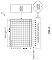
- FIG. 6 is a functional block diagram illustrating an embodiment of a SPAD imaging sensor, in accordance with an embodiment of the invention.
- Embodiments of a Stacked Chip SPAD Image Sensor are described herein.
- numerous specific details are set forth to provide a thorough understanding of the embodiments.
- One skilled in the relevant art will recognize, however, that the techniques described herein can be practiced without one or more of the specific details, or with other methods, components, materials, etc.
- well-known structures, materials, or operations are not shown or described in detail to avoid obscuring certain aspects.
- FIG. 1 is an exploded view of stacked device wafers 100 and 100 ′ that are to be bonded together to form an integrated circuit system 102 , in accordance with an embodiment of the invention.
- Device wafers 100 and 100 ′ may include silicon, gallium arsenide, or other semiconductor materials.
- device wafer 100 includes semiconductor dies 111 - 119 while device wafer 100 ′ includes corresponding semiconductor dies (view obscured in FIG. 1 ).
- each die 111 - 119 of device wafer 100 may include an array of Single-Photon Avalanche Diodes (SPADs), while each corresponding die of device wafer 100 ′ includes an array of digital counters and associated read-out electronics.
- SPADs Single-Photon Avalanche Diodes
- the placement of digital counters on the bottom device wafer 100 ′ allows for a very high fill factor in the SPAD array on the top device wafer 100 . Furthermore, since device wafer 100 is formed separately from device wafer 100 ′, custom fabrication processes may be utilized to optimize the formation of the SPAD array on device wafer 100 , while traditional CMOS processes may be retained when forming the CMOS circuitry on the device wafer 100 ′.
- FIG. 2A is a circuit diagram illustrating a stacked chip single-photon avalanche diode (SPAD) image sensor having a passive quench circuit in the top chip.
- the pixel circuitry illustrated in FIG. 2A e.g., PIXEL 1 , PIXEL 2 , etc.
- PIXEL 1 , PIXEL 2 , etc. is one possible pixel circuitry architecture for implementing each pixel with an imaging array, such as imaging array 605 , which will be discussed in more detail below.
- the pixels PIXEL 1 through PIXEL N are arranged in a single row. However, in other embodiments pixels of an imaging array may be arranged into a single column, or into a two-dimensional array of columns and rows.
- Each illustrated example of a pixel includes a single-photon avalanche diode (SPAD) and a passive quenching element (e.g., resistors R 1 -R N ) disposed on a top chip of a stacked chip system.
- SPAD single-photon avalanche diode
- R 1 -R N passive quenching element
- digital counters e.g., Digital Counters 1-N
- the digital counters are disposed on a bottom chip of the stacked chip system and are electrically coupled to receive output pulses 202 generated by a respective SPAD in response to a received photon.
- the digital counters may be enabled to count the number of output pulses 202 during a window of time and to output a digital signal 204 that is representative of the count.
- each digital counter includes an amplifier to amplify the received output pulse 202 .
- each digital counter is a 20-bit digital counter.
- the SPAD is reverse biased via a bias voltage VBIAS that is above the breakdown voltage of the SPAD.
- VBIAS bias voltage
- an avalanche multiplication process is triggered that causes an avalanche current at the output of the SPAD.
- This avalanche current self-quenches in response to a voltage drop that is developed across the quenching element (e.g., R 1 ), which causes the bias voltage across the SPAD to drop.
- the voltage across the SPAD recovers to above the bias voltage and then the SPAD is ready to be triggered again.
- the resulting output pulse 202 of the SPAD is received by a digital counter which increments its count in response thereto.
- FIG. 2B is a circuit diagram illustrating a stacked chip SPAD image sensor having a passive quench circuit in the bottom chip.
- the pixel circuitry illustrated in FIG. 2B e.g., PIXEL 1 , PIXEL 2 , etc.
- the pixel circuitry of FIG. 2B is similar in structure and operation to the pixel circuitry of FIG. 2A , described above, except the passive quenching elements (e.g., R 1 -R N ) are formed on the bottom chip.
- FIG. 2C is a circuit diagram illustrating a stacked chip SPAD image sensor having an active quench circuit in the bottom chip.
- the pixel circuitry illustrated in FIG. 2C e.g., PIXEL 1 , PIXEL 2 , etc.
- PIXEL 1 PIXEL 1
- PIXEL 2 PIXEL 2
- FIG. 2C each illustrated example of a pixel includes a single-photon avalanche diode (SPAD) and an active quenching element (e.g., AQ 1 -AQ N ).
- SPAD single-photon avalanche diode
- an active quenching element e.g., AQ 1 -AQ N
- the SPAD is reverse biased via a bias voltage VBIAS that is above the breakdown voltage of the SPAD.
- VBIAS bias voltage
- an avalanche multiplication process is triggered that causes an avalanche current at the output of the SPAD.
- the active quench circuit then senses this steep onset of avalanche current, generates a digital output pulse 206 , quickly reduces the bias voltage across the SPAD to below the breakdown voltage to quench the avalanche current, and then returns the bias voltage to above the breakdown voltage.
- the digital output pulse 206 is received by a digital counter which increments its count in response thereto.
- one advantage of implementing a stacked chip structure, as disclosed herein, is that an active quench circuit can be formed on a separate chip and thus not reduce the fill factor of the SPAD imaging array on the top chip.
- circuit diagrams of FIGS. 2A-2C are purely for illustrative purposes and that some circuit elements (e.g., passive components such as resistors and capacitors, and active components such as transistors) may have been omitted so as not to obscure the relevant teachings.
- the illustrated pixel circuitry of FIGS. 2A-2C may produce an output pulse that requires amplification prior to being sensed by the input of the digital counters.
- connection to the node between R1 and SPAD1 of FIGS. 2A and 2C would be at a high voltage that may require AC coupling.
- FIG. 3A is a cross-sectional view of an integrated circuit system 300 A having stacked device wafers 304 and 306 , in accordance with an embodiment of the invention.
- Integrated circuit system 300 A is one possible implementation of a portion of integrated circuit system 102 of FIG. 1 .
- the illustrated example of integrated circuit system 300 A includes a first device wafer 304 , a second device wafer 306 , and a bonding interface 308 .
- the first device wafer 304 includes a first semiconductor layer 310 and a first interconnect layer 312
- the second device wafer 306 is shown as including a second semiconductor layer 314 and a second interconnect layer 316 .
- Semiconductor layer 310 is shown as including semiconductor device 322 and interconnect layer 312 is shown as including metal layers 323 , oxide layer 324 , and vias 328 .
- Semiconductor layer 314 is shown as including semiconductor devices 318 and 320
- interconnect layer 316 is shown as including metal layers M 1 , M 2 , and M 3 , and dielectric layer 326 .
- semiconductor layer 310 and semiconductor layer 314 are layers of epitaxially grown silicon.
- semiconductor layer 314 includes semiconductor devices 318 and 320 formed in a front side of the semiconductor layer 314
- semiconductor layer 310 includes device 322 formed in a front side of semiconductor layer 310 .
- semiconductor device 322 includes a SPAD imaging array.
- the SPAD imaging array may include pixels arranged into several rows and several columns. Each pixel of the SPAD array may include a SPAD region formed in the front side and configured to receive photons from the backside of semiconductor layer 310 .
- Device 318 may include an array of digital counters.
- device 318 includes, at least, one digital counter for each SPAD region included in the SPAD imaging array.
- Device 320 may include associated peripheral circuitry, such as a readout circuit, a control circuit, or other function circuitry of an image sensor.
- device 318 further includes a storage device, such as random access memory, to act as a frame store to enable high-speed burst imaging capability.
- device wafers 304 and 306 may be bonded together to form an integrated circuit system, such as an imaging sensor system that includes devices on the first device wafer 304 as well as devices on the second device wafer 306 .
- devices 318 , 320 , and 322 may be formed in their respective semiconductor layer prior to bonding the device wafers 304 and 306 together.
- one or both of front side 307 and front side 309 are flattened by a chemical mechanical polish.
- dielectric layer 326 and interconnect layer 312 each include an oxide that are bonded together to form bonding interface 308 .
- FIG. 3B is a cross-sectional view of an integrated circuit system 300 B having stacked device wafers 304 , 306 , and 330 , in accordance with an embodiment of the invention.
- Integrated circuit system 300 B is one possible implementation of a portion of integrated circuit system 102 of FIG. 1 .
- the illustrated example of integrated circuit system 300 B includes first device wafer 304 , second device wafer 306 , third device wafer 330 and bonding interfaces 308 and 334 .
- First device wafer 304 and second device wafer 306 bond and operate as discussed above.
- integrated circuit system 300 B includes an additional third wafer 330 bonded to the second device wafer 306 .
- third wafer 330 includes a third semiconductor layer 332 and semiconductor device 336 formed in or on the third device wafer 330 .
- device 336 includes a storage device, such as random access memory (RAM), to act as a frame store to enable high-speed burst imaging capability.
- device 336 may be coupled to receive and store the outputs of the digital counters included in device 318 .
- RAM random access memory
- FIG. 4 is a cross-sectional view of an integrated circuit system 400 showing further detail of a SPAD imaging array with microlenses 404 , in accordance with an embodiment of the invention.
- system 400 includes SPAD regions 402 formed in semiconductor layer 310 .
- SPAD regions 402 may be one implementation of SPAD imaging array 322 of FIG. 3 .
- SPAD regions 402 may include any known SPAD design, including a guard-ring design.
- digital counters 406 formed in semiconductor layer 314 .
- Digital counters 406 are one possible implementation of the digital counters included in device 318 of FIG. 3 .
- FIG. 4 further illustrates that system 400 includes at least one digital counter 406 for each SPAD region 402 .
- having a separate digital counter 406 for each SPAD region allows for fast and simultaneous read-out of the SPAD regions 402 , allowing for a global shutter operation of the imaging sensor.
- formation of the digital counters 406 on a separate wafer allow for a substantial increase in the fill factor of the SPAD imaging array.
- Fill factor may refer to the ratio of the total area occupied by just the SPAD regions 402 to the total contiguous area occupied by the SPAD regions.
- the fill factor of the SPAD imaging array of FIG. 4 is very close to 100% in the 10 ⁇ m pixel pitch range.
- SPAD region 402 is coupled to digital counter 406 by way of metal traces 408 and 410 , and via 328 .
- vias 328 are micro-through silicon vias ( ⁇ TSVs).
- the ⁇ TSVs 328 may include a conductive material (e.g., copper, poly-silicon, etc.) deposited therein.
- ⁇ TSVs 328 may have an approximate diameter of less than about ten (10) micrometers, or in one embodiment, less than about five (5) micrometers.
- system 400 may include at least one via 328 for each SPAD region 402 to transfer output pulses generated by the SPAD region to the interconnect layer 316 of wafer 306 .
- Metal traces 408 and 410 may include a redistribution layer (RDL) comprising a thin-film (e.g., aluminum, copper, etc.) for rerouting and redistributing electrical connections between SPAD regions 402 and digital counters 406 .
- RDL redistribution layer
- the integrated circuit system 400 of FIG. 4 further includes several microlenses 404 .
- system 400 includes one microlens 404 for each SPAD region 402 .
- Microlens 404 is configured to direct (i.e., focus) incident photons onto SPAD region 402 .
- FIG. 5 is a cross-sectional view of an integrated circuit system 500 showing further detail of a SPAD imaging array with a color filter layer 502 and microlenses 402 , in accordance with an embodiment of the invention.
- color filter layer 502 is disposed on the backside of semiconductor layer 310 to filter light received by system 500 .
- color filter layer 502 includes at least one color filter (e.g., 504 A, 504 B, and 504 C) for each SPAD region 402 .
- a color filter may be configured to only allow light of a certain wavelength to pass through the color filter along to SPAD region 402 .
- color filter 504 A may be configured to allow blue light onto SPAD region 402 , while blocking red and green light.
- color filter 504 B may be configured to allow green light to pass through, while filtering out blue and red light.
- color filter 504 C may be configured to allow red light to pass, while filtering out blue and green light.
- system 500 includes microlenses 402 disposed on the color filter array 502 to direct incident photons through the color filter layer 502 to a respective SPAD region 402 .
- FIG. 6 is a functional block diagram illustrating an embodiment of a SPAD imaging sensor 600 , in accordance with an embodiment of the invention.
- SPAD imaging sensor 600 may be one implementation of at least one of the semiconductor devices mentioned previously, including devices 300 , 400 , and 500 , discussed above.
- the illustrated embodiment of image sensor 600 includes a SPAD imaging array 605 , high speed readout circuitry 610 , function logic 615 , and control circuitry 620 .
- Imaging array 605 is a two-dimensional (“2D”) array of backside illuminated imaging sensors or pixels (e.g., pixels P1, P2 . . . , Pn).
- each pixel includes a single-photon avalanche diode (SPAD).
- SPAD single-photon avalanche diode
- each pixel is arranged into a row (e.g., rows R1 to Ry) and a column (e.g., column C1 to Cx) to acquire image data of a person, place, or object, which can then be used to render a 2D image of the person, place, or object.
- Output pulses generated by the SPAD regions are read out by high speed readout circuitry 610 and transferred to function logic 615 .
- Readout circuitry 610 includes at least one digital counter for each of the SPAD regions and can also include amplification circuitry and/or quenching circuitry.
- Function logic 615 can simply store image data in memory or even manipulate the image data by applying post image effects (e.g., crop, rotate, remove red eye, adjust brightness, adjust contrast, or otherwise).
- Control circuitry 620 is coupled to imaging array 605 and/or to readout circuitry 610 to control operational characteristics of imaging array 605 .
- control circuitry 620 may simultaneously enable each of the digital counters included in high speed readout circuitry 610 for a window of time so as to implement a global shutter operation. Accordingly, embodiments of the SPAD stacked chip image sensor, discussed herein, provide for imaging that is both high speed and low light sensitive, which is typically not achieved with conventional sensor architectures.
Landscapes
- Engineering & Computer Science (AREA)
- Multimedia (AREA)
- Signal Processing (AREA)
- Solid State Image Pick-Up Elements (AREA)
Abstract
Description
Claims (20)
Priority Applications (4)
| Application Number | Priority Date | Filing Date | Title |
|---|---|---|---|
| US14/065,275 US9299732B2 (en) | 2013-10-28 | 2013-10-28 | Stacked chip SPAD image sensor |
| CN201410252328.2A CN104576667B (en) | 2013-10-28 | 2014-06-09 | Stacked chips SPAD imaging sensors |
| TW103124991A TWI543350B (en) | 2013-10-28 | 2014-07-21 | Stacked wafer single photon sag diode image sensor |
| HK15110230.2A HK1209897B (en) | 2013-10-28 | 2015-10-19 | Stacked chip spad image sensor |
Applications Claiming Priority (1)
| Application Number | Priority Date | Filing Date | Title |
|---|---|---|---|
| US14/065,275 US9299732B2 (en) | 2013-10-28 | 2013-10-28 | Stacked chip SPAD image sensor |
Publications (2)
| Publication Number | Publication Date |
|---|---|
| US20150115131A1 US20150115131A1 (en) | 2015-04-30 |
| US9299732B2 true US9299732B2 (en) | 2016-03-29 |
Family
ID=52994332
Family Applications (1)
| Application Number | Title | Priority Date | Filing Date |
|---|---|---|---|
| US14/065,275 Active 2034-02-08 US9299732B2 (en) | 2013-10-28 | 2013-10-28 | Stacked chip SPAD image sensor |
Country Status (3)
| Country | Link |
|---|---|
| US (1) | US9299732B2 (en) |
| CN (1) | CN104576667B (en) |
| TW (1) | TWI543350B (en) |
Cited By (37)
| Publication number | Priority date | Publication date | Assignee | Title |
|---|---|---|---|---|
| US10158038B1 (en) | 2018-05-17 | 2018-12-18 | Hi Llc | Fast-gated photodetector architectures comprising dual voltage sources with a switch configuration |
| US10177188B2 (en) | 2016-08-04 | 2019-01-08 | Samsung Electronics Co., Ltd. | Semiconductor package and method of fabricating the same |
| US10340408B1 (en) | 2018-05-17 | 2019-07-02 | Hi Llc | Non-invasive wearable brain interface systems including a headgear and a plurality of self-contained photodetector units configured to removably attach to the headgear |
| US20190378869A1 (en) * | 2018-05-17 | 2019-12-12 | Hi Llc | Wearable Systems with Stacked Photodetector Assemblies |
| US10868207B1 (en) | 2019-06-06 | 2020-12-15 | Hi Llc | Photodetector systems with low-power time-to-digital converter architectures to determine an arrival time of photon at a photodetector based on event detection time window |
| US10972692B2 (en) | 2019-02-12 | 2021-04-06 | Samsung Electronics Co., Ltd. | Image sensor including digital pixel |
| US11006876B2 (en) | 2018-12-21 | 2021-05-18 | Hi Llc | Biofeedback for awareness and modulation of mental state using a non-invasive brain interface system and method |
| US11081611B2 (en) | 2019-05-21 | 2021-08-03 | Hi Llc | Photodetector architectures for efficient fast-gating comprising a control system controlling a current drawn by an array of photodetectors with a single photon avalanche diode |
| US11096620B1 (en) | 2020-02-21 | 2021-08-24 | Hi Llc | Wearable module assemblies for an optical measurement system |
| US11187575B2 (en) | 2020-03-20 | 2021-11-30 | Hi Llc | High density optical measurement systems with minimal number of light sources |
| US11213245B2 (en) | 2018-06-20 | 2022-01-04 | Hi Llc | Spatial and temporal-based diffusive correlation spectroscopy systems and methods |
| US11213206B2 (en) | 2018-07-17 | 2022-01-04 | Hi Llc | Non-invasive measurement systems with single-photon counting camera |
| US11221400B2 (en) | 2018-03-27 | 2022-01-11 | Omnivision Technologies, Inc. | Dual mode stacked photomultipliers suitable for use in long range time of flight applications |
| US11245404B2 (en) | 2020-03-20 | 2022-02-08 | Hi Llc | Phase lock loop circuit based signal generation in an optical measurement system |
| US11380722B2 (en) | 2019-02-08 | 2022-07-05 | Samsung Electronics Co., Ltd. | Image sensor device |
| US11515014B2 (en) | 2020-02-21 | 2022-11-29 | Hi Llc | Methods and systems for initiating and conducting a customized computer-enabled brain research study |
| US11607132B2 (en) | 2020-03-20 | 2023-03-21 | Hi Llc | Temporal resolution control for temporal point spread function generation in an optical measurement system |
| US11630310B2 (en) | 2020-02-21 | 2023-04-18 | Hi Llc | Wearable devices and wearable assemblies with adjustable positioning for use in an optical measurement system |
| US11645483B2 (en) | 2020-03-20 | 2023-05-09 | Hi Llc | Phase lock loop circuit based adjustment of a measurement time window in an optical measurement system |
| US11771362B2 (en) | 2020-02-21 | 2023-10-03 | Hi Llc | Integrated detector assemblies for a wearable module of an optical measurement system |
| US11813041B2 (en) | 2019-05-06 | 2023-11-14 | Hi Llc | Photodetector architectures for time-correlated single photon counting |
| US11819311B2 (en) | 2020-03-20 | 2023-11-21 | Hi Llc | Maintaining consistent photodetector sensitivity in an optical measurement system |
| US11857348B2 (en) | 2020-03-20 | 2024-01-02 | Hi Llc | Techniques for determining a timing uncertainty of a component of an optical measurement system |
| US11864867B2 (en) | 2020-03-20 | 2024-01-09 | Hi Llc | Control circuit for a light source in an optical measurement system by applying voltage with a first polarity to start an emission of a light pulse and applying voltage with a second polarity to stop the emission of the light pulse |
| US11877825B2 (en) | 2020-03-20 | 2024-01-23 | Hi Llc | Device enumeration in an optical measurement system |
| US11883181B2 (en) | 2020-02-21 | 2024-01-30 | Hi Llc | Multimodal wearable measurement systems and methods |
| US11903676B2 (en) | 2020-03-20 | 2024-02-20 | Hi Llc | Photodetector calibration of an optical measurement system |
| US11950879B2 (en) | 2020-02-21 | 2024-04-09 | Hi Llc | Estimation of source-detector separation in an optical measurement system |
| US11969259B2 (en) | 2020-02-21 | 2024-04-30 | Hi Llc | Detector assemblies for a wearable module of an optical measurement system and including spring-loaded light-receiving members |
| US12029558B2 (en) | 2020-02-21 | 2024-07-09 | Hi Llc | Time domain-based optical measurement systems and methods configured to measure absolute properties of tissue |
| US12059262B2 (en) | 2020-03-20 | 2024-08-13 | Hi Llc | Maintaining consistent photodetector sensitivity in an optical measurement system |
| US12059270B2 (en) | 2020-04-24 | 2024-08-13 | Hi Llc | Systems and methods for noise removal in an optical measurement system |
| US12085789B2 (en) | 2020-03-20 | 2024-09-10 | Hi Llc | Bias voltage generation in an optical measurement system |
| US12138068B2 (en) | 2020-03-20 | 2024-11-12 | Hi Llc | Techniques for characterizing a nonlinearity of a time-to-digital converter in an optical measurement system |
| US12144653B2 (en) | 2020-02-21 | 2024-11-19 | Hi Llc | Systems, circuits, and methods for reducing common-mode noise in biopotential recordings |
| US12283639B2 (en) | 2021-12-31 | 2025-04-22 | Trupixel Inc. | Single-photon detection pixel and single-photon detection pixel array including the same |
| US12402426B2 (en) | 2021-08-31 | 2025-08-26 | Trupixel Inc. | Single-photon detection device, single-photon detector, and single-photon detector array |
Families Citing this family (50)
| Publication number | Priority date | Publication date | Assignee | Title |
|---|---|---|---|---|
| US9628735B2 (en) * | 2015-06-22 | 2017-04-18 | Omnivision Technologies, Inc. | Imaging systems with single-photon-avalanche-diodes and sensor translation, and associated methods |
| US9704827B2 (en) | 2015-06-25 | 2017-07-11 | Taiwan Semiconductor Manufacturing Co., Ltd. | Hybrid bond pad structure |
| US10007007B2 (en) * | 2015-09-08 | 2018-06-26 | Shenzhen Xpectvision Technology Co., Ltd. | Methods for making an X-ray detector |
| US9992477B2 (en) | 2015-09-24 | 2018-06-05 | Ouster, Inc. | Optical system for collecting distance information within a field |
| KR101785793B1 (en) * | 2015-10-27 | 2017-11-15 | 연세대학교 산학협력단 | Internal device and diagnosis apparatus employing the same |
| US10014340B2 (en) * | 2015-12-28 | 2018-07-03 | Taiwan Semiconductor Manufacturing Co., Ltd. | Stacked SPAD image sensor |
| ES2843101T3 (en) | 2016-03-15 | 2021-07-15 | Dartmouth College | Quanta backlit stacked image sensor with parallel cluster reading |
| WO2017183477A1 (en) * | 2016-04-22 | 2017-10-26 | ソニー株式会社 | Solid-state imaging element, driving method, and electronic device |
| US10269854B2 (en) * | 2016-04-26 | 2019-04-23 | Taiwan Semiconductor Manufacturing Co., Ltd. | Rerouting method and a structure for stacked image sensors |
| GB2551483B (en) * | 2016-06-13 | 2020-05-27 | Toshiba Res Europe Limited | A photon detection device and a method of manufacturing a photon detection device |
| EP3472866A4 (en) * | 2016-06-21 | 2020-02-12 | Shenzhen Genorivision Technology Co., Ltd. | IMAGE SENSOR WITH LARGE DYNAMIC RANGE |
| US10545193B2 (en) | 2016-07-13 | 2020-01-28 | Stmicroelectronics (Research & Development) Limited | Charge pump overload detection |
| KR102460077B1 (en) | 2016-08-05 | 2022-10-28 | 삼성전자주식회사 | Stacked Image Sensor Package And Stacked Image Sensor Module |
| EP3387676B1 (en) * | 2016-10-18 | 2024-12-04 | Sony Semiconductor Solutions Corporation | Photodetector |
| GB201704203D0 (en) | 2017-03-16 | 2017-05-03 | Pixquanta Ltd | An electromagnetic radiation detection device |
| JP6929671B2 (en) | 2017-03-17 | 2021-09-01 | キヤノン株式会社 | Imaging device and imaging system |
| US10312275B2 (en) | 2017-04-25 | 2019-06-04 | Semiconductor Components Industries, Llc | Single-photon avalanche diode image sensor with photon counting and time-of-flight detection capabilities |
| KR102395588B1 (en) * | 2017-09-18 | 2022-05-09 | 에이에스엠엘 네델란즈 비.브이. | Field programmable detector array |
| US10636930B2 (en) * | 2017-09-29 | 2020-04-28 | Taiwan Semiconductor Manufacturing Company Ltd. | SPAD image sensor and associated fabricating method |
| US10204950B1 (en) * | 2017-09-29 | 2019-02-12 | Taiwan Semiconductor Manufacturing Company Ltd. | SPAD image sensor and associated fabricating method |
| WO2019146725A1 (en) * | 2018-01-26 | 2019-08-01 | 浜松ホトニクス株式会社 | Photodetector device |
| KR102799594B1 (en) * | 2018-01-26 | 2025-04-23 | 하마마츠 포토닉스 가부시키가이샤 | Light detection device |
| JP7114264B2 (en) | 2018-02-09 | 2022-08-08 | キヤノン株式会社 | Photoelectric conversion device and imaging system |
| JP7039310B2 (en) | 2018-02-09 | 2022-03-22 | キヤノン株式会社 | Photoelectric conversion device and imaging system |
| US11089251B2 (en) * | 2018-07-12 | 2021-08-10 | Canon Kabushiki Kaisha | Image sensor and image capturing apparatus |
| JP7261005B2 (en) * | 2018-12-26 | 2023-04-19 | キヤノン株式会社 | IMAGE PROCESSING DEVICE AND METHOD, IMAGING DEVICE, AND IMAGE SENSOR CONTROL METHOD |
| WO2020144211A1 (en) * | 2019-01-11 | 2020-07-16 | PixQuanta Limited | An electromagnetic radiation detection device |
| JP7321713B2 (en) * | 2019-01-30 | 2023-08-07 | キヤノン株式会社 | Photoelectric conversion device, imaging system, moving body |
| JP7327949B2 (en) | 2019-02-27 | 2023-08-16 | キヤノン株式会社 | Photoelectric conversion device, photoelectric conversion system, and moving body |
| US10784302B1 (en) | 2019-03-07 | 2020-09-22 | Semiconductor Components Industries, Llc | Semiconductor device with single-photon avalanche diode pixels and a light attenuating layer |
| JP7292135B2 (en) * | 2019-07-09 | 2023-06-16 | キヤノン株式会社 | Imaging element and imaging device |
| JP7679169B2 (en) | 2019-08-08 | 2025-05-19 | キヤノン株式会社 | Photoelectric conversion device, photoelectric conversion system |
| US11398516B2 (en) | 2019-08-29 | 2022-07-26 | Taiwan Semiconductor Manufacturing Company, Ltd. | Conductive contact for ion through-substrate via |
| DE102020101246B4 (en) | 2019-08-29 | 2025-03-27 | Taiwan Semiconductor Manufacturing Co. Ltd. | Substrate via with doped channel region and corresponding manufacturing process |
| JP7535704B2 (en) * | 2019-09-06 | 2024-08-19 | パナソニックIpマネジメント株式会社 | Imaging device |
| JP7478526B2 (en) | 2019-09-27 | 2024-05-07 | ソニーセミコンダクタソリューションズ株式会社 | Solid-state imaging device and ranging system |
| JP7757026B2 (en) | 2019-11-20 | 2025-10-21 | キヤノン株式会社 | Imaging device, imaging system, and mobile object |
| WO2021148603A1 (en) * | 2020-01-22 | 2021-07-29 | MAX-PLANCK-Gesellschaft zur Förderung der Wissenschaften e.V. | A semiconductor photomultiplier module comprising a stacked configuration of a sensor chip and electronic readout chips |
| JP7492338B2 (en) | 2020-01-30 | 2024-05-29 | キヤノン株式会社 | Photoelectric conversion device, photoelectric conversion system and mobile body |
| US11646335B2 (en) * | 2020-01-30 | 2023-05-09 | Semiconductor Components Industries, Llc | Semiconductor devices with single-photon avalanche diodes and rectangular microlenses |
| US11554589B2 (en) | 2020-02-19 | 2023-01-17 | Canon Kabushiki Kaisha | Liquid container and method of manufacturing the same |
| JP7527853B2 (en) | 2020-06-11 | 2024-08-05 | キヤノン株式会社 | Photoelectric conversion device |
| FR3115158B1 (en) * | 2020-10-12 | 2022-10-14 | St Microelectronics Res & Dev Ltd | Pixel to SPAD |
| CN112397542B (en) * | 2020-11-16 | 2023-04-07 | Oppo(重庆)智能科技有限公司 | Image sensing module, time flight device and electronic equipment |
| JP7604204B2 (en) | 2020-12-10 | 2024-12-23 | キヤノン株式会社 | Photoelectric conversion device, imaging system, and mobile object |
| US11855106B2 (en) * | 2021-01-22 | 2023-12-26 | Canon Kabushiki Kaisha | Signal processing device having counter counting pulses from avalanche photodiode |
| CN113782510B (en) * | 2021-11-12 | 2022-04-01 | 深圳市灵明光子科技有限公司 | 3d stacks bonding key of chip and lays structure |
| CN114284306A (en) * | 2021-12-15 | 2022-04-05 | 武汉新芯集成电路制造有限公司 | Depth and image sensor device, manufacturing method thereof and depth and image sensor chip |
| JP7830519B2 (en) | 2022-01-05 | 2026-03-16 | キヤノン株式会社 | Photoelectric converter, photoelectric converter system, and mobile body |
| JP2023183169A (en) * | 2022-06-15 | 2023-12-27 | ソニーセミコンダクタソリューションズ株式会社 | light detection element |
Citations (9)
| Publication number | Priority date | Publication date | Assignee | Title |
|---|---|---|---|---|
| US20080083959A1 (en) * | 2006-10-06 | 2008-04-10 | Taiwan Semiconductor Manufacturing Co., Ltd. | Stacked structures and methods of forming stacked structures |
| US20110050969A1 (en) * | 2009-08-28 | 2011-03-03 | Sony Corporation | Imaging device and camera system |
| US20110101481A1 (en) * | 2009-11-04 | 2011-05-05 | Hidetoshi Nozaki | Photodetector Array Having Array of Discrete Electron Repulsive Elements |
| US20110248396A1 (en) * | 2010-04-09 | 2011-10-13 | International Business Machines Corporation | Bow-balanced 3d chip stacking |
| US20120326009A1 (en) * | 2011-02-04 | 2012-12-27 | Kenneth Edward Salsman | Plasmonic light sensors |
| US20130032713A1 (en) * | 2011-08-05 | 2013-02-07 | Barbi Nicholas C | Electron detector including one or more intimately-coupled scintillator-photomultiplier combinations, and electron microscope employing same |
| US20130056866A1 (en) * | 2011-09-02 | 2013-03-07 | Maxim Integrated Products, Inc. | Stacked wafer-level package device |
| WO2013058001A1 (en) * | 2011-10-21 | 2013-04-25 | 浜松ホトニクス株式会社 | Light detection device |
| US8860850B1 (en) * | 2007-05-22 | 2014-10-14 | Rockwell Collins, Inc. | Photon-starved imaging system |
Family Cites Families (1)
| Publication number | Priority date | Publication date | Assignee | Title |
|---|---|---|---|---|
| US8446503B1 (en) * | 2007-05-22 | 2013-05-21 | Rockwell Collins, Inc. | Imaging system |
-
2013
- 2013-10-28 US US14/065,275 patent/US9299732B2/en active Active
-
2014
- 2014-06-09 CN CN201410252328.2A patent/CN104576667B/en active Active
- 2014-07-21 TW TW103124991A patent/TWI543350B/en active
Patent Citations (10)
| Publication number | Priority date | Publication date | Assignee | Title |
|---|---|---|---|---|
| US20080083959A1 (en) * | 2006-10-06 | 2008-04-10 | Taiwan Semiconductor Manufacturing Co., Ltd. | Stacked structures and methods of forming stacked structures |
| US8860850B1 (en) * | 2007-05-22 | 2014-10-14 | Rockwell Collins, Inc. | Photon-starved imaging system |
| US20110050969A1 (en) * | 2009-08-28 | 2011-03-03 | Sony Corporation | Imaging device and camera system |
| US20110101481A1 (en) * | 2009-11-04 | 2011-05-05 | Hidetoshi Nozaki | Photodetector Array Having Array of Discrete Electron Repulsive Elements |
| US20110248396A1 (en) * | 2010-04-09 | 2011-10-13 | International Business Machines Corporation | Bow-balanced 3d chip stacking |
| US20120326009A1 (en) * | 2011-02-04 | 2012-12-27 | Kenneth Edward Salsman | Plasmonic light sensors |
| US20130032713A1 (en) * | 2011-08-05 | 2013-02-07 | Barbi Nicholas C | Electron detector including one or more intimately-coupled scintillator-photomultiplier combinations, and electron microscope employing same |
| US20130056866A1 (en) * | 2011-09-02 | 2013-03-07 | Maxim Integrated Products, Inc. | Stacked wafer-level package device |
| WO2013058001A1 (en) * | 2011-10-21 | 2013-04-25 | 浜松ホトニクス株式会社 | Light detection device |
| US20140291486A1 (en) * | 2011-10-21 | 2014-10-02 | Hamamatsu Photonics K.K. | Light detection device |
Cited By (49)
| Publication number | Priority date | Publication date | Assignee | Title |
|---|---|---|---|---|
| US10868073B2 (en) | 2016-08-04 | 2020-12-15 | Samsung Electronics Co., Ltd. | Method of fabricating semiconductor package |
| US10177188B2 (en) | 2016-08-04 | 2019-01-08 | Samsung Electronics Co., Ltd. | Semiconductor package and method of fabricating the same |
| US11482554B2 (en) | 2016-08-04 | 2022-10-25 | Samsung Electronics Co., Ltd. | Semiconductor package and method of fabricating the same |
| US11221400B2 (en) | 2018-03-27 | 2022-01-11 | Omnivision Technologies, Inc. | Dual mode stacked photomultipliers suitable for use in long range time of flight applications |
| US11004998B2 (en) | 2018-05-17 | 2021-05-11 | Hi Llc | Wearable brain interface systems including a headgear and a plurality of photodetector units |
| US11437538B2 (en) | 2018-05-17 | 2022-09-06 | Hi Llc | Wearable brain interface systems including a headgear and a plurality of photodetector units each housing a photodetector configured to be controlled by a master control unit |
| US10672936B2 (en) | 2018-05-17 | 2020-06-02 | Hi Llc | Wearable systems with fast-gated photodetector architectures having a single photon avalanche diode and capacitor |
| US10672935B2 (en) | 2018-05-17 | 2020-06-02 | Hi Llc | Non-invasive wearable brain interface systems including a headgear and a plurality of self-contained photodetector units |
| US10847563B2 (en) * | 2018-05-17 | 2020-11-24 | Hi Llc | Wearable systems with stacked photodetector assemblies |
| US20190378869A1 (en) * | 2018-05-17 | 2019-12-12 | Hi Llc | Wearable Systems with Stacked Photodetector Assemblies |
| US10340408B1 (en) | 2018-05-17 | 2019-07-02 | Hi Llc | Non-invasive wearable brain interface systems including a headgear and a plurality of self-contained photodetector units configured to removably attach to the headgear |
| US10515993B2 (en) * | 2018-05-17 | 2019-12-24 | Hi Llc | Stacked photodetector assemblies |
| US10158038B1 (en) | 2018-05-17 | 2018-12-18 | Hi Llc | Fast-gated photodetector architectures comprising dual voltage sources with a switch configuration |
| US10424683B1 (en) | 2018-05-17 | 2019-09-24 | Hi Llc | Photodetector comprising a single photon avalanche diode and a capacitor |
| US11213245B2 (en) | 2018-06-20 | 2022-01-04 | Hi Llc | Spatial and temporal-based diffusive correlation spectroscopy systems and methods |
| US11213206B2 (en) | 2018-07-17 | 2022-01-04 | Hi Llc | Non-invasive measurement systems with single-photon counting camera |
| US11006876B2 (en) | 2018-12-21 | 2021-05-18 | Hi Llc | Biofeedback for awareness and modulation of mental state using a non-invasive brain interface system and method |
| US11903713B2 (en) | 2018-12-21 | 2024-02-20 | Hi Llc | Biofeedback for awareness and modulation of mental state using a non-invasive brain interface system and method |
| US12176362B2 (en) | 2019-02-08 | 2024-12-24 | Samsung Electronics Co., Ltd. | Image sensor device |
| US11380722B2 (en) | 2019-02-08 | 2022-07-05 | Samsung Electronics Co., Ltd. | Image sensor device |
| US10972692B2 (en) | 2019-02-12 | 2021-04-06 | Samsung Electronics Co., Ltd. | Image sensor including digital pixel |
| US11813041B2 (en) | 2019-05-06 | 2023-11-14 | Hi Llc | Photodetector architectures for time-correlated single photon counting |
| US11081611B2 (en) | 2019-05-21 | 2021-08-03 | Hi Llc | Photodetector architectures for efficient fast-gating comprising a control system controlling a current drawn by an array of photodetectors with a single photon avalanche diode |
| US11398578B2 (en) | 2019-06-06 | 2022-07-26 | Hi Llc | Photodetector systems with low-power time-to-digital converter architectures to determine an arrival time of photon at a photodetector based on event detection time window |
| US10868207B1 (en) | 2019-06-06 | 2020-12-15 | Hi Llc | Photodetector systems with low-power time-to-digital converter architectures to determine an arrival time of photon at a photodetector based on event detection time window |
| US11950879B2 (en) | 2020-02-21 | 2024-04-09 | Hi Llc | Estimation of source-detector separation in an optical measurement system |
| US11883181B2 (en) | 2020-02-21 | 2024-01-30 | Hi Llc | Multimodal wearable measurement systems and methods |
| US11096620B1 (en) | 2020-02-21 | 2021-08-24 | Hi Llc | Wearable module assemblies for an optical measurement system |
| US11630310B2 (en) | 2020-02-21 | 2023-04-18 | Hi Llc | Wearable devices and wearable assemblies with adjustable positioning for use in an optical measurement system |
| US11771362B2 (en) | 2020-02-21 | 2023-10-03 | Hi Llc | Integrated detector assemblies for a wearable module of an optical measurement system |
| US12144653B2 (en) | 2020-02-21 | 2024-11-19 | Hi Llc | Systems, circuits, and methods for reducing common-mode noise in biopotential recordings |
| US12029558B2 (en) | 2020-02-21 | 2024-07-09 | Hi Llc | Time domain-based optical measurement systems and methods configured to measure absolute properties of tissue |
| US11969259B2 (en) | 2020-02-21 | 2024-04-30 | Hi Llc | Detector assemblies for a wearable module of an optical measurement system and including spring-loaded light-receiving members |
| US11515014B2 (en) | 2020-02-21 | 2022-11-29 | Hi Llc | Methods and systems for initiating and conducting a customized computer-enabled brain research study |
| US11903676B2 (en) | 2020-03-20 | 2024-02-20 | Hi Llc | Photodetector calibration of an optical measurement system |
| US12059262B2 (en) | 2020-03-20 | 2024-08-13 | Hi Llc | Maintaining consistent photodetector sensitivity in an optical measurement system |
| US11864867B2 (en) | 2020-03-20 | 2024-01-09 | Hi Llc | Control circuit for a light source in an optical measurement system by applying voltage with a first polarity to start an emission of a light pulse and applying voltage with a second polarity to stop the emission of the light pulse |
| US11187575B2 (en) | 2020-03-20 | 2021-11-30 | Hi Llc | High density optical measurement systems with minimal number of light sources |
| US11607132B2 (en) | 2020-03-20 | 2023-03-21 | Hi Llc | Temporal resolution control for temporal point spread function generation in an optical measurement system |
| US11857348B2 (en) | 2020-03-20 | 2024-01-02 | Hi Llc | Techniques for determining a timing uncertainty of a component of an optical measurement system |
| US11819311B2 (en) | 2020-03-20 | 2023-11-21 | Hi Llc | Maintaining consistent photodetector sensitivity in an optical measurement system |
| US11877825B2 (en) | 2020-03-20 | 2024-01-23 | Hi Llc | Device enumeration in an optical measurement system |
| US11245404B2 (en) | 2020-03-20 | 2022-02-08 | Hi Llc | Phase lock loop circuit based signal generation in an optical measurement system |
| US12085789B2 (en) | 2020-03-20 | 2024-09-10 | Hi Llc | Bias voltage generation in an optical measurement system |
| US12138068B2 (en) | 2020-03-20 | 2024-11-12 | Hi Llc | Techniques for characterizing a nonlinearity of a time-to-digital converter in an optical measurement system |
| US11645483B2 (en) | 2020-03-20 | 2023-05-09 | Hi Llc | Phase lock loop circuit based adjustment of a measurement time window in an optical measurement system |
| US12059270B2 (en) | 2020-04-24 | 2024-08-13 | Hi Llc | Systems and methods for noise removal in an optical measurement system |
| US12402426B2 (en) | 2021-08-31 | 2025-08-26 | Trupixel Inc. | Single-photon detection device, single-photon detector, and single-photon detector array |
| US12283639B2 (en) | 2021-12-31 | 2025-04-22 | Trupixel Inc. | Single-photon detection pixel and single-photon detection pixel array including the same |
Also Published As
| Publication number | Publication date |
|---|---|
| US20150115131A1 (en) | 2015-04-30 |
| HK1209897A1 (en) | 2016-04-08 |
| TW201523847A (en) | 2015-06-16 |
| TWI543350B (en) | 2016-07-21 |
| CN104576667B (en) | 2017-08-11 |
| CN104576667A (en) | 2015-04-29 |
Similar Documents
| Publication | Publication Date | Title |
|---|---|---|
| US9299732B2 (en) | Stacked chip SPAD image sensor | |
| US9312401B2 (en) | Single photon avalanche diode imaging sensor for complementary metal oxide semiconductor stacked chip applications | |
| US9331116B2 (en) | Back side illuminated single photon avalanche diode imaging sensor with high short wavelength detection efficiency | |
| US10050168B2 (en) | Back side illuminated image sensor with guard ring region reflecting structure | |
| US11764314B2 (en) | Scattering structures for single-photon avalanche diodes | |
| US9608027B2 (en) | Stacked embedded SPAD image sensor for attached 3D information | |
| US20180026147A1 (en) | Vertical gate guard ring for single photon avalanche diode pitch minimization | |
| US12027633B2 (en) | Scattering structures for single-photon avalanche diodes | |
| US12113138B2 (en) | Semiconductor devices with single-photon avalanche diodes and light scattering structures | |
| US11646335B2 (en) | Semiconductor devices with single-photon avalanche diodes and rectangular microlenses | |
| HK1209897B (en) | Stacked chip spad image sensor | |
| US20260123075A1 (en) | Semiconductor device with optical structure for enhancing blue light detection | |
| TWI813103B (en) | Semiconductor device and semiconductor die | |
| HK1208286B (en) | Single photon avalanche diode imaging sensor for complementary metal oxide semiconductor stacked chip applications | |
| HK1208285B (en) | Back side illuminated single photon avalanche diode and imaging sensor system comprising the same | |
| CN121985611A (en) | Semiconductor device having optical structure for enhanced blue light detection | |
| HK1218347B (en) | Back side illuminated image sensor with guard ring region reflecting structure | |
| HK1222485A1 (en) | Blue enhanced image sensor |
Legal Events
| Date | Code | Title | Description |
|---|---|---|---|
| AS | Assignment |
Owner name: OMNIVISION TECHNOLOGIES, INC., CALIFORNIA Free format text: ASSIGNMENT OF ASSIGNORS INTEREST;ASSIGNORS:WEBSTER, ERIC A.G.;DAI, TIEJUN;REEL/FRAME:031498/0971 Effective date: 20131028 |
|
| STCF | Information on status: patent grant |
Free format text: PATENTED CASE |
|
| MAFP | Maintenance fee payment |
Free format text: PAYMENT OF MAINTENANCE FEE, 4TH YEAR, LARGE ENTITY (ORIGINAL EVENT CODE: M1551); ENTITY STATUS OF PATENT OWNER: LARGE ENTITY Year of fee payment: 4 |
|
| MAFP | Maintenance fee payment |
Free format text: PAYMENT OF MAINTENANCE FEE, 8TH YEAR, LARGE ENTITY (ORIGINAL EVENT CODE: M1552); ENTITY STATUS OF PATENT OWNER: LARGE ENTITY Year of fee payment: 8 |