US9274448B2 - Image forming apparatus, positional deviation detection apparatus, and positional deviation detection method - Google Patents
Image forming apparatus, positional deviation detection apparatus, and positional deviation detection method Download PDFInfo
- Publication number
- US9274448B2 US9274448B2 US14/480,428 US201414480428A US9274448B2 US 9274448 B2 US9274448 B2 US 9274448B2 US 201414480428 A US201414480428 A US 201414480428A US 9274448 B2 US9274448 B2 US 9274448B2
- Authority
- US
- United States
- Prior art keywords
- positional deviation
- deviation correction
- correction pattern
- detection unit
- patch
- Prior art date
- Legal status (The legal status is an assumption and is not a legal conclusion. Google has not performed a legal analysis and makes no representation as to the accuracy of the status listed.)
- Active
Links
- 238000001514 detection method Methods 0.000 title claims abstract description 142
- 238000012937 correction Methods 0.000 claims abstract description 102
- 238000000034 method Methods 0.000 claims description 73
- 238000011161 development Methods 0.000 claims description 18
- 230000001788 irregular Effects 0.000 claims description 3
- 238000012546 transfer Methods 0.000 description 116
- 230000008859 change Effects 0.000 description 32
- 239000000126 substance Substances 0.000 description 14
- 239000003086 colorant Substances 0.000 description 13
- 230000006866 deterioration Effects 0.000 description 12
- 230000015572 biosynthetic process Effects 0.000 description 10
- 239000000463 material Substances 0.000 description 10
- 230000003287 optical effect Effects 0.000 description 8
- 230000000630 rising effect Effects 0.000 description 8
- 230000009467 reduction Effects 0.000 description 7
- 230000035945 sensitivity Effects 0.000 description 4
- 239000000758 substrate Substances 0.000 description 4
- 230000007423 decrease Effects 0.000 description 3
- 238000010586 diagram Methods 0.000 description 3
- 238000011895 specific detection Methods 0.000 description 3
- 230000002123 temporal effect Effects 0.000 description 3
- 238000012935 Averaging Methods 0.000 description 2
- 238000004140 cleaning Methods 0.000 description 2
- 230000002542 deteriorative effect Effects 0.000 description 2
- 238000005259 measurement Methods 0.000 description 2
- 238000012545 processing Methods 0.000 description 2
- 230000002441 reversible effect Effects 0.000 description 2
- 239000007787 solid Substances 0.000 description 2
- 238000011144 upstream manufacturing Methods 0.000 description 2
- 230000008901 benefit Effects 0.000 description 1
- 230000003111 delayed effect Effects 0.000 description 1
- 238000003708 edge detection Methods 0.000 description 1
- 230000006870 function Effects 0.000 description 1
- 230000006872 improvement Effects 0.000 description 1
- 230000007246 mechanism Effects 0.000 description 1
- 238000012986 modification Methods 0.000 description 1
- 230000004048 modification Effects 0.000 description 1
- 230000008569 process Effects 0.000 description 1
- 239000011347 resin Substances 0.000 description 1
- 229920005989 resin Polymers 0.000 description 1
- 238000005549 size reduction Methods 0.000 description 1
Images


Classifications
-
- G—PHYSICS
- G03—PHOTOGRAPHY; CINEMATOGRAPHY; ANALOGOUS TECHNIQUES USING WAVES OTHER THAN OPTICAL WAVES; ELECTROGRAPHY; HOLOGRAPHY
- G03G—ELECTROGRAPHY; ELECTROPHOTOGRAPHY; MAGNETOGRAPHY
- G03G15/00—Apparatus for electrographic processes using a charge pattern
- G03G15/50—Machine control of apparatus for electrographic processes using a charge pattern, e.g. regulating differents parts of the machine, multimode copiers, microprocessor control
- G03G15/5054—Machine control of apparatus for electrographic processes using a charge pattern, e.g. regulating differents parts of the machine, multimode copiers, microprocessor control by measuring the characteristics of an intermediate image carrying member or the characteristics of an image on an intermediate image carrying member, e.g. intermediate transfer belt or drum, conveyor belt
- G03G15/5058—Machine control of apparatus for electrographic processes using a charge pattern, e.g. regulating differents parts of the machine, multimode copiers, microprocessor control by measuring the characteristics of an intermediate image carrying member or the characteristics of an image on an intermediate image carrying member, e.g. intermediate transfer belt or drum, conveyor belt using a test patch
-
- G—PHYSICS
- G03—PHOTOGRAPHY; CINEMATOGRAPHY; ANALOGOUS TECHNIQUES USING WAVES OTHER THAN OPTICAL WAVES; ELECTROGRAPHY; HOLOGRAPHY
- G03G—ELECTROGRAPHY; ELECTROPHOTOGRAPHY; MAGNETOGRAPHY
- G03G15/00—Apparatus for electrographic processes using a charge pattern
- G03G15/01—Apparatus for electrographic processes using a charge pattern for producing multicoloured copies
- G03G15/0105—Details of unit
- G03G15/0121—Details of unit for developing
-
- G—PHYSICS
- G03—PHOTOGRAPHY; CINEMATOGRAPHY; ANALOGOUS TECHNIQUES USING WAVES OTHER THAN OPTICAL WAVES; ELECTROGRAPHY; HOLOGRAPHY
- G03G—ELECTROGRAPHY; ELECTROPHOTOGRAPHY; MAGNETOGRAPHY
- G03G15/00—Apparatus for electrographic processes using a charge pattern
- G03G15/01—Apparatus for electrographic processes using a charge pattern for producing multicoloured copies
- G03G15/0105—Details of unit
- G03G15/0126—Details of unit using a solid developer
-
- G—PHYSICS
- G03—PHOTOGRAPHY; CINEMATOGRAPHY; ANALOGOUS TECHNIQUES USING WAVES OTHER THAN OPTICAL WAVES; ELECTROGRAPHY; HOLOGRAPHY
- G03G—ELECTROGRAPHY; ELECTROPHOTOGRAPHY; MAGNETOGRAPHY
- G03G2215/00—Apparatus for electrophotographic processes
- G03G2215/01—Apparatus for electrophotographic processes for producing multicoloured copies
- G03G2215/0167—Apparatus for electrophotographic processes for producing multicoloured copies single electrographic recording member
- G03G2215/0187—Multicoloured toner image formed on the recording member
-
- G—PHYSICS
- G03—PHOTOGRAPHY; CINEMATOGRAPHY; ANALOGOUS TECHNIQUES USING WAVES OTHER THAN OPTICAL WAVES; ELECTROGRAPHY; HOLOGRAPHY
- G03G—ELECTROGRAPHY; ELECTROPHOTOGRAPHY; MAGNETOGRAPHY
- G03G2215/00—Apparatus for electrophotographic processes
- G03G2215/06—Developing structures, details
- G03G2215/0634—Developing device
- G03G2215/0636—Specific type of dry developer device
- G03G2215/0648—Two or more donor members
Definitions
- the present invention relates to an image forming apparatus such as, mainly, an electrophotographic or electrostatic copying machine and printer, that can correct a positional deviation in an image. Further, the present invention relates to a positional deviation detection apparatus and a positional deviation detection method for detecting a positional deviation in an image.
- the color image is made of, for example, a yellow (Y) toner, a magenta (M) toner, a cyan (C) toner, and a black (Bk) toner.
- Y yellow
- M magenta
- C cyan
- Bk black
- An arbitrary color image can be formed by superimposing toner images formed from the toners of the respective colors on one another.
- electrophotographic color image forming apparatuses may form the toner images of the respective colors with a deviation generated among relative positions thereof due to tolerances of rotational speeds of image bearing members that bear the toners of the plurality of colors, a temperature change in the apparatus, an error in relative positions of a driving member and an image forming member, a change over time, and the like.
- This is a state with a so-called color deviation generated in a color image.
- the deviation among the relative positions of the toner images of the respective colors also leads to generation of a deviation in the color image formed by superimposing these toner images on one another, thereby deteriorating an image quality of the color image.
- a positional deviation correction has been periodically performed as a registration operation for correcting relative positional deviation amounts of the toner images of the respective colors.
- a positional deviation correction pattern is formed on a rotating member such as an intermediate transfer member.
- a position of a patch of each color as the positional deviation correction pattern is detected by a sensor as a detection unit. More specifically, light is emitted from a light emitting element, and reflection light from the patch and the image bearing member is received by a light receiving element, by which the position of the positional deviation correction pattern is detected.
- Relative positions of a reference color and another color are identified from a result of the detection, by which a timing at which an image of each color starts to be formed is adjusted in such a manner that a deviation amount between the relative positions becomes zero.
- a technique discussed in Japanese Patent Application Laid-Open No. 2001-318501 corrects the positional deviation by detecting normal reflected light from a toner image as the positional deviation correction pattern and the intermediate transfer member.
- edges of the patch of each color at both ends thereof are identified and the position of the patch is determined by utilizing the fact that a large amount of light is reflected from the intermediate transfer member while a small amount of light is reflected from the toner image.
- a technique discussed in Japanese Patent Application Laid-Open No. 2012-237904 corrects the positional deviation by detecting diffuse reflected light from a toner image as the positional deviation correction pattern and the intermediate transfer member.
- edges of the patch of each color at both ends thereof are identified and the position of the patch is located by utilizing the fact that a small amount of light is reflected from the intermediate transfer member while a large amount of light is reflected from the toner image.
- the accuracy of the positional deviation correction may be deteriorated due to a change on the intermediate transfer member over time. More specifically, as the change on the intermediate transfer member advances more and more over time, a foreign substance, a scratch, and the like may be more highly likely attached or generated on a surface of the intermediate transfer member.
- Various kinds of members such as a photosensitive drum, a secondary transfer roller, and a conductive brush are in abutment with the outer surface of the intermediate transfer member. Further, at a secondary transfer portion, a recording material such as paper contacts the intermediate transfer member.
- a scratch may be generated on the outer surface of the intermediate transfer member due to sliding contact with these members, and a discharge current generated between the member or the recording material and the intermediate transfer member. Further, a foreign substance or the like introduced from the outside of the image forming apparatus may be attached onto the outer surface and inner surface of the intermediate transfer member. If such a scratch is generated or such a foreign substance is attached, the scratch or the foreign substance changes the surface state of the intermediate transfer member. The change in the surface state causes a change in an amount of the normal reflected light, thereby deteriorating the detection accuracy.
- FIG. 16 illustrates the change in the detection result when the scratch or the foreign substance exists on the intermediate transfer member.
- a waveform illustrated in FIG. 16 is an output waveform that the sensor outputs by detecting the normal reflected light, when the scratch or the foreign substance exists near the edge of the patch on an upstream side thereof in a rotational direction of the intermediate transfer member.
- the illustration of FIG. 16 indicates that the detected waveform expands due to a change in an output value, which is caused by the generation of the scratch or the attachment of the foreign substance.
- the position of the patch is identified from a midpoint between a rising edge and a falling edge detected according to a comparison with a preset threshold value, based on this result. In the example illustrated in FIG.
- the position of the patch is detected to be a position offset by a distance corresponding to a detection error ⁇ from an actual position toward the upstream side in the rotational direction of the intermediate transfer member, and this incorrect detection results in deterioration in the accuracy of the positional deviation correction.
- the scratch or the foreign substance exists at a position that does not overlap the position of the patch, an output value generated by the scratch or the foreign substance is incorrectly detected as the patch, and this incorrect detection also results in deterioration in the accuracy of the positional deviation correction.
- the accuracy of the positional deviation correction may be deteriorated due to a change in a toner cartridge over time.
- the method that detects diffuse reflected light is prone to a large change in the amount of the reflection light when a change occurs in a density of the patch. Therefore, a reduction or unevenness in the toner density of the patch may make the output waveform corresponding to the patch asymmetrical, leading to incorrect detection of the position of the patch.
- FIG. 17 illustrates output waveforms of the patch before and after endurance of the toner cartridge.
- the illustration of FIG. 17 indicates that, after the endurance, the density is reduced and becomes uneven, so that the patch exceeds the threshold value at a smaller portion than before the endurance.
- a position offset from the actual position is detected as the position of the patch, and this incorrect detection results in deterioration in the accuracy of the positional deviation correction.
- a rotating member a plurality of development units, configured to form a plurality of positional deviation correction patterns, each of which includes a plurality of patches, onto the rotating member, a first detection unit including a first light receiving element arranged in a direction in which light emitted from a first light emitting element toward a first positional deviation correction pattern and including the plurality of patches, and reflected from the first positional deviation correction pattern is specularly reflected, a second detection unit including a second light receiving element arranged in a direction different from a direction in which light emitted from a second light emitting element toward a second positional deviation correction pattern and including at least a patch formed by the same development unit as a development unit that forms any of the patches included in the first positional deviation correction pattern, and reflected from the second positional deviation correction pattern is specularly reflected, and a control unit configured to correct a positional deviation based on a value calculated from a first detection result detected by the first detection unit and a second detection result
- FIG. 1 illustrates an overview of a configuration of an image forming apparatus.
- FIG. 2 is a block diagram illustrating control blocks for controlling an operation of the image forming apparatus.
- FIGS. 3A and 3B are cross-sectional views of sensors 60 a and 60 b , respectively.
- FIG. 4 is a graph illustrating an output by the method that detects normal reflected light, and an output by the method that detects diffuse reflected light with respect to a toner amount.
- FIG. 5 illustrates an output waveform detected by a light receiving element 62 a when a yellow patch passes through the sensor 60 a.
- FIG. 6 illustrates an output waveform detected by a light receiving element 62 b when the yellow patch passes through the sensor 60 b.
- FIG. 7 illustrates an output waveform detected by the light receiving element 62 b when a patch formed by overlaying black patches on a yellow patch at both ends thereof passes through the sensor 60 b.
- FIG. 8 illustrates positions of the sensors 60 a and 60 b , and positional deviation correction patterns.
- FIG. 9 illustrates details of the patches as the positional deviation correction patterns.
- FIGS. 10A , 10 B, and 10 C schematically illustrate an overall magnification and an inclination in a sub scanning direction.
- FIG. 11 illustrates an output waveform that the sensor 60 b outputs by detecting patches 308 k , 309 y , and 310 k when the black patch is formed with a reduced toner amount.
- FIG. 12 illustrates details of the patches as the positional deviation correction patterns.
- FIG. 13 illustrates output waveforms that the sensor 60 a outputs by detecting a black patch 209 k when the black patch 209 k is formed with a normal toner amount and when the black patch 209 k is formed with a reduced toner amount.
- FIGS. 14A and 14B are cross-sectional views of sensors 170 a and 170 b , respectively.
- FIGS. 15A and 15B are cross-sectional views of sensors 180 a and 180 b , respectively.
- FIG. 16 illustrates a change in a detection result when a scratch or a foreign substance exists on an intermediate transfer member.
- FIG. 17 illustrates output waveforms of a patch before and after endurance of a toner cartridge.
- FIG. 1 illustrates an overview of a configuration of an image forming apparatus according to a first exemplary embodiment of the present invention.
- An image forming apparatus includes first to fourth stations for image formation. The first to fourth stations are for yellow, magenta, cyan, and black, respectively.
- the image forming apparatus includes a plurality of photosensitive drums ( 1 a , 1 b , 1 c , and 1 d ), each of which is rotationally driven by a motor (not illustrated) in a direction indicated by an arrow in such a manner that a surface thereof moves at a speed of 100 mm/sec, provided that the diameter of the photosensitive drum 1 is equal to a central value.
- the present image forming apparatus is an in-line type image forming apparatus that primarily transfers a toner image formed on the photosensitive drum 1 onto an intermediate transfer belt 10 as a rotating member, and superimposes toner images of the respective colors on one another, thereby acquiring a full color image.
- members labeled as reference numerals with alphabets, a, b, c, and d added at ends thereof indicate members for forming yellow, magenta, cyan, and black toner images on the rotating member, i.e., the intermediate transfer belt 10 , respectively.
- reference numerals with the alphabets, a, b, c, and d removed from ends thereof are used in a case where it is not necessary to distinguish the colors from one another.
- the photosensitive drum 1 as an image bearing member is evenly charged by a charging roller 2 so as to have a predetermined potential.
- the photosensitive drum 1 is irradiated with a laser beam by an exposure unit 3 .
- an electrostatic latent image corresponding to the yellow color among received image signals is formed on the photosensitive drum 1 .
- the electrostatic latent image formed on the photosensitive drum 1 is developed at a development position by a development unit 4 for the yellow color, by which a yellow toner image is visualized.
- the yellow toner image formed on the photosensitive drum 1 is subjected to a primary transfer while it is passing through a primary transfer portion where the photosensitive drum 1 and the intermediate transfer belt 10 are in abutment with each other. More specifically, the yellow toner image is transferred onto the intermediate transfer belt 10 with the aid of a primary transfer voltage applied to a primary transfer roller 6 by a primary transfer high-voltage power source 7 . A residual toner from the primary transfer, which remains on the photosensitive drum 1 , is removed by a cleaning device 5 .
- a toner image of the magenta color as a second color, a toner image of the cyan color as a third color, and a toner image of the black color as a fourth color are formed, and are transferred onto the intermediate transfer belt 10 while being superimposed on one another sequentially.
- a color toner image is formed.
- superimposition of the toner images of the respective colors superimposition of the toner images at positions offset from actually intended positions, i.e., so-called a color deviation may occur.
- the present image forming apparatus corrects it by positional deviation correction control, which will be described below, thereby forming an image with a positional deviation reduced therein.
- the color toner image on the intermediate transfer belt 10 is subjected to a secondary transfer while it is passing through a secondary transfer portion where the intermediate transfer belt 10 and a secondary transfer roller 20 are in abutment with each other. More specifically, the color toner image is collectively transferred onto a surface of a recording material P as paper fed by a paper feeding unit 50 with the aid of a secondary transfer voltage applied to the secondary transfer roller 20 by a secondary transfer high-voltage power source 21 . After that, the recording material P with the color toner image transferred thereon is conveyed to a fixing device 30 . At the fixing device 30 , the toners of the four colors are heated and pressurized, thereby being melted and mixed to be fixed onto the recording material P. The full color image is formed by this operation.
- positive polarity toner and negative polarity toner are mixed as a secondary transfer residual toner on the intermediate transfer belt 10 after the secondary transfer.
- the secondary transfer residual toner is evenly scattered and charged by a conductive brush 16 .
- a positive polarity voltage is applied to the conductive brush 16 by a conductive brush high-voltage power source 80 , by which the conductive brush 16 charges the secondary transfer residual toner so that the secondary transfer residual toner has a positive polarity.
- a positive polarity voltage is applied to a conductive roller 17 by a conductive roller high-voltage power source 70 , by which the conductive roller 17 further charges the secondary transfer residual toner so that the secondary transfer residual toner has a positive polarity.
- the secondary transfer residual toner charged so as to have a positive polarity is transferred onto the photosensitive drum 1 at the primary transfer portion, and is collected by the cleaning device 5 disposed at the photosensitive drum 1 .
- the intermediate transfer belt 10 has a perimeter of 650 mm as a central value, and is stretched around three axes of a driving roller 11 , a tension roller 12 , and a secondary transfer counter roller 13 . Then, the intermediate transfer belt 10 is rotationally driven by a rotation of the driving roller 11 with use of the same motor as the motor that rotationally drives the photosensitive drum 1 .
- the intermediate transfer belt 10 is set so that the surface thereof moves at a speed of 100 mm/sec, provided that the diameter of the driving roller 11 is equal to a central value. The surface speed changes depending on a variation in the outer diameter, which is generated when the driving roller 11 is manufactured.
- a material having a surface glossiness of 30 or higher is used for the intermediate transfer belt 10 so that normal reflected light can be detected by sensors 60 .
- the above-described perimeter, the material, the driving method, and the like of the intermediate transfer belt 10 are merely examples in the present exemplary embodiment, and the intermediate transfer belt 10 is not limited thereto.
- FIG. 2 is a block diagram illustrating control blocks for controlling an operation of the image forming apparatus.
- a personal computer (PC) 271 which is a host computer, issues a printing instruction to a formatter 273 disposed in the image forming apparatus 272 , and transmits image data of an image to be printed to the formatter 273 .
- the formatter 273 converts the image data received from the PC 271 into exposure data, and transfers the converted data to an exposure control unit 277 disposed in a direct current (DC) controller 274 .
- the exposure control unit 277 controls ON and OFF of exposure light to be emitted from the exposure unit 3 based on the exposure data, according to an instruction from a central processing unit (CPU) 276 .
- CPU central processing unit
- the CPU 276 starts an image formation sequence upon receiving a printing instruction from the formatter 273 .
- the CPU 276 , a memory 275 , and the like are provided in the DC controller 274 , and the DC controller 274 performs a preprogrammed operation.
- the CPU 276 forms an image by controlling a charging high voltage, a development high voltage, and a transfer high voltage to thereby control the formation of the electrostatic latent image, the transfer of the developed toner image, and the like.
- the CPU 276 receives detection results from sensors 60 a and 60 b , and performs calibration control.
- the sensors 60 a and 60 b detect an amount of light reflected from the surface of the intermediate transfer belt 10 and a patch formed on the intermediate transfer belt 10 .
- a rising edge and a falling edge of a detection signal which is an output value generated based on the reflection light received by light receiving elements 62 a and 62 b from the patch, are identified according to a timing at which the reflection light received by the light receiving elements 62 a and 62 b from the patch exceeds or falls below a preset threshold value.
- the acquired detection signal is stored in the memory 275 .
- the CPU 276 obtains a position of the patch based on the acquired detection signal, and corrects the positional deviation.
- the sensors 60 a and 60 b do not operate during normal image formation, and operates during the positional deviation correction and a density correction.
- FIGS. 3A and 3B are cross-sectional views of the sensors 60 a and 60 b , respectively.
- FIG. 3A is the cross-sectional view of the sensor 60 a according to the present exemplary embodiment
- FIG. 3B is the cross-sectional view of the sensor 60 b according to the present exemplary embodiment.
- the sensor 60 a will be described with reference to FIG. 3A .
- the sensor 60 a includes a light emitting element 61 a such as a light emitting diode (LED), the single light receiving element 62 a such as a phototransistor, and a holder.
- LED light emitting diode
- the single light receiving element 62 a such as a phototransistor
- the light emitting element 61 a is disposed so as to be inclined by 15 degrees from a normal line of the intermediate transfer belt 10 , and emits infrared light (for example, light having a wavelength of 950 nm) onto the patch formed on the intermediate transfer belt 10 and the surface of the intermediate transfer belt 10 .
- the light receiving element 62 a is disposed so as to be inclined by 15 degrees from the normal line of the intermediate transfer belt 10 .
- the light receiving element 62 a receives the infrared light specularly reflected and the infrared light diffusely (irregularly) reflected from the patch and the surface of the intermediate transfer belt 10 , and stores a voltage value corresponding to a value of a current flowing according to an amount of the received light into the memory 275 .
- the sensor 60 b includes a light emitting element 61 b such as an LED, the single light receiving element 62 b such as a phototransistor, and a holder.
- the light emitting element 61 b is disposed so as to be inclined by 15 degrees from the normal line of the intermediate transfer belt 10 , and emits infrared light (for example, light having a wavelength of 950 nm) onto the patch formed on the intermediate transfer belt 10 and the surface of the intermediate transfer belt 10 .
- the light receiving element 62 b is disposed so as to be inclined by degrees from the normal line of the intermediate transfer belt 10 .
- the light receiving element 62 b receives the infrared light diffusely (irregularly) reflected from the patch and the surface of the intermediate transfer belt 10 , and stores a voltage value converted from a value of a current flowing according to an amount of the received light into the memory 275 .
- the light receiving element 62 b is used with its sensitivity adjusted in such a manner that a sufficient current can flow when the light receiving element 62 b receives the diffuse reflected light from the patch.
- the sensors 60 a and 60 b have been described assuming that the sensors 60 a and 60 b are configured to receive normal reflected light and diffuse reflected light, respectively. However, it is not limited thereto, and the sensors 60 a and 60 b may be configured to receive diffuse reflected light and normal reflected light, respectively. Further, the sensors 60 a and 60 b can be configured as an integrated single unit to form a positional deviation detection device. In this case, even a controller such as a CPU can be provided within the positional deviation detection device.
- the light receiving element 62 a of the sensor 60 a is arranged so as to be located in a direction in which the light is specularly reflected, among directions in which the light emitted from the light emitting element 61 a is reflected.
- the light receiving element 62 b of the sensor 60 b is arranged so as to be located in a different direction from a direction in which the light is specularly reflected, among directions in which the light emitted from the light emitting element 61 b is reflected.
- FIG. 4 is a graph illustrating an output by the method that detects normal reflected light and an output by the method that detects diffuse reflected light with respect to a toner amount.
- the reflection light corresponding to a portion of the infrared light emitted from the light emitting element that is reflected from the intermediate transfer belt 10 is mainly normal reflected light.
- the reflection light from the patch contains diffuse reflected light in a ratio increasing as a toner amount (a density) of the patch increases, and entirely consists of diffuse reflected light when the toner amount is sufficient.
- the method that detects normal reflected light has such a tendency that the output monotonously decreases first as the toner amount of the patch gradually increases, starting from no patch formed on the surface of the intermediate transfer belt 10 .
- the diffuse reflected light from the toner increases according to the increase in the toner amount of the patch, whereby a decrease rate of the output is gradually becoming flat, and then the output slightly increases around a solid density, which is the density of the positional deviation correction pattern. Therefore, in the method that detects normal reflected light, the output changes little even if the density of the patch somewhat changes, so that the change in the density of the patch has only a small influence on the positional deviation correction control.
- the reflection light is almost undetected with no patch formed on the surface of the intermediate transfer belt 10 .
- the diffuse reflected light increases as the toner amount of the patch increases, and the output is proportional to the toner amount of the patch.
- the light receiving element 62 b is adjusted so as to have a higher sensitivity to the amount of the reflection light so that the change in the output becomes sensitive to the change in the density of the patch.
- the positional deviation correction control is highly affected by the change in the density of the patch due to a change in a toner cartridge over time or the like.
- the reflection light corresponding to a portion of the infrared light emitted from the light emitting element 61 a that is reflected from the intermediate transfer belt 10 is mainly normal reflected light. Further, reflection light from a yellow, magenta, or cyan patch is diffuse reflected light. Further, the infrared light is mainly absorbed when it is emitted to a black patch.
- FIG. 5 illustrates an output waveform detected by the light receiving element 62 a when the yellow patch passes through the sensor 60 a by way of example.
- the light receiving element 62 a is disposed so as to mainly detect normal reflected light, and therefore produces a large output with respect to the reflection light from the intermediate transfer belt 10 while producing a small output with respect to the reflection light from the patch. Therefore, a timing at which the output waveform changes beyond the preset threshold value at a fall of the output waveform is identified as an edge of the patch on a front side in a direction in which the patch is conveyed.
- a timing at which the output waveform changes beyond the threshold value at a rise of the output waveform is identified as an edge of the patch on a back side in the direction in which the patch is conveyed. Then, a midpoint between the passage timing of the falling edge and the passage timing of the rising edge is identified as the position of the patch.
- the positions of the magenta, cyan, and black patches are also detected according to a similar method.
- FIG. 6 illustrates an output waveform detected by the light receiving element 62 b when the yellow patch passes through the sensor 60 b by way of example. Since the light receiving element 62 b is disposed so as to detect diffuse reflected light, the light receiving element 62 b produces a small output with respect to the reflection light from the intermediate transfer belt 10 while producing a large output with respect to the reflection light from the patch. Therefore, a timing at which the output waveform changes beyond the preset threshold value at a rise of the output waveform is identified as the edge of the patch on the front side in the direction in which the patch is conveyed.
- a timing at which the output waveform changes beyond the threshold value at a fall of the output waveform is identified as the edge of the patch on the back side in the direction in which the patch is conveyed. Then, a midpoint between the passage timing of the falling edge and the passage timing of the rising edge is identified as the position of the patch.
- the positions of the magenta and cyan patches are also detected according to a similar method.
- the black patch mainly absorbs the infrared light, so that the light receiving element 60 b produces a small output with respect to the reflection light from the black patch.
- the sensor 60 b which detects diffuse reflected light, can little detect the normal reflected light from the intermediate transfer belt 10 , either. Therefore, almost no difference is made between the outputs from the intermediate transfer belt 10 and the black patch. As a result, it is difficult to detect a boundary between the black patch and the intermediate transfer belt 10 , which makes it difficult to accurately detect edges of the black patch. Therefore, the edges of the black patch are detected by forming a patch with black patches overlaid on a yellow patch on both ends thereof.
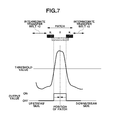
- FIG. 7 illustrates an output waveform detected by the light receiving element 62 b when the patch formed by overlaying the black patches on the yellow patch at the both ends thereof passes through the sensor 60 b .
- the light receiving element 62 b produces only small outputs with respect to the reflection light from the black patches
- the light receiving element 62 b produces a large output with respect to the reflection light from the yellow patch. Therefore, the output waveform rises when the yellow patch is detected after the black patch has passed, and the output waveform falls when the black patch is detected after the yellow patch has passed. Since the black patches are overlaid on the yellow patch at the both ends thereof, the edges acquired from the reflection light from the yellow patch can be regarded as the edges of the black patch. Therefore, a midpoint between these rising edge and falling edge is identified, and this midpoint can be determined as the position of the black patch.
- the patch laid under the black patches is not limited to the yellow patch, and may be formed by any toner that contains a highly diffusely reflective color material such as magenta and cyan. Further, similarly, the position of the black patch can be also detected by forming a patch with yellow patches overlaid on a black patch at both ends thereof. More specifically, in this case, the upwardly protruding output waveform illustrated in FIG. 7 is changed into a downwardly protruding output waveform, and therefore the position of the black patch can be detected by identifying a falling edge, a rising edge, and then a midpoint therebetween. Further, the threshold value for the edge detection may be any value within a range allowing the falling edge and rising edge of the patch to be detected. Individual threshold values may be prepared for the respective toner colors, or a same threshold value may be prepared for all of the toner colors. Further, individual threshold values may be prepared for the respective sensors 60 a and 60 b.
- the method that detects normal reflected light is employed for the sensor 60 a , which is on one side, and the method that detects diffuse reflected light is employed for the sensor 60 b , which is on the other side.
- the mechanism therefor will be described below.
- FIG. 8 illustrates positions of the sensors 60 a and 60 b , and positional deviation correction patterns according to the present exemplary embodiment.
- the sensor 60 a which detects normal reflected light
- the sensor 60 b which detects diffuse reflected light
- the positional deviation correction patterns are formed according to the detection regions of the respective sensors 60 a and 60 b .
- the positional deviation correction patterns to be respectively detected by the sensors 60 a and 60 b are formed as a same pattern by way of example. However, they do not necessarily have to be formed as a same pattern, and the pattern for normal reflected light and the pattern for diffuse reflected light may be formed as different patterns.
- FIG. 9 illustrates details of the patches as the positional deviation correction patterns.
- a positional deviation correction pattern 200 illustrated in FIG. 9 is patches to be detected by the sensor 60 a
- a positional deviation correction pattern 300 illustrated in FIG. 9 is patches to be detected by the sensor 60 b .
- the respective positional deviation correction patterns 200 and 300 are formed as unfixed images so that they do not overlap each other in a direction perpendicular to a direction in which the intermediate transfer belt 10 is conveyed.
- Each of the positional deviation correction patterns 200 and 300 includes yellow patches that have parallelogram shapes directed reversely to each other, magenta patches that have parallelogram shapes directed reversely to each other, cyan patches that have parallelogram shapes directed reversely to each other, and black patches that have parallelogram shapes directed reversely to each other.
- the respective patches are inclined by an angle of 45 degrees from the direction in which the intermediate transfer belt 10 is conveyed. Further, the respective patches are formed in such a manner that, if there is no relative positional deviation amount among them, i.e., a relative positional deviation amount is zero among them, an interval between adjacent patches having parallelogram shapes directed in the same direction becomes equal to an interval between adjacent patches having parallelogram shapes directed in the reverse direction.
- the patch for the black color is formed by overlaying black patches on a yellow patch at both ends thereof, to allow the position of the black patch to be detected even by the sensor 60 b that detects diffuse reflected light. Further, the respective patches are formed so as to have a symmetrical relationship about a reference line illustrated in FIG. 9 . As an example, in FIG.
- the positional deviation correction patterns 200 and 300 are not continuously connected in the direction perpendicular to the direction in which the intermediate transfer belt 10 is conveyed. However, it is not limited thereto, and the positional deviation correction patterns 200 and 300 may be formed so as to be continuously connected in the direction perpendicular to the direction in which the intermediate transfer belt 10 is conveyed.
- a relative temporal deviation rRpym in the sub scanning direction can be calculated according to the following equation (1), assuming that rY1, rM1, rM2, and rY2 represent timings at which ideal positions of patches 201 y , 202 m , 211 m , and 212 y pass through the sensor 60 a from a reference time, respectively.
- rRpym ( rM 1 ⁇ rY 1)+( rM 2 ⁇ rY 2) (1)
- the relative positional deviation amount of the magenta color from the yellow color can be calculated as a distance by multiplying the relative temporal deviation rRpym by the process speed 100 mm/sec.
- the color deviation can be corrected by adjusting the image formation timing of the magenta color by a time corresponding to the relative positional deviation amount of the magenta color, which is acquired as a result of the calculation.
- the relative temporal deviation rRpym in the sub scanning direction is expressed by the following equation (2), assuming that ⁇ rY1, ⁇ rM1, ⁇ rM2, and ⁇ rY2 represent error amounts when the patches 201 y , 202 m , 211 m , and 212 y are detected by the sensor 60 a based on the reference time, respectively.
- the error amounts ⁇ rY1, ⁇ rM1, ⁇ rM2, and ⁇ rY2 correspond to errors generated due to existence of a scratch or a foreign substance at positions corresponding to the patches on the intermediate transfer belt 10 , whereby the possibility of occurrence of the errors increases according to a change on the intermediate transfer belt 10 over time.
- the detection with use of the sensor 60 a results in calculation of a relative positional deviation amount more largely different from the position where the patch is actually formed, as the second term “ ⁇ ( ⁇ rM1 ⁇ rY1)+( ⁇ rM2 ⁇ rY2) ⁇ ” in the equation (2) becomes larger.
- dY1, dM1, dM2, and dY2 represent timings when ideal positions of patches 301 y , 302 m , 311 m , and 312 y pass through the sensor 60 b .
- ⁇ dY1, ⁇ dM1, ⁇ dM2, and ⁇ dY2 represent error amounts from the ideal positions when the respective patches are detected
- a relative positional deviation dRpym in the sub scanning direction that is acquired by the method that detects diffuse reflected light is expressed by the following equation, an equation (3).
- dRpym ⁇ ( dM 1 + ⁇ dM 1) ⁇ ( dY 1+ ⁇ dY 1) ⁇ + ⁇ ( dM 2 + ⁇ dM 2) ⁇ ( dY 2 + ⁇ dY 2) ⁇ (3) Since the error amounts ⁇ dY1, ⁇ dM1, ⁇ dM2, and ⁇ dY2 tend to increase due to reductions in the toner amounts of the patches, they tend to increase according to changes in the toner cartridges over time.
- the relative positional deviation amount in the sub scanning direction may change depending on a position in the width direction of the intermediate transfer belt 10 . Therefore, even if the positional deviation is corrected by a correction of the image formation timing in the sub scanning direction based on the detection result at the position of the sensor on one side, the positional deviation may fail to be appropriately corrected at the position of the sensor on the other side.
- the present exemplary embodiment calculates an average of the detection result produced by the sensor 60 a , which operates according to the method that detects normal reflected light, and the detection result produced by the sensor 60 b , which operates according to the method that detects diffuse reflected light.
- the present exemplary embodiment corrects a positional deviation from an entire image in the sub scanning direction by correcting the image forming timing in the sub scanning direction based on a result of the average calculation.
- a relative positional deviation Rpym is expressed by the following equation, an equation (4).
- the second term “ ⁇ ( ⁇ rM1 ⁇ rY1)+( ⁇ rM2 ⁇ rY2)+( ⁇ dM1 ⁇ dY1)+( ⁇ dM2 ⁇ dY2) ⁇ /2” indicates how large the correction errors are in the results detected by the respective detection methods.
- the one side corresponds to the sensor 60 a that detects normal reflected light, and may produce a detection error due to a scratch, a foreign substance, and the like with a higher probability according to a change on the intermediate transfer belt 10 over time.
- the other side corresponds to the sensor 60 b that detects diffuse reflected light, and tends to have a detection error increasing due to a reduction and unevenness in the toner density according to a change in the toner cartridge over time.
- the present exemplary embodiment uses a plurality of sensors that operate according to different detection methods, and therefore can set a different requirement for generation of a detection error by each of the plurality of sensors. Then, the present exemplary embodiment can correct the positional deviation while reducing an influence of a detection error generated by a specific detection method, by correcting the positional deviation after calculating an average of the detection results produced by the plurality of sensors. In other words, for example, the present exemplary embodiment can reduce the influence of the detection error generated by each sensor to half, by combining the two sensors, the sensor 60 a that operates according to the method that detects normal reflected light and the sensor 60 b that operates according to the method that detects diffuse reflected light.
- the present exemplary embodiment can reduce the influence of the detection error to half by calculating an average of the detection results, compared to an image forming apparatus using two sensors both of which operate according to the method that detects normal reflected light, as described with reference to the above-described equation.
- the present exemplary embodiment can reduce the influence of a change over time, which occurs in the course of use of the image forming apparatus, thereby reducing the deterioration in the accuracy of the positional deviation correction in the method that detects normal reflected light and the method that detects diffuse reflected light.
- the present exemplary embodiment can also correct a positional deviation while reducing a detection error in a similar manner, for not only the positional deviation in the sub scanning direction but also a positional deviation in a main scanning direction.
- a relative positional deviation amount rRsym in the main scanning direction, which is detected by the sensor 60 a can be calculated by the following equation (5).
- Wref_ym represents a reference amount of a relative position in the main scanning direction.
- a relative positional deviation amount dRsym in the main scanning direction which is detected by the sensor 60 b , can be calculated by the following equation, an equation (6).
- dRsym ⁇ ( dM 1 + ⁇ dM 1) ⁇ ( dY 1+ ⁇ dY 1) ⁇ + ⁇ ( dM 2 + ⁇ dM 2) ⁇ ( dY 2 + ⁇ dY 2) ⁇ Wref — ym (6)
- An average value Rsym of the results acquired by the sensors 60 a and 60 b is also calculated to average the relative positional deviation amounts from the entire image in the main scanning direction.
- This average value Rsym is expressed by the following equation, an equation (7).
- Rsym ( rRsym+dRsym )/2 (7)
- the present exemplary embodiment can correct the positional deviation while reducing an influence of a detection error generated by a specific detection method, by correcting the positional deviation after averaging the detection results produced by the plurality of sensors. Accordingly, the present exemplary embodiment can reduce the influence of a change over time, which occurs in the course of use of the image forming apparatus, thereby reducing the deterioration in the accuracy of the positional deviation correction in the method that detects normal reflected light and the method that detects diffuse reflected light.
- FIGS. 10A , 10 B, and 10 C schematically illustrate deviations of the overall magnification and the inclination in the sub scanning direction.
- the overall magnification means a reduction or an increase in an interval between the magenta patches compared to an interval between the yellow patches in the width direction of the intermediate transfer belt 10 .
- FIG. 10A schematically illustrates that the interval between the magenta patches decreases
- FIG. 10B schematically illustrates that the interval between the magenta patches increases.
- the inclination in the sub scanning direction means an offset between the magenta patches compared to an offset between the yellow patches in the sub scanning direction.
- FIG. 10C schematically illustrates that the offset between the magenta patches is larger than the offset between the yellow patches.
- the overall magnification Psy-m and the inclination Ssy-m in the sub scanning direction are a relative positional deviation amount in the main scanning direction and a relative positional deviation amount in the sub scanning direction, which are acquired by the different detection methods, respectively. Therefore, the present exemplary embodiment can correct the positional deviation while reducing an influence of a detection error generated by a specific detection method, by correcting the positional deviation after averaging the detection results produced by the plurality of sensors. Accordingly, the present exemplary embodiment can reduce the influence of a change over time, which occurs in the course of use of the image forming apparatus, thereby reducing the deterioration in the accuracy of the positional deviation correction in the method that detects normal reflected light and the method that detects diffuse reflected light.
- the present exemplary embodiment corrects the positional deviation with use of the sensor 60 a including the single light receiving element 62 a that receives normal reflected light, and the sensor 60 b including the single light receiving element 62 b that receives diffuse reflected light. Therefore, the present exemplary embodiment can reduce the influence of a change over time, which occurs in the course of use of the image forming apparatus, thereby reducing the deterioration in the accuracy of the positional deviation correction in the method that detects normal reflected light and the method that detects diffuse reflected light. Further, the present exemplary embodiment can also prevent cost of the sensor from increasing, because each sensor uses only a single light receiving element therefor.
- a second exemplary embodiment determines the toner amount of the black patch based on a detection result that the sensor 60 a , which operates according to the method that detects normal reflected light, produces by detecting the black patch. Then, the present exemplary embodiment determines whether the positional deviation should be corrected based on a detection result that the sensor 60 b , which operates according to the method that detects diffuse reflected light, produces by detecting the black patch.
- the second exemplary embodiment is characterized by this operation. In the following description, the second exemplary embodiment will be described, omitting detailed descriptions of components and features similar to the above-described exemplary embodiment.
- FIG. 11 illustrates an output waveform that the sensor 60 b produces by detecting patches 308 k , 309 y , and 310 k , when the black patch is formed with a reduced toner amount.
- the black patch is formed with a reduced toner amount, as a result of which the light emitted from the light emitting element 61 b is not absorbed by the black patches 308 k and 310 k , and the diffuse reflected light from the yellow patch 309 y laid under the black patches 308 k and 310 k is received by the light receiving element 62 b .
- the sensor 60 b detects a rise and a fall of the output waveform corresponding to the edges of the yellow patch 309 y . Therefore, the sensor 60 b may identify the position of the black patch by detecting the yellow patch 309 y laid under the black patches 308 k and 310 k , instead of detecting the edges of the black patch.
- the sensor 60 b detects the rising edge and the falling edge affected by the reflection light from the yellow patch laid under the black patches, when the black patch to be detected by the sensor 60 b is formed with a reduced toner amount. Therefore, the position of the patch identified from these edges is different from the position where the black patch is actually located. If the positional deviation is corrected based on the relative positional deviation amount of the black patch different from an actual amount, this correction may result in a further increase in the relative positional deviation amount. Therefore, in this case, the detection result for the correction is not used.
- the light receiving element 62 a of the sensor 60 a which operates according to the method that detects normal reflected light, detects a high output from the intermediate transfer belt 10 , although it little detects the reflection light from the black patch because the infrared light is absorbed by the black patch. Therefore, the sensor 60 a can detect the edges of the black patch. Accordingly, a threshold value for determining that the black patch is formed with a toner amount reduced to less than a predetermined amount can be set, in addition to the threshold value for detecting the intermediate transfer belt 10 and the edges of the black patch.
- the present exemplary embodiment also determines the toner amount of the black patch with use of the sensor 60 a , whereby the positional deviation correction pattern according to the present exemplary embodiment is formed in such a manner that a single patch with no black patch overlaid on any color patch is used as the black patch to be detected by the sensor 60 a , as illustrated in FIG. 12 .
- FIG. 13 illustrates output waveforms that the sensor 60 a produces by detecting the black patch 209 k respectively when the black patch 209 k is formed with a normal toner amount and when the black patch 209 k is formed with a reduced toner amount.
- the output waveform detected by the light receiving element 62 b extends beyond a toner amount detection threshold value set to determine the toner amount of the black patch, whereby the black patch 209 k can be determined to be formed with a predetermined or larger toner amount.
- the output waveform detected by the light receiving element 62 b does not extend beyond the toner amount detection threshold value set to determine the toner amount of the black patch. If the result detected by the sensor 60 a does not extend beyond the toner amount detection threshold value, the black patch formed at the position of the sensor 60 b can be determined to be highly likely formed with a reduced toner amount, too. Therefore, the position of the black patch detected by the sensor 60 b can be determined to be a detection result affected by the yellow patch laid under the black patches.
- the present exemplary embodiment refrains from correcting the positional deviation based on the result detected by the sensor 60 b to prevent the relative positional deviation amount from further largely increasing.
- the present exemplary embodiment refrains from correcting the relative positional deviation amount as processing when determining not to use the detection result that the sensor 60 b produces by detecting the black patch.
- the present exemplary embodiment corrects the relative positional deviation amount only using the result produced by the sensor 60 a .
- the present exemplary embodiment performs control of issuing a request for replacing the black toner cartridge.
- the present exemplary embodiment determines the toner amount of the black patch based on the detection result that the sensor 60 a , which operates according to the method that detects normal reflected light, produces by detecting the black patch. Then, the present exemplary embodiment determines whether to correct the positional deviation based on the detection result that the sensor 60 b , which operates according to the method that detects diffuse reflected light, produces by detecting the black patch. As a result, if the toner amount of the black patch is determined to be smaller than the predetermined amount, the present exemplary embodiment refrains from correcting the positional deviation based on the result detected by the sensor 60 b , thereby succeeding in preventing the relative positional deviation amount from further largely increasing.
- the black patch to be detected by the sensor 60 a by way of example, but it is not limited thereto.
- another black patch than the positional deviation correction pattern may be formed as a toner amount determination patch for determining the toner amount of the black patch.
- each sensor emits the light from a bullet-shaped LED, and receives the light by a bullet-shaped phototransistor.
- a third exemplary embodiment will be described as an example that performs control for correcting the positional deviation with use of a sensor that emits the light from a chip-type LED.
- the third exemplary embodiment will be described, omitting detailed descriptions of components and features similar to the above-described exemplary embodiments.
- FIGS. 14A and 14B are cross-sectional views of a sensor 170 a and a sensor 170 b , respectively.
- the sensor 170 a detects normal reflected light from the intermediate transfer belt 10 or a patch 1234 .
- a chip LED 171 a and a chip light receiving element 172 a are mounted on a circuit substrate 1262 , and are soldered thereon.
- a housing 1265 defines light guide paths of the respective chip LED 171 a and chip light receiving element 172 a .
- the chip LED 171 a and the chip light receiving element 172 a are disposed in such a manner that central lines 1267 and 1266 of the respective light paths define angles of 15 degrees from a direction 1268 perpendicular to the intermediate transfer belt 10 symmetrically about the direction 1268 .
- the chip LED 171 a and the chip light receiving element 172 a are disposed in this manner, by which direct reflection light (normal reflected light) reflected by the intermediate transfer belt 10 or the patch 1234 can be introduced into the light guide path on the light receiving side as efficient as possible in a similar manner to the above-described first exemplary embodiment.
- a chip-type phototransistor or the like can be used as the chip light receiving element 172 a , and it is possible to reduce the size of the light receiving element 172 a compared to the lamp-type phototransistor.
- the sensor 170 b detects diffuse reflected light (irregular reflected light) from a patch 1235 .
- a chip LED 171 b and a chip light receiving element 172 b are mounted on a circuit substrate, and are soldered thereon.
- a housing 1277 defines light guide paths of the respective chip LED 171 b and chip light receiving element 172 b .
- the chip LED 171 b is disposed in such a manner that a central line 1275 of the light path on the light emitting side has an angle of 15 degrees from a direction 1274 perpendicular to the intermediate transfer belt 10 .
- the chip light receiving element 172 b is disposed in such a manner that a central line 1276 of the light path on the light receiving side has an angle of 45 degrees from the direction 1274 perpendicular to the intermediate transfer belt 10 .
- the chip LED 171 a and the chip light receiving element 172 b are disposed in this manner, by which the direct reflection light from the intermediate transfer belt 10 is prevented from being introduced into the light guide path on the light receiving side as much as possible in a similar manner to the above-described first exemplary embodiment.
- the present exemplary embodiment has been described assuming that the sensor 170 a receives normal reflected light and the sensor 170 b receives diffuse reflected light by way of example, but is not limited thereto.
- the present exemplary embodiment may be configured in such a manner that the sensor 170 a receives diffuse reflected light and the sensor 170 b receives normal reflected light. Further, it can be also said that the chip light receiving element 172 a of the sensor 170 a is arranged so as to be located in a direction in which the light emitted from the chip LED 171 a is specularly reflected, among directions in which this light is reflected. On the other hand, it can be also said that the chip light receiving element 172 b of the sensor 170 b is arranged so as to be located in a different direction from a direction in which the light emitted from the chip LED 171 b is specularly reflected, among directions in which this light is reflected.
- FIGS. 14A and 14B employ resin mold-type optical elements for the LEDs 171 a and 171 b as the light emitting elements, and the light receiving elements (phototransistors or photodiodes) 172 a and 172 b .
- These configurations are characterized in that they include a lead frame so as to allow each of the light emitting element and the light receiving element to be turned in a different direction freely to some degree through a change in an angle at which the lead frame is bent, thereby improving flexibility in terms of an angle and a position at which each of the light emitting element and the light receiving element is arranged.
- an optically characteristically excellent direction for example, a direction of the LED that can emit the light with a high intensity, and a direction of the light receiving element that is highly sensitive to the light
- the presence of the lead frame leads to a certain volume from the light emitting element or the light receiving element to the circuit substrate, thereby resulting in a slight increase in the size of the sensor as a whole.
- sensors illustrated in FIGS. 15A and 15B can be also used in consideration of a reduction in the size of the sensor.
- the sensors illustrated in FIGS. 15A and 15B employ surface mount-type optical elements, in which a chip is directly mounted on a surface of a circuit substrate, with no lead frame used therein, thereby realizing a size reduction compared to the sensors 170 a and 170 b illustrated in FIGS. 14A and 14B .
- the optically characteristically excellent direction is a direction perpendicular to the surface on which the optical element is mounted.
- the LED emits the light with a lower intensity, and the light receiving element becomes less sensitive to the light, according to an increase in an angle of the light path from the direction perpendicular to the surface on which the optical element is mounted.
- the optical elements are disposed in consideration of this characteristic.
- the sensor 180 a is a sensor that detects normal reflected light from the intermediate transfer belt 10 or the patch 1234 , and is configured in a similar manner to the above-described sensor 170 a illustrated in FIG. 14A . Therefore, a detailed description thereof will be omitted here.
- the sensor 180 b detects diffuse reflected light from the patch 1235 .
- the light guide path of the optical element may be aligned with the direction perpendicular to the surface on which the light emitting or receiving element is mounted as close as possible, to improve the light emission intensity or the light receiving sensitivity.
- an LED 181 b as the light emitting element is disposed in such a manner that a central line of a light path thereof is in alignment with a direction 1353 perpendicular to the intermediate transfer belt 10 .
- a light receiving element 182 b is disposed in such a manner that a central line of a light guide path thereof has an angle of 20 degrees from the direction 1353 perpendicular to the intermediate transfer belt 10 .
- the sensor 180 b is configured in this manner, by which the light emitting element can emit the light with an improved intensity.
- the light guide path on the light receiving side is located close to a reflection region of the normal reflected light from the intermediate transfer belt 10 , whereby the normal reflected light from the intermediate transfer belt 10 may be partially introduced into the light receiving side.
- the senor 180 b can be configured in such a manner that the LED 181 b is disposed with the central line of the light path thereof defining an angle of 20 degrees from the direction 1353 perpendicular to the intermediate transfer belt 10 , and the light receiving element 182 b is disposed with the central line of the light path thereof in alignment with the direction 1353 perpendicular to the intermediate transfer belt 10 .
- the exemplary embodiment When detecting a patch, the sensor 180 a illustrated in FIG. 15A , which operates according to the method that detects normal reflected light, produces an output waveform as illustrated in FIG. 5 . Since the light receiving element 182 a mainly detects normal reflected light, the sensor 180 a can produce a high output with respect to the reflection light from the intermediate transfer belt 10 while producing a low output with respect to the reflection light from a chromatic patch. Therefore, the present exemplary embodiment can detect edges of the patch at both ends thereof according to changes beyond a preset edge threshold value in an output when detecting the chromatic patch, thereby identifying the position of the patch from the edges at the both ends.
- the senor 180 b illustrated in FIG. 15B which operates according to the method that detects diffuse reflected light, produces an output waveform as illustrated in FIG. 6 . Since the light receiving element 182 b mainly detects diffuse reflected light, the sensor 180 b produces a low output with respect to the reflection light from the intermediate transfer belt 10 while producing a high output with respect to the reflection light from the chromatic patch. Therefore, the present exemplary embodiment can detect edges of the patch at both ends thereof according to changes beyond a preset edge threshold value in an output when detecting the chromatic patch, thereby identifying the position of the patch from the edges at the both ends.
- the black patch absorbs the infrared light emitted from the LED 181 b , and therefore cannot be distinguished from the intermediate transfer belt 10 . Therefore, in the present exemplary embodiment, the patch for the black color is also formed by overlaying black patches on a yellow patch at both ends of the yellow patch. The output waveform produced at this time is as illustrated in FIG. 7 . The present exemplary embodiment can estimate that edges of the black patch are detected according to changes beyond the edge threshold value in an output when the light receiving element 182 b detects the reflection light from the yellow patch, thereby identifying the position of the black patch from the edges at the both ends.
- the present exemplary embodiment can acquire the relative positional deviation amounts in the sub scanning direction and the main scanning direction, the overall magnification, and the inclination in the sub scanning direction by calculating the distance between the patches of the respective colors. Further, the present exemplary embodiment corrects the positional deviation based on the detection results output from both the sensor 180 a , which operates according to the method that detects normal reflected light, and the sensor 180 b , which operates according to the method that detects diffuse reflected light, in a similar manner to the above-described first exemplary embodiment.
- the present exemplary embodiment can reduce the influence of a change over time, which occurs in the course of use of the image forming apparatus, thereby reducing the deterioration in the accuracy of the positional deviation correction in the method that detects normal reflected light and the method that detects diffuse reflected light.
- a dynamic range between an output detected from a solid image and an output detected when the toner amount is zero may be maximized, to allow the patch output detected by the sensor 180 a or 180 b to stably fall below or exceed the edge threshold value. Since the sensor 180 b is configured in such a manner that only the small angle of 20 degrees is defined between the light patch axis of the LED 181 b and the light path axis of the light receiving element 182 b so that the normal reflected light is partially incident on the light receiving element 182 b , thereby reducing the dynamic range compared to a sensor having an angle larger than 20 degrees. However, the present exemplary embodiment can be carried out by preparing 1.0 V or higher as an absolute value of the dynamic range, or by preparing 1.5 V or higher.
- the present exemplary embodiment can reduce the influence of a change over time, which occurs in the course of use of the image forming apparatus, thereby reducing the deterioration in the accuracy of the positional deviation correction in the method that detects normal reflected light and the method that detects diffuse reflected light.
- the rotating member on which the positional deviation correction patterns are formed may be any member that allows the formed positional deviation correction patterns to be detected, such as the photosensitive drum 1 and an electrostatic conveyance belt that conveys the recording material P.
- the configuration of the present invention it is possible to reduce the deterioration in the accuracy of the positional deviation correction in the method that detects normal reflected light and the method that detects diffuse reflected light.
Landscapes
- Physics & Mathematics (AREA)
- General Physics & Mathematics (AREA)
- Engineering & Computer Science (AREA)
- Microelectronics & Electronic Packaging (AREA)
- Control Or Security For Electrophotography (AREA)
- Color Electrophotography (AREA)
Abstract
Description
rRpym=(rM1−rY1)+(rM2−rY2) (1)
According to the equation (1), (rM1−rY1)=(rY2−rM2) when rRpym=0.
rRpym={(rM1+ΔrM1)−(rY1+ΔrY1)}+{(rM2+ΔrM2)−(rY2+ΔrY2)}={(rM1−rY1)+(rM2−rY2)}+{(ΔrM1−ΔrY1)+(ΔrM2−ΔrY2)} (2)
The error amounts ΔrY1, ΔrM1, ΔrM2, and ΔrY2 correspond to errors generated due to existence of a scratch or a foreign substance at positions corresponding to the patches on the
dRpym={(dM1+ΔdM1)−(dY1+ΔdY1)}+{(dM2+ΔdM2)−(dY2+ΔdY2)} (3)
Since the error amounts ΔdY1, ΔdM1, ΔdM2, and ΔdY2 tend to increase due to reductions in the toner amounts of the patches, they tend to increase according to changes in the toner cartridges over time.
Rpym=(rRpym+dRpym)/2=[{(rM1+ΔrM1)−(rY1+ΔrY1)}+{(rM2+ΔrM2)−(rY2+ΔrY2)}+{(dM1+ΔdM1)−(dY1+ΔdY1)}+{(dM2+ΔdM2)−(dY2+ΔdY2)}]/2
={(rM1−rY1)+(rM2−rY2)+(dM1−dY1)+(dM2−dY2)}/2+{(ΔrM1−ΔrY1)+(ΔrM2−ΔrY2)+(ΔdM1−ΔdY1)+(ΔdM2−ΔdY2)}/2 (4)
rRsym={(rM1+ΔrM1)−(rY1+ΔrY1)}−{(rM2+ΔrM2)−(rY2+ΔrY2)}−Wref — ym
={(rM1−rY1)−(rM2−rY2)}+{(ΔrM1−ΔrY1)−(ΔrM2−ΔrY2)}−Wref — ym (5)
dRsym={(dM1+ΔdM1)−(dY1+ΔdY1)}+{(dM2+ΔdM2)−(dY2+ΔdY2)}−Wref — ym (6)
Rsym=(rRsym+dRsym)/2 (7)
Psy-m=(W1/S1)×(rRsym−dRsym)/2 (8)
Ssy-m=(W1/S1)×(rRpym−dRpym)/2 (9)
In the equations (8) and (9), W1 represents a length of the recording material P in the width direction, and S1 represents an interval between the
Claims (19)
Applications Claiming Priority (2)
| Application Number | Priority Date | Filing Date | Title |
|---|---|---|---|
| JP2013-188450 | 2013-09-11 | ||
| JP2013188450A JP6282068B2 (en) | 2013-09-11 | 2013-09-11 | Image forming apparatus, misregistration detection apparatus, and misregistration detection method |
Publications (2)
| Publication Number | Publication Date |
|---|---|
| US20150071687A1 US20150071687A1 (en) | 2015-03-12 |
| US9274448B2 true US9274448B2 (en) | 2016-03-01 |
Family
ID=52625765
Family Applications (1)
| Application Number | Title | Priority Date | Filing Date |
|---|---|---|---|
| US14/480,428 Active US9274448B2 (en) | 2013-09-11 | 2014-09-08 | Image forming apparatus, positional deviation detection apparatus, and positional deviation detection method |
Country Status (2)
| Country | Link |
|---|---|
| US (1) | US9274448B2 (en) |
| JP (1) | JP6282068B2 (en) |
Families Citing this family (2)
| Publication number | Priority date | Publication date | Assignee | Title |
|---|---|---|---|---|
| JP6048449B2 (en) * | 2014-05-29 | 2016-12-21 | コニカミノルタ株式会社 | Image forming apparatus |
| JP7001044B2 (en) * | 2018-11-28 | 2022-01-19 | オムロン株式会社 | Control system |
Citations (9)
| Publication number | Priority date | Publication date | Assignee | Title |
|---|---|---|---|---|
| JP2001318501A (en) | 2000-05-12 | 2001-11-16 | Canon Inc | Image forming apparatus and color misregistration detection processing method of image forming apparatus |
| US20090080915A1 (en) * | 2007-09-21 | 2009-03-26 | Canon Kabushiki Kaisha | Color image forming apparatus and color misregistration correction method therefor |
| JP2009223248A (en) | 2008-03-19 | 2009-10-01 | Ricoh Co Ltd | Color image forming apparatus |
| US20110229820A1 (en) * | 2010-03-18 | 2011-09-22 | Higa Takuma | Image forming apparatus |
| US20110280633A1 (en) * | 2010-05-17 | 2011-11-17 | Canon Kabushiki Kaisha | Image forming apparatus |
| US20110318065A1 (en) * | 2010-06-29 | 2011-12-29 | Ricoh Company, Ltd. | Apparatus and method of color shift correction, and medium storing color shift correction program |
| JP2012027140A (en) | 2010-07-21 | 2012-02-09 | Fuji Xerox Co Ltd | Image forming device and image detection device |
| JP2012237904A (en) | 2011-05-12 | 2012-12-06 | Canon Inc | Image forming device |
| US20130259496A1 (en) * | 2012-04-02 | 2013-10-03 | Konica Minolta Business Technologies, Inc. | Image forming apparatus |
Family Cites Families (5)
| Publication number | Priority date | Publication date | Assignee | Title |
|---|---|---|---|---|
| JP2002202651A (en) * | 2000-12-28 | 2002-07-19 | Casio Electronics Co Ltd | Apparatus and method for adjusting color image forming position and recording medium on which program is recorded |
| JP2005070117A (en) * | 2003-08-26 | 2005-03-17 | Sharp Corp | Image forming apparatus and color misregistration correction method for image forming apparatus |
| JP4478669B2 (en) * | 2005-08-31 | 2010-06-09 | キヤノン株式会社 | Sensor and recording apparatus using the same |
| JP2007156159A (en) * | 2005-12-06 | 2007-06-21 | Fuji Xerox Co Ltd | Color shift detection sensor and color shift detecting device |
| JP2010256118A (en) * | 2009-04-23 | 2010-11-11 | Ricoh Co Ltd | Reflection type photosensor, image forming apparatus, and reflection type photosensor assembly method |
-
2013
- 2013-09-11 JP JP2013188450A patent/JP6282068B2/en not_active Expired - Fee Related
-
2014
- 2014-09-08 US US14/480,428 patent/US9274448B2/en active Active
Patent Citations (9)
| Publication number | Priority date | Publication date | Assignee | Title |
|---|---|---|---|---|
| JP2001318501A (en) | 2000-05-12 | 2001-11-16 | Canon Inc | Image forming apparatus and color misregistration detection processing method of image forming apparatus |
| US20090080915A1 (en) * | 2007-09-21 | 2009-03-26 | Canon Kabushiki Kaisha | Color image forming apparatus and color misregistration correction method therefor |
| JP2009223248A (en) | 2008-03-19 | 2009-10-01 | Ricoh Co Ltd | Color image forming apparatus |
| US20110229820A1 (en) * | 2010-03-18 | 2011-09-22 | Higa Takuma | Image forming apparatus |
| US20110280633A1 (en) * | 2010-05-17 | 2011-11-17 | Canon Kabushiki Kaisha | Image forming apparatus |
| US20110318065A1 (en) * | 2010-06-29 | 2011-12-29 | Ricoh Company, Ltd. | Apparatus and method of color shift correction, and medium storing color shift correction program |
| JP2012027140A (en) | 2010-07-21 | 2012-02-09 | Fuji Xerox Co Ltd | Image forming device and image detection device |
| JP2012237904A (en) | 2011-05-12 | 2012-12-06 | Canon Inc | Image forming device |
| US20130259496A1 (en) * | 2012-04-02 | 2013-10-03 | Konica Minolta Business Technologies, Inc. | Image forming apparatus |
Also Published As
| Publication number | Publication date |
|---|---|
| US20150071687A1 (en) | 2015-03-12 |
| JP6282068B2 (en) | 2018-02-21 |
| JP2015055730A (en) | 2015-03-23 |
Similar Documents
| Publication | Publication Date | Title |
|---|---|---|
| US8995892B2 (en) | Image forming apparatus with threshold adjustment for superposed measurement images | |
| WO2013121767A1 (en) | Optical sensor, and image formation device | |
| US9977361B2 (en) | Image forming apparatus and image forming system | |
| US9170516B2 (en) | Image forming apparatus and image forming method | |
| US9304083B2 (en) | Optical detection device and image forming apparatus including the same | |
| US11754940B2 (en) | Image forming apparatus | |
| US9164454B2 (en) | Image forming apparatus for performing registration and density correction control | |
| US20130302049A1 (en) | Image forming apparatus for storing sampling values and method therefor | |
| CN102004411A (en) | Image forming apparatus and detecting method of pattern image regarding image quality adjustment | |
| US8649718B2 (en) | Apparatus and method of color shift correction, and medium storing color shift correction program | |
| US9170544B2 (en) | Image forming apparatus | |
| JP2011133845A (en) | Image forming apparatus | |
| JP6366331B2 (en) | Image forming apparatus | |
| US9274448B2 (en) | Image forming apparatus, positional deviation detection apparatus, and positional deviation detection method | |
| JP6675344B2 (en) | Optical sensor and image forming apparatus | |
| US9880497B2 (en) | Image forming device, position shift correction method, and recording medium | |
| US9625865B2 (en) | Image forming apparatus and control method for image forming apparatus | |
| JP5106841B2 (en) | Image forming apparatus | |
| CN103901753B (en) | Image processing system | |
| JP2008040441A (en) | Image forming apparatus | |
| JP5636780B2 (en) | Image forming apparatus | |
| JP2012027140A (en) | Image forming device and image detection device | |
| US8150302B2 (en) | Image forming apparatus and image forming method that detects an amount of color misalignment using reflected light | |
| JP2016090927A (en) | Image forming apparatus | |
| US9946209B2 (en) | Image forming apparatus |
Legal Events
| Date | Code | Title | Description |
|---|---|---|---|
| AS | Assignment |
Owner name: CANON KABUSHIKI KAISHA, JAPAN Free format text: ASSIGNMENT OF ASSIGNORS INTEREST;ASSIGNORS:ISHIZUMI, KEISUKE;NAKAGAWA, KEN;KOBAYASHI, SHINSUKE;SIGNING DATES FROM 20140821 TO 20140822;REEL/FRAME:034955/0529 |
|
| STCF | Information on status: patent grant |
Free format text: PATENTED CASE |
|
| MAFP | Maintenance fee payment |
Free format text: PAYMENT OF MAINTENANCE FEE, 4TH YEAR, LARGE ENTITY (ORIGINAL EVENT CODE: M1551); ENTITY STATUS OF PATENT OWNER: LARGE ENTITY Year of fee payment: 4 |
|
| MAFP | Maintenance fee payment |
Free format text: PAYMENT OF MAINTENANCE FEE, 8TH YEAR, LARGE ENTITY (ORIGINAL EVENT CODE: M1552); ENTITY STATUS OF PATENT OWNER: LARGE ENTITY Year of fee payment: 8 |