JP6675344B2 - Optical sensor and image forming apparatus - Google Patents
Optical sensor and image forming apparatus Download PDFInfo
- Publication number
- JP6675344B2 JP6675344B2 JP2017044224A JP2017044224A JP6675344B2 JP 6675344 B2 JP6675344 B2 JP 6675344B2 JP 2017044224 A JP2017044224 A JP 2017044224A JP 2017044224 A JP2017044224 A JP 2017044224A JP 6675344 B2 JP6675344 B2 JP 6675344B2
- Authority
- JP
- Japan
- Prior art keywords
- light
- light receiving
- receiving element
- image
- irradiation
- Prior art date
- Legal status (The legal status is an assumption and is not a legal conclusion. Google has not performed a legal analysis and makes no representation as to the accuracy of the status listed.)
- Active
Links
- 230000003287 optical effect Effects 0.000 title claims description 98
- 238000001514 detection method Methods 0.000 claims description 169
- 238000012937 correction Methods 0.000 claims description 40
- 230000015572 biosynthetic process Effects 0.000 claims description 5
- 230000004044 response Effects 0.000 claims description 5
- 230000001678 irradiating effect Effects 0.000 claims description 2
- 230000000903 blocking effect Effects 0.000 claims 3
- 230000001105 regulatory effect Effects 0.000 claims 2
- 230000001276 controlling effect Effects 0.000 claims 1
- 238000012546 transfer Methods 0.000 description 138
- 238000012360 testing method Methods 0.000 description 78
- 230000001788 irregular Effects 0.000 description 42
- 230000000052 comparative effect Effects 0.000 description 32
- 238000000034 method Methods 0.000 description 17
- 230000032258 transport Effects 0.000 description 12
- 238000010586 diagram Methods 0.000 description 11
- 239000003086 colorant Substances 0.000 description 10
- 238000006073 displacement reaction Methods 0.000 description 10
- 238000005259 measurement Methods 0.000 description 10
- 230000002093 peripheral effect Effects 0.000 description 10
- 238000003708 edge detection Methods 0.000 description 8
- 230000007423 decrease Effects 0.000 description 6
- 230000003068 static effect Effects 0.000 description 5
- 238000004140 cleaning Methods 0.000 description 4
- 239000000463 material Substances 0.000 description 4
- 239000002699 waste material Substances 0.000 description 4
- 230000007547 defect Effects 0.000 description 3
- 230000000694 effects Effects 0.000 description 3
- 238000012545 processing Methods 0.000 description 3
- 230000035945 sensitivity Effects 0.000 description 2
- 238000000926 separation method Methods 0.000 description 2
- 239000000758 substrate Substances 0.000 description 2
- XAGFODPZIPBFFR-UHFFFAOYSA-N aluminium Chemical compound [Al] XAGFODPZIPBFFR-UHFFFAOYSA-N 0.000 description 1
- 229910052782 aluminium Inorganic materials 0.000 description 1
- 238000006243 chemical reaction Methods 0.000 description 1
- 230000001419 dependent effect Effects 0.000 description 1
- 230000002542 deteriorative effect Effects 0.000 description 1
- 238000005516 engineering process Methods 0.000 description 1
- 238000010438 heat treatment Methods 0.000 description 1
- 239000011347 resin Substances 0.000 description 1
- 229920005989 resin Polymers 0.000 description 1
- 239000004065 semiconductor Substances 0.000 description 1
- 239000007787 solid Substances 0.000 description 1
Images


Landscapes
- Investigating Or Analysing Materials By Optical Means (AREA)
- Color Electrophotography (AREA)
- Photo Coupler, Interrupter, Optical-To-Optical Conversion Devices (AREA)
Description
本発明は、発光素子から出射した光の正反射光及び乱反射光を複数の受光素子で受光して検出対象を検出するための光学センサ、及び当該光学センサを備えた画像形成装置に関するものである。 The present invention relates to an optical sensor for detecting specularly reflected light and irregularly reflected light of light emitted from a light emitting element with a plurality of light receiving elements to detect a detection target, and an image forming apparatus including the optical sensor. .
近年、電子写真方式の画像形成装置は、印刷スピードの高速化のために、感光体を色ごとに設けた構成であるタンデム型が主流となっている。タンデム型の画像形成装置では、例えば中間転写ベルトに色ずれ量の検出のためのテストパターンである検出用画像(トナー像)を形成し、当該検出用画像に光を照射してその反射光を光学センサで検出することで、色ずれ量を判定している。また、このような光学センサを用いてトナーの濃度(画像の濃度)の判定も行われている。特許文献1には、トナー像に照射した光の正反射光と乱反射光とをそれぞれ個別の受光部(センサ)で受光し、受光光量に基づいてトナーの濃度を検出する技術が開示されている。このような技術によれば、画像形成装置で用いる複数色のトナーが、光学センサによって使用される光に対して異なる反射特性を有する場合にも、光学センサによるトナーの検出精度を向上させることが可能である。 2. Description of the Related Art In recent years, in order to increase the printing speed, an electrophotographic image forming apparatus is mainly of a tandem type in which a photoconductor is provided for each color. In a tandem-type image forming apparatus, for example, a detection image (toner image), which is a test pattern for detecting a color shift amount, is formed on an intermediate transfer belt, and the detection image is irradiated with light to reflect reflected light. The color misregistration amount is determined by detecting with the optical sensor. The determination of the toner density (image density) is also performed using such an optical sensor. Patent Literature 1 discloses a technique in which specularly reflected light and irregularly reflected light of light applied to a toner image are received by individual light receiving units (sensors), and the toner density is detected based on the amount of received light. . According to such a technique, it is possible to improve the detection accuracy of the toner by the optical sensor even when the multi-color toner used in the image forming apparatus has different reflection characteristics with respect to the light used by the optical sensor. It is possible.
上述のタイプの光学センサでは、一般に、発光素子が出射する光を制限する(絞り込む)ための絞りが設けられるとともに、正反射光と乱反射光とを分離するために、正反射光及び乱反射光をそれぞれ受光する受光素子に対してもそのような絞りが設けられる。そのような光学センサとして、特許文献2,3には、回路基板の表面に光学素子を直接実装する表面実装タイプの光学センサが開示されている。
In an optical sensor of the type described above, a stop for restricting (stopping) light emitted from a light emitting element is generally provided, and specular reflected light and diffuse reflected light are separated in order to separate specular reflected light and diffuse reflected light. Such a stop is also provided for the light receiving element that receives light. As such an optical sensor,
特許文献2では、発光素子及び2個の受光素子が直接実装された回路基板に対して光学ユニットホルダを取り付けるとともに、光学ユニットホルダの外表面に、発光素子及び2個の受光素子のそれぞれに対応する3個の偏光フィルタを配置している。しかし、このように複数の偏光フィルタを用いると、装置のコストアップ及び生産性の低下につながりうる。一方、特許文献3では、各光学素子(発光素子及び2個の受光素子)に対応する絞りとして機能する開口部(導光路)を有するハウジングを、開口部を構成する遮光壁が、回路基板に設けられたスリット穴に挿入されるように構成している。これにより、各光学素子を回路基板の表面に実装した光学センサにおける遮光性を向上させている。
In
しかし、特許文献3に示される光学センサでは、遮光性を向上させたハウジングを実現するために、発光素子及び2個の受光素子を、互いにある程度の距離を置いて配置する必要がある。このような光学センサの構成によれば、遮光性の向上は可能であっても、発光素子及び2個の受光素子が並べられた方向における光学センサのサイズが大きくなる。このため、光学センサにおける更なる小型化の実現が望まれる。
However, in the optical sensor disclosed in
本発明は、上述の問題に鑑みてなされたものである。本発明は、発光素子が出射した光の正反射光及び乱反射光をそれぞれ異なる受光素子で受光して検出対象を検出するための光学センサの小型化を可能にする技術を提供することを目的とする。 The present invention has been made in view of the above problems. An object of the present invention is to provide a technology that enables downsizing of an optical sensor for detecting a detection target by receiving specularly reflected light and irregularly reflected light of light emitted from a light emitting element with different light receiving elements. I do.
本発明は、例えば、光学センサとして実現できる。本発明の一態様に係る光学センサは、被照射体に向けて照射光を照射する発光素子と、前記照射光が前記被照射体の照射領域で乱反射された乱反射光を受光するための第1受光素子と、前記照射光が前記被照射体の前記照射領域で正反射された正反射光を受光するための第2受光素子と、を備え、前記第1受光素子は、前記照射領域のうち、第1領域で乱反射した前記乱反射光を受光し、前記第2受光素子は、主走査方向において少なくとも一部は前記第1領域を含まない第2領域で正反射した前記正反射光を受光することを特徴とする。 The present invention can be realized, for example, as an optical sensor. An optical sensor according to one embodiment of the present invention includes a light-emitting element that irradiates irradiation light toward an irradiation target, and a first light-emitting element that receives diffused reflection light in which the irradiation light is irregularly reflected in an irradiation region of the irradiation target. A light receiving element, and a second light receiving element for receiving the specularly reflected light in which the irradiation light is regularly reflected in the irradiation area of the irradiation object, wherein the first light receiving element is included in the irradiation area. Receiving the irregularly reflected light irregularly reflected in the first area, and the second light receiving element receives the regular reflected light at least partially reflected in the second area not including the first area in the main scanning direction. It is characterized by the following.
本発明の他の一態様に係る光学センサは、被照射体に向けて照射光を照射する発光素子と、前記照射光が前記被照射体の照射領域で乱反射された乱反射光を受光するための第1受光素子と、前記照射光が前記被照射体の前記照射領域で正反射された正反射光を受光するための第2受光素子と、前記発光素子から出射された光を前記被照射体に向けて導くための第1開口と、前記照射領域のうち、第1領域で乱反射した前記乱反射光を前記第1受光素子に導くための第2開口と、主走査方向において少なくとも一部は前記第1領域を含まない第2領域で正反射した前記正反射光を前記第2受光素子に導く第3開口と、を形成するハウジングと、を備えることを特徴とする。 An optical sensor according to another embodiment of the present invention is a light-emitting element that irradiates irradiation light toward an irradiation target, and receives light that is irregularly reflected by the irradiation light in an irradiation region of the irradiation target. A first light receiving element, a second light receiving element for receiving regular reflection light in which the irradiation light is regularly reflected in the irradiation area of the irradiation object, and light emitted from the light emitting element to the irradiation object. And a second opening for guiding the diffusely reflected light irregularly reflected in the first region to the first light receiving element in the irradiation area, and at least a part in the main scanning direction. And a third opening for guiding the specularly reflected light that is specularly reflected by the second region that does not include the first region to the second light receiving element .
本発明によれば、発光素子から出射した光の正反射光及び乱反射光をそれぞれ異なる受光素子で受光して検出対象を検出するための光学センサの小型化が可能になる。 Advantageous Effects of Invention According to the present invention, it is possible to reduce the size of an optical sensor for detecting a detection target by receiving specularly reflected light and irregularly reflected light of light emitted from a light emitting element with different light receiving elements.
以下、本発明を実施するための形態について図面を用いて説明する。なお、以下の実施形態は特許請求の範囲に係る発明を限定するものでなく、また実施形態で説明されている特徴の組み合わせの全てが発明の解決手段に必須のものとは限らない。 Hereinafter, embodiments for carrying out the present invention will be described with reference to the drawings. It should be noted that the following embodiments do not limit the invention according to the claims, and not all combinations of the features described in the embodiments are necessarily essential to the means for solving the invention.
[第1実施形態]
<画像形成装置の概要>
図1は、第1実施形態に係る画像形成装置100のハードウェア構成例を示す断面図である。本実施形態の画像形成装置100は、イエロー(Y)、マゼンタ(M)、シアン(C)及びブラック(K)の現像剤(トナー)によってマルチカラー画像を形成するカラーレーザプリンタである。画像形成装置100は、例えば、印刷装置、プリンタ、複写機、複合機(MFP)及びファクシミリ装置のいずれであってもよい。なお、参照符号の末尾のY,M,C,Kは、それぞれ、対応する部材が対象とする現像剤(トナー)の色が、イエロー、マゼンタ、シアン、ブラックであることを示している。以下の説明では、色を区別する必要がない場合には、末尾のY,M,C,Kを省いた参照符号を使用する。
[First Embodiment]
<Overview of Image Forming Apparatus>
FIG. 1 is a cross-sectional view illustrating a hardware configuration example of the
画像形成装置100は、それぞれY,M,C,Kの画像を形成する画像形成ステーションに対応する4個のプロセスカートリッジ7(プロセスカートリッジ7Y,7M,7C,7K)を備えている。図1では、Yに対応するプロセスカートリッジ7Yの構成部品にのみ参照番号を付与しているものの、4個のプロセスカートリッジ7Y,7M,7C,7Kは、同一の構成を採用している。ただし、4個のプロセスカートリッジ7Y,7M,7C,7Kは、それぞれ異なる色(Y,M,C,K)のトナーによって画像を形成する点で相違している。
The
感光ドラム1の周囲には、その回転方向に沿って順に、帯電ローラ2、露光ユニット3、現像ユニット4、一次転写ローラ26、及びクリーニングブレード8が配置されている。本実施形態では、感光ドラム1、帯電ローラ2、現像ユニット4及びクリーニングブレード8は、画像形成装置100に対して着脱可能なプロセスカートリッジ7として一体化されている。露光ユニット3は、プロセスカートリッジ7の鉛直方向下方に配置されている。
Around the photosensitive drum 1, a
プロセスカートリッジ7は、現像ユニット4及びクリーナユニット5によって構成されている。現像ユニット4は、現像ローラ24、現像剤塗布ローラ25、及びトナー容器を有している。トナー容器には、対応する色のトナーが収納されている。現像ローラ24は、駆動モータ(図示せず)によって回転駆動され、高圧電源44(図2)から現像バイアス電圧が印加されることで、トナー容器に収納されたトナーによって静電潜像の現像を行う。クリーナユニット5は、感光ドラム1、帯電ローラ2、クリーニングブレード8、及び廃トナー容器を有している。
The process cartridge 7 includes a developing unit 4 and a cleaner unit 5. The developing unit 4 includes a developing
感光ドラム1は、アルミニウム製シリンダの外周面に有機光導伝体層(OPC)を塗布して構成したものである。感光ドラム1は、その両端部がフランジによって回転自在に支持されており、一方の端部に駆動モータ(図示せず)から駆動力が伝達されることによって、図1に示す矢印の方向に回転駆動される。帯電ローラ2は、感光ドラム1の表面を一様に所定の電位に帯電させる。露光ユニット3は、画像情報(画像信号)に基づいて、感光ドラム1にレーザビームを照射して感光ドラム1を露光することで、感光ドラム1上に静電潜像を形成する。現像ユニット4は、感光ドラム1上の静電潜像にトナーを付着させて当該静電潜像を現像することによって、感光ドラム1上にトナー像(トナー画像)を形成する。
The photosensitive drum 1 is formed by applying an organic photoconductor layer (OPC) to an outer peripheral surface of an aluminum cylinder. The photosensitive drum 1 is rotatably supported at both ends by flanges. When a driving force is transmitted from one end to a driving motor (not shown), the photosensitive drum 1 rotates in the direction of the arrow shown in FIG. Driven. The charging
中間転写ベルト12a、駆動ローラ12b、及びテンションローラ12cは、中間転写ユニット12を構成している。中間転写ベルト12aは、駆動ローラ12bとテンションローラ12cとの間に張架されており、駆動ローラ12bによって回転駆動されることで、図1に示す矢印の方向に移動(回転)する。本実施形態では、中間転写ベルト12aは、回転駆動される像担持体の一例である。中間転写ベルト12aの内側の、感光ドラム1と対向する位置には、一次転写ローラ26が配置されている。一次転写ローラ26は、高圧電源44(図2)から転写バイアス電圧が印加されることで、感光ドラム1上のトナー像を、中間転写ベルト12a(中間転写体)に転写する。感光ドラム1Y,1M,1C,1K上に形成された4色のトナー像は、中間転写ベルト12a上に順に重ねて転写(一次転写)される。これにより、Y,M,C,Kから成るマルチカラーのトナー像が中間転写ベルト12a上に形成される。中間転写ベルト12a上に形成されたマルチカラーのトナー像は、中間転写ベルト12aの回転に伴って、中間転写ベルト12aと二次転写ローラ16との間の二次転写ニップ部15へ搬送される。
The
給紙ユニット13は、給紙ローラ9、搬送ローラ対10、給紙カセット11、及び分離パッド23を有している。給紙カセット11には、ユーザによってセットされたシートSが収納されている。シートSは、記録紙、記録材、記録媒体、用紙、転写材、転写紙等と称されてもよい。給紙ローラ9は、給紙カセット11からシートSを搬送路へ給紙する。なお、給紙カセット11に収納されているシートSは、分離パッド23によって1枚ずつ搬送路へ給紙される。搬送ローラ対10は、搬送路上に給紙されたシートSを、レジストローラ対17へ向かって搬送する。シートSは、レジストローラ対17まで搬送されると、中間転写ベルト12a上のトナー像が二次転写ニップ部15に到達するタイミングに合わせて、レジストローラ対17によって二次転写ニップ部15へ搬送される。これにより、二次転写ニップ部15において中間転写ベルト12a上のトナー像がシートSへ転写(二次転写)される。
The
トナー像が転写されたシートSは、定着ユニット14へ搬送される。定着ユニット14は、定着ベルト14a、加圧ローラ14b、及びベルトガイド部材14cを有し、定着ベルト14aは、ヒータ等の発熱装置が接着されたベルトガイド部材14cにガイドされている。定着ベルト14aと加圧ローラ14bとの間には定着ニップ部が形成されている。定着ユニット14は、定着ニップ部において、シートS上に形成されたトナー像に熱及び圧力を加えることで、トナー像をシートSに定着させる。定着ユニット14による定着処理の後、シートSは、排紙ローラ対20によって排紙トレイ21に排出される。
The sheet S to which the toner image has been transferred is conveyed to the fixing
中間転写ベルト12aへのトナー像の一次転写後に感光ドラム1上に残ったトナーは、クリーニングブレード8によって感光ドラム1から除去され、クリーナユニット5内の廃トナー容器に回収される。また、シートSへのトナー像の二次転写後に中間転写ベルト12a上に残ったトナーは、クリーナユニット22によって中間転写ベルト12aから除去され、廃トナー搬送路を通じて廃トナー容器(図示せず)に回収される。
The toner remaining on the photosensitive drum 1 after the primary transfer of the toner image to the
画像形成装置100内で駆動ローラ12bと対向する位置には、トナー検出ユニット31(光学センサ)が配置されている。トナー検出ユニット31は、後述するように、中間転写ベルト12a上のトナーを光学的に検出することが可能である。本実施形態の画像形成装置100は、中間転写ベルト12a上に、トナー像から成るテストパターンを形成し、中間転写ベルト12a上に形成されたテストパターンをトナー検出ユニット31によって検出する。更に、画像形成装置100は、トナー検出ユニット31によるテストパターンの検出結果に基づいて、後述するキャリブレーションを行う。
A toner detection unit 31 (optical sensor) is disposed at a position facing the
<画像形成装置の制御構成>
図2は、本実施形態に係る画像形成装置100の制御系の構成例を示すブロック図である。なお、図2には、本実施形態の説明に必要なデバイスのみを示している。画像形成装置100は、マイクロコンピュータを搭載した制御ユニット41を、エンジン制御部として備えている。画像形成装置100は、更に、制御ユニット41と通信可能に接続されたデバイスとして、インタフェース(I/F)ボード42、低圧電源43、高圧電源44、各種駆動モータ45、各種センサ46、露光ユニット3、給紙ユニット13、定着ユニット14、及びトナー検出ユニット31を備えている。
<Control Configuration of Image Forming Apparatus>
FIG. 2 is a block diagram illustrating a configuration example of a control system of the
I/Fボード42は、LAN等のネットワークを介して、画像形成装置100の外部のホストコンピュータ40と通信可能である。低圧電源43は、制御ユニット41が動作するための電圧を制御ユニット41に供給する。高圧電源44は、制御ユニット41による制御に従って、画像形成の実行時に帯電ローラ2、現像ローラ24、一次転写ローラ26、及び二次転写ローラ16に対してバイアス電圧を供給する。各種駆動モータ45には、感光ドラム1を回転駆動する駆動モータ、現像ローラ24を回転駆動する駆動モータ等が含まれる。各種センサ46には、搬送路を搬送されるシートSを検出するためのセンサ等の、トナー検出ユニット31以外のセンサが含まれる。制御ユニット41は、トナー検出ユニット31の出力信号、各種センサ46の出力信号等の各種信号に基づいて、図2に示す各デバイスを制御することで、画像形成装置100のキャリブレーション、画像形成のためのシーケンス制御等の、各種制御を実行する。
The I /
<画像形成装置のキャリブレーション>
次に、図3を参照して、画像形成装置100のキャリブレーション(自動補正制御)について説明する。図3は、中間転写ベルト12aに対するトナー検出ユニット31の配置例を示す斜視図であり、キャリブレーションの実行時における中間転写ベルト12aの状態の例を示している。画像形成装置100のキャリブレーションは、大きく分けて「色ずれ補正制御」と「画像濃度制御」という2種類の制御を含む。これら2種類の制御は、いずれも、画像形成装置100がシートSへの画像形成を行っていない間に、中間転写ベルト12a上にテストパターン30を形成し、形成したテストパターン30をトナー検出ユニット31によって光学的に検出することによって行われる。
<Calibration of image forming apparatus>
Next, the calibration (automatic correction control) of the
中間転写ベルト12aの平面部においてトナー検出ユニット31によってテストパターン30を検出する場合、ベルトの移動時の振動等に起因して、良好なセンサ出力を得ることが難しい。このため、トナー検出ユニット31は、中間転写ベルト12aの平面部と対向する位置ではなく、図3に示すように、中間転写ベルト12aを介して駆動ローラ12bと対向する位置に配置される。中間転写ベルト12aの表面(外周面)に形成されたテストパターン30は、駆動ローラ12bの位置を通過する際に、駆動ローラ12bと対向する位置にあるトナー検出ユニット31によって検出される。また、中間転写ベルト12aの表面の移動方向と直交する方向における少なくとも2つの位置でテストパターン30を検出できるように、当該直交する方向において少なくとも2個のトナー検出ユニット31が配置されている。以下では、色ずれ補正制御及び画像濃度制御のそれぞれについて、より具体的に説明する。
When the
(色ずれ補正制御)
色ずれ補正制御は、各画像形成ステーションによって形成されるトナー像の、画像形成ステーション間の相対的な位置ずれ(色ずれ)の量を測定し、測定結果に基づいて色ずれの補正を行う色ずれ補正制御に相当する。制御ユニット41は、感光ドラム1上のレーザビームの走査速度及び露光光量がそれぞれ所定の速度及び所定の光量となるよう、露光ユニット3を制御するとともに、各ラインの書き出しタイミングを調整することで、色ずれ補正制御を行う。
(Color shift correction control)
The color misregistration correction control measures the amount of relative misregistration (color misregistration) of the toner image formed by each image forming station between the image forming stations, and corrects the color misregistration based on the measurement result. This corresponds to shift correction control. The
例えば、露光ユニット3が多面鏡タイプである場合、制御ユニット41は、画像形成の際には、露光ユニット3からの書き出し基準パルスをカウントして画像先端信号を生成し、生成した画像先端信号をI/Fボード42に出力する。I/Fボード42は、画像先端信号に同期して、露光データを1ライン(多面鏡の1面)ごとに制御ユニット41を介して露光ユニット3へ出力する。制御ユニット41からの画像先端信号の出力タイミングを画像形成ステーションごとに数ドット程度の時間分、変化させることで、各ラインの書き出しタイミングを数ドット変化させることができる。これにより、感光ドラム1の主走査方向における画像の書き出し位置を調整できる。また、ライン単位で書き出しタイミングを変化させることで、感光ドラム1上のトナー像の搬送方向(副走査方向)に画像全体をシフトさせることができる。これにより、感光ドラム1の副走査方向における画像の書き出し位置を調整できる。また、画像形成ステーション間で露光ユニット3の多面鏡(ポリゴンミラー)の回転位相差を制御することで、副走査方向における各色の画像の位置合わせを1ライン以下の分解能で行うことが可能である。更には、露光データにおけるオン/オフの基準となるクロック周波数を変化させることで、主走査倍率の補正を行うことも可能である。
For example, when the
このように、色ずれ補正制御における画像形成ステーション間の色ずれの補正は、画像形成タイミング及び基準クロックを調整することによって実現できる。色ずれ補正制御を実現するためには、上述のように、画像形成ステーション間の相対的な色ずれ量を測定する必要がある。色ずれ補正制御では、中間転写ベルト12a上に少なくとも2列の色ずれ量測定用のテストパターンを色ごとに形成し、少なくとも2個の光学センサ(トナー検出ユニット31)によってテストパターンの位置(光学センサの対向位置の通過時間)を検出する。制御ユニット41は、その検出結果に基づいて、画像形成ステーション間の主走査方向及び副走査方向の相対的な色ずれ量、主走査方向の倍率、並びに相対的な傾きを算出する。更に、制御ユニット41は、画像形成ステーション間の色ずれ量が小さくなるように、上述のような色ずれ補正を行う。
As described above, the correction of the color shift between the image forming stations in the color shift correction control can be realized by adjusting the image forming timing and the reference clock. In order to realize the color misregistration correction control, it is necessary to measure the relative color misregistration between the image forming stations as described above. In the color misregistration correction control, at least two rows of test patterns for color misregistration measurement are formed for each color on the
(画像濃度制御)
画像濃度制御は、画像形成装置100によって形成される画像の濃度特性が所望の濃度特性となるように、画像形成条件を補正するための制御である。画像形成装置100では、温度及び湿度条件、並びに各色の画像形成ステーションの使用の度合いに起因して、形成される画像(トナー像)の濃度特性が変化する。画像濃度制御は、このような変化を補正するために行われる。具体的には、中間転写ベルト12a上にテストパターン30を形成し、トナー検出ユニット31によるテストパターン30の検出結果に基づいて、所望の濃度特性が得られるように画像形成条件を調整する。なお、テストパターン30は、制御ユニット41によって生成されてもよいし、外部装置(例えばホストコンピュータ40)によって生成されてもよい。
(Image density control)
The image density control is control for correcting image forming conditions such that the density characteristics of an image formed by the
制御ユニット41(CPU)は、トナー検出ユニット31から出力される、A/D(アナログ/デジタル)変換後の受光光量信号から、テストパターン30であるトナー像の濃度に対応する値を算出(トナー像の濃度を検出)する。更に、制御ユニット41は、トナー像の濃度の検出結果に基づいて、画像形成を行う際に用いる画像形成条件を設定する。設定される画像形成条件は、例えば、帯電バイアス電圧、現像バイアス電圧、露光光量(露光ユニット3のレーザパワー)等である。このような設定を繰り返すことによって、画像の濃度特性に関連する画像形成条件を最適化することが可能である。なお、制御ユニット41は、設定した画像形成条件を、画像形成時及び次回の画像濃度制御時に使用できるように、制御ユニット41内のメモリに格納しておく。
The control unit 41 (CPU) calculates a value corresponding to the density of the toner image as the
このような画像濃度制御を行うことで、各色の最大濃度を所望の値に調整できるとともに、画像の白地部に不要なトナーが付着する「かぶり」と称される画像不良の発生を防止できる。また、画像濃度制御を行うことで、各色のカラーバランスを一定に保ちつつ、トナーの載り過ぎによる画像不良及び定着不良を防止することもできる。 By performing such image density control, the maximum density of each color can be adjusted to a desired value, and the occurrence of an image defect called “fog” in which unnecessary toner adheres to a white background portion of an image can be prevented. In addition, by performing image density control, it is possible to prevent image defects and fixing defects due to excessive toner loading while maintaining a constant color balance of each color.
<トナー検出ユニットの構成>
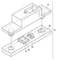
次に、テストパターン30を検出するためのトナー検出ユニット31の構成について説明する。図4及び図5はそれぞれ、トナー検出ユニット31の構成例を示す斜視図及び概略的な断面図である。トナー検出ユニット31は、図4に示すように、回路基板36に設けられた穴にハウジング37の突出部が挿入されることで、回路基板36に対してハウジング37が固定された構成を有している。図5は、回路基板36に対してハウジング37が固定された状態を示している。
<Configuration of Toner Detection Unit>
Next, the configuration of the
トナー検出ユニット31は、光学素子として、LED33(発光素子)及び2個の受光素子34,35を有している。LED33は、被照射体である中間転写ベルト12aに向けて光を照射する。即ち、LED33は、検出対象(測定対象物)であるトナーが付着した中間転写ベルト12aに向けて光を照射する。受光素子34,35は、LED33が中間転写ベルト12aに向けて照射した光の正反射光及び乱反射光をそれぞれ受光するために用いられる。トナー検出ユニット31において、ハウジング37は、LED33が中間転写ベルト12aに向けて照射した光の正反射光及び乱反射光をそれぞれ受光素子34,35に導くように構成されている。
The
LED33及び2個の受光素子34,35は、同一の回路基板36の表面(実装面)に直接実装され、回路基板36上で一列に実装されている。LED33が中間転写ベルト12aに向けて照射した光の正反射光及び乱反射光をそれぞれ受光する受光素子34,35は、回路基板36上で隣り合って配置されている。本実施形態では、受光素子34は、受光素子35よりもLED33から離れた位置に配置され、受光素子35は、受光素子34よりもLED33に近い位置に配置されている。また、図5に示すように、LED33と受光素子35との間には、LED33から出射された光が受光素子35によって直接受光されないようにするための遮光壁39が設けられている。
The
本実施形態の受光素子34,35は、LED33から出射される光の波長に対して感度を有するフォトトランジスタ(半導体)を一体化して基板にCOB実装した集積回路(IC)で構成されている。基板に実装されたフォトトランジスタは、透過性を有する樹脂材料で覆われている。受光素子34,35が実装された基板が回路基板36上に配置されている。本実施形態のLED33(発光素子)及び受光素子34,35は、赤外線を用いている。ただし、発光素子と受光素子の組み合わせに依存して受光素子が感度を有する波長の光であれば、その他の波長の光を使用する発光素子及び受光素子がトナー検出ユニット31に採用されてもよい。また、受光素子34,35として、フォトトランジスタに代えてフォトダイオードが用いられてもよい。
The
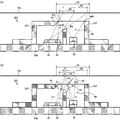
図5(a)に示すように、トナー検知ユニット31のハウジング37には、LED33から出射された光を中間転写ベルト12aに向けて導くための導光路60が設けられている。ハウジング37には、更に、LED33から出射された光の反射光を受光素子34,35にそれぞれ導くための導光路61,62が設けられている。導光路60,61は、ハウジング37に設けられた開口部によって構成されており、かつ、遮光壁38によって隔てられている。また、導光路62は、遮光壁38及び遮光壁39によって構成されており、遮光壁38によって導光路61と隔てられている。なお、導光路62は、ハウジング37の内部において、LED33から出射された光を被照射体である中間転写ベルト12aに向けて導く導光路60と一部が重なっており、これは、トナー検出ユニット31の小型化に貢献している。
As shown in FIG. 5A, the
遮光壁38は、後述する受光可能領域55からの乱反射光が受光素子35によって受光されないように(導光路62を通して受光素子35に入射しないように)するためのものである。遮光壁38は、ハウジング37に一体的に形成されており、回路基板36の実装面における受光素子35の位置の、当該実装面に対して垂直方向の上方(即ち、受光素子35の真上)に設けられ、ハウジング37の開口部付近まで形成されている。
The light-shielding
(LED33による光の照射領域54)
ここで、図5(a)に示す、LED33による光の照射領域54は、中間転写ベルト12aの外周面上(被照射体上)でLED33から光が照射される領域に相当する。照射領域54は、導光路60の左角60LとLED33の一方の端部とを結ぶ直線と、導光路60の右角60RとLED33の他方の端部とを結ぶ直線と、によって規定される。
(
Here, the
(受光素子34,35の受光可能領域55,56)
図5(a)に示す、受光素子34の受光可能領域55(第1領域)は、照射領域54のうちで、受光素子34が受光可能な光がLED33によって照射される領域(範囲)に相当し、照射領域54の一部の領域である。受光可能領域55は、導光路61の左角61Lと第1受光素子34の一方の端部を結ぶ直線と、導光路61の右角61Rと第1受光素子34の他方の端部とを結ぶ直線と、によって規定される。
図5(a)に示す、受光素子35の受光可能領域56(第2領域)は、照射領域54のうちで、受光素子35が受光可能な光がLED33によって照射される領域(範囲)に相当し、照射領域54の一部の領域である。受光可能領域56は、導光路62の左角62Lと受光素子35の一方の端部とを結ぶ直線と、導光路62の右角62Rと受光素子35の他方の端部とを結ぶ直線と、によって規定される。
(
The light-receiving area 55 (first area) of the light-receiving
The light-receiving area 56 (second area) of the light-receiving
本実施形態では、図5(a)に示すように、ハウジング37は、LED33の照射領域54のうちで、受光可能領域55からの正反射光を受光素子34に導き、受光可能領域56からの乱反射光を受光素子35に導くように構成されている。また、ハウジング37は、受光可能領域55と受光可能領域56とが互いに異なる領域となるように構成されている。なお、受光可能領域55と受光可能領域56とは、本実施形態では互いに重なり合わない領域となっているが、一部(例えば、各領域の端部)が重なっていてもよい。
In this embodiment, as shown in FIG. 5A, the
トナー検出ユニット31において、LED33から出射された光のうちで受光素子34が受光する正反射光は、図5(b)に示すように、導光路60内を光軸線50に沿った方向に進み、中間転写ベルト12aの外周面に照射される光である。中間転写ベルト12aの外周面からの正反射光は、概ね光軸線51に沿った方向に進み、ハウジング37の導光路61内に導かれて、受光素子34に到達して受光される。より具体的には、受光素子34は、LED33から照射される光のうち、受光可能領域55内の領域57に入射角θで入射し、反射角θで反射した光(正反射光)を受光するとともに、受光可能領域55に入射した光の乱反射光を受光することになる。
In the
一方、中間転写ベルト12aの外周面上の照射領域54に、トナー像であるテストパターン30が存在する場合、LED33から出射された光は、中間転写ベルト12aの外周面で正反射するとともにテストパターン30で乱反射する。このような反射光のうちの一部は、光軸線51に沿った方向に反射して受光素子34へ到達して受光され、他の一部は、光軸線53に沿った方向に反射して導光路62を通して受光素子35に到達して受光される。
On the other hand, when the
本実施形態では、図4及び図5に示すように、2個の受光素子34,35をICとして回路基板36上に実装することで、従来よりもトナー検出ユニット31の小型化を実現している。ここで、図6は、本実施形態に対する比較例(第1比較例)として示すトナー検出ユニット131の構成を示す断面図である。図6に示すトナー検出ユニット131では、LED33(発光素子)から出射された光の正反射光及び乱反射光をそれぞれ受光する2個の受光素子34,35は、独立した回路素子として回路基板136上に実装されている。また、このような実装に合わせて、ハウジング137には、LED33及び2個の受光素子34,35に対応する個別の開口部が設けられている。本実施形態のトナー検知ユニット31では、比較例として示すトナー検出ユニット131よりも、LED33及び2個の受光素子34,35が配列された方向(図6における水平方向)のサイズを小型化することが可能である。
In the present embodiment, as shown in FIGS. 4 and 5, by mounting the two
また、本実施形態のトナー検出ユニット31を用いると、中間転写ベルト12a上の2つの異なる領域(受光可能領域55,56)において同時にトナー像(テストパターン30)を検出することが可能である。例えば、2個の受光素子34,35が、中間転写ベルト12aの表面の移動方向と直交する方向に沿って配置されるように、トナー検出ユニット31を配置する。この場合、受光素子34,35の受光可能領域55,56も、中間転写ベルト12aの表面の移動方向と直交する方向に沿って配置される。その結果、トナー検出ユニット31を用いると、受光可能領域55及び受光可能領域56をそれぞれ通過するトナー像(テストパターン30)を、中間転写ベルト12aの回転位相が同位相となるタイミングに検出することができる。第2乃至第5実施形態では、トナー検出ユニット31のこのような特徴を利用したテストパターン30の検出及びその検出結果に基づく制御の例を示している。
Further, when the
なお、本実施形態のトナー検出ユニット31には、低濃度側と高濃度側とでトナーの検出精度が異なる受光素子を採用することも可能である。例えば、正反射光を受光する受光素子34は、低濃度側において高い検出精度を有する一方、乱反射光を受光する受光素子35は、高濃度側において高い検出精度を有していてもよい。このような場合にも、本実施形態のトナー検出ユニット31では、受光素子34による正反射光の受光結果と受光素子35による乱反射光の受光結果との両方を用いることによって、トナーの検出精度を高めることが可能である。
Note that the
<トナー検出ユニットの特性>
以下では、本実施形態のトナー検出ユニット31によるトナーの検出特性について説明する。まず、トナー検出特性についての説明に必要となる、受光素子34,35の受光光量及び光路長、中間転写ベルト12aの反射特性、並びに比較例について説明する。
<Characteristics of toner detection unit>
Hereinafter, the detection characteristics of the toner by the
(受光素子の受光光量及び光路長)
受光素子34,35が受光する光の強度(光量)である受光光量は、一般に、受光面積に比例し、かつ、光が通過する光路の長さ(光路長)の二乗に反比例する。このため、本実施形態では、受光素子34,35の受光光量は、それぞれの受光素子の受光可能領域55,56の面積に比例し、かつ、光路長の二乗に反比例することになる。
(Received light amount and optical path length of light receiving element)
The received light amount, which is the intensity (light amount) of light received by the
図5(b)に示すように、LED33から出射されて受光素子34が受光する光の光路長は、LED33の発光点の中心から受光可能領域55の中心までの距離LS1と、受光可能領域55の中心から受光素子34の受光面の中心までの距離LS2との和として表せる。一方、LED33から出射されて受光素子35が受光する光の光路長は、LED33の発光点の中心から受光可能領域56の中心までの距離LD1と、受光可能領域56の中心から受光素子35の受光面の中心までの距離LD2との和として表せる。即ち、
受光素子34が受光する光の光路長=LS1+LS2
受光素子35が受光する光の光路長=LD1+LD2
である。
As shown in FIG. 5B, the optical path length of the light emitted from the
Optical path length of light received by light receiving
Optical path length of light received by light receiving
It is.
(中間転写ベルトの反射特性)
図7は、中間転写ベルト12aの反射指向特性の一例を示す図である。図7(a)は、反射指向特性の測定結果を示し、図7(b)は、反射指向特性を測定方法の概念を示している。本測定では、図7(b)に示すように、中間転写ベルト12aの外周面に対する垂直方向を0°として、当該垂直方向から−15°回転した位置に点光源として配置したLED33(発光素子)から中間転写ベルト12aに光を照射する。更に、LED33から出射された光が照射される照射点(被照射面上の点)32から受光素子34までの距離を略等距離に維持しながら、受光素子34を−90°の位置から90°の位置まで回転移動させた場合の、受光素子34の出力値を測定する。
図7(a)は、このような測定によって得られた反射指向特性を示している。図7(a)に示すように、中間転写ベルト12aの反射特性は、正反射成分が支配的であるものの、正反射方向を中心とした角度幅72の乱反射成分も有している。即ち、中間転写ベルト12aは、正反射方向に高い強度の乱反射成分が存在する乱反射特性を有している。
(Reflection characteristics of the intermediate transfer belt)
FIG. 7 is a diagram illustrating an example of the reflection directivity characteristics of the
FIG. 7A shows the reflection directivity obtained by such a measurement. As shown in FIG. 7A, the reflection characteristic of the
(比較例)
図8及び図9はそれぞれ、本実施形態に対する比較例(第2比較例)として示すトナー検知ユニット231の構成を示す斜視図及び概略的な断面図である。図8及び図9に示すトナー検知ユニット231では、LED33(発光素子)及び2個の受光素子34,35は、同一の回路基板236の表面に直接実装され、回路基板236上で一列に配列されている。トナー検知ユニット231の受光素子34,35は、本実施形態のトナー検知ユニット31の受光素子34,35と同様、LED33が中間転写ベルト12aに向けて照射した光の正反射光及び乱反射光をそれぞれ受光するよう構成されている。
(Comparative example)
FIGS. 8 and 9 are a perspective view and a schematic cross-sectional view, respectively, showing the configuration of a
しかし、本比較例のトナー検知ユニット231の構成は、受光素子34,35の配置が図4及び図5に示す配置とは逆になっている点で、本実施形態のトナー検知ユニット31の構成と異なっている。即ち、トナー検知ユニット231では、受光素子34は、受光素子35よりもLED33に近い位置に配置され、受光素子35は、受光素子34よりもLED33から離れた位置に配置されている。なお、トナー検知ユニット231のハウジング237には、LED33から出射された光の正反射光及び乱反射光を受光素子34,35がそれぞれ受光できるように、LED33及び受光素子34,35の配置に依存した開口部が形成されている。
However, the configuration of the
(トナー検出特性)
次に、図8及び図9に示すトナー検出ユニット231のトナー検出特性を比較対象として、本実施形態のトナー検出ユニット31のトナー検出特性について説明する。図10は、濃度の異なるトナー像を順にテストパターン30として中間転写ベルト12a上に形成し、形成したテストパターン30をトナー検出ユニット31によって検出した場合の、受光素子34,35の出力の例を示す図である。図10(a)及び(b)は、本実施形態のトナー検出ユニット31の受光素子34,35の出力をそれぞれ示している。図10(c)及び(d)は、本実施形態のトナー検出ユニット31についての測定と同様の測定を行った場合に得られる、比較例のトナー検出ユニット231の受光素子34,35の出力をそれぞれ示している。
(Toner detection characteristics)
Next, the toner detection characteristics of the
ここで、トナー検出ユニット31は、対向する中間転写ベルト12aの表面の移動方向と直交する方向に沿って受光素子34,35が配置されるように、画像形成装置100内で位置付けられている。この場合、受光素子34,35の受光可能領域55,56も、中間転写ベルト12aの表面の移動方向と直交する方向に沿って配置される。受光素子34,35は、受光可能領域55,56からの反射光を受光して、受光光量に対応する値の検出信号を生成及び出力する。なお、中間転写ベルト12aの表面の移動方向及び当該移動方向と直交する方向は、それぞれ、レーザビームによる感光ドラム1の走査における副走査方向及び主走査方向と対応している。図10では、主走査方向において照射領域54と同じまたはそれより広い範囲にテストパターン30を形成して得られる、受光素子34,35の出力の測定結果を示している。即ち、テストパターン30が受光可能領域55,56を通過する際に、同じテストパターンが受光素子34,35によって検出されるようにしている。
Here, the
図10は、トナーの濃度が0%から100%まで20%ずつ段階的に上昇するテストパターン30を中間転写ベルト12a上に形成し、トナー検出ユニット31によって検出した場合の、受光素子34,35の出力の変化を示している。図10の各グラフには、受光素子34,35の受光可能領域55,56を通過する(即ち、検出対象となる)トナーの濃度[%]を記載している。濃度0%に対応する出力値101,102は、受光可能領域55,56にトナー像が形成されておらず、中間転写ベルト12aの表面(外周面)からの反射光を受光素子34,35がそれぞれ受光した場合の出力値に相当する。
FIG. 10 shows the
まず、図10(a)は、本実施形態のトナー検出ユニット31における、LED33から出射された光の正反射光を受光する受光素子34の出力を示している。受光素子34の出力値は、テストパターン30が形成されていない中間転写ベルト12aの表面からの反射光を受光した場合に最大値(出力値101)となっている。これは、図7を用いて説明したように、中間転写ベルト12aは、光学特性として乱反射特性を若干有しているものの、正反射特性の方が支配的であるためである。また、受光素子34の出力値は、テストパターン30(トナー像)からの反射光を受光した場合、トナーの濃度が増加するほど低くなっている。これは、トナーの乱反射特性に起因して、トナーの濃度が増加するほどトナーからの正反射光の光量が少なくなるためである。
First, FIG. 10A shows the output of the
図10(a)に示す受光素子34の出力は、図10(c)に示す比較例の受光素子34の出力と比べると、同様の傾向を示しているものの、比較例よりも全体的に値がわずかに小さいことがわかる。このような出力値の差は、受光素子34が受光する光の光路長(LS1+LS2)に依存している。具体的には、図5(b)に示すトナー検出ユニット31の構成と図9(b)に示す比較例の構成とを比べると、本実施形態の構成では、比較例の構成よりもLED33と受光素子34との距離が長く、入射角(反射角)θが大きい。このため、本実施形態の構成では、比較例の構成よりも光路長(LS1+LS2)が長く、その結果として受光素子34の出力に差が生じている。
The output of the
しかし、図10(a)及び図10(c)に示すように、そのような受光素子34の出力の差はわずかである。これは、受光素子34が受光する正反射光は比較的高い指向性を有し、光路長の差によって生じる正反射光の受光光量の差が少ないためである。本実施形態のトナー検出ユニット31は、上述のように、比較例のトナー検出ユニット231と比べて受光素子34の出力がわずかに小さくなる特性を有しているものの、十分なトナー検出性能を有している。具体的には、図10(a)に示すように、中間転写ベルト12aの表面からの反射光を受光素子34が受光した場合の出力値101(最大値)と、各濃度のトナー像からの反射光を受光素子34が受光した場合の出力値との間には、十分な差分が存在する。このため、本実施形態のトナー検出ユニット31を用いた場合、受光素子34の出力値と閾値との比較処理により、中間転写ベルト12a上の(受光可能領域55における)トナーの有無及びトナーの濃度を十分な精度で判定することができる。
However, as shown in FIGS. 10A and 10C, the difference between the outputs of the
次に、図10(b)は、本実施形態のトナー検出ユニット31における、LED33から出射された光の乱反射光を受光する受光素子35の出力を示している。受光素子35の出力は、トナーの濃度の変化に対して受光素子34の出力(図10(a))とは逆の傾向の変化を示している。具体的には、受光素子35の出力値は、テストパターン30が形成されていない中間転写ベルト12aの表面からの反射光を受光した場合に最小値(出力値102)となっている。これは、中間転写ベルト12aの乱反射特性が弱いためである。また、受光素子35の出力値は、テストパターン30(トナー像)からの反射光を受光した場合、トナーの濃度が増加するほど高くなっている。これは、トナーの乱反射特性に起因して、トナーの濃度が増加するほどトナーからの乱反射光の光量が多くなるためである。
Next, FIG. 10B shows the output of the
図10(b)示す受光素子35の出力は、図10(d)に示す比較例の受光素子35の出力と比べると、比較例よりも最大値は大きい一方で最小値(出力値102)は小さく、即ち、比較例よりも最小値と最大値との差分103が大きいことがわかる。また、本実施形態では、中間転写ベルト12aの表面からの反射光を受光素子35が受光した場合の出力値102(最小値)と、各濃度のトナー像からの反射光を受光素子35が受光した場合の出力値との間には、比較例と比べて大きな差分が存在する。このため、本実施形態のトナー検出ユニット31を用いた場合、受光素子35の出力値と閾値との比較処理により、中間転写ベルト12a上の(受光可能領域56における)トナーの有無及びトナーの濃度を、比較例よりも高い精度で判定することができる。
The output of the
次に、本実施形態のトナー検出ユニット31と比較例のトナー検出ユニット231とで、LED33から出射された光の乱反射光を受光する受光素子35の出力に差が生じる(即ち、トナー検出性能に差が生じる)理由について説明する。
Next, the
まず、LED33の照射領域54(受光可能領域56)にテストパターン30が形成されていない場合の、図10(b)に示す出力値102と図10(d)に示す出力値102との差について説明する。図9(b)に示す比較例の構成では、受光素子35は、概ね光軸線51に沿った正反射方向に進む乱反射光と、光軸線53に沿った方向に進む乱反射光との両方を受光するように構成されている。光軸線53に沿って進む乱反射光は、光路長が比較的長く(LD1+LD2)、低い強度で受光素子35によって受光される。一方で、正反射方向に進む乱反射光は、光路長が比較的短い(LS1+LS2)ことだけでなく、中間転写ベルト12aの上述の乱反射特性に起因して、比較的高い強度で受光素子35によって受光される。このため、図10(d)に示すように、比較例のトナー検出ユニット231における受光素子35の出力値102は、中間転写ベルト12aの表面からの反射光の受光光量に相当する分だけ増えている。これは、受光素子35の出力における、トナーの検出に有効な振幅成分が小さくなることを意味する。
First, the difference between the
これに対し、図5(b)に示す本実施形態の構成では、受光素子35は、光軸線53に沿った方向に進む乱反射光を受光し、概ね光軸線51に沿った正反射方向に進む乱反射光を受光しないように構成されている。具体的には、LED33から光軸線50に沿って進み、中間転写ベルト12aの表面で光軸線51に沿った方向に反射した光の乱反射成分は、遮光壁38によって遮られ、受光素子35へ入射することはない。また、LED33から光軸線52に沿って進んだ光の反射光の、比較的高い強度の乱反射成分は、中間転写ベルト12aから光軸線53'の方向に進むことになり、この乱反射成分が受光素子35に入射することはない。このため、図10(b)に示すように、本実施形態のトナー検出ユニット31では、中間転写ベルト12aの表面からの反射光を受光素子35が受光した場合の出力値102が、比較例(図10(d))よりも抑えられている。これは、受光素子35の出力における、トナーの検出に有効な振幅成分が大きくなることを意味する。
On the other hand, in the configuration of the present embodiment illustrated in FIG. 5B, the
次に、LED33の照射領域54(受光可能領域56)にテストパターン30が形成されている場合の、図10(b)に示す出力値と図10(d)に示す出力値との差について説明する。ここで、濃度100%のトナー像(ベタ画像)からの反射光を受光した場合の受光素子35の出力値に着目すると、図10(b)に示す出力値は、図10(d)に示す出力値(比較例)よりも大きくなっている。これは、比較例のトナー検出ユニット231は、LED33と受光素子35との距離が相対的に長い構成を有しているのに対して、本実施形態のトナー検出ユニット31は、LED33と受光素子35との距離が相対的に短い構成を有しているためである。即ち、本実施形態のトナー検出ユニット31は、受光素子35が受光する光の光路長(LD1+LD2)が、比較例のトナー検出ユニット231よりも短いため、より高い強度で乱反射光を受光できる。
Next, the difference between the output value shown in FIG. 10B and the output value shown in FIG. 10D when the
このように、本実施形態のトナー検出ユニット31では、受光素子34の受光可能領域55と受光素子35の受光可能領域56とが互いに重なり合わない領域となるように、回路基板36に取り付けられるハウジング37が構成される。これにより、受光素子35が、トナー像からの乱反射光を受光する場合の受光光量を相対的に多くする一方で、中間転写ベルト12aの表面からの乱反射光を受光する場合の受光光量を相対的に少なくすることを可能にしている。本実施形態のトナー検出ユニット31では、更に、LED33(発光素子)が出射した光の乱反射光を受光する受光素子35が、LED33が出射した光の正反射光を受光する受光素子34よりもLED33に近い位置に配置される。これにより、受光素子35が、トナー像からの乱反射光を受光する場合の受光光量を、相対的に更に多くすることを可能にしている。なお、トナー検出ユニット31は、受光可能領域55,56の両方に対して、共通のLED33(発光素子)が光を十分に照射できるように(即ち、受光可能領域55,56の両方が照射領域54に含まれるように)構成される。
As described above, in the
本実施形態のトナー検出ユニット31の構成によれば、中間転写ベルト12aの表面からの反射光を受光した場合の受光素子35の出力値102は、比較例のトナー検出ユニット231の出力値よりも小さくなる。また、最大濃度(100%)のトナー像からの反射光を受光した場合の受光素子35の出力値は、比較例のトナー検出ユニット231の出力値よりも大きくなる。即ち、本実施形態のトナー検出ユニット31の構成によれば、各濃度のトナー像からの反射光を受光した場合の受光素子35の出力値と、出力値102(最小値)との差分(例えば差分103)を、より大きくすることが可能である。
According to the configuration of the
したがって、本実施形態のトナー検出ユニット31では、LED33から出射した光の乱反射光の、受光素子35による受光結果に基づいて、受光可能領域56におけるトナーの有無及びトナーの濃度を、比較例よりも高い精度で判定することが可能である。即ち、LED33から出射した光の乱反射光の受光結果に基づくトナー検出(トナーの有無及び濃度の判定)の性能に関して、本実施形態のトナー検出ユニット31は、比較例のトナー検出ユニット231よりも優れた性能を有している。
Therefore, in the
<トナー検出ユニット31の他の特徴>
本実施形態のトナー検出ユニット31は、図5に示すように、正反射光を受光する受光素子34の受光可能領域55よりも、乱反射光を受光する受光素子35の受光可能領域56の方が広くなるように構成されている。図10を用いて上述したように、LED33から出射された光の正反射光は、比較的高い指向性を有する強い光である。これに対して、LED33から出射された光の乱反射光は、様々な方向に拡散しており、低い指向性を有する弱い光である。このため、本実施形態では、受光素子35による乱反射光の受光光量が多くなるよう、正反射光を受光するための受光可能領域55よりも乱反射光を受光するための受光可能領域56を広くしている。即ち、図5に示すように、受光可能領域56は、受光可能領域55よりも、受光素子34と受光素子35とが配列された方向におけるサイズが大きくなっている。
<Other Features of
As shown in FIG. 5, in the
また、本実施形態のトナー検出ユニット31では、LED33(発光素子)から出射された光は、ハウジング37に設けられた導光路60を通ってハウジング37から出射される。LED33から出射された光の乱反射光は、導光路62を通して受光素子35に入射する。トナー検出ユニット31は、LED33から出射される光の、ハウジング37からの出口と、受光素子35が受光する乱反射光の、ハウジング37への入口とが共通となるよう、構成されている。即ち、ハウジング37には、LED33から出射された光と、受光素子34,35にそれぞれ入射する光とを絞るための共通の開口部が形成されている。これにより、LED33から出射される光の出口と乱反射光の入口とが異なる場合と比較して、LED33と受光素子35との間の距離を短くすることが可能である。その結果、受光素子35が受光する光の光路長(LD1+LD2)をより短くするとともに、受光素子34が受光する光の光路長(LS1+LS2)もより短くすることが可能である。したがって、受光素子34,35のそれぞれが受光する光の光量をより増加させ、受光結果を示す各受光素子からの出力値をより大きな値にすることが可能である。
In the
なお、本実施形態では、2個の受光素子34,35は、トナー検出ユニット31の小型化のために一体化されているが、独立した回路素子として、本実施形態と同様の位置に近接して配置されてもよい。その場合にも、本実施形態と同様の効果を得ることが可能なトナー検出ユニット31を実現できる。
In the present embodiment, the two
以上説明したように、本実施形態のトナー検出ユニット31は、中間転写ベルト12aに向けて光を照射するLED33と、LED33から出射された光の正反射光及び乱反射光をそれぞれ受光するための受光素子34,35とを備える。これらのLED33及び受光素子34,35は、回路基板36上に一列に実装されている。回路基板36には、LED33から出射された光を中間転写ベルト12aに向けて導く導光路と、正反射光及び乱反射光をそれぞれ受光素子34,35に導く導光路とが設けられている。具体的には、ハウジング37は、LED33の照射領域54のうちで、受光可能領域55からの正反射光を受光素子34に導き、受光可能領域55と異なる受光可能領域56からの乱反射光を受光素子35に導くように構成される。本実施形態によれば、トナー検出ユニット31の、LED33及び受光素子34,35の配列方向のサイズの小型化を実現しつつ、乱反射光の受光結果に基づくトナー検出の性能に関して、(比較例のトナー検出ユニット231よりも)優れた性能を実現できる。
As described above, the
[第2実施形態]
第2乃至第5実施形態では、第1実施形態で説明したトナー検知ユニット31の使用例として、トナー検出ユニット31による検出に有利なテストパターンを用いて色ずれ補正制御を行う例について説明する。
[Second embodiment]
In the second to fifth embodiments, as an example of use of the
一般に、色ずれには、静的な要因による色ずれ(静的な色ずれ)と、動的な要因による、色ずれ量が周期的に変動する色ずれ(動的な色ずれ)がある。静的な要因は、画像の書き出し位置の誤差等である。動的な要因は、搬送ベルト等の駆動ローラの駆動むらや感光ドラムの回転むら等に起因する、搬送ベルト(記録材搬送ベルトや中間転写ベルト等)の速度変動である。中間転写ベルトに形成したテストパターンを光学センサで検出して(静的な)色ずれ量を測定する場合、その測定結果には、テストパターンの検出タイミングに依存した大きさの動的な色ずれ成分によって、誤差が生じる。(例えば、特開2002−14507号公報を参照。)このような動的な色ずれ成分は、色ずれ量測定用の基準色及び対象色のパッチ画像を検出するタイミング(動的な色ずれ成分についての変動の位相)がずれるほど大きくなる。 Generally, color misregistration includes color misregistration due to static factors (static color misregistration) and color misregistration due to dynamic factors (dynamic color misregistration) in which the color misregistration amount fluctuates periodically. Static factors include errors in the image writing start position. The dynamic factor is a speed fluctuation of a transport belt (a recording material transport belt, an intermediate transfer belt, or the like) due to drive unevenness of a drive roller such as a transport belt or rotation unevenness of a photosensitive drum. When the (static) color misregistration amount is measured by detecting the test pattern formed on the intermediate transfer belt with an optical sensor, the measurement result includes a dynamic color misregistration having a size dependent on the test pattern detection timing. The components cause errors. (For example, refer to Japanese Patent Application Laid-Open No. 2002-14507.) Such a dynamic color misregistration component is a timing (dynamic color misregistration component) for detecting a patch image of a reference color and a target color for measuring a color misregistration amount. The phase of the fluctuation of
上述の測定誤差を低減するには、例えば特開2002−14507号公報に記載のように、搬送ベルトの移動方向に沿って、動的な色ずれ成分の複数の位相に対応する複数のパターンを形成して、動的な色ずれ成分をキャンセルできるようにする必要がある。しかし、搬送ベルトの移動方向(副走査方向)に沿って複数のパターンを形成すると、当該複数のパターンの、副走査方向の全長が長くなり、色ずれ補正制御(キャリブレーション)に要する時間も長くなる問題がある。 In order to reduce the above measurement error, for example, as described in JP-A-2002-14507, a plurality of patterns corresponding to a plurality of phases of a dynamic color misregistration component are formed along the moving direction of the transport belt. It must be formed so that dynamic color shift components can be canceled. However, when a plurality of patterns are formed along the moving direction (sub-scanning direction) of the transport belt, the total length of the plurality of patterns in the sub-scanning direction increases, and the time required for color misregistration correction control (calibration) also increases. There is a problem.
これに対し、図4及び図5に示すトナー検出ユニット31を用いる場合、上述のように、中間転写ベルト12a上の2つの異なる領域(受光可能領域55,56)において同時にトナー像を検出することが可能である。そこで、本実施形態では、このようなトナー検出ユニット31の特性を利用して、副走査方向における同じ位置に(即ち、略同位相の)基準色及び対象色のパッチ画像を配置したテストパターンを形成する。これにより、それらのパッチ画像を受光素子34,35で同時に検出できるようにする。このように、動的な色ずれ成分についての変動の位相が同位相となるタイミングに基準色及び対象色のパッチ画像を検出できる場合、動的な色ずれ成分の影響を受けずに(静的な)色ずれ量を測定できる。この場合、動的な色ずれ成分をキャンセルするための、上述のような複数の位相に対応した複数のテストパターンを形成する必要がない点で有利である。以下では、第1実施形態との相違点を中心として本実施形態について説明する。
On the other hand, when the
<テストパターンの例>
本実施形態では、トナー検出ユニット31(光学センサ)の光源波長における中間転写ベルト12aの反射率が、正反射光についてはいずれの色のトナー像よりも高く、乱反射光についてはいずれの色のトナー像よりも低い場合について説明する。この場合、中間転写ベルト12aからの正反射光及び乱反射光のいずれもトナー検出ユニット31によって良好に検出できる。
<Example of test pattern>
In the present embodiment, the reflectance of the
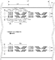
図11は、感光ドラム1の1回転周期に対応する距離Ld1におけるテストパターン30の一例を示す図である。図11において、中間転写ベルト12a上の領域155は、当該領域にトナー像が形成された場合、中間転写ベルト12aによる搬送中に当該トナー像が受光素子34の受光可能領域55を通過する領域に相当する。また、中間転写ベルト12a上の領域156は、当該領域にトナー像が形成された場合、中間転写ベルト12aによる搬送中に当該トナー像が受光素子35の受光可能領域56を通過する領域に相当する。以下では、領域155を「正反射受光領域」、領域156を「乱反射受光領域」と称する。
FIG. 11 is a diagram illustrating an example of the
図11に示すように、正反射受光領域155及び乱反射受光領域156には、それぞれ独立したテストパターン(トナー像)が並列に形成される。また、中間転写ベルト12aの表面の移動方向(トナー画像の搬送方向)に沿って、副走査方向の色ずれ量の検出用のテストパターン30vと主走査方向の色ずれ量の検出用のテストパターン30mとが交互に配置されている。テストパターン30v,30mは、それぞれ、複数のトナー像(トナーパッチ)である複数のパッチ画像を含むパッチ画像群で構成されている。このように、本実施形態のテストパターン30は、テストパターン30v及びテストパターン30mを含む。なお、中間転写ベルト12aの表面の移動方向及び当該移動方向と直交する方向は、それぞれ、レーザビームによる感光ドラム1の走査における副走査方向及び主走査方向と対応している。
As shown in FIG. 11, independent test patterns (toner images) are formed in parallel in the regular reflection
テストパターン30vは、中間転写ベルト12a上の正反射受光領域155に副走査方向に沿って配置される、色ずれ量検出の基準となる基準色のパッチ画像Pstd1a,Pstd2a,Pstd3a,Pstd4aを含む。テストパターン30vは、更に、中間転写ベルト12a上の乱反射受光領域156に副走査方向に沿って配置される、基準色を基準とした色ずれ量検出の対象となる対象色のパッチ画像Ptgt1a,Ptgt2a,Ptgt3a,Ptgt4aを含む。対象色のパッチ画像Ptgt1a,Ptgt2a,Ptgt3a,Ptgt4aは、それぞれ、基準色のパッチ画像Pstd1a,Pstd2a,Pstd3a,Pstd4aと、副走査方向において略同位相となるように配置される。なお、対象色のパッチ画像Ptgt1a,Ptgt2a,Ptgt3a,Ptgt4aは、それぞれ異なる色のトナーを用いて形成される。
The
テストパターン30mは、中間転写ベルト12a上の正反射受光領域155に副走査方向に沿って配置される、基準色のパッチ画像Pstd1b,Pstd2b,Pstd3b,Pstd4bと、基準色のパッチPstd1c,Pstd2c,Pstd3c,Pstd4cと、を含む。テストパターン30mは、更に、中間転写ベルト12a上の乱反射受光領域156に副走査方向に沿って配置される、対象色のパッチ画像Ptgt1b,Ptgt2b,Ptgt3b,Ptgt4bと、対象色のパッチ画像Ptgt1c,Ptgt2c,Ptgt3c,Ptgt4cと、を含む。対象色のパッチ画像Ptgt1b,Ptgt2b,Ptgt3b,Ptgt4bは、それぞれ、基準色のパッチ画像Pstd1b,Pstd2b,Pstd3b,Pstd4bと、副走査方向において略同位相となるように配置される。また、対象色のパッチ画像Ptgt1c,Ptgt2c,Ptgt3c,Ptgt4cは、それぞれ、基準色のパッチ画像Pstd1c,Pstd2c,Pstd3c,Pstd4cと、副走査方向において略同位相となるように配置される。なお、対象色のパッチ画像Ptgt1b,Ptgt2b,Ptgt3b,Ptgt4bは、それぞれ異なる色のトナーを用いて形成され、対象色のパッチ画像Ptgt1c,Ptgt2c,Ptgt3c,Ptgt4cは、それぞれ異なる色のトナーを用いて形成される。
The
図11の例では、テストパターン30vを、副走査方向において、感光ドラム1の半回転周期に対応する逆位相の距離Ld2の間隔で繰り返し形成している。これにより、パターンを繰り返すことによって、感光ドラム1の回転むらに起因する、色ずれ量の検出誤差成分をキャンセルできるようになる。なお、中間転写ベルト12a上でテストパターンの形成が可能な領域に依存して、感光ドラム1の1/3回転周期や1/4回転周期等に対応するテストパターンを更に形成してもよい。これにより、感光ドラム1の回転むらに起因する、色ずれ量の検出誤差成分をより高い精度でキャンセルできるようになる。
In the example of FIG. 11, the
<副走査方向の色ずれ量検出>
次に図12(a)を参照して、基準色に対する対象色の副走査方向の色ずれ量を、図11に示すテストパターン30vを用いて検出(測定)する方法について説明する。ここでは、基準色をブラック(K)、対象色をイエロー(Y)とした場合の、基準色に対する対象色の色ずれ量の検出を例に説明する。
<Detection of color shift amount in sub-scanning direction>
Next, a method of detecting (measuring) the color shift amount of the target color in the sub-scanning direction with respect to the reference color using the
図12(a)は、図11に示すテストパターン30vの一部として、基準色であるKのパッチ画像Pstd1aと、対象色であるYのパッチ画像Ptgt1aとを拡大して示している。上述のように、基準色(K)のパッチ画像Pstd1a及び対象色(Y)のパッチ画像Ptgt1aは、それぞれ、受光可能領域55,56のサイズに合わせたサイズを有している。第1実施形態で説明したように、受光可能領域55よりも受光可能領域56の方が広いため、対象色(Y)のパッチ画像Ptgt1aは、基準色(K)のパッチ画像Pstd1aよりも主走査方向及び副走査方向のサイズが大きくなっている。
FIG. 12A shows, as a part of the
正反射受光領域155に形成されたパッチ画像Pstd1aは、中間転写ベルト12aの表面の移動に伴って搬送される間に、トナー検出ユニット31に含まれる受光素子34の受光可能領域55を通過する。制御ユニット41(CPU)は、受光素子34による、中間転写ベルト12a及びパッチ画像Pstd1aからの正反射光の受光結果に基づいて、パッチ画像Pstd1aの副走査方向における先端及び後端を検出する。制御ユニット41は、パッチ画像Pstd1aの先端の検出タイミングTstd1apと後端の検出タイミングTstd1asとを、それぞれパッチ画像の先端及び後端の位置として検出する。
The patch image Pstd1a formed in the regular reflection
一方、乱反射受光領域156に形成されたパッチ画像Ptgt1aは、中間転写ベルト12aの表面の移動に伴って搬送される間に、トナー検出ユニット31に含まれる受光素子35の受光可能領域56を通過する。制御ユニット41は、受光素子35による、中間転写ベルト12a及びパッチ画像Ptgt1aからの乱反射光の受光結果に基づいて、パッチ画像Ptgt1aの副走査方向における先端及び後端を検出する。制御ユニット41は、パッチ画像Ptgt1aの先端の検出タイミングTtgt1apと後端の検出タイミングTtgt1asとを、それぞれパッチ画像の先端及び後端の位置として検出する。
On the other hand, the patch image Ptgt1a formed in the irregular reflection
制御ユニット41は、このようにして得られたデータから、基準色(K)のパッチ画像Pstd1aの先端Tstd1apと後端Tstd1asとの間の中心位置Tstd1aと、対象色(Y)のパッチ画像Ptgt1aの先端Ttgt1apと後端Ttgt1asとの間の中心位置Ttgt1aとを算出する。更に、制御ユニット41は、基準色(K)のパッチ画像Pstd1aの中心位置Tstd1aと対象色(Y)のパッチ画像Ptgt1aの中心位置Ttgt1aとの差Dtgt1a(=Ttgt1a−Tstd1a)を、基準色(K)に対する対象色(Y)の、副走査方向の色ずれ量として算出する。制御ユニット41は、このような色ずれ量の算出結果を用いることで、上述の色ずれ補正制御(例えば、書き出しタイミングの調整等による副走査方向の色ずれ補正)を行うことが可能である。
The
<主走査方向の色ずれ量検出>
次に図12(b)を参照して、基準色に対する対象色の主走査方向の色ずれ量を、図11に示すテストパターン30mを用いて検出(測定)する方法について説明する。ここでは、図12(a)と同様、基準色をブラック(K)、対象色をイエロー(Y)とした場合の、基準色に対する対象色の色ずれ量の検出を例に説明する。
<Detection of color shift amount in main scanning direction>
Next, a method of detecting (measuring) the color shift amount of the target color in the main scanning direction with respect to the reference color using the
図12(b)は、図11で示すテストパターン30mの一部として、基準色であるKのパッチ画像Pstd1bと、対象色であるYのパッチ画像Ptgt1bとを拡大して示している。図12(b)に示すように、各パッチ画像は、主走査方向の色ずれ量の検出を可能にするために、中間転写ベルト12aの表面の移動方向(副走査方向)に対して傾斜角度45°を有している。また、上述のように、パッチ画像Pstd1bとパッチ画像Ptgt1bとは、副走査方向において略同位相となるように配置されている。
FIG. 12B shows, as a part of the
正反射受光領域155に形成されたパッチ画像Pstd1bは、中間転写ベルト12aの表面の移動に伴って搬送される間に、受光素子34の受光可能領域55を通過する。制御ユニット41は、受光素子34による正反射光の受光結果に基づいて、パッチ画像Pstd1bの副走査方向における先端及び後端を検出する。制御ユニット41は、パッチ画像Pstd1bの先端の検出タイミングTstd1bpと後端の検出タイミングTstd1bsとを、それぞれパッチ画像の先端及び後端の位置として検出する。
The patch image Pstd1b formed in the regular reflection
一方、乱反射受光領域156に形成されたパッチ画像Ptgt1bは、中間転写ベルト12aの表面の移動に伴って搬送される間に、受光素子35の受光可能領域56を通過する。制御ユニット41は、受光素子35による乱反射光の受光結果に基づいて、パッチ画像Ptgt1bの副走査方向における先端及び後端を検出する。制御ユニット41は、パッチ画像Ptgt1bの先端の検出タイミングTtgt1bpと後端の検出タイミングTtgt1bsとを、それぞれパッチ画像の先端及び後端の位置として検出する。
On the other hand, the patch image Ptgt1b formed in the irregular reflection
制御ユニット41は、このようにして得られたデータから、基準色(K)のパッチ画像Pstd1bの先端Tstd1bpと後端Tstd1bsとの間の中心位置Tstd1bと、対象色(Y)のパッチ画像Ptgt1bの先端Ttgt1bpと後端Ttgt1bsとの間の中心位置Ttgt1bとを算出する。更に、制御ユニット41は、基準色(K)のパッチ画像Pstd1bの中心位置Tstd1bと対象色(Y)のパッチ画像Ptgt1bの中心位置Ttgt1bとの差Dtgt1b(=Ttgt1b−Tstd1b)を算出する。ここで、テストパターン30mに含まれる各パッチ画像の傾斜角度が45°である。このため、副走査方向の色ずれが存在しない条件下では、算出されたDtgt1bを、基準色(K)に対する対象色(Y)の、主走査方向の色ずれ量として扱うことが可能である。制御ユニット41は、このような色ずれ量の算出結果を用いることで、上述の色ずれ補正制御(例えば、書き出しタイミングの調整等による主走査方向の色ずれ補正)を行うことが可能である。
The
以上説明したように、本実施形態では、トナー検出ユニット31の受光可能領域55,56が重複しないことを利用して、基準色及び対象色のパッチ画像を副走査方向において略同位相で配置したテストパターン30を中間転写ベルト12a上に形成する。更に、受光素子34,35を用いてテストパターン30を検出することで、色ずれ量を検出(測定)する。
As described above, in the present embodiment, the patch images of the reference color and the target color are arranged in substantially the same phase in the sub-scanning direction by utilizing the fact that the light-receiving
このように、第1実施形態で説明したトナー検出ユニット31を用いることで、副走査方向において略同位相に形成した基準色及び対象色のパッチ画像を使用して色ずれ量の検出が可能である。これにより、中間転写ベルト12aの動的な色ずれ成分(感光ドラム間の距離のずれに伴う動的な色ずれ成分は除く。)を除去しながら色ずれ量の検出を行うことが可能である。即ち、中間転写ベルト12aの、例えば1/4回転周期等に対応する打ち消し処理が不要となるため、動的な色ずれ成分をキャンセルするための、動的な色ずれ成分の複数の位相に対応した複数のテストパターンを形成する必要がなくなる。このため、テストパターンの単位長さ当たりの色ずれ量の検出精度を向上させることが可能となり、副走査方向におけるテストパターン30の全長を短くすることが可能である。これにより、テストパターン30を形成するためのトナー消費量を削減でき、また、色ずれ量の検出に要する時間及び色ずれ補正制御に要する時間を短くすることが可能である。
As described above, by using the
なお、本実施形態では、基準色をブラック(K)、対象色をイエロー(Y)として、副走査方向及び主走査方向の色ずれ量の検出について説明したが、他の色の組み合わせについても同様に色ずれ量の検出が可能である。また、本実施形態で用いたテストパターン30v,30m(図11)は一例にすぎず、パターン形状、パターンの間隔、色の組合せ等の特性が異なるテストパターンが用いられてもよい。更に、副走査方向における対象色のパッチ画像の並び順は、図11に示す順と異なっていてもよい。本実施形態では、受光素子34側の正反射受光領域155に基準色のパッチ画像を、受光素子35側の乱反射受光領域156に対象色のパッチ画像を形成する例を示している。しかし、受光素子35側に乱反射受光領域156に基準色のパッチ画像、受光素子34側の正反射受光領域155に対象色のパッチ画像を形成してもよい。
In the present embodiment, the detection of the color misregistration amount in the sub-scanning direction and the main scanning direction is described with the reference color being black (K) and the target color being yellow (Y), but the same applies to other color combinations. It is possible to detect the amount of color misregistration. The
[第3実施形態]
第3実施形態では、上述の実施形態で説明したトナー検出ユニット31において同一の回路基板36上に実装された受光素子34,35の、副走査方向及び主走査方向の相対的な位置ずれを補正する例について説明する。以下では、第1及び第2実施形態との相違点を中心として本実施形態について説明する。
[Third embodiment]
In the third embodiment, in the
第2実施形態では、基準色と対象色とを異なる色とすることで、基準色と対象色との間の色ずれ量を検出している。これに対して、基準色と対象色とを同一色として第2実施形態における色ずれ量の検出と同様の処理を行うと、トナー検出ユニット31上(回路基板36上)における、受光素子34,35の相対的な位置ずれ量を検出することが可能である。本実施形態では、一例として、基準色及び対象色を同一色のブラック(K)として、受光素子34の位置を基準とした受光素子35の相対的な位置ずれ量を検出している。
In the second embodiment, the color difference between the reference color and the target color is detected by setting the reference color and the target color to be different colors. On the other hand, when the same processing as the detection of the amount of color misregistration in the second embodiment is performed by setting the reference color and the target color to be the same color, the
<副走査方向の位置ずれ量検出>
図13(a)は、図11に示すテストパターン30vの一部として、基準色のパッチ画像Pstd4aと、基準色と同一色の対象色のパッチ画像Ptgt4aとを拡大して示している。第2実施形態で説明したように、基準色のパッチ画像Pstd4aは正反射受光領域155に、対象色のパッチ画像Ptgt4aは乱反射受光領域156に、それぞれ形成される。
<Detection of displacement in sub-scanning direction>
FIG. 13A shows, as a part of the
制御ユニット41は、受光素子34による正反射光の受光結果に基づいて、正反射受光領域155に形成されている基準色のパッチ画像Pstd4aの副走査方向における先端Tstd4ap及び後端Tstd4asを検出する。また、制御ユニット41は、受光素子35による乱反射光の受光結果に基づいて、乱反射受光領域156に形成されている対象色のパッチ画像Ptgt4aの副走査方向における先端Ttgt4ap及び後端Ttgt4asを検出する。制御ユニット41は、このようにして得られたデータから、基準色(K)のパッチ画像Pstd4aの中心位置Tstd4aと、対象色(K)のパッチ画像Ptgt4aの中心位置Ttgt4aとを算出する。更に、制御ユニット41は、それらの中心位置の差Dsns4a(Dsns4a=Ttgt4a−Tstd4a)を、受光素子34と受光素子35との間の副走査方向の位置ずれ量として算出する。
The
制御ユニット41は、算出した位置ずれ量Dsns4aを、第2実施形態における色ずれ量の検出値Dtgt1aに対する補正値として用いて、色ずれ補正制御を行う。即ち、制御ユニット41は、色ずれ量の検出値Dtgt1aを位置ずれ量Dsns4aによって補正した値(=Dtgt1a+Dsns4a)を用いて、上述の色ずれ補正制御(例えば、書き出しタイミングの調整等による副走査方向の色ずれ補正)を行う。これにより、色ずれ補正制御における補正精度を向上させることが可能である。
The
<主走査方向の位置ずれ量検出>
図13(b)は、図11に示すテストパターン30mの一部として、基準色のパッチ画像Pstd4bと、基準色と同一色の対象色のパッチ画像Ptgt4bとを拡大して示している。第2実施形態で説明したように、基準色のパッチ画像Pstd4bは正反射受光領域155に、対象色のパッチ画像Ptgt4bは乱反射受光領域156に、それぞれ形成される。第2実施形態と同様、各パッチ画像は、受光素子34,35の主走査方向の位置ずれ量の検出を可能にするために、中間転写ベルト12aの表面の移動方向(副走査方向)に対して傾斜角度45°を有している。
<Detection of displacement in main scanning direction>
FIG. 13B shows a patch image Pstd4b of a reference color and a patch image Ptgt4b of a target color identical to the reference color as a part of the
制御ユニット41は、受光素子34による正反射光の受光結果に基づいて、正反射受光領域155に形成されている基準色のパッチ画像Pstd4bの副走査方向における先端Tstd4bpと後端Tstd4bsを検出する。また、制御ユニット41は、受光素子35による乱反射光の受光結果に基づいて、乱反射受光領域156に形成されている対象色のパッチ画像Ptgt4bの副走査方向における先端Ttgt4bp及び後端Ttgt4bsを検出する。制御ユニット41は、このようにして得られたデータから、基準色(K)のパッチ画像Pstd4bの中心位置Tstd4bと、対象色(K)のパッチ画像Ptgt4bの中心位置Ttgt4bとを算出する。更に、制御ユニット41は、それらの中心位置の差Dsns4b(Dsns4b=Ttgt4b−Tstd4b)を、受光素子34と受光素子35との間の主走査方向の位置ずれ量として算出する。
The
制御ユニット41は、算出した位置ずれ量Dsns4bを、第2実施形態における色ずれ量の検出値Dtgt1bに対する補正値として用いて、色ずれ補正制御を行う。即ち、制御ユニット41は、色ずれ量の検出値Dtgt1bを位置ずれ量Dsns4bによって補正した値(=Dtgt1b+Dsns4b)を用いて、上述の色ずれ補正制御(例えば、書き出しタイミングの調整等による主走査方向の色ずれ補正)を行う。これにより、色ずれ補正制御における補正精度を向上させることが可能である。
The
以上説明したように、本実施形態では、基準色と対象色とを同一色として第2実施形態における色ずれ量の検出と同様の処理を行うことで、同一の回路基板36上に実装された受光素子34と受光素子35との間の相対的な位置ずれ量を検出できる。更に、検出した位置ずれ量を第2実施形態における色ずれ補正制御に適用することで、色ずれ補正の精度を向上させることが可能である。なお、本実施形態では、基準色及び対象色をブラック(K)として、受光素子34,35の位置ずれ量の検出について説明したが、他の色を用いても同様に位置ずれ量の検出が可能である。
As described above, in the present embodiment, the reference color and the target color are set to the same color, and the same processing as the detection of the color misregistration amount in the second embodiment is performed. The relative displacement between the light receiving
[第4実施形態]
第4実施形態では、トナー検出ユニット31(光学センサ)の光源波長における中間転写ベルト12aの反射率が、第2及び第3実施形態における反射率と異なる場合の、色ずれ量の検出について説明する。具体的には、中間転写ベルト12aの反射率が、正反射光については、いずれの色のトナー像よりも高く、乱反射光については、ブラック(K)以外の色(Y,M,C)のトナー像よりも低く、Kのトナー像とは略同等である場合について説明する。この場合、ブラック(K)以外の色(Y,M,C)のトナー像については、トナー検出ユニット31によって、正反射光及び乱反射光のいずれを用いても精度良く検出可能である。しかし、Kのトナー像については、中間転写ベルト12a上でトナー像が形成されている領域からの乱反射光と、トナー像が形成されていない領域からの乱反射光とで、受光素子35による受光光量が同等の光量となり、トナー像の検出が難しくなる。
[Fourth embodiment]
In the fourth embodiment, detection of the amount of color misregistration when the reflectance of the
そこで、本実施形態では、中間転写ベルト12a上の乱反射受光領域156にブラック(K)のトナー像を形成する場合は、K以外の色の、反射率が異なる(高い)トナー像を、Kのトナー像の下地画像として形成することを特徴としている。即ち、K以外の反射率の高い色のトナー像に対して、Kのトナー像を重ねて形成することで、Kのトナー像の境界の検出精度を高めることを可能にする。なお、以下では、第1乃至第3実施形態との相違点を中心として本実施形態について説明する。
Therefore, in the present embodiment, when a black (K) toner image is formed in the irregular reflection
本実施形態では、基準色をマゼンタ(M)、対象色をブラック(K)とした場合の、基準色に対する対象色の、副走査方向の色ずれ量の検出を例に説明する。図14は、図11に示すテストパターン30vの一部として、基準色(M)のパッチ画像Pstd2aと、対象色(K)のパッチ画像Ptgt2aとを拡大して示している。基準色のパッチ画像Pstd2aは正反射受光領域155に、対象色のパッチ画像Ptgt2aは乱反射受光領域156に、それぞれ形成される。本実施形態では、乱反射受光領域156に、対象色(K)のパッチ画像Ptgt2aの下地画像として、対象色のパッチ画像よりもサイズが大きいイエロー(Y)のパッチ画像Ppri2aが形成されている。即ち、Yのパッチ画像Ppri2aの上にKのパッチ画像Ptgt2aが重ねて形成されている。
In the present embodiment, detection of the amount of color shift in the sub-scanning direction of the target color with respect to the reference color when the reference color is magenta (M) and the target color is black (K) will be described as an example. FIG. 14 shows a patch image Pstd2a of the reference color (M) and a patch image Ptgt2a of the target color (K) in an enlarged manner as a part of the
制御ユニット41は、第2及び第3実施形態と同様、受光素子34による正反射光の受光結果に基づいて、正反射受光領域155に形成されている基準色(M)のパッチ画像Pstd2aの副走査方向における先端Tstd2ap及び後端Tstd2asを検出する。また、制御ユニット41は、受光素子35による乱反射光の受光結果に基づいて、乱反射受光領域156に形成されている対象色のパッチ画像Ptgt2aの副走査方向における先端Ttgt2ap及び後端Ttgt2asを検出する。その際、制御ユニット41は、対象色のパッチ画像Ptgt2aと、下地画像として形成されたYのパッチ画像Ppri2aとの境界から、パッチ画像Ptgt2aの先端及び後端として検出する。
As in the second and third embodiments, the
制御ユニット41は、このようにして得られたデータから、基準色(M)のパッチ画像Pstd2aの中心位置Tstd2aと、対象色(K)のパッチ画像Ptgt2aの中心位置Ttgt2aとを算出する。更に、制御ユニット41は、基準色(M)のパッチ画像Pstd2aの中心位置Tstd2aと対象色(K)のパッチ画像Ptgt2aの中心位置Ttgt2aとの差Dtgt2a(=Ttgt2a−Tstd2a)を、基準色(M)に対する対象色(K)の、副走査方向の色ずれ量として算出する。制御ユニット41は、このような色ずれ量の算出結果を用いることで、第2及び第3実施形態と同様に、色ずれ補正制御(例えば、書き出しタイミングの調整等による副走査方向の色ずれ補正)を行うことが可能である。
The
以上説明したように、本実施形態では、乱反射光について、下地画像と対象色のパッチ画像との間の反射率の差が、中間転写ベルト12aの表面と対象色のパッチ画像との間の反射率の差よりも大きくなるように、下地画像を形成している。本実施形態によれば、ブラック(K)等の、反射光に占める乱反射成分の割合が少ない色のパッチ画像を、テストパターン30として乱反射受光領域156に形成した場合にも、色ずれ量の検出精度が劣化することを防止できる。
As described above, in the present embodiment, for diffusely reflected light, the difference in reflectance between the base image and the target color patch image is caused by the reflection between the surface of the
なお、本実施形態では、基準色をマゼンタ(M)、対象色をブラック(K)、下地画像として形成するパッチ画像の色をイエロー(Y)として、副走査方向の色ずれ量の検出について説明したが、他の色の組み合わせについても同様に色ずれ量の検出が可能である。主走査方向の色ずれ量の検出についても、図14に示すテストパターン30vと同様に下地画像となるパッチ画像を形成することで、第2実施形態と同様の処理により実現することが可能である。また、本実施形態における中間転写ベルト12aの反射率は一例にすぎない。例えば、中間転写ベルト12a上の正反射受光領域155または乱反射受光領域156に、中間転写ベルト12aの反射率と略同等の反射率のトナー像を形成する場合には、反射率が高いトナー像を下地画像とすることで、本実施形態と同様の効果を期待できる。
In the present embodiment, detection of the amount of color misregistration in the sub-scanning direction will be described with the reference color being magenta (M), the target color being black (K), and the color of the patch image to be formed as the base image being yellow (Y). However, the color shift amount can be similarly detected for other color combinations. The detection of the color misregistration amount in the main scanning direction can be realized by the same processing as that of the second embodiment by forming a patch image serving as a base image similarly to the
[第5実施形態]
第5実施形態では、第4実施形態の変形例について説明する。一般に、トナー検出ユニット31の受光素子34,35として用いられるような光学素子は、受光光量が少ないほど応答速度が低下する特性を有している。本実施形態では、このような受光光量に依存した光学素子の応答速度の差を考慮して、トナー検出ユニット31を用いてより精度良く色ずれ量の検出及び色ずれ補正制御を実現する方法について説明する。なお、以下では、第1乃至第4実施形態との相違点を中心として本実施形態について説明する。
[Fifth Embodiment]
In the fifth embodiment, a modified example of the fourth embodiment will be described. Generally, an optical element used as the
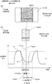
図15は、図14と同様、正反射受光領域155には、基準色(M)のパッチ画像Pstd4aを形成し、乱反射受光領域156には、Yのパッチ画像Ppri4aを下地として形成して、対象色(K)のパッチ画像Ptgt4aを重ねて形成した状態を示している。図15は、更に、正反射受光領域155及び乱反射受光領域156に形成されたパッチ画像を受光素子34,35を用いて検出した場合の、受光素子34,35の出力の変化を示している。
In FIG. 15, similarly to FIG. 14, a patch image Pstd4a of the reference color (M) is formed in the regular reflection
図15において、波形Mは受光素子34の出力波形、波形Nは受光素子35の出力波形である。出力波形M,Nは、図15に示すように、受光素子34,35の受光光量に応じて鈍った形状の波形となる。制御ユニット41は、受光素子34,35から出力されるこのような形状の出力波形M,Nに基づいて、出力波形M,Nが閾値電圧Aと交差する2点の間の中心位置を、パッチ画像の副走査方向における中心位置として算出する。このため、正反射受光領域155に形成されたパッチ画像Pstd4aの副走査方向における中心位置Tstd4aと、受光素子34の出力波形Mに基づいて算出される中心位置Tstd4a'との間には、誤差ΔTstd4aが生じる。また、同様に、乱反射受光領域156に形成されたパッチ画像Ptgt4aの副走査方向における中心位置Ttgt4aと、受光素子35の出力波形Nに基づいて算出される中心位置Ttgt4a'との間には、誤差ΔTtgt4aが生じる。
In FIG. 15, a waveform M is an output waveform of the
図15に示すような、受光素子34,35の出力波形の鈍りの程度は、受光素子34,35の受光光量が少ないほど大きくなり、その結果として上述の誤差が大きくなる。特に、受光素子35が受光する乱反射光は、様々な方向に拡散しており、低い指向性を有する弱い光である。このため、受光素子35による乱反射光の受光結果には、受光素子34による正反射光の受光結果よりも大きな誤差が生じる傾向がある。
As shown in FIG. 15, the degree of bluntness of the output waveforms of the
本実施形態では、上述の誤差が低減されるように、各色の副走査方向の色ずれ量を検出する。具体的には、画像形成装置100におけるキャリブレーションとは別に、各色について図15に示すような受光素子34,35の出力波形を事前に取得して、上述の誤差を算出しておく。更に、算出した誤差を、画像形成装置100が備える不揮発性メモリ(図示せず)等の記憶デバイスに補正値として予め格納しておく。即ち、受光素子34,35の受光光量に応じた応答速度の変化によって色ずれ量の検出値に生じる誤差を補正するための補正値を、記憶デバイスに格納しておく。制御ユニット41は、第2乃至第4実施形態で説明した方法で取得した色ずれ量を、当該補正値を使用して補正(オフセット)する。これにより、受光素子34,35の応答速度に起因して生じる色ずれ量の検出誤差を低減することが可能である。
In the present embodiment, the amount of color misregistration of each color in the sub-scanning direction is detected so that the above-described error is reduced. Specifically, separately from the calibration in the
なお、本実施形態では、副走査方向の色ずれ量の検出について説明したが、主走査方向の色ずれ量の検出に対しても、同様に実現できる。また、本実施形態では、基準色をマゼンタ(M)、対象色をブラック(K)、下地として形成するパッチ画像の色をイエロー(Y)として、副走査方向の色ずれ量の検出について説明したが、他の色の組み合わせについても同様に色ずれ量の検出が可能である。 In the present embodiment, the detection of the color shift amount in the sub-scanning direction has been described. However, the detection of the color shift amount in the main scanning direction can be similarly realized. In the present embodiment, detection of the amount of color misregistration in the sub-scanning direction has been described, with the reference color being magenta (M), the target color being black (K), and the color of the patch image to be formed as the base being yellow (Y). However, the color misregistration amount can be similarly detected for other color combinations.
100:画像形成装置、1:感光ドラム、31:トナー検出ユニット、12a:中間転写ベルト、30:テストパターン、33:LED、34,35:受光素子、36:回路基板、37:ハウジング、38,39:遮光壁、41:制御ユニット 100: image forming apparatus, 1: photosensitive drum, 31: toner detection unit, 12a: intermediate transfer belt, 30: test pattern, 33: LED, 34, 35: light receiving element, 36: circuit board, 37: housing, 38, 39: light shielding wall, 41: control unit
Claims (27)
前記照射光が前記被照射体の照射領域で乱反射された乱反射光を受光するための第1受光素子と、
前記照射光が前記被照射体の前記照射領域で正反射された正反射光を受光するための第2受光素子と、を備え、
前記第1受光素子は、前記照射領域のうち、第1領域で乱反射した前記乱反射光を受光し、前記第2受光素子は、主走査方向において少なくとも一部は前記第1領域を含まない第2領域で正反射した前記正反射光を受光する
ことを特徴とする光学センサ。 A light-emitting element that irradiates irradiation light toward an irradiation target;
A first light receiving element for receiving irregularly reflected light in which the irradiation light is irregularly reflected in an irradiation area of the irradiation target;
A second light-receiving element for receiving the regular reflection light in which the irradiation light is regularly reflected in the irradiation region of the irradiation object,
The first light receiving element receives the irregularly reflected light that is irregularly reflected in a first area of the irradiation area, and the second light receiving element includes a second light receiving element that at least partially does not include the first area in a main scanning direction. An optical sensor, which receives the specularly reflected light regularly reflected in a region.
を更に備えることを特徴とする請求項1に記載の光学センサ。 A first opening that is an opening for determining an irradiation area of the irradiation light with respect to the irradiation target, the first opening through which the irradiation light passes, and through which the irregularly reflected light received by the first light receiving element passes. 2. The optical sensor according to claim 1, further comprising: a housing forming an opening and a second opening through which the specularly reflected light received by the second light receiving element passes. 3.
ことを特徴とする請求項2に記載の光学センサ。 The housing forms a third opening in a region between the first opening and the first light receiving element, through which the irregularly reflected light passing through the first opening passes before being received by the first light receiving element. The optical sensor according to claim 2, wherein:
ことを特徴とする請求項2又は3に記載の光学センサ。 The optical sensor according to claim 2, wherein the housing covers the light emitting element, the first light receiving element, and the second light receiving element.
ことを特徴とする請求項2から4のいずれか1項に記載の光学センサ。 In a region until the irradiation light passes through the first opening, a part of a first optical path through which the irradiation light passes and a second optical path through which the irregularly reflected light received by the first light receiving element passes The optical sensor according to any one of claims 2 to 4, wherein?
ことを特徴とする請求項1から5のいずれか1項に記載の光学センサ。 The optical sensor according to any one of claims 1 to 5, wherein a distance between the first light receiving element and the light emitting element is shorter than a distance between the second light receiving element and the light emitting element.
ことを特徴とする請求項1から6のいずれか1項に記載の光学センサ。 The optical sensor according to any one of claims 1 to 6, wherein the first light receiving element and the second light receiving element are arranged adjacently on a circuit board.
ことを特徴とする請求項2から5のいずれか1項に記載の光学センサ。 The optical device according to any one of claims 2 to 5, wherein the housing has a first light blocking wall for blocking light other than the irregularly reflected light from being received by the first light receiving element. Sensor.
ことを特徴とする請求項8に記載の光学センサ。 The first light-shielding wall is provided above a position of the first light-receiving element on a mounting surface of a circuit board on which the first light-receiving element and the second light-receiving element are mounted, in a direction perpendicular to the mounting surface. The optical sensor according to claim 8, wherein:
ことを特徴とする請求項2から5、8及び9のいずれか1項に記載の光学センサ。 The housing is provided between the light emitting element and the first light receiving element, and is for blocking light emitted from the light emitting element so as not to be directly received by the first light receiving element and the second light receiving element. The optical sensor according to claim 2, further comprising a second light-shielding wall.
ことを特徴とする請求項1に記載の光学センサ。 The direction in which the first light receiving element and the second light receiving element are arranged is such that the first area has a larger area irradiated with the irradiation light than the second area. The optical sensor according to any of the preceding claims.
ことを特徴とする請求項1に記載の光学センサ。 The optical sensor according to claim 1, wherein the first region and the second region are regions that are part of the irradiation region and do not overlap with each other.
ことを特徴とする請求項1から12のいずれか1項に記載の光学センサ。 The optical sensor according to any one of claims 1 to 12, wherein the first light receiving element and the second light receiving element are mounted on a circuit board as one integrated circuit.
ことを特徴とする請求項2に記載の光学センサ。 The optical sensor according to claim 2, wherein the first opening is an opening for regulating the irradiation light and regulating the irregularly reflected light and the regular reflected light.
ことを特徴とする請求項2に記載の光学センサ。 The second opening is configured such that, in a region between the first opening and the first light receiving element and the second light receiving element, the irregularly reflected light received by the first light receiving element passes therethrough, and the second light receiving element The optical sensor according to claim 2, wherein the optical sensor is an opening through which the specularly reflected light received by the optical sensor passes.
ことを特徴とする請求項2又は15に記載の光学センサ。 A first optical path through which the irradiation light passes, a second optical path through which the irregularly reflected light received by the first light receiving element passes, and a second light path through which the irradiation light passes through the first opening. The optical sensor according to claim 2 or 15, wherein a part of each of the third optical path through which the regular reflection light received by the two light receiving elements passes overlaps.
前記照射光が前記被照射体の照射領域で乱反射された乱反射光を受光するための第1受光素子と、
前記照射光が前記被照射体の前記照射領域で正反射された正反射光を受光するための第2受光素子と、
前記発光素子から出射された光を前記被照射体に向けて導くための第1開口と、前記照射領域のうち、第1領域で乱反射した前記乱反射光を前記第1受光素子に導くための第2開口と、主走査方向において少なくとも一部は前記第1領域を含まない第2領域で正反射した前記正反射光を前記第2受光素子に導く第3開口と、を形成するハウジングと、
を備えることを特徴とする光学センサ。 A light-emitting element that irradiates irradiation light toward an irradiation target;
A first light receiving element for receiving irregularly reflected light in which the irradiation light is irregularly reflected in an irradiation area of the irradiation target;
A second light receiving element for receiving the regular reflection light in which the irradiation light is regularly reflected in the irradiation region of the irradiation target;
A first opening for guiding the light emitted from the light emitting element toward the irradiation target; and a first opening for guiding the irregularly reflected light diffusely reflected in the first region to the first light receiving element in the irradiation region. A housing that forms two openings, and a third opening that guides the specularly reflected light that is at least partially reflected in the second region not including the first region in the main scanning direction to the second light receiving element;
An optical sensor comprising:
請求項1から17のいずれか1項に記載の光学センサであって、前記像担持体の表面と対向する位置に設けられ、前記発光素子から前記被照射体である前記像担持体に向けて光を照射する、前記光学センサと、
前記像担持体に形成された画像が、前記照射光が照射される前記像担持体の照射領域内の第1領域または第2領域を通過する際の、前記第1受光素子または前記第2受光素子から出力される信号に基づいて、前記画像の位置または濃度を検出する制御手段であって、検出した前記画像の位置に基づいて色ずれ補正制御を実行する、または検出した前記画像の濃度に基づいて画像濃度制御を実行する制御手段と、
を備えることを特徴とする画像形成装置。 An image carrier;
The optical sensor according to any one of claims 1 to 17 , wherein the optical sensor is provided at a position facing a surface of the image carrier, and is directed from the light emitting element to the image carrier, which is the object to be irradiated. Irradiating light, the optical sensor,
The first light receiving element or the second light receiving element when an image formed on the image carrier passes through a first area or a second area in an irradiation area of the image carrier irradiated with the irradiation light; Control means for detecting the position or density of the image based on a signal output from the element, wherein the color shift correction control is executed based on the detected position of the image, or the density of the detected image is Control means for performing image density control based on
An image forming apparatus comprising:
請求項1から17のいずれか1項に記載の光学センサであって、前記像担持体の表面と対向する位置に、前記像担持体の表面の移動方向と直交する方向に沿って第1領域及び第2領域が配置されるように設けられ、前記発光素子から前記被照射体である前記像担持体に向けて光を照射する、前記光学センサと、
前記像担持体の表面において、前記第1領域を通過する第1パッチ画像と、前記第2領域を通過する前記第1パッチ画像とは異なる色の第2パッチ画像と、を前記移動方向において同じ位置になるように形成する画像形成手段と、
前記第1パッチ画像が前記第1領域を通過する際に前記第1受光素子から出力される信号と、前記第2パッチ画像が前記第2領域を通過する際に前記第2受光素子から出力される信号とに基づいて、色ずれ量を検出する制御手段であって、検出した前記色ずれ量に基づいて、色ずれ補正制御を行う制御手段と、
を備えることを特徴とする画像形成装置。 An image carrier;
The optical sensor according to any one of claims 1 to 17 , wherein a first region is provided at a position facing the surface of the image carrier along a direction orthogonal to a moving direction of the surface of the image carrier. And an optical sensor that is provided so that the second region is arranged, and irradiates light from the light emitting element toward the image carrier that is the object to be irradiated,
On the surface of the image carrier, a first patch image passing through the first area and a second patch image different in color from the first patch image passing through the second area are the same in the moving direction. Image forming means for forming the image so as to be positioned
A signal output from the first light receiving element when the first patch image passes through the first area, and a signal output from the second light receiving element when the second patch image passes through the second area. Control means for detecting a color misregistration amount based on the detected color misregistration amount, based on the detected color misregistration amount,
An image forming apparatus comprising:
ことを特徴とする請求項19に記載の画像形成装置。 20. The image forming apparatus according to claim 19 , wherein a length of the first patch image in a direction orthogonal to the moving direction is longer than a length of the second patch image in a direction orthogonal to the moving direction.
ことを特徴とする請求項19に記載の画像形成装置。 The control unit detects a position of the first patch image based on a signal output from the first light receiving element when the first patch image passes through the first region, and detects the position of the second patch image. Detecting the position of the second patch image based on a signal output from the second light receiving element when the light passes through the second region, thereby detecting the color shift amount. Item 20. The image forming apparatus according to Item 19 .
前記制御手段は、更に、前記第3パッチ画像及び前記第4パッチ画像がそれぞれ前記第1領域及び前記第2領域を通過する際に前記第1受光素子及び前記第2受光素子からそれぞれ出力される信号に基づいて、前記第3パッチ画像の位置と前記第4パッチ画像の位置との差分を、前記第1受光素子と前記第2受光素子との間の位置ずれ量として検出する ことを特徴とする請求項19から21のいずれか1項に記載の画像形成装置。 The image forming means further includes, on the surface of the image carrier, a third patch image passing through the first area, and a fourth patch image having the same color as the third patch image passing through the second area. , Are formed at the same position in the moving direction,
The control unit is further output from the first light receiving element and the second light receiving element when the third patch image and the fourth patch image pass through the first area and the second area, respectively. Detecting a difference between the position of the third patch image and the position of the fourth patch image as a positional shift amount between the first light receiving element and the second light receiving element based on the signal. The image forming apparatus according to any one of claims 19 to 21 .
ことを備えることを特徴とする請求項22に記載の画像形成装置。 23. The image forming apparatus according to claim 22 , wherein the control unit performs the color shift correction control based on the detected color shift amount and the detected position shift amount.
ことを特徴とする請求項19から23のいずれか1項に記載の画像形成装置。 When forming the first patch image, the image forming unit may use, as a base of the first patch image, a base image having a size larger than that of the first patch image and a reflectance different from that of the first patch image. the image forming apparatus according to any one of claims 19, characterized in that the formation 23.
ことを特徴とする請求項24に記載の画像形成装置。 For the irregularly reflected light, a difference in reflectance between the base image and the first patch image is larger than a difference in reflectance between the surface of the image carrier and the first patch image. The image forming apparatus according to claim 24 , wherein
前記制御手段は、前記記憶手段に格納されている補正値で前記色ずれ量の検出値を補正する
ことを特徴とする請求項19から25のいずれか1項に記載の画像形成装置。 A storage unit storing a correction value for correcting an error generated in the detection value of the color shift amount due to a change in a response speed according to a light receiving amount of the first light receiving element and the second light receiving element,
It said control means, the image forming apparatus according to any one of claims 19 to 25, characterized in that to correct the detection value of the color shift amount by the correction value stored in the storage means.
前記光学センサからの信号に基づいて画像形成条件を制御する制御手段と、
を備えることを特徴とする画像形成装置。 The optical sensor according to any one of claims 1 to 17 , wherein the optical sensor irradiates light from the light emitting element toward the irradiation target on which an image is formed, and
Control means for controlling image forming conditions based on a signal from the optical sensor,
An image forming apparatus comprising:
Priority Applications (1)
| Application Number | Priority Date | Filing Date | Title |
|---|---|---|---|
| JP2017044224A JP6675344B2 (en) | 2017-03-08 | 2017-03-08 | Optical sensor and image forming apparatus |
Applications Claiming Priority (1)
| Application Number | Priority Date | Filing Date | Title |
|---|---|---|---|
| JP2017044224A JP6675344B2 (en) | 2017-03-08 | 2017-03-08 | Optical sensor and image forming apparatus |
Related Parent Applications (1)
| Application Number | Title | Priority Date | Filing Date |
|---|---|---|---|
| JP2015218797A Division JP6140247B2 (en) | 2015-11-06 | 2015-11-06 | Optical sensor and image forming apparatus |
Related Child Applications (1)
| Application Number | Title | Priority Date | Filing Date |
|---|---|---|---|
| JP2020037155A Division JP6849889B2 (en) | 2020-03-04 | 2020-03-04 | Optical sensor and image forming device |
Publications (3)
| Publication Number | Publication Date |
|---|---|
| JP2017103497A JP2017103497A (en) | 2017-06-08 |
| JP2017103497A5 JP2017103497A5 (en) | 2018-12-13 |
| JP6675344B2 true JP6675344B2 (en) | 2020-04-01 |
Family
ID=59015694
Family Applications (1)
| Application Number | Title | Priority Date | Filing Date |
|---|---|---|---|
| JP2017044224A Active JP6675344B2 (en) | 2017-03-08 | 2017-03-08 | Optical sensor and image forming apparatus |
Country Status (1)
| Country | Link |
|---|---|
| JP (1) | JP6675344B2 (en) |
Families Citing this family (2)
| Publication number | Priority date | Publication date | Assignee | Title |
|---|---|---|---|---|
| JP2019207364A (en) | 2018-05-30 | 2019-12-05 | 株式会社リコー | Image forming apparatus, image forming method, and program |
| JP2021092433A (en) * | 2019-12-10 | 2021-06-17 | コニカミノルタ株式会社 | Image formation apparatus and glossiness measuring method |
Family Cites Families (5)
| Publication number | Priority date | Publication date | Assignee | Title |
|---|---|---|---|---|
| JP5463959B2 (en) * | 2010-03-03 | 2014-04-09 | 株式会社リコー | Reflective optical sensor and image forming apparatus |
| JP6061703B2 (en) * | 2012-02-13 | 2017-01-18 | キヤノン株式会社 | Optical sensor and image forming apparatus |
| JP6004812B2 (en) * | 2012-07-30 | 2016-10-12 | キヤノン株式会社 | Optical detection apparatus and image forming apparatus |
| JP6355066B2 (en) * | 2013-08-29 | 2018-07-11 | 株式会社リコー | Sensor device and image forming apparatus |
| JP5761390B2 (en) * | 2014-01-22 | 2015-08-12 | 株式会社リコー | Reflective optical sensor and image forming apparatus |
-
2017
- 2017-03-08 JP JP2017044224A patent/JP6675344B2/en active Active
Also Published As
| Publication number | Publication date |
|---|---|
| JP2017103497A (en) | 2017-06-08 |
Similar Documents
| Publication | Publication Date | Title |
|---|---|---|
| JP6140247B2 (en) | Optical sensor and image forming apparatus | |
| JP6630309B2 (en) | Optical sensor and image forming apparatus | |
| US8369725B2 (en) | Image forming apparatus and method of correcting image concentration | |
| JP6793449B2 (en) | Image forming device | |
| KR20130126529A (en) | Image forming apparatus for performing registration and density correction control | |
| US8811845B2 (en) | Registration mark and image forming apparatus | |
| JP6675344B2 (en) | Optical sensor and image forming apparatus | |
| JP4841389B2 (en) | Image forming apparatus | |
| JP2007225709A (en) | Image forming apparatus | |
| JP2009042375A (en) | Image forming device | |
| JP2009139575A (en) | Light amount detector, misalignment amount detector, and image density detector | |
| JP6849889B2 (en) | Optical sensor and image forming device | |
| JP5370856B2 (en) | Image forming apparatus | |
| JP5636780B2 (en) | Image forming apparatus | |
| US8150302B2 (en) | Image forming apparatus and image forming method that detects an amount of color misalignment using reflected light | |
| JP5114256B2 (en) | Image forming apparatus and image forming method | |
| US9977365B2 (en) | Image forming apparatus with correction of exposure light using measurement image | |
| JP2020013039A (en) | Image forming apparatus | |
| JP2019197111A (en) | Image forming apparatus | |
| JP7370774B2 (en) | Image forming device | |
| JP2014048338A (en) | Image forming device and image forming method | |
| JP2020016791A (en) | Image formation device | |
| JP2017090511A (en) | Optical detector and image forming apparatus | |
| JP2019086285A (en) | Image forming apparatus, color shift correcting method | |
| JP2004101793A (en) | Color image forming apparatus |
Legal Events
| Date | Code | Title | Description |
|---|---|---|---|
| A521 | Request for written amendment filed |
Free format text: JAPANESE INTERMEDIATE CODE: A523 Effective date: 20181030 |
|
| A621 | Written request for application examination |
Free format text: JAPANESE INTERMEDIATE CODE: A621 Effective date: 20181030 |
|
| A131 | Notification of reasons for refusal |
Free format text: JAPANESE INTERMEDIATE CODE: A131 Effective date: 20191129 |
|
| A521 | Request for written amendment filed |
Free format text: JAPANESE INTERMEDIATE CODE: A523 Effective date: 20200116 |
|
| TRDD | Decision of grant or rejection written | ||
| A01 | Written decision to grant a patent or to grant a registration (utility model) |
Free format text: JAPANESE INTERMEDIATE CODE: A01 Effective date: 20200210 |
|
| A61 | First payment of annual fees (during grant procedure) |
Free format text: JAPANESE INTERMEDIATE CODE: A61 Effective date: 20200310 |
|
| R151 | Written notification of patent or utility model registration |
Ref document number: 6675344 Country of ref document: JP Free format text: JAPANESE INTERMEDIATE CODE: R151 |