US9257652B2 - Photoelectric conversion material, method for producing the same, and organic photovoltaic cell containing the same - Google Patents
Photoelectric conversion material, method for producing the same, and organic photovoltaic cell containing the same Download PDFInfo
- Publication number
- US9257652B2 US9257652B2 US13/778,440 US201313778440A US9257652B2 US 9257652 B2 US9257652 B2 US 9257652B2 US 201313778440 A US201313778440 A US 201313778440A US 9257652 B2 US9257652 B2 US 9257652B2
- Authority
- US
- United States
- Prior art keywords
- polymer
- photoelectric conversion
- electron
- conversion material
- organic photovoltaic
- Prior art date
- Legal status (The legal status is an assumption and is not a legal conclusion. Google has not performed a legal analysis and makes no representation as to the accuracy of the status listed.)
- Expired - Fee Related, expires
Links
- 238000006243 chemical reaction Methods 0.000 title claims abstract description 88
- 239000000463 material Substances 0.000 title claims abstract description 46
- 238000013086 organic photovoltaic Methods 0.000 title claims description 31
- 238000004519 manufacturing process Methods 0.000 title claims description 11
- 229920000642 polymer Polymers 0.000 claims abstract description 87
- 229910021389 graphene Inorganic materials 0.000 claims abstract description 12
- -1 polyphenylene Polymers 0.000 claims description 30
- 229920000265 Polyparaphenylene Polymers 0.000 claims description 24
- 238000006116 polymerization reaction Methods 0.000 claims description 22
- 238000000034 method Methods 0.000 claims description 15
- 239000000203 mixture Substances 0.000 claims description 6
- 239000007795 chemical reaction product Substances 0.000 claims description 5
- 125000000843 phenylene group Chemical group C1(=C(C=CC=C1)*)* 0.000 claims description 3
- 230000000379 polymerizing effect Effects 0.000 claims description 3
- 238000004768 lowest unoccupied molecular orbital Methods 0.000 description 26
- 229920000301 poly(3-hexylthiophene-2,5-diyl) polymer Polymers 0.000 description 24
- MCEWYIDBDVPMES-UHFFFAOYSA-N [60]pcbm Chemical compound C123C(C4=C5C6=C7C8=C9C%10=C%11C%12=C%13C%14=C%15C%16=C%17C%18=C(C=%19C=%20C%18=C%18C%16=C%13C%13=C%11C9=C9C7=C(C=%20C9=C%13%18)C(C7=%19)=C96)C6=C%11C%17=C%15C%13=C%15C%14=C%12C%12=C%10C%10=C85)=C9C7=C6C2=C%11C%13=C2C%15=C%12C%10=C4C23C1(CCCC(=O)OC)C1=CC=CC=C1 MCEWYIDBDVPMES-UHFFFAOYSA-N 0.000 description 20
- 238000004770 highest occupied molecular orbital Methods 0.000 description 17
- 238000002835 absorbance Methods 0.000 description 8
- 125000003118 aryl group Chemical group 0.000 description 8
- 230000005525 hole transport Effects 0.000 description 7
- SIHLBXHNCFPHDW-UHFFFAOYSA-N CC.CC.CC.CC.CC1=CC2=C(C=C1)C1=C/C3=C4C5=C\1C1=C2/C=C\C2=C1\C1=C/5C5=C6/C7=C(C=CC=C7C7=C8C9=C(C=C7)C7=CC=CC=C7C7=C\9C(=C2\C=C/7)/C1=C/86)C1=C/5C\4=C(\C=C/1)C1=CC=CC=C13.CC1=CC2=C(C=C1)C1=C3C4=C(/C=C\C=C=42)/C2=C\C=C4C5=C6C7=C8\C9=C(C=CC%10=C9/C6=C(/C=C\5)C5=CC=CC=C5%10)C5=C6C(=CC=C5)C5=C9C(=CC=C5)C(=C/1)/C1=C3\C2=C\4C\7=C1/C9=C\68.CC1=CC=C2C(=C1)C1=C3C(=CC=C1)C1=C4\C5=C3C2=CC2=C5/C3=C5\C6=C(/C=C\C=C\26)C2=C6\C5=C5/C7=C(C=CC8=C7/C6=C(/C=C\2)C2=CC=CC=C28)C2=CC=CC6=C2C5=C3\C4=C6\C=C\1.CC1=CC=C2C(=C1)C1=C3C4=C(\C=C/1)C1=CC=CC5=C1\C1=C/4C4=C6\C7=C8\C(=C/C=C7/C7=C9/C%10=C(\C=C/7)C7=CC=CC=C7C7=C%10C(=C5C=C7)/C1=C\96)\C1=C(C=CC=C1)C1=C/C2=C/3C/4=C\18 Chemical compound CC.CC.CC.CC.CC1=CC2=C(C=C1)C1=C/C3=C4C5=C\1C1=C2/C=C\C2=C1\C1=C/5C5=C6/C7=C(C=CC=C7C7=C8C9=C(C=C7)C7=CC=CC=C7C7=C\9C(=C2\C=C/7)/C1=C/86)C1=C/5C\4=C(\C=C/1)C1=CC=CC=C13.CC1=CC2=C(C=C1)C1=C3C4=C(/C=C\C=C=42)/C2=C\C=C4C5=C6C7=C8\C9=C(C=CC%10=C9/C6=C(/C=C\5)C5=CC=CC=C5%10)C5=C6C(=CC=C5)C5=C9C(=CC=C5)C(=C/1)/C1=C3\C2=C\4C\7=C1/C9=C\68.CC1=CC=C2C(=C1)C1=C3C(=CC=C1)C1=C4\C5=C3C2=CC2=C5/C3=C5\C6=C(/C=C\C=C\26)C2=C6\C5=C5/C7=C(C=CC8=C7/C6=C(/C=C\2)C2=CC=CC=C28)C2=CC=CC6=C2C5=C3\C4=C6\C=C\1.CC1=CC=C2C(=C1)C1=C3C4=C(\C=C/1)C1=CC=CC5=C1\C1=C/4C4=C6\C7=C8\C(=C/C=C7/C7=C9/C%10=C(\C=C/7)C7=CC=CC=C7C7=C%10C(=C5C=C7)/C1=C\96)\C1=C(C=CC=C1)C1=C/C2=C/3C/4=C\18 SIHLBXHNCFPHDW-UHFFFAOYSA-N 0.000 description 6
- 125000001997 phenyl group Chemical group [H]C1=C([H])C([H])=C(*)C([H])=C1[H] 0.000 description 6
- 239000002904 solvent Substances 0.000 description 6
- ZGHSPOCNNGYGQQ-UHFFFAOYSA-N C1=CC=C(C2=CC=C(C3=CC=CC=C3)C(C3=CC=C(C4=C(C5=CC=CC=C5)C=CC(C5=CC=CC=C5)=C4C4=CC=CC=C4)C=C3)=C2C2=CC=CC=C2)C=C1.CC.CC1=CC=C(C)C=C1 Chemical compound C1=CC=C(C2=CC=C(C3=CC=CC=C3)C(C3=CC=C(C4=C(C5=CC=CC=C5)C=CC(C5=CC=CC=C5)=C4C4=CC=CC=C4)C=C3)=C2C2=CC=CC=C2)C=C1.CC.CC1=CC=C(C)C=C1 ZGHSPOCNNGYGQQ-UHFFFAOYSA-N 0.000 description 5
- 238000010521 absorption reaction Methods 0.000 description 5
- 229920000547 conjugated polymer Polymers 0.000 description 5
- 238000005516 engineering process Methods 0.000 description 5
- QRRKXCPLJGPVHN-UHFFFAOYSA-N hexabenzocoronene Chemical group C12C(C(=C34)C(=C56)C7=C89)=C%10C7=C7C%11=CC=CC7=C8C=CC=C9C5=CC=CC6=C3C=CC=C4C1=CC=CC2=C1C%10=C%11C=CC1 QRRKXCPLJGPVHN-UHFFFAOYSA-N 0.000 description 5
- OKTJSMMVPCPJKN-UHFFFAOYSA-N Carbon Chemical group [C] OKTJSMMVPCPJKN-UHFFFAOYSA-N 0.000 description 4
- 150000001875 compounds Chemical class 0.000 description 4
- 238000010248 power generation Methods 0.000 description 4
- OKKJLVBELUTLKV-UHFFFAOYSA-N Methanol Chemical compound OC OKKJLVBELUTLKV-UHFFFAOYSA-N 0.000 description 3
- YXFVVABEGXRONW-UHFFFAOYSA-N Toluene Chemical compound CC1=CC=CC=C1 YXFVVABEGXRONW-UHFFFAOYSA-N 0.000 description 3
- 238000010586 diagram Methods 0.000 description 3
- 125000000524 functional group Chemical group 0.000 description 3
- 238000009434 installation Methods 0.000 description 3
- 239000000178 monomer Substances 0.000 description 3
- 239000004065 semiconductor Substances 0.000 description 3
- CHBDXRNMDNRJJC-UHFFFAOYSA-N 1,2,3-triphenylbenzene Chemical group C1=CC=CC=C1C1=CC=CC(C=2C=CC=CC=2)=C1C1=CC=CC=C1 CHBDXRNMDNRJJC-UHFFFAOYSA-N 0.000 description 2
- XMWRBQBLMFGWIX-UHFFFAOYSA-N C60 fullerene Chemical compound C12=C3C(C4=C56)=C7C8=C5C5=C9C%10=C6C6=C4C1=C1C4=C6C6=C%10C%10=C9C9=C%11C5=C8C5=C8C7=C3C3=C7C2=C1C1=C2C4=C6C4=C%10C6=C9C9=C%11C5=C5C8=C3C3=C7C1=C1C2=C4C6=C2C9=C5C3=C12 XMWRBQBLMFGWIX-UHFFFAOYSA-N 0.000 description 2
- HEDRZPFGACZZDS-UHFFFAOYSA-N Chloroform Chemical compound ClC(Cl)Cl HEDRZPFGACZZDS-UHFFFAOYSA-N 0.000 description 2
- LRHPLDYGYMQRHN-UHFFFAOYSA-N N-Butanol Chemical compound CCCCO LRHPLDYGYMQRHN-UHFFFAOYSA-N 0.000 description 2
- 238000001237 Raman spectrum Methods 0.000 description 2
- 238000000137 annealing Methods 0.000 description 2
- 230000008901 benefit Effects 0.000 description 2
- NDKBVBUGCNGSJJ-UHFFFAOYSA-M benzyltrimethylammonium hydroxide Chemical compound [OH-].C[N+](C)(C)CC1=CC=CC=C1 NDKBVBUGCNGSJJ-UHFFFAOYSA-M 0.000 description 2
- MVPPADPHJFYWMZ-UHFFFAOYSA-N chlorobenzene Chemical compound ClC1=CC=CC=C1 MVPPADPHJFYWMZ-UHFFFAOYSA-N 0.000 description 2
- 229910003472 fullerene Inorganic materials 0.000 description 2
- 238000010438 heat treatment Methods 0.000 description 2
- 239000002071 nanotube Substances 0.000 description 2
- 238000001228 spectrum Methods 0.000 description 2
- FUEGWHHUYNHBNI-UHFFFAOYSA-N 1-[4-(2-oxo-2-phenylacetyl)phenyl]-2-phenylethane-1,2-dione Chemical compound C=1C=CC=CC=1C(=O)C(=O)C(C=C1)=CC=C1C(=O)C(=O)C1=CC=CC=C1 FUEGWHHUYNHBNI-UHFFFAOYSA-N 0.000 description 1
- GNGZOLCHNCGIMC-UHFFFAOYSA-N C1(=CC=CC=C1)CC(CC1=CC=CC=C1)=O.C(C1=CC=CC=C1)C(=O)CC1=CC=CC=C1 Chemical compound C1(=CC=CC=C1)CC(CC1=CC=CC=C1)=O.C(C1=CC=CC=C1)C(=O)CC1=CC=CC=C1 GNGZOLCHNCGIMC-UHFFFAOYSA-N 0.000 description 1
- GYVRFMRZOBKACP-UHFFFAOYSA-N C1=CC=C(C2=C(C3=CC=CC=C3)C(C3=CC=C(C4=C(C5=CC=CC=C5)C=CC(C5=CC=CC=C5)=C4C4=CC=CC=C4)C=C3)=C(C3=CC=CC=C3)C=C2)C=C1.CC.CC1=CC=C(C)C=C1.O=C1C(C2=CC=CC=C2)=C(C2=CC=CC=C2)C(C2=CC=C(C3=C(C4=CC=CC=C4)C(=O)C(C4=CC=CC=C4)=C3C3=CC=CC=C3)C=C2)=C1C1=CC=CC=C1.[H]C#CC1=CC=C(C#C[H])C=C1 Chemical compound C1=CC=C(C2=C(C3=CC=CC=C3)C(C3=CC=C(C4=C(C5=CC=CC=C5)C=CC(C5=CC=CC=C5)=C4C4=CC=CC=C4)C=C3)=C(C3=CC=CC=C3)C=C2)C=C1.CC.CC1=CC=C(C)C=C1.O=C1C(C2=CC=CC=C2)=C(C2=CC=CC=C2)C(C2=CC=C(C3=C(C4=CC=CC=C4)C(=O)C(C4=CC=CC=C4)=C3C3=CC=CC=C3)C=C2)=C1C1=CC=CC=C1.[H]C#CC1=CC=C(C#C[H])C=C1 GYVRFMRZOBKACP-UHFFFAOYSA-N 0.000 description 1
- AFPYAEVDISLKOM-UHFFFAOYSA-N C1=CC=C(C2=CC=C(C3=CC=CC=C3)C(C3=CC=C(C4=C(C5=CC=CC=C5)C=CC(C5=CC=CC=C5)=C4C4=CC=CC=C4)C=C3)=C2C2=CC=CC=C2)C=C1.CC.CC.CC.CC.CC.CC1=CC2=C(C=C1)C1=C/C3=C4C5=C\1C1=C2/C=C\C2=C1\C1=C/5C5=C6/C7=C(C=CC=C7C7=C8C9=C(C=C7)C7=CC=CC=C7C7=C\9C(=C2\C=C/7)/C1=C/86)C1=C/5C\4=C(\C=C/1)C1=CC=CC=C13.CC1=CC2=C(C=C1)C1=C3C4=C(/C=C\C=C=42)/C2=C\C=C4C5=C6C7=C8\C9=C(C=CC%10=C9/C6=C(/C=C\5)C5=CC=CC=C5%10)C5=C6C(=CC=C5)C5=C9C(=CC=C5)C(=C/1)/C1=C3\C2=C\4C\7=C1/C9=C\68.CC1=CC=C(C)C=C1.CC1=CC=C2C(=C1)C1=C3C(=CC=C1)C1=C4\C5=C3C2=CC2=C5/C3=C5\C6=C(/C=C\C=C\26)C2=C6\C5=C5/C7=C(C=CC8=C7/C6=C(/C=C\2)C2=CC=CC=C28)C2=CC=CC6=C2C5=C3\C4=C6\C=C\1.CC1=CC=C2C(=C1)C1=C3C4=C(\C=C/1)C1=CC=CC5=C1\C1=C/4C4=C6\C7=C8\C(=C/C=C7/C7=C9/C%10=C(\C=C/7)C7=CC=CC=C7C7=C%10C(=C5C=C7)/C1=C\96)\C1=C(C=CC=C1)C1=C/C2=C/3C/4=C\18 Chemical compound C1=CC=C(C2=CC=C(C3=CC=CC=C3)C(C3=CC=C(C4=C(C5=CC=CC=C5)C=CC(C5=CC=CC=C5)=C4C4=CC=CC=C4)C=C3)=C2C2=CC=CC=C2)C=C1.CC.CC.CC.CC.CC.CC1=CC2=C(C=C1)C1=C/C3=C4C5=C\1C1=C2/C=C\C2=C1\C1=C/5C5=C6/C7=C(C=CC=C7C7=C8C9=C(C=C7)C7=CC=CC=C7C7=C\9C(=C2\C=C/7)/C1=C/86)C1=C/5C\4=C(\C=C/1)C1=CC=CC=C13.CC1=CC2=C(C=C1)C1=C3C4=C(/C=C\C=C=42)/C2=C\C=C4C5=C6C7=C8\C9=C(C=CC%10=C9/C6=C(/C=C\5)C5=CC=CC=C5%10)C5=C6C(=CC=C5)C5=C9C(=CC=C5)C(=C/1)/C1=C3\C2=C\4C\7=C1/C9=C\68.CC1=CC=C(C)C=C1.CC1=CC=C2C(=C1)C1=C3C(=CC=C1)C1=C4\C5=C3C2=CC2=C5/C3=C5\C6=C(/C=C\C=C\26)C2=C6\C5=C5/C7=C(C=CC8=C7/C6=C(/C=C\2)C2=CC=CC=C28)C2=CC=CC6=C2C5=C3\C4=C6\C=C\1.CC1=CC=C2C(=C1)C1=C3C4=C(\C=C/1)C1=CC=CC5=C1\C1=C/4C4=C6\C7=C8\C(=C/C=C7/C7=C9/C%10=C(\C=C/7)C7=CC=CC=C7C7=C%10C(=C5C=C7)/C1=C\96)\C1=C(C=CC=C1)C1=C/C2=C/3C/4=C\18 AFPYAEVDISLKOM-UHFFFAOYSA-N 0.000 description 1
- OBMIHLPEZROZDJ-UHFFFAOYSA-E CC.CC.CC.CC.CC.CC1=CC2=C(C=C1)C1=C/C3=C4C5=C\1C1=C2/C=C\C2=C1\C1=C/5C5=C6/C7=C(C=CC=C7C7=C8C9=C(C=C7)C7=CC=CC=C7C7=C\9C(=C2\C=C/7)/C1=C/86)C1=C/5C\4=C(\C=C/1)C1=CC=CC=C13.CC1=CC=C(C2=C(C3=CC=CC=C3)C(C3=CC=CC=C3)=C(C3=CC=C(C4=C(C5=CC=CC=C5)C(C5=CC=CC=C5)=CC=C4C4=CC=CC=C4)C=C3)C(C3=CC=CC=C3)=C2)C=C1.CC1=CC=C(C2=CC(C3=CC=CC=C3)=C(C3=CC=C(C4=C(C5=CC=CC=C5)C(C5=CC=CC=C5)=CC=C4C4=CC=CC=C4)C=C3)C(C3=CC=CC=C3)=C2C2=CC=CC=C2)C=C1.CC1=CC=C(C2=CC(C3=CC=CC=C3)=C(C3=CC=CC=C3)C(C3=CC=C(C4=C(C5=CC=CC=C5)C=CC(C5=CC=CC=C5)=C4C4=CC=CC=C4)C=C3)=C2C2=CC=CC=C2)C=C1.CC1=CC=C2C(=C1)C1=C3C(=CC=C1)C1=C4\C5=C3C2=CC2=C5/C3=C5\C6=C(/C=C\C=C\26)C2=C6\C5=C5/C7=C(C=CC8=C7/C6=C(/C=C\2)C2=CC=CC=C28)C2=CC=CC6=C2C5=C3\C4=C6\C=C\1.Cl[Fe](Cl)Cl.Cl[Fe](Cl)Cl.Cl[Fe](Cl)Cl.[U].[U][U].[U][U][U] Chemical compound CC.CC.CC.CC.CC.CC1=CC2=C(C=C1)C1=C/C3=C4C5=C\1C1=C2/C=C\C2=C1\C1=C/5C5=C6/C7=C(C=CC=C7C7=C8C9=C(C=C7)C7=CC=CC=C7C7=C\9C(=C2\C=C/7)/C1=C/86)C1=C/5C\4=C(\C=C/1)C1=CC=CC=C13.CC1=CC=C(C2=C(C3=CC=CC=C3)C(C3=CC=CC=C3)=C(C3=CC=C(C4=C(C5=CC=CC=C5)C(C5=CC=CC=C5)=CC=C4C4=CC=CC=C4)C=C3)C(C3=CC=CC=C3)=C2)C=C1.CC1=CC=C(C2=CC(C3=CC=CC=C3)=C(C3=CC=C(C4=C(C5=CC=CC=C5)C(C5=CC=CC=C5)=CC=C4C4=CC=CC=C4)C=C3)C(C3=CC=CC=C3)=C2C2=CC=CC=C2)C=C1.CC1=CC=C(C2=CC(C3=CC=CC=C3)=C(C3=CC=CC=C3)C(C3=CC=C(C4=C(C5=CC=CC=C5)C=CC(C5=CC=CC=C5)=C4C4=CC=CC=C4)C=C3)=C2C2=CC=CC=C2)C=C1.CC1=CC=C2C(=C1)C1=C3C(=CC=C1)C1=C4\C5=C3C2=CC2=C5/C3=C5\C6=C(/C=C\C=C\26)C2=C6\C5=C5/C7=C(C=CC8=C7/C6=C(/C=C\2)C2=CC=CC=C28)C2=CC=CC6=C2C5=C3\C4=C6\C=C\1.Cl[Fe](Cl)Cl.Cl[Fe](Cl)Cl.Cl[Fe](Cl)Cl.[U].[U][U].[U][U][U] OBMIHLPEZROZDJ-UHFFFAOYSA-E 0.000 description 1
- AERPXASUBHMWRS-UHFFFAOYSA-N CC.CC.CC.CC.CC1=CC=C(C2=C(C3=CC=CC=C3)C(C3=CC=C(C4=C(C5=CC=CC=C5)C=CC(C5=CC=CC=C5)=C4C4=CC=CC=C4)C=C3)=C(C3=CC=CC=C3)C(C3=CC=CC=C3)=C2)C=C1.CC1=CC=C(C2=C(C3=CC=CC=C3)C(C3=CC=CC=C3)=C(C3=CC=C(C4=C(C5=CC=CC=C5)C(C5=CC=CC=C5)=CC=C4C4=CC=CC=C4)C=C3)C(C3=CC=CC=C3)=C2)C=C1.CC1=CC=C(C2=CC(C3=CC=CC=C3)=C(C3=CC=C(C4=C(C5=CC=CC=C5)C(C5=CC=CC=C5)=CC=C4C4=CC=CC=C4)C=C3)C(C3=CC=CC=C3)=C2C2=CC=CC=C2)C=C1.CC1=CC=C(C2=CC(C3=CC=CC=C3)=C(C3=CC=CC=C3)C(C3=CC=C(C4=C(C5=CC=CC=C5)C=CC(C5=CC=CC=C5)=C4C4=CC=CC=C4)C=C3)=C2C2=CC=CC=C2)C=C1 Chemical compound CC.CC.CC.CC.CC1=CC=C(C2=C(C3=CC=CC=C3)C(C3=CC=C(C4=C(C5=CC=CC=C5)C=CC(C5=CC=CC=C5)=C4C4=CC=CC=C4)C=C3)=C(C3=CC=CC=C3)C(C3=CC=CC=C3)=C2)C=C1.CC1=CC=C(C2=C(C3=CC=CC=C3)C(C3=CC=CC=C3)=C(C3=CC=C(C4=C(C5=CC=CC=C5)C(C5=CC=CC=C5)=CC=C4C4=CC=CC=C4)C=C3)C(C3=CC=CC=C3)=C2)C=C1.CC1=CC=C(C2=CC(C3=CC=CC=C3)=C(C3=CC=C(C4=C(C5=CC=CC=C5)C(C5=CC=CC=C5)=CC=C4C4=CC=CC=C4)C=C3)C(C3=CC=CC=C3)=C2C2=CC=CC=C2)C=C1.CC1=CC=C(C2=CC(C3=CC=CC=C3)=C(C3=CC=CC=C3)C(C3=CC=C(C4=C(C5=CC=CC=C5)C=CC(C5=CC=CC=C5)=C4C4=CC=CC=C4)C=C3)=C2C2=CC=CC=C2)C=C1 AERPXASUBHMWRS-UHFFFAOYSA-N 0.000 description 1
- KRHKUTNAUSEFEC-UHFFFAOYSA-K CC.CC.CC.CC1=CC2=C(C=C1)C1=C3C4=C(/C=C\C=C=42)/C2=C\C=C4C5=C6C7=C8\C9=C(C=CC%10=C9/C6=C(/C=C\5)C5=CC=CC=C5%10)C5=C6C(=CC=C5)C5=C9C(=CC=C5)C(=C/1)/C1=C3\C2=C\4C\7=C1/C9=C\68.CC1=CC=C(C2=C(C3=CC=CC=C3)C(C3=CC=C(C4=C(C5=CC=CC=C5)C=CC(C5=CC=CC=C5)=C4C4=CC=CC=C4)C=C3)=C(C3=CC=CC=C3)C(C3=CC=CC=C3)=C2)C=C1.CC1=CC=C2C(=C1)C1=C3C4=C(\C=C/1)C1=CC=CC5=C1\C1=C/4C4=C6\C7=C8\C(=C/C=C7/C7=C9/C%10=C(\C=C/7)C7=CC=CC=C7C7=C%10C(=C5C=C7)/C1=C\96)\C1=C(C=CC=C1)C1=C/C2=C/3C/4=C\18.Cl[Fe](Cl)Cl.[U][U][U][U] Chemical compound CC.CC.CC.CC1=CC2=C(C=C1)C1=C3C4=C(/C=C\C=C=42)/C2=C\C=C4C5=C6C7=C8\C9=C(C=CC%10=C9/C6=C(/C=C\5)C5=CC=CC=C5%10)C5=C6C(=CC=C5)C5=C9C(=CC=C5)C(=C/1)/C1=C3\C2=C\4C\7=C1/C9=C\68.CC1=CC=C(C2=C(C3=CC=CC=C3)C(C3=CC=C(C4=C(C5=CC=CC=C5)C=CC(C5=CC=CC=C5)=C4C4=CC=CC=C4)C=C3)=C(C3=CC=CC=C3)C(C3=CC=CC=C3)=C2)C=C1.CC1=CC=C2C(=C1)C1=C3C4=C(\C=C/1)C1=CC=CC5=C1\C1=C/4C4=C6\C7=C8\C(=C/C=C7/C7=C9/C%10=C(\C=C/7)C7=CC=CC=C7C7=C%10C(=C5C=C7)/C1=C\96)\C1=C(C=CC=C1)C1=C/C2=C/3C/4=C\18.Cl[Fe](Cl)Cl.[U][U][U][U] KRHKUTNAUSEFEC-UHFFFAOYSA-K 0.000 description 1
- 229920000144 PEDOT:PSS Polymers 0.000 description 1
- 229920001609 Poly(3,4-ethylenedioxythiophene) Polymers 0.000 description 1
- 238000000862 absorption spectrum Methods 0.000 description 1
- 150000004945 aromatic hydrocarbons Chemical group 0.000 description 1
- LLCSWKVOHICRDD-UHFFFAOYSA-N buta-1,3-diyne Chemical group C#CC#C LLCSWKVOHICRDD-UHFFFAOYSA-N 0.000 description 1
- 238000005266 casting Methods 0.000 description 1
- 239000003054 catalyst Substances 0.000 description 1
- 239000002131 composite material Substances 0.000 description 1
- 230000000694 effects Effects 0.000 description 1
- 230000005611 electricity Effects 0.000 description 1
- 229910052731 fluorine Inorganic materials 0.000 description 1
- 125000001153 fluoro group Chemical group F* 0.000 description 1
- RHZWSUVWRRXEJF-UHFFFAOYSA-N indium tin Chemical compound [In].[Sn] RHZWSUVWRRXEJF-UHFFFAOYSA-N 0.000 description 1
- 238000007641 inkjet printing Methods 0.000 description 1
- RBTARNINKXHZNM-UHFFFAOYSA-K iron trichloride Chemical compound Cl[Fe](Cl)Cl RBTARNINKXHZNM-UHFFFAOYSA-K 0.000 description 1
- 238000012986 modification Methods 0.000 description 1
- 230000004048 modification Effects 0.000 description 1
- 230000003287 optical effect Effects 0.000 description 1
- 239000011368 organic material Substances 0.000 description 1
- 238000005191 phase separation Methods 0.000 description 1
- 229920000172 poly(styrenesulfonic acid) Polymers 0.000 description 1
- 229940005642 polystyrene sulfonic acid Drugs 0.000 description 1
- 239000000047 product Substances 0.000 description 1
- 230000035484 reaction time Effects 0.000 description 1
- 238000004611 spectroscopical analysis Methods 0.000 description 1
- 238000004528 spin coating Methods 0.000 description 1
- 230000007704 transition Effects 0.000 description 1
- 238000002834 transmittance Methods 0.000 description 1
Images


Classifications
-
- H01L51/0035—
-
- B—PERFORMING OPERATIONS; TRANSPORTING
- B82—NANOTECHNOLOGY
- B82Y—SPECIFIC USES OR APPLICATIONS OF NANOSTRUCTURES; MEASUREMENT OR ANALYSIS OF NANOSTRUCTURES; MANUFACTURE OR TREATMENT OF NANOSTRUCTURES
- B82Y10/00—Nanotechnology for information processing, storage or transmission, e.g. quantum computing or single electron logic
-
- C—CHEMISTRY; METALLURGY
- C08—ORGANIC MACROMOLECULAR COMPOUNDS; THEIR PREPARATION OR CHEMICAL WORKING-UP; COMPOSITIONS BASED THEREON
- C08G—MACROMOLECULAR COMPOUNDS OBTAINED OTHERWISE THAN BY REACTIONS ONLY INVOLVING UNSATURATED CARBON-TO-CARBON BONDS
- C08G61/00—Macromolecular compounds obtained by reactions forming a carbon-to-carbon link in the main chain of the macromolecule
- C08G61/02—Macromolecular compounds containing only carbon atoms in the main chain of the macromolecule, e.g. polyxylylenes
- C08G61/10—Macromolecular compounds containing only carbon atoms in the main chain of the macromolecule, e.g. polyxylylenes only aromatic carbon atoms, e.g. polyphenylenes
-
- H01L51/0045—
-
- H01L51/42—
-
- H—ELECTRICITY
- H10—SEMICONDUCTOR DEVICES; ELECTRIC SOLID-STATE DEVICES NOT OTHERWISE PROVIDED FOR
- H10K—ORGANIC ELECTRIC SOLID-STATE DEVICES
- H10K30/00—Organic devices sensitive to infrared radiation, light, electromagnetic radiation of shorter wavelength or corpuscular radiation
-
- H—ELECTRICITY
- H10—SEMICONDUCTOR DEVICES; ELECTRIC SOLID-STATE DEVICES NOT OTHERWISE PROVIDED FOR
- H10K—ORGANIC ELECTRIC SOLID-STATE DEVICES
- H10K30/00—Organic devices sensitive to infrared radiation, light, electromagnetic radiation of shorter wavelength or corpuscular radiation
- H10K30/30—Organic devices sensitive to infrared radiation, light, electromagnetic radiation of shorter wavelength or corpuscular radiation comprising bulk heterojunctions, e.g. interpenetrating networks of donor and acceptor material domains
-
- H—ELECTRICITY
- H10—SEMICONDUCTOR DEVICES; ELECTRIC SOLID-STATE DEVICES NOT OTHERWISE PROVIDED FOR
- H10K—ORGANIC ELECTRIC SOLID-STATE DEVICES
- H10K85/00—Organic materials used in the body or electrodes of devices covered by this subclass
- H10K85/10—Organic polymers or oligomers
- H10K85/111—Organic polymers or oligomers comprising aromatic, heteroaromatic, or aryl chains, e.g. polyaniline, polyphenylene or polyphenylene vinylene
-
- H—ELECTRICITY
- H10—SEMICONDUCTOR DEVICES; ELECTRIC SOLID-STATE DEVICES NOT OTHERWISE PROVIDED FOR
- H10K—ORGANIC ELECTRIC SOLID-STATE DEVICES
- H10K85/00—Organic materials used in the body or electrodes of devices covered by this subclass
- H10K85/20—Carbon compounds, e.g. carbon nanotubes or fullerenes
-
- C—CHEMISTRY; METALLURGY
- C08—ORGANIC MACROMOLECULAR COMPOUNDS; THEIR PREPARATION OR CHEMICAL WORKING-UP; COMPOSITIONS BASED THEREON
- C08G—MACROMOLECULAR COMPOUNDS OBTAINED OTHERWISE THAN BY REACTIONS ONLY INVOLVING UNSATURATED CARBON-TO-CARBON BONDS
- C08G2261/00—Macromolecular compounds obtained by reactions forming a carbon-to-carbon link in the main chain of the macromolecule
- C08G2261/10—Definition of the polymer structure
- C08G2261/14—Side-groups
- C08G2261/148—Side-chains having aromatic units
-
- C—CHEMISTRY; METALLURGY
- C08—ORGANIC MACROMOLECULAR COMPOUNDS; THEIR PREPARATION OR CHEMICAL WORKING-UP; COMPOSITIONS BASED THEREON
- C08G—MACROMOLECULAR COMPOUNDS OBTAINED OTHERWISE THAN BY REACTIONS ONLY INVOLVING UNSATURATED CARBON-TO-CARBON BONDS
- C08G2261/00—Macromolecular compounds obtained by reactions forming a carbon-to-carbon link in the main chain of the macromolecule
- C08G2261/30—Monomer units or repeat units incorporating structural elements in the main chain
- C08G2261/31—Monomer units or repeat units incorporating structural elements in the main chain incorporating aromatic structural elements in the main chain
- C08G2261/312—Non-condensed aromatic systems, e.g. benzene
-
- C—CHEMISTRY; METALLURGY
- C08—ORGANIC MACROMOLECULAR COMPOUNDS; THEIR PREPARATION OR CHEMICAL WORKING-UP; COMPOSITIONS BASED THEREON
- C08G—MACROMOLECULAR COMPOUNDS OBTAINED OTHERWISE THAN BY REACTIONS ONLY INVOLVING UNSATURATED CARBON-TO-CARBON BONDS
- C08G2261/00—Macromolecular compounds obtained by reactions forming a carbon-to-carbon link in the main chain of the macromolecule
- C08G2261/40—Polymerisation processes
- C08G2261/43—Chemical oxidative coupling reactions, e.g. with FeCl3
-
- C—CHEMISTRY; METALLURGY
- C08—ORGANIC MACROMOLECULAR COMPOUNDS; THEIR PREPARATION OR CHEMICAL WORKING-UP; COMPOSITIONS BASED THEREON
- C08G—MACROMOLECULAR COMPOUNDS OBTAINED OTHERWISE THAN BY REACTIONS ONLY INVOLVING UNSATURATED CARBON-TO-CARBON BONDS
- C08G2261/00—Macromolecular compounds obtained by reactions forming a carbon-to-carbon link in the main chain of the macromolecule
- C08G2261/70—Post-treatment
- C08G2261/72—Derivatisation
-
- C—CHEMISTRY; METALLURGY
- C08—ORGANIC MACROMOLECULAR COMPOUNDS; THEIR PREPARATION OR CHEMICAL WORKING-UP; COMPOSITIONS BASED THEREON
- C08G—MACROMOLECULAR COMPOUNDS OBTAINED OTHERWISE THAN BY REACTIONS ONLY INVOLVING UNSATURATED CARBON-TO-CARBON BONDS
- C08G2261/00—Macromolecular compounds obtained by reactions forming a carbon-to-carbon link in the main chain of the macromolecule
- C08G2261/90—Applications
- C08G2261/91—Photovoltaic applications
-
- H01L51/4253—
-
- H—ELECTRICITY
- H10—SEMICONDUCTOR DEVICES; ELECTRIC SOLID-STATE DEVICES NOT OTHERWISE PROVIDED FOR
- H10K—ORGANIC ELECTRIC SOLID-STATE DEVICES
- H10K30/00—Organic devices sensitive to infrared radiation, light, electromagnetic radiation of shorter wavelength or corpuscular radiation
- H10K30/50—Photovoltaic [PV] devices
-
- Y—GENERAL TAGGING OF NEW TECHNOLOGICAL DEVELOPMENTS; GENERAL TAGGING OF CROSS-SECTIONAL TECHNOLOGIES SPANNING OVER SEVERAL SECTIONS OF THE IPC; TECHNICAL SUBJECTS COVERED BY FORMER USPC CROSS-REFERENCE ART COLLECTIONS [XRACs] AND DIGESTS
- Y02—TECHNOLOGIES OR APPLICATIONS FOR MITIGATION OR ADAPTATION AGAINST CLIMATE CHANGE
- Y02E—REDUCTION OF GREENHOUSE GAS [GHG] EMISSIONS, RELATED TO ENERGY GENERATION, TRANSMISSION OR DISTRIBUTION
- Y02E10/00—Energy generation through renewable energy sources
- Y02E10/50—Photovoltaic [PV] energy
- Y02E10/549—Organic PV cells
Definitions
- the present invention relates to a photoelectric conversion material containing a polymer having a condensed aromatic ring structural unit, a method for producing the photoelectric conversion material, and an organic photovoltaic cell using the photoelectric conversion material.
- Organic photovoltaic cells using organic materials which can be easily produced by a low-cost process such as a roll-to-roll process, have attracted much attention.
- Such organic photovoltaic cells include bulk heterojunction-type organic photovoltaic cells (hereinafter referred to also as BHJ solar cells).
- the BHJ solar cell has a photoelectric conversion layer for converting a light into electricity, and the photoelectric conversion layer contains a mixture of a donor domain and an acceptor domain.
- the donor domain contains a photoelectric conversion material that acts as an electron donor
- the acceptor domain contains a photoelectric conversion material that acts as an electron acceptor.
- the photoelectric conversion layer is interposed between positive and negative electrodes. When sunlight is introduced through the positive electrode into the photoelectric conversion layer, an exciton is generated in the layer.
- the exciton reaches an interface between the donor and acceptor domains, and then is divided into an electron and a hole.
- the electron is transferred through the acceptor domain to the negative electrode, while the hole is transferred through the donor domain to the positive electrode.
- the hole and the electron are utilized to generate an electrical energy for biasing an external circuit electrically connected to the negative and positive electrodes.
- typical examples of the photoelectric conversion materials (i.e. the donor and the acceptor) used in the photoelectric conversion layer having the above function include poly(3-hexylthiophene) (P3HT, see FIG. 6 ) and phenyl-C 61 -butyric acid methyl ester (PCBM, see FIG. 7 ) respectively.
- P3HT poly(3-hexylthiophene)
- PCBM phenyl-C 61 -butyric acid methyl ester
- P3HT and PCBM have energy levels of highest occupied molecular orbitals (HOMOs) and lowest unoccupied molecular orbitals (LUMOs) shown in FIG. 8 .
- HOMOs highest occupied molecular orbitals
- LUMOs lowest unoccupied molecular orbitals
- the electron in the LUMO of P3HT is transferred to the LUMO of the acceptor PCBM, whereby the electron and the hole are generated.
- the energy level difference between the LUMO of P3HT and the LUMO of PCBM results in an energy loss
- the energy level difference between the HOMO of P3HT and the LUMO of PCBM corresponds to the open circuit voltage (Voc).
- the solar cell can have a lighter weight and a smaller installation area, so that the layout of the solar cell can be freely designed.
- the photoelectric power conversion efficiency of the organic photovoltaic cells such as the BHJ solar cell can be increased by (a) improving the absorption of a light to accelerate the exciton generation, (b) improving the absorption of a long-wavelength (near-infrared) light to increase the sunlight utilization efficiency, (c) increasing the open circuit voltage Voc, or the like.
- a donor having (A) a high absorbance coefficient, (B) a small energy level difference between the HOMO and LUMO (a narrow bandgap Eg), and (C) a LUMO energy level close to that of the acceptor may be selected.
- Condensed aromatic ring compounds i.e. ⁇ -electron conjugated compounds
- PCT Japanese Laid-Open Patent Publication Nos. 2010-056492, 2007-019086, and 2010-508677
- Such condensed aromatic ring compounds are sometimes referred to as graphenes (see Japanese Laid-Open Patent Publication No. 2007-019086).
- a functional group is bonded to hexabenzocoronene (HBC), and the resultant molecules are self-assembled utilizing the functional group to obtain a so-called nanotube-like aggregate.
- HBC hexabenzocoronene
- the obtained aggregate is a p-type (donor) or an n-type (acceptor).
- a nanotube composed of an HBC aggregate has both of a hole-conducting path and an electron-conducting path.
- the inner and outer surfaces of the nanotube are covered with a fullerene, and the coverage is selected to control the hole mobility in HBC. It is clear from this that the electron-donating property of HBC per se cannot be improved in the technologies of Japanese Patent No. 4005571 and Japanese Laid-Open Patent Publication No. 2010-056492.
- a principal object of the present invention is to provide a photoelectric conversion material, which has an excellent property as an electron donor or acceptor and can be simply used with ease in a photoelectric conversion layer.
- Another object of the invention is to provide a method for producing the photoelectric conversion material.
- a further object of the invention is to provide an organic photovoltaic cell having the photoelectric conversion layer containing the photoelectric conversion material.
- a photoelectric conversion material that acts as an electron donor for donating an electron or an electron acceptor for accepting an electron.
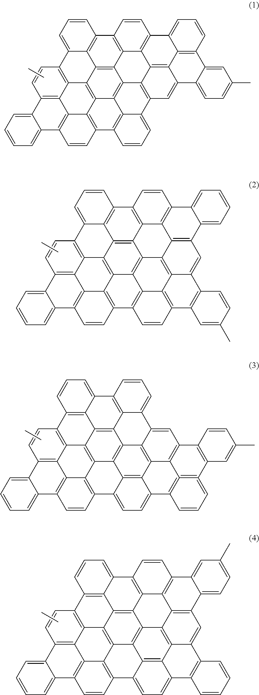
- the photoelectric conversion material contains a polymer having at least one structural unit selected from graphenes represented by the following general formulae (1) to (4).
- the photoelectric conversion material of the invention contains the ⁇ -conjugated polymer having the condensed aromatic ring structural unit.
- a ⁇ -electron cloud is spread over the ⁇ -conjugated polymer.
- the ⁇ -conjugated polymer is hereinafter referred to also as the nanographene polymer. This polymer can have a high absorbance coefficient and actively generate an exciton because the ⁇ -electron cloud spreads along the main chain.
- the polymer exhibits a small energy level difference between the HOMO and the LUMO, and thus has a narrow bandgap Eg. Therefore, the polymer has a maximum absorption wavelength shifted to the long-wavelength side, and thereby can excellently absorb a long-wavelength (near-infrared) light. Consequently, the polymer exhibits an improved sunlight utilization efficiency.
- the polymer has a LUMO energy level lower (deeper) than those of P3HT and the like. Therefore, a photoelectric conversion layer using the polymer as a donor in combination with the acceptor PCBM exhibits an energy loss lower than that of a layer using the donor P3HT. Consequently, organic photovoltaic cells using the polymer exhibit a high open circuit voltage Voc.
- the organic photovoltaic cells containing the polymer as the donor have an improved power conversion efficiency.
- the condensed aromatic rings represented by the general formulae (1) to (4) are referred to as graphenes as in Japanese Laid-Open Patent Publication No. 2007-019086.
- Nanometer-scale graphene structural units are referred to as nanographenes.
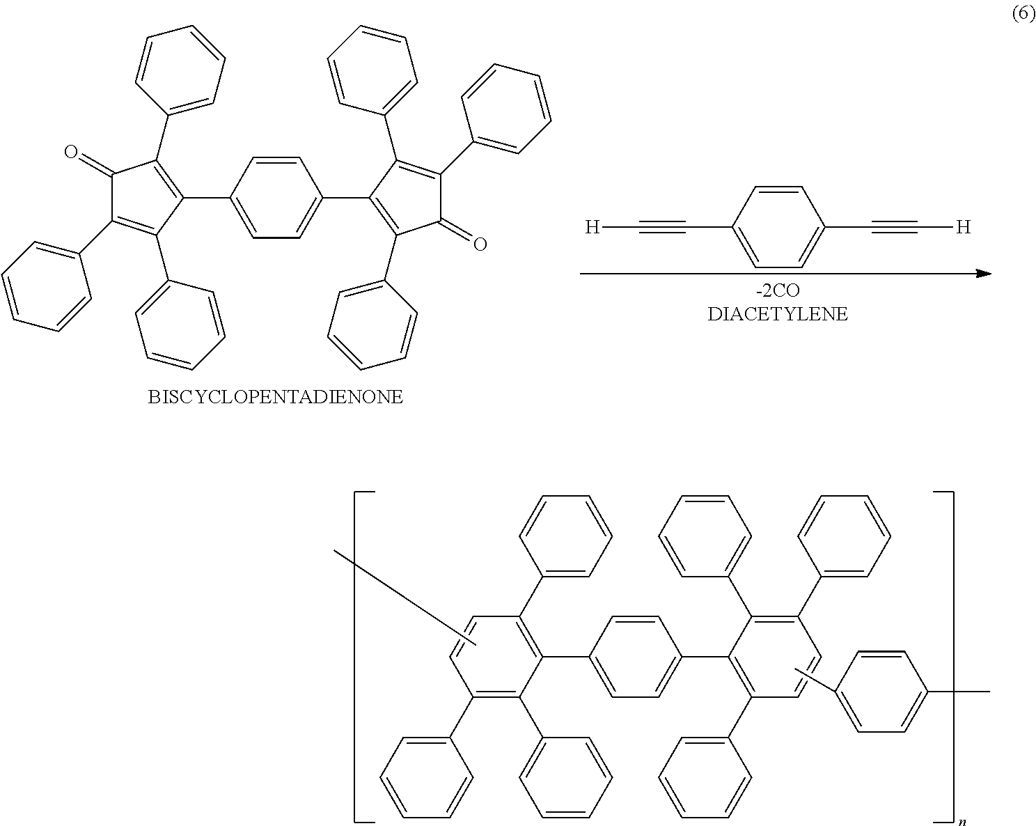
- the polymer may be a reaction product derived from a polyphenylene represented by the following general formula (5).
- the ⁇ -conjugated polymer having the condensed aromatic rings, which the ⁇ -electron cloud is sufficiently spread over, can be suitably produced by a reaction of the polyphenylene.
- the polymer preferably has a polymerization degree (the number of the structural units) of 10 to 150.
- a polymerization degree the number of the structural units
- the polymerization degree is less than 10, it is not easy to sufficiently increase the absorbance coefficient or to sufficiently lower the Eg.
- the polymerization degree is more than 150, it takes a long time to perform the polymerization, resulting in a low polymer production efficiency.
- the polymerization degree is within the above range, the polymer can be efficiently produced with an excellent donor property.
- the polymer preferably has a molecular weight of 7,400 to 111,500.
- a method for producing a photoelectric conversion material that acts as an electron donor for donating an electron or an electron acceptor for accepting an electron.
- the method contains polymerizing a phenylene derivative to prepare a polyphenylene represented by the following general formula (5) and reacting the polyphenylene to prepare a polymer having at least one structural unit selected from graphenes represented by the following general formulae (1) to (4).
- the method is capable of readily producing the polymer as the photoelectric conversion material (the donor or the acceptor).
- the polymer having the graphene structural unit can be produced by the steps of polymerizing a phenylene derivative and subjecting the obtained polyphenylene to a further reaction.
- the polymerization degree of the polymer is controlled within a range of 10 to 150 for the above reasons.
- the polymerization degree of 10 to 150 can be achieved by appropriately selecting the reaction temperature, the reaction time, or another condition in the polymerization.
- an organic photovoltaic cell using the above-described photoelectric conversion material containing the polymer.
- the organic photovoltaic cell has a photoelectric conversion layer containing the photoelectric conversion material as the electron donor.
- the photoelectric conversion layer exhibits a higher absorbance coefficient, and the donor exhibits a smaller energy level difference between the HOMO and LUMO (a narrow bandgap Eg), as compared with a cell using P3HT. Furthermore, the donor has a LUMO energy level close to that of the acceptor PCBM.
- the organic photovoltaic cell exhibits an active exciton generation property, an improved sunlight utilization efficiency, and a high open circuit voltage Voc. For these reasons, the organic photovoltaic cell has an improved power conversion efficiency.
- the organic photovoltaic cell Since the organic photovoltaic cell has a high power conversion efficiency, only a small area is required for achieving a desired power generation capacity. Therefore, the organic photovoltaic cell can have a light weight and a small load on its installation site. Furthermore, the organic photovoltaic cell can be placed in a small site, so that the layout of the solar cell can be freely designed.
- the organic photovoltaic cell is preferably a bulk heterojunction-type solar cell having a photoelectric conversion layer containing a mixture of a donor domain and an acceptor domain.
- the bulk heterojunction-type solar cell has a larger contact area between the donor and acceptor domains, as compared with a planar heterojunction-type solar cell having a donor layer and an acceptor layer separated from each other.
- the exciton is divided into the electron and hole for power generation mainly on the interface between the donor and acceptor domains. Therefore, the bulk heterojunction-type solar cell exhibits a higher power conversion efficiency due to the larger contact area.
- FIG. 1 is a schematic longitudinal cross-sectional view of a bulk heterojunction-type organic photovoltaic cell according to an embodiment of the present invention
- FIG. 2 is an explanatory view of the structural unit in a polyphenylene
- FIG. 3 is a diagram including Raman spectra of the polyphenylene and a photoelectric conversion material (a nanographene polymer derived from the polyphenylene) according to the embodiment;
- FIG. 4 is a table including properties of P3HT and the photoelectric conversion material (nanographene polymer) of the embodiment;
- FIG. 5 is an energy level diagram including the HOMO and LUMO energy levels of the photoelectric conversion material (nanographene polymer), P3HT, and PCBM;
- FIG. 6 is a structural formula of P3HT
- FIG. 7 is a structural formula of PCBM.
- FIG. 8 is a schematic explanatory view of electron transition from the HOMO of P3HT through the LUMO of P3HT to the LUMO of PCBM.
- FIG. 1 is a schematic longitudinal cross-sectional view of a principal part in a BHJ solar cell 10 according to this embodiment.
- a hole transport layer 14 In the BHJ solar cell 10 , a hole transport layer 14 , a photoelectric conversion layer 16 , and a back electrode 18 are stacked in this order on a transparent electrode 12 .
- the transparent electrode 12 acts as a positive electrode. Thus, holes 24 are transferred to the transparent electrode 12 .
- the transparent electrode 12 may be composed of a material having a sufficient transmittance of a light such as sunlight, and examples of such materials include indium-tin composite oxide (ITO).
- the hole transport layer 14 acts to accelerate the transfer of the holes 24 from the photoelectric conversion layer 16 to the transparent electrode 12 .
- the hole transport layer 14 contains a poly(3,4-ethylenedioxythiophene) doped with a polystyrene sulfonic acid, i.e. a so-called PEDOT:PSS.
- the photoelectric conversion layer 16 contains a combination of a donor domain 26 and an acceptor domain 28 .
- the donor domain 26 contains a photoelectric conversion material that acts as an electron donor
- the acceptor domain 28 contains a photoelectric conversion material that acts as an electron acceptor.
- Preferred examples of the acceptor materials include PCBM.
- the donor is a p-type semiconductor composed of a photoelectric conversion material according to the embodiment of the invention.
- the photoelectric conversion material of this embodiment contains a polymer having a structural unit selected from graphenes represented by the following general formulae (1) to (4).
- the polymer may be a reaction product derived from a polyphenylene represented by the following general formula (5) and FIG. 2 .
- a benzene ring 39 may be bonded to any one of positions 32 a and 32 b in a benzene ring 32 .
- the structural unit 30 may be selected from structural isomers.
- the structural unit 30 has such a structure that triphenylbenzene skeletons 36 and 38 are singly-bonded to a center benzene ring 34 .
- the triphenylbenzene skeletons 36 and 38 can be rotated about the single bonds to the benzene ring 34 , and the conformation of the structural unit 30 can be changed depending on the rotations.
- the structural unit 30 can have the following structures U1 to U4. Consequently, the polyphenylene contains at least one of the structures.
- the photoelectric conversion material of this embodiment is the polymer derived from the polyphenylene having the above structure as the structural unit 30 . Therefore, the structural unit (repeating unit) of the polymer depends on the structures U1 to U4 in the unreacted polyphenylene. When the structures U1 to U4 are reacted, the nanographenes represented by the following general formulae (1) to (4) are formed respectively as the structural unit of the polymer.
- the photoelectric conversion material of the embodiment is the polymer having at least one structural unit selected from the nanographenes represented by the general formulae (1) to (4).
- the polymer may contain only one type of the nanographene represented by one of the general formulae (1) to (4), and the nanographene units may be bonded to each other, but the polymer is not limited thereto.
- the polymer may be such that the nanographenes represented by the general formulae (1) to (4) are randomly bonded.
- the polymerization degree of the polymer is preferably 10 to 150.
- the polymerization degree i.e. the number of the nanographene units bonded to each other
- the polymer tends to have a low absorbance coefficient.
- the polymerization degree is more than 150, it takes a long time to perform the polymerization for producing the photoelectric conversion material, resulting in a low production efficiency.
- the photoelectric conversion material can be efficiently produced with a sufficiently improved absorbance coefficient.
- the nanographenes represented by the general formulae (1) to (4) have a molecular weight of 743.
- the polymer has a polymerization degree of 10 to 150, the polymer has a molecular weight of 7,400 to 111,500.
- the back electrode 18 is stacked on the photoelectric conversion layer 16 containing the photoelectric conversion material of the polymer.
- the back electrode 18 acts as a negative electrode, to which electrons 40 are transferred.
- the BHJ solar cell 10 of the embodiment has the above-described basic structure. Operations and advantageous effects of the BHJ solar cell 10 will be described below.
- the generated excitons 42 are moved in the donor domain 26 , and reach the interface between the donor domain 26 and the acceptor domain 28 .
- the excitons 42 are divided into the electrons 40 and the holes 24 on the interface.
- the electrons 40 are moved in the acceptor domain 28 , and reach the back electrode 18 used as the negative electrode.
- the holes 24 are moved in the donor domain 26 , are transferred through the hole transport layer 14 , and reach the transparent electrode 12 used as the positive electrode.
- the donor domain 26 in the photoelectric conversion layer 16 contains the polymer having at least one structural unit selected from the nanographenes represented by the general formulae (1) to (4).
- the ⁇ -electron cloud spreads over the entire nanographene.
- the polymer used in the donor domain 26 is a ⁇ -conjugated polymer.
- the ⁇ -electron cloud spreads over a wider area in the polymer than in the single nanographene unit (monomer).
- the polymer which has such a sufficiently spread ⁇ -electron cloud, exhibits a maximum absorption wavelength shifted to the long-wavelength side and has a high absorbance coefficient.
- the polymer exhibits a narrow bandgap (Eg) corresponding to a small energy level difference between the HOMO and LUMO. Consequently, the excitons 42 are actively generated in the donor domain 26 , resulting in a high sunlight utilization efficiency.
- the donor polymer has a LUMO energy level of about ⁇ 3.9 eV, which is deeper than that of P3HT (about ⁇ 2.5 eV).
- the LUMO energy level of the polymer is closer to that of PCBM (the fullerene derivative) in the acceptor domain 28 .
- the nanographene structural unit in the polymer is a condensed aromatic ring having an aromatic hydrocarbon skeleton, which is similar to the structure of PCBM. Consequently, the BHJ solar cell 10 exhibits a high open circuit voltage Voc.
- the BHJ solar cell 10 exhibits an excellent photoelectric power conversion efficiency because of the above properties. Therefore, only a smaller area of the BHJ solar cell 10 is required for achieving a desired power generation capacity. Consequently, the BHJ solar cell 10 can have a light weight and a small load on its installation site, so that the layout of the BHJ solar cell 10 can be designed more freely.
- a photoelectric conversion material production method according to this embodiment will be described below in relation to the production of the polymer.
- the polymer can be obtained as the reaction product derived from the polyphenylene.
- the polyphenylene can be prepared by reacting a biscyclopentadienone with a diacetylene as shown in the following reaction formula (6).
- the biscyclopentadienone can be produced by a known method. For example, 1,4-bisbenzil and dibenzyl ketone (1,3-diphenyl-2-propanone) are mixed with n-butanol to prepare a mixture solution, and a methanol solution of Triton B (benzyltrimethylammonium hydroxide) is added to the solution under heating.
- Triton B benzyltrimethylammonium hydroxide
- the polyphenylene is subjected to a reaction using a catalyst of iron chloride (FeCl 3 ).
- FeCl 3 a catalyst of iron chloride
- the polymer having the nanographene structural unit of the condensed aromatic ring represented by one of the general formulae (1) to (4) is produced as shown in the following reaction formulae (7) to (10).
- the polymer preferably has a polymerization degree of 10 to 150.
- the polymerization degree is less than 10, the absorbance coefficient is not greatly improved.
- the polymerization degree is more than 150, it takes a long time to complete the polymerization, resulting in a low polymer production efficiency.
- FIG. 3 is a diagram including Raman spectra of the polyphenylene and thus-obtained polymer. As shown in FIG. 3 , a peak of the side-chain phenyl groups is observed in the spectrum of the polyphenylene, while the peak disappears in the spectrum of the polymer. It is clear that the side-chain phenyl groups in the polyphenylene are reacted to produce the polymer having the nanographene structural unit.
- the HOMO-LUMO bandgaps Eg and the HOMO energy levels of the polymer and P3HT are shown in FIG. 4 .
- the HOMO-LUMO bandgaps Eg are obtained from absorption edges of ultraviolet-visible absorption spectra (UV-Vis), and the HOMO energy levels are measured by a photoelectron yield spectroscopic analysis (PYS).
- the polymer has a narrow bandgap Eg.
- the polymer has a bandgap Eg of 2.0 eV and a HOMO energy level of ⁇ 5.9 eV
- P3HT has a bandgap Eg of 2.2 eV and a HOMO energy level of ⁇ 4.7 eV.
- the LUMO energy levels of the polymer and P3HT are ⁇ 3.9 and ⁇ 2.5 eV respectively.
- the HOMO and LUMO energy levels of the polymer, P3HT, and PCBM are shown in FIG. 5 .
- the HOMO energy level of the polymer is lower (deeper) than that of P3HT.
- the LUMO energy level difference between the polymer and PCBM is smaller than between P3HT and PCBM.
- the BHJ solar cell 10 of this embodiment which has the photoelectric conversion layer 16 containing the polymer as the donor, exhibits a smaller energy loss and thus a higher open circuit voltage Voc, as compared with the conventional BHJ solar cell using the donor P3HT.
- the photoelectric conversion layer 16 containing the polymer may be formed as follows.
- the polymer and PCBM are separately added to an appropriate solvent such as toluene, chloroform, or chlorobenzene. Alternatively, a mixture of the polymer and PCBM may be added to the solvent. The polymer and PCBM are dissolved in the solvent to prepare a solution.
- an appropriate solvent such as toluene, chloroform, or chlorobenzene.
- a mixture of the polymer and PCBM may be added to the solvent.
- the polymer and PCBM are dissolved in the solvent to prepare a solution.
- the solution is applied onto the hole transport layer 14 by a spin coating process, an ink-jet printing process, a roll casting process, a roll-to-roll process, or the like.
- the applied solution on the hole transport layer 14 is hardened under heating, whereby the photoelectric conversion layer 16 is formed.
- the photoelectric conversion layer 16 may be subjected to an annealing treatment if necessary. In the annealing treatment, the phase separation between the donor domain 26 and the acceptor domain 28 can be further improved, and the joint interface area between the donor domain 26 and the acceptor domain 28 can be increased to improve the function.
- the photoelectric conversion layer 16 In a case where a monomer is used as the donor, it is difficult to use the above process for forming the photoelectric conversion layer 16 because of the low solubility of the monomer in the solvent.
- the polymer is used as the donor as described above. Since the polymer is soluble in the solvent, the photoelectric conversion layer 16 containing the polymer can be simply formed with ease at low cost by the above process.
- the above embodiment is described with relation to the bulk heterojunction-type organic photovoltaic cells (BHJ solar cell) 10 having the photoelectric conversion layer 16 containing the mixture of the donor and the acceptor.
- the present invention is not particularly limited thereto, and the polymer may be used in a planar heterojunction-type organic photovoltaic cell having a donor layer and an acceptor layer separated from each other. In this case, the polymer may be contained in the donor layer.
- the polymer (photoelectric conversion material) is used as the donor in the organic photovoltaic cells.
- the present invention is not particularly limited thereto, and the polymer may be used as the acceptor in the organic photovoltaic cells.
- the use of the polymer is not limited to the photoelectric conversion layer 16 in the organic photovoltaic cells.
- the polymer may be used in an optical sensor.
Landscapes
- Chemical & Material Sciences (AREA)
- Engineering & Computer Science (AREA)
- Nanotechnology (AREA)
- Materials Engineering (AREA)
- Physics & Mathematics (AREA)
- Electromagnetism (AREA)
- Health & Medical Sciences (AREA)
- Chemical Kinetics & Catalysis (AREA)
- Medicinal Chemistry (AREA)
- Polymers & Plastics (AREA)
- Organic Chemistry (AREA)
- Mathematical Physics (AREA)
- Theoretical Computer Science (AREA)
- Crystallography & Structural Chemistry (AREA)
- Polyoxymethylene Polymers And Polymers With Carbon-To-Carbon Bonds (AREA)
- Photovoltaic Devices (AREA)
Abstract

Description


Claims (12)


Applications Claiming Priority (8)
| Application Number | Priority Date | Filing Date | Title |
|---|---|---|---|
| JP2012048590 | 2012-03-05 | ||
| JP2012-048590 | 2012-03-05 | ||
| JP2012-048592 | 2012-03-05 | ||
| JP2012048592 | 2012-03-05 | ||
| JP2012-278157 | 2012-12-20 | ||
| JP2012278157A JP2013214711A (en) | 2012-03-05 | 2012-12-20 | Photoelectric conversion material, method for producing the same, and organic thin-film solar cell using the same |
| JP2012-278168 | 2012-12-20 | ||
| JP2012278168A JP2013214712A (en) | 2012-03-05 | 2012-12-20 | Photoelectric conversion material and organic thin-film solar cell using the same |
Publications (2)
| Publication Number | Publication Date |
|---|---|
| US20130228222A1 US20130228222A1 (en) | 2013-09-05 |
| US9257652B2 true US9257652B2 (en) | 2016-02-09 |
Family
ID=49042124
Family Applications (1)
| Application Number | Title | Priority Date | Filing Date |
|---|---|---|---|
| US13/778,440 Expired - Fee Related US9257652B2 (en) | 2012-03-05 | 2013-02-27 | Photoelectric conversion material, method for producing the same, and organic photovoltaic cell containing the same |
Country Status (1)
| Country | Link |
|---|---|
| US (1) | US9257652B2 (en) |
Families Citing this family (2)
| Publication number | Priority date | Publication date | Assignee | Title |
|---|---|---|---|---|
| US9276213B2 (en) * | 2012-03-05 | 2016-03-01 | Honda Motor Co., Ltd. | Photoelectric conversion material, method for producing the same, and organic photovoltaic cell containing the same |
| WO2019111603A1 (en) * | 2017-12-05 | 2019-06-13 | ソニー株式会社 | Imaging element, laminate-type imaging element, and solid-state imaging device |
Citations (9)
| Publication number | Priority date | Publication date | Assignee | Title |
|---|---|---|---|---|
| JP2007019086A (en) | 2005-07-05 | 2007-01-25 | Toyota Central Res & Dev Lab Inc | Organic semiconductor material, semiconductor device using the same, and field effect transistor |
| JP2007273939A (en) | 2005-09-06 | 2007-10-18 | Kyoto Univ | Organic thin film photoelectric conversion device and method for producing the same |
| JP4005571B2 (en) | 2004-02-04 | 2007-11-07 | 独立行政法人科学技術振興機構 | Amphiphilic hexaperihexabenzocoronene derivatives |
| WO2008056126A1 (en) | 2006-11-06 | 2008-05-15 | Carben Semicon Limited | Anisotropic semiconductor film and method of production thereof |
| JP2009231810A (en) | 2008-02-26 | 2009-10-08 | Denso Corp | Semiconductor carbon film, semiconductor device, and method of manufacturing semiconductor carbon film |
| JP2010056492A (en) | 2008-08-29 | 2010-03-11 | Japan Science & Technology Agency | Bipolar field-effect transistor where carrier mobility is tuned up |
| JP2010508667A (en) | 2006-11-07 | 2010-03-18 | スティッチング ダッチ ポリマー インスティテュート | Magnetic fluids and their use |
| US8012530B2 (en) | 2005-09-06 | 2011-09-06 | Kyoto University | Organic thin-film photoelectric conversion element and method of manufacturing the same |
| US20140323668A1 (en) * | 2011-11-18 | 2014-10-30 | Greene, Tweed & Co. | Crosslinking compounds for high glass transition temperature polymers |
-
2013
- 2013-02-27 US US13/778,440 patent/US9257652B2/en not_active Expired - Fee Related
Patent Citations (12)
| Publication number | Priority date | Publication date | Assignee | Title |
|---|---|---|---|---|
| JP4005571B2 (en) | 2004-02-04 | 2007-11-07 | 独立行政法人科学技術振興機構 | Amphiphilic hexaperihexabenzocoronene derivatives |
| JP2007019086A (en) | 2005-07-05 | 2007-01-25 | Toyota Central Res & Dev Lab Inc | Organic semiconductor material, semiconductor device using the same, and field effect transistor |
| JP2007273939A (en) | 2005-09-06 | 2007-10-18 | Kyoto Univ | Organic thin film photoelectric conversion device and method for producing the same |
| US8012530B2 (en) | 2005-09-06 | 2011-09-06 | Kyoto University | Organic thin-film photoelectric conversion element and method of manufacturing the same |
| WO2008056126A1 (en) | 2006-11-06 | 2008-05-15 | Carben Semicon Limited | Anisotropic semiconductor film and method of production thereof |
| JP2010508677A (en) | 2006-11-06 | 2010-03-18 | カーベン セミコン リミテッド | Anisotropic semiconductor film and manufacturing method thereof |
| US8124966B2 (en) | 2006-11-06 | 2012-02-28 | Carben Semicon Limited | Anisotropic semiconductor film and method of production thereof |
| US8222074B2 (en) | 2006-11-06 | 2012-07-17 | Carben Semicon Limited | Anisotropic semiconductor film and method of production thereof |
| JP2010508667A (en) | 2006-11-07 | 2010-03-18 | スティッチング ダッチ ポリマー インスティテュート | Magnetic fluids and their use |
| JP2009231810A (en) | 2008-02-26 | 2009-10-08 | Denso Corp | Semiconductor carbon film, semiconductor device, and method of manufacturing semiconductor carbon film |
| JP2010056492A (en) | 2008-08-29 | 2010-03-11 | Japan Science & Technology Agency | Bipolar field-effect transistor where carrier mobility is tuned up |
| US20140323668A1 (en) * | 2011-11-18 | 2014-10-30 | Greene, Tweed & Co. | Crosslinking compounds for high glass transition temperature polymers |
Non-Patent Citations (10)
| Title |
|---|
| Dias, Jerry Ray. A Theoretical Study of C60 Benzoids. Journal of Molecular Structure (Theochem) 1989, vol. 185, pp. 57-81. * |
| Doyz et al. Synthesis of Large Polycyclic Aromatic Hydrocarbons: Variation of Size and Periphery. Journal of the American Chemical Society 2000, vol. 122, pp. 7707-7717. * |
| Kuilla, T., et al., "Recent advances in graphene based polymer composites," Progress in Polymer Science, Jul. 27, 2010, pp. 1350-1375, vol. 35, Elsevier. |
| Office Action dated Jul. 7, 2015, issued in U.S. Appl. No. 13/778,661, U.S. Patent Office (6 pages). |
| Office Action from the Japan Patent Office dated Dec. 1, 2015, issued in counterpart Japanese Patent Application No. 2012-278157 (4 pages). |
| Office Action from the Japan Patent Office dated Dec. 1, 2015, issued in counterpart Japanese Patent Application No. 2012-278168 (3 pages). |
| Partial English Translation of Office Action from the Japan Patent Office dated Dec. 1, 2015, issued in counterpart Japanese Patent Application No. 2012-278157 (1 page). |
| Partial English Translation of Office Action from the Japan Patent Office dated Dec. 1, 2015, issued in counterpart Japanese Patent Application No. 2012-278168 (1 page). |
| Wu et al. From Branched Polyphenylenes to Graphite Ribbons. Macromolecules 2003, vol. 36, pp. 7082-7089. * |
| Wu, J., et al., "From Branched Polyphenylenses to Graphite Ribbons," Macromolecules, Aug. 19, 2003, vol. 36, pp. 7082-7089, American Chemical Society. |
Also Published As
| Publication number | Publication date |
|---|---|
| US20130228222A1 (en) | 2013-09-05 |
Similar Documents
| Publication | Publication Date | Title |
|---|---|---|
| Tang et al. | Low-bandgap n-type polymer based on a fused-DAD-type heptacyclic ring for all-polymer solar cell application with a power conversion efficiency of 10.7% | |
| Nam et al. | All-polymer solar cells with bulk heterojunction films containing electron-accepting triple bond-conjugated perylene diimide polymer | |
| Sun et al. | X-shaped oligothiophenes as a new class of electron donors for bulk-heterojunction solar cells | |
| Sun et al. | High efficiency and high V oc inverted polymer solar cells based on a low-lying HOMO polycarbazole donor and a hydrophilic polycarbazole interlayer on ITO cathode | |
| Ahmed et al. | Design of new electron acceptor materials for organic photovoltaics: synthesis, electron transport, photophysics, and photovoltaic properties of oligothiophene-functionalized naphthalene diimides | |
| Peng et al. | Enhanced solar cell performance by replacing benzodithiophene with naphthodithiophene in diketopyrrolopyrrole-based copolymers | |
| Ye et al. | 2D-conjugated benzodithiophene-based polymer acceptor: design, synthesis, nanomorphology, and photovoltaic performance | |
| Yuan et al. | Synthesis and characterization of pyrido [3, 4-b] pyrazine-based low-bandgap copolymers for bulk heterojunction solar cells | |
| Jia et al. | N-Type Self-Doped Water/Alcohol-Soluble Conjugated Polymers with Tailored Energy Levels for High-Performance Polymer Solar Cells | |
| JP6015672B2 (en) | Organic photoelectric conversion element | |
| Wang et al. | Fine-tuning of fluorinated thieno [3, 4-b] thiophene copolymer for efficient polymer solar cells | |
| US9263688B2 (en) | Photoelectric conversion material, method for producing the same, and organic photovoltaic cell containing the same | |
| JP2013131716A (en) | Organic photoelectric conversion element | |
| Chochos et al. | Synthesis of a soluble n-type cyano substituted polythiophene derivative: A potential electron acceptor in polymeric solar cells | |
| JP5845937B2 (en) | Organic photoelectric conversion element | |
| Zhao et al. | Application of biuret, dicyandiamide, or urea as a cathode buffer layer toward the efficiency enhancement of polymer solar cells | |
| Yang et al. | Comparison of three n-type copolymers based on benzodithiophene and naphthalene diimide/perylene diimide/fused perylene diimides for all-polymer solar cells application | |
| Chen et al. | Dibenzothiophene-S, S-dioxide and bispyridinium-based cationic polyfluorene derivative as an efficient cathode modifier for polymer solar cells | |
| Liu et al. | A rational design and synthesis of cross-conjugated small molecule acceptors approaching high-performance fullerene-free polymer solar cells | |
| JP2014053383A (en) | Tandem organic photoelectric conversion element and solar cell using the same | |
| Chen et al. | 1, 4-di (3-alkoxy-2-thienyl)-2, 5-difluorophenylene: A building block enabling high-performance polymer semiconductors with increased open-circuit voltages | |
| Chou et al. | Naphthobisthiadiazole-Based π-Conjugated Polymers for Nonfullerene Solar Cells: Suppressing Intermolecular Interaction Improves Photovoltaic Performance | |
| US9145468B2 (en) | Photoelectric conversion material, method for producing the same, and organic photovoltaic cell containing the same | |
| Wahalathantrige Don et al. | Vinyl-flanked diketopyrrolopyrrole polymer/MoS2 hybrid for donor–acceptor semiconductor photodetection | |
| JP5853805B2 (en) | Conjugated polymer compound and organic photoelectric conversion device using the same |
Legal Events
| Date | Code | Title | Description |
|---|---|---|---|
| AS | Assignment |
Owner name: HONDA MOTOR CO., LTD., JAPAN Free format text: ASSIGNMENT OF ASSIGNORS INTEREST;ASSIGNORS:SHIBA, TADAHIRO;MIURA, KAZUHIRO;REEL/FRAME:029885/0377 Effective date: 20130201 |
|
| FEPP | Fee payment procedure |
Free format text: PAYOR NUMBER ASSIGNED (ORIGINAL EVENT CODE: ASPN); ENTITY STATUS OF PATENT OWNER: LARGE ENTITY |
|
| STCF | Information on status: patent grant |
Free format text: PATENTED CASE |
|
| MAFP | Maintenance fee payment |
Free format text: PAYMENT OF MAINTENANCE FEE, 4TH YEAR, LARGE ENTITY (ORIGINAL EVENT CODE: M1551); ENTITY STATUS OF PATENT OWNER: LARGE ENTITY Year of fee payment: 4 |
|
| FEPP | Fee payment procedure |
Free format text: MAINTENANCE FEE REMINDER MAILED (ORIGINAL EVENT CODE: REM.); ENTITY STATUS OF PATENT OWNER: LARGE ENTITY |
|
| LAPS | Lapse for failure to pay maintenance fees |
Free format text: PATENT EXPIRED FOR FAILURE TO PAY MAINTENANCE FEES (ORIGINAL EVENT CODE: EXP.); ENTITY STATUS OF PATENT OWNER: LARGE ENTITY |
|
| STCH | Information on status: patent discontinuation |
Free format text: PATENT EXPIRED DUE TO NONPAYMENT OF MAINTENANCE FEES UNDER 37 CFR 1.362 |
|
| FP | Lapsed due to failure to pay maintenance fee |
Effective date: 20240209 |