US9257530B1 - Methods of making integrated circuits and components thereof - Google Patents
Methods of making integrated circuits and components thereof Download PDFInfo
- Publication number
- US9257530B1 US9257530B1 US14/471,660 US201414471660A US9257530B1 US 9257530 B1 US9257530 B1 US 9257530B1 US 201414471660 A US201414471660 A US 201414471660A US 9257530 B1 US9257530 B1 US 9257530B1
- Authority
- US
- United States
- Prior art keywords
- gate structure
- source
- semiconductor substrate
- silicon oxide
- ultra low
- Prior art date
- Legal status (The legal status is an assumption and is not a legal conclusion. Google has not performed a legal analysis and makes no representation as to the accuracy of the status listed.)
- Expired - Fee Related
Links
Images


Classifications
-
- H01L29/66545—
-
- H—ELECTRICITY
- H10—SEMICONDUCTOR DEVICES; ELECTRIC SOLID-STATE DEVICES NOT OTHERWISE PROVIDED FOR
- H10D—INORGANIC ELECTRIC SEMICONDUCTOR DEVICES
- H10D64/00—Electrodes of devices having potential barriers
- H10D64/01—Manufacture or treatment
- H10D64/017—Manufacture or treatment using dummy gates in processes wherein at least parts of the final gates are self-aligned to the dummy gates, i.e. replacement gate processes
-
- H01L21/283—
-
- H—ELECTRICITY
- H10—SEMICONDUCTOR DEVICES; ELECTRIC SOLID-STATE DEVICES NOT OTHERWISE PROVIDED FOR
- H10D—INORGANIC ELECTRIC SEMICONDUCTOR DEVICES
- H10D30/00—Field-effect transistors [FET]
- H10D30/01—Manufacture or treatment
- H10D30/021—Manufacture or treatment of FETs having insulated gates [IGFET]
- H10D30/027—Manufacture or treatment of FETs having insulated gates [IGFET] of lateral single-gate IGFETs
- H10D30/0273—Manufacture or treatment of FETs having insulated gates [IGFET] of lateral single-gate IGFETs forming final gates or dummy gates after forming source and drain electrodes, e.g. contact first technology
-
- H—ELECTRICITY
- H10—SEMICONDUCTOR DEVICES; ELECTRIC SOLID-STATE DEVICES NOT OTHERWISE PROVIDED FOR
- H10P—GENERIC PROCESSES OR APPARATUS FOR THE MANUFACTURE OR TREATMENT OF DEVICES COVERED BY CLASS H10
- H10P14/00—Formation of materials, e.g. in the shape of layers or pillars
- H10P14/40—Formation of materials, e.g. in the shape of layers or pillars of conductive or resistive materials
-
- H—ELECTRICITY
- H10—SEMICONDUCTOR DEVICES; ELECTRIC SOLID-STATE DEVICES NOT OTHERWISE PROVIDED FOR
- H10W—GENERIC PACKAGES, INTERCONNECTIONS, CONNECTORS OR OTHER CONSTRUCTIONAL DETAILS OF DEVICES COVERED BY CLASS H10
- H10W20/00—Interconnections in chips, wafers or substrates
- H10W20/01—Manufacture or treatment
- H10W20/031—Manufacture or treatment of conductive parts of the interconnections
- H10W20/063—Manufacture or treatment of conductive parts of the interconnections by forming conductive members before forming protective insulating material
-
- H—ELECTRICITY
- H10—SEMICONDUCTOR DEVICES; ELECTRIC SOLID-STATE DEVICES NOT OTHERWISE PROVIDED FOR
- H10D—INORGANIC ELECTRIC SEMICONDUCTOR DEVICES
- H10D64/00—Electrodes of devices having potential barriers
- H10D64/01—Manufacture or treatment
- H10D64/011—Manufacture or treatment of electrodes ohmically coupled to a semiconductor
- H10D64/0111—Manufacture or treatment of electrodes ohmically coupled to a semiconductor to Group IV semiconductors
- H10D64/0112—Manufacture or treatment of electrodes ohmically coupled to a semiconductor to Group IV semiconductors using conductive layers comprising silicides
-
- H—ELECTRICITY
- H10—SEMICONDUCTOR DEVICES; ELECTRIC SOLID-STATE DEVICES NOT OTHERWISE PROVIDED FOR
- H10D—INORGANIC ELECTRIC SEMICONDUCTOR DEVICES
- H10D64/00—Electrodes of devices having potential barriers
- H10D64/60—Electrodes characterised by their materials
- H10D64/66—Electrodes having a conductor capacitively coupled to a semiconductor by an insulator, e.g. MIS electrodes
- H10D64/68—Electrodes having a conductor capacitively coupled to a semiconductor by an insulator, e.g. MIS electrodes characterised by the insulator, e.g. by the gate insulator
- H10D64/691—Electrodes having a conductor capacitively coupled to a semiconductor by an insulator, e.g. MIS electrodes characterised by the insulator, e.g. by the gate insulator comprising metallic compounds, e.g. metal oxides or metal silicates
-
- H—ELECTRICITY
- H10—SEMICONDUCTOR DEVICES; ELECTRIC SOLID-STATE DEVICES NOT OTHERWISE PROVIDED FOR
- H10W—GENERIC PACKAGES, INTERCONNECTIONS, CONNECTORS OR OTHER CONSTRUCTIONAL DETAILS OF DEVICES COVERED BY CLASS H10
- H10W20/00—Interconnections in chips, wafers or substrates
- H10W20/01—Manufacture or treatment
- H10W20/071—Manufacture or treatment of dielectric parts thereof
- H10W20/081—Manufacture or treatment of dielectric parts thereof by forming openings in the dielectric parts
-
- H—ELECTRICITY
- H10—SEMICONDUCTOR DEVICES; ELECTRIC SOLID-STATE DEVICES NOT OTHERWISE PROVIDED FOR
- H10W—GENERIC PACKAGES, INTERCONNECTIONS, CONNECTORS OR OTHER CONSTRUCTIONAL DETAILS OF DEVICES COVERED BY CLASS H10
- H10W20/00—Interconnections in chips, wafers or substrates
- H10W20/40—Interconnections external to wafers or substrates, e.g. back-end-of-line [BEOL] metallisations or vias connecting to gate electrodes
Definitions
- the technical field generally relates to methods of making integrated circuits and, more particularly, to methods of making integrated circuits with minimized parasitic capacitance.
- MOSFETs metal oxide semiconductor field effect transistors
- a MOS transistor includes a gate electrode as a control electrode overlying a semiconductor substrate and spaced-apart source and drain regions in the substrate between which a current can flow.
- a gate insulator is disposed between the gate electrode and the semiconductor substrate to electrically isolate the gate electrode from the substrate.
- a control voltage applied to the gate electrode through a gate contact controls the flow of current through a channel in the substrate underlying the gate electrode between the source and drain regions.
- One exemplary embodiment provides a method of making an integrated circuit.
- the method includes forming a dummy gate structure above a semiconductor substrate, etching an exposed semiconductor substrate outside the dummy gate structure, depositing silicon oxide over the dummy gate structure and the semiconductor substrate to form a silicon oxide layer, etching source and drain contact vias through the silicon oxide layer, implanting source and drain dopants through the source and drain contact vias, removing the dummy gate structure, forming a final gate structure, etching substantially all of the silicon oxide layer, and depositing an ultra low K dielectric to form an ultra low K dielectric layer.
- Another exemplary embodiment provides a method of making an integrated circuit.
- the method includes providing a semiconductor substrate having a dummy gate structure disposed thereon, depositing a silicon oxide layer over the dummy gate structure and the semiconductor substrate to form a silicon oxide layer, etching substantially all of the silicon oxide layer, and depositing an ultra low K dielectric to form an ultra low K dielectric layer.
- Yet another exemplary embodiment provides a method of making an integrated circuit.
- the method includes providing a semiconductor substrate with a dummy gate structure formed thereon and a silicon oxide layer covering the dummy gate structure and the semiconductor substrate, etching source and drain contact vias through the silicon oxide layer, implanting source and drain dopants through the source and drain contact vias, annealing after implanting, forming a silicide region in the source and drain contact vias, removing the dummy gate structure, forming a final gate structure, etching substantially all of the silicon oxide layer, and depositing an ultra low K dielectric to form an ultra low K dielectric layer.
- FIGS. 1-5 illustrate, in cross section, a method of making an integrated circuit in accordance with an exemplary embodiment.
- semiconductor substrate is used to encompass a substrate that includes one or more individual layers of semiconductor materials conventionally used in the semiconductor industry from which to make electrical devices.
- semiconductor material includes monocrystalline silicon materials typically used in the semiconductor industry, as well as polycrystalline silicon materials, and silicon admixed with other elements such as germanium, carbon, and the like.
- semiconductor material encompasses other materials such as relatively pure and impurity-doped germanium, gallium arsenide, zinc oxide, glass, and the like.
- the semiconductor material is preferably a silicon substrate.
- the semiconductor substrate may be a bulk semiconductor wafer or may be a thin layer of semiconductor on an insulating layer (commonly known as silicon-on-insulator or SOI) that, in turn, is supported by a carrier wafer.
- SOI silicon-on-insulator
- overlying means “over” and “on,” wherein “on” means in direct physical contact and “over” means that another layer may be interposed therebetween.
- N-channel field effect transistor may be abbreviated “NFET”.
- P-channel field effect transistor may be abbreviated “PFET”.
- transistor As used herein, the terms “transistor”, “device”, and “integrated circuit” may be used interchangeably.
- the embodiments disclosed herein overcome shortcomings by using an integration scheme that allows replacement of standard spacer material with ultralow dielectric coefficient (ULK) material.
- ULK ultralow dielectric coefficient
- FIGS. 1-5 depict an illustrative example wherein the methods disclosed herein may be employed when the various devices are formed using so-called “replacement gate” (RMG) or “gate-last” techniques.
- RMG replacement gate
- the replacement gate technique involves forming an integrated circuit with a sacrificial gate structure, including the formation of source and drain regions and metal silicide contact regions, and thereafter removing the sacrificial gate structure and replacing it with a final gate structure that typically includes at least one layer of metal or other electrically conductive material.
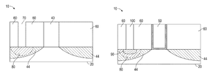
- the integrated circuit 10 includes a semiconductor substrate 20 with a dummy gate structure or dummy gate 40 formed thereon, or positioned over the semiconductor substrate 20 .
- the integrated circuit 10 may be a complementary metal oxide semiconductor (CMOS) device.
- CMOS complementary metal oxide semiconductor
- the basic structures have been formed. More specifically, at the point of fabrication depicted in FIG. 1 , the sacrificial gate or dummy gate structure 40 that is formed as part of the process has been formed.
- the sacrificial structure 40 typically includes a sacrificial or dummy gate insulation layer, a dummy or sacrificial gate electrode, and a protective gate cap layer.
- the dummy gate insulation layer may be incorporated into the final device.
- the various components and structures of the integrated circuit 10 may be formed using a variety of different materials and by performing a variety of known techniques.
- the sacrificial gate insulation layer may include silicon oxide and the sacrificial gate electrode may include a polysilicon.
- an exposed portion of the semiconductor substrate 20 outside the dummy gate structure 40 is etched, typically about 5 to about 10 nanometers.
- an epitaxial region 44 is formed by epitaxially growing semiconductor material.
- the semiconductor material is in situ doped with source and drain dopants.
- the epitaxial region 44 may be doped after formation. Examples of suitable dopants include, but are not limited to, arsenic, boron, and phosphorus. Such an epitaxial deposition process is performed so as to form the epitaxial region 44 as an embedded stressor material.
- silicon oxide is deposited to form a silicon oxide layer 60 over the dummy gate structure 40 and the semiconductor substrate 20 .
- the silicon oxide layer 60 can be any suitable thickness, such as about 30 to about 100 nanometers, and is deposited using any suitable process, such as chemical vapor deposition (CVD).
- the silicon dioxide layer 60 can have superior dopant blocking capabilities as compared to, e.g., a ULK material.
- the silicon dioxide layer 60 can prevent unwanted dopant implantation and corresponding increase in K value in regions outside the desired doped area. That being done, the silicon oxide layer 60 undergoes chemical-mechanical polishing to remove extraneous materials.
- a source and drain or implanted dopant region 80 is formed by implanting dopant material, such as N-type dopants for NFET devices and P-type dopants for PFET devices, into the semiconductor substrate 20 . These dopants are implanted into the semiconductor substrate 20 using known masking and ion implantation techniques.
- N-type dopants include phosphorus or arsenic
- P-type dopants include boron, aluminum, gallium, or indium.
- annealing typically follows. The annealing is typically a diffusionless process, and serves to activate dopants and repair lattice damage where an optional heat treating process may not have been previously performed.
- a silicide region 90 is formed in the source and drain contact vias 70 and the source and drain contact vias 70 are filled with a source/drain contact material to form a source/drain contact 100 .
- the silicide region may include any one of several well-known refractory metal-based silicide materials, such as nickel silicide or cobalt silicide, and may be formed by using techniques and processing steps, such as depositing a refractory metal layer, performing a thermal treatment to cause a chemical reaction between the refractory metal layer and the underlying semiconductor materials of the semiconductor substrate 20 .
- the source/drain contact 100 includes tungsten.
- the dimensions of the source/drain contact 100 and its position may vary depending on the technology node, and can follow standards consistent with the assessment of the International Technology Roadmap for Semiconductors.
- the dummy gate structure 40 is removed and replaced with a final gate structure 50 using any suitable process, such as a replacement metal gate process. Particularly, one or more etching processes are performed to remove the dummy gate without damaging the silicon oxide layer 60 to thereby define a gate cavity with a replacement gate subsequently formed therein.
- the remaining silicon oxide layer 60 is etched and removed, and an ultra low K dielectric is deposited using any suitable process, such as a plasma enhanced chemical vapor deposition process, to form an ultra low K dielectric layer 110 .
- the ultra low K dielectric layer 110 has a K value of no more than about 2.7.
- the ultra low K dielectric layer 110 or layers are formed with various precursors and a silicon, an oxygen and a methyl and methylene gas mix.
- a porous silicon oxide layer contains at least some carbon, and has a K value of no more than about 2.7.
- chemical mechanical polishing follows and standard back end of line fabrication is conducted to complete manufacture of the integrated circuit.
- the embodiments disclosed herein are applicable for planar and three dimensional device architectures, such as a fin-based or wire-based multi-gate transistors using a replacement gate integration scheme. Moreover, the embodiments are applicable to highly scaled device architectures, such as about 28 nanometers, or even about 14 nanometers, or less, and applicable to large variety of substrate materials.
Landscapes
- Insulated Gate Type Field-Effect Transistor (AREA)
- Electrodes Of Semiconductors (AREA)
Abstract
Description
Claims (20)
Priority Applications (1)
| Application Number | Priority Date | Filing Date | Title |
|---|---|---|---|
| US14/471,660 US9257530B1 (en) | 2014-08-28 | 2014-08-28 | Methods of making integrated circuits and components thereof |
Applications Claiming Priority (1)
| Application Number | Priority Date | Filing Date | Title |
|---|---|---|---|
| US14/471,660 US9257530B1 (en) | 2014-08-28 | 2014-08-28 | Methods of making integrated circuits and components thereof |
Publications (2)
| Publication Number | Publication Date |
|---|---|
| US9257530B1 true US9257530B1 (en) | 2016-02-09 |
| US20160064515A1 US20160064515A1 (en) | 2016-03-03 |
Family
ID=55235664
Family Applications (1)
| Application Number | Title | Priority Date | Filing Date |
|---|---|---|---|
| US14/471,660 Expired - Fee Related US9257530B1 (en) | 2014-08-28 | 2014-08-28 | Methods of making integrated circuits and components thereof |
Country Status (1)
| Country | Link |
|---|---|
| US (1) | US9257530B1 (en) |
Cited By (2)
| Publication number | Priority date | Publication date | Assignee | Title |
|---|---|---|---|---|
| US9608112B2 (en) * | 2015-08-03 | 2017-03-28 | Globalfoundries Inc. | BULEX contacts in advanced FDSOI techniques |
| US9698179B2 (en) | 2015-08-03 | 2017-07-04 | Globalfoundries Inc. | Capacitor structure and method of forming a capacitor structure |
Citations (6)
| Publication number | Priority date | Publication date | Assignee | Title |
|---|---|---|---|---|
| US20110241200A1 (en) | 2010-04-05 | 2011-10-06 | International Business Machines Corporation | Ultra low dielectric constant material with enhanced mechanical properties |
| US20130178024A1 (en) | 2012-01-09 | 2013-07-11 | Globalfoundries Inc. | In Situ Doping and Diffusionless Annealing of Embedded Stressor Regions in PMOS and NMOS Devices |
| US20140027859A1 (en) | 2012-07-30 | 2014-01-30 | Globalfoundries Inc. | Methods of forming transistor devices with high-k insulation layers and the resulting devices |
| US20140084486A1 (en) | 2009-09-28 | 2014-03-27 | Globalfoundries Singapore Pte. Ltd. | Reliable interconnect for semiconductor device |
| US20140098459A1 (en) | 2012-10-10 | 2014-04-10 | GlobalFoundries, Inc. | Capacitor and contact structures, and formation processes thereof |
| US20140273386A1 (en) * | 2013-03-14 | 2014-09-18 | United Microelectronics Corp. | Method of forming metal silicide layer |
-
2014
- 2014-08-28 US US14/471,660 patent/US9257530B1/en not_active Expired - Fee Related
Patent Citations (6)
| Publication number | Priority date | Publication date | Assignee | Title |
|---|---|---|---|---|
| US20140084486A1 (en) | 2009-09-28 | 2014-03-27 | Globalfoundries Singapore Pte. Ltd. | Reliable interconnect for semiconductor device |
| US20110241200A1 (en) | 2010-04-05 | 2011-10-06 | International Business Machines Corporation | Ultra low dielectric constant material with enhanced mechanical properties |
| US20130178024A1 (en) | 2012-01-09 | 2013-07-11 | Globalfoundries Inc. | In Situ Doping and Diffusionless Annealing of Embedded Stressor Regions in PMOS and NMOS Devices |
| US20140027859A1 (en) | 2012-07-30 | 2014-01-30 | Globalfoundries Inc. | Methods of forming transistor devices with high-k insulation layers and the resulting devices |
| US20140098459A1 (en) | 2012-10-10 | 2014-04-10 | GlobalFoundries, Inc. | Capacitor and contact structures, and formation processes thereof |
| US20140273386A1 (en) * | 2013-03-14 | 2014-09-18 | United Microelectronics Corp. | Method of forming metal silicide layer |
Cited By (2)
| Publication number | Priority date | Publication date | Assignee | Title |
|---|---|---|---|---|
| US9608112B2 (en) * | 2015-08-03 | 2017-03-28 | Globalfoundries Inc. | BULEX contacts in advanced FDSOI techniques |
| US9698179B2 (en) | 2015-08-03 | 2017-07-04 | Globalfoundries Inc. | Capacitor structure and method of forming a capacitor structure |
Also Published As
| Publication number | Publication date |
|---|---|
| US20160064515A1 (en) | 2016-03-03 |
Similar Documents
| Publication | Publication Date | Title |
|---|---|---|
| US20220352151A1 (en) | Method of manufacturing semiconductor device | |
| US9899517B2 (en) | Dislocation stress memorization technique (DSMT) on epitaxial channel devices | |
| US8003454B2 (en) | CMOS process with optimized PMOS and NMOS transistor devices | |
| US8546228B2 (en) | Strained thin body CMOS device having vertically raised source/drain stressors with single spacer | |
| US9023713B2 (en) | Ultrathin body fully depleted silicon-on-insulator integrated circuits and methods for fabricating same | |
| US20170154900A1 (en) | Integrated tensile strained silicon nfet and compressive strained silicon-germanium pfet implemented in finfet technology | |
| US20120276695A1 (en) | Strained thin body CMOS with Si:C and SiGe stressor | |
| US9263587B1 (en) | Fin device with blocking layer in channel region | |
| US20090289280A1 (en) | Method for Making Transistors and the Device Thereof | |
| US9502564B2 (en) | Fully depleted device with buried insulating layer in channel region | |
| US10453921B2 (en) | Semiconductor structure and fabrication method thereof | |
| US20110108894A1 (en) | Method of forming strained structures in semiconductor devices | |
| KR20220005402A (en) | Selective silicon etch for gate all around transistors | |
| US9299616B1 (en) | Integrated circuits with separate workfunction material layers and methods for fabricating the same | |
| US9460957B2 (en) | Method and structure for nitrogen-doped shallow-trench isolation dielectric | |
| US20140357028A1 (en) | Methods for fabricating integrated circuits with the implantation of fluorine | |
| US9257530B1 (en) | Methods of making integrated circuits and components thereof | |
| US9472465B2 (en) | Methods of fabricating integrated circuits | |
| US20130295767A1 (en) | Increased transistor performance by implementing an additional cleaning process in a stress liner approach | |
| US20160064286A1 (en) | Integrated circuits and methods for fabricating integrated circuits | |
| US8872272B2 (en) | Stress enhanced CMOS circuits and methods for their manufacture | |
| KR102959338B1 (en) | METHOD FOR MANUFACTURING A SeOI INTEGRATED CIRCUIT CHIP | |
| US11387364B2 (en) | Transistor with phase transition material region between channel region and each source/drain region | |
| CN103000522B (en) | Method for manufacturing NMOS (N-channel metal oxide semiconductor) transistor |
Legal Events
| Date | Code | Title | Description |
|---|---|---|---|
| AS | Assignment |
Owner name: GLOBALFOUNDRIES, INC., CAYMAN ISLANDS Free format text: ASSIGNMENT OF ASSIGNORS INTEREST;ASSIGNORS:ZSCHATSCH, GERD;FLACHOWSKY, STEFAN;HOENTSCHEL, JAN;SIGNING DATES FROM 20140803 TO 20140825;REEL/FRAME:033631/0819 |
|
| STCF | Information on status: patent grant |
Free format text: PATENTED CASE |
|
| AS | Assignment |
Owner name: WILMINGTON TRUST, NATIONAL ASSOCIATION, DELAWARE Free format text: SECURITY AGREEMENT;ASSIGNOR:GLOBALFOUNDRIES INC.;REEL/FRAME:049490/0001 Effective date: 20181127 |
|
| FEPP | Fee payment procedure |
Free format text: MAINTENANCE FEE REMINDER MAILED (ORIGINAL EVENT CODE: REM.); ENTITY STATUS OF PATENT OWNER: LARGE ENTITY |
|
| LAPS | Lapse for failure to pay maintenance fees |
Free format text: PATENT EXPIRED FOR FAILURE TO PAY MAINTENANCE FEES (ORIGINAL EVENT CODE: EXP.); ENTITY STATUS OF PATENT OWNER: LARGE ENTITY |
|
| STCH | Information on status: patent discontinuation |
Free format text: PATENT EXPIRED DUE TO NONPAYMENT OF MAINTENANCE FEES UNDER 37 CFR 1.362 |
|
| FP | Lapsed due to failure to pay maintenance fee |
Effective date: 20200209 |
|
| AS | Assignment |
Owner name: GLOBALFOUNDRIES INC., CAYMAN ISLANDS Free format text: RELEASE BY SECURED PARTY;ASSIGNOR:WILMINGTON TRUST, NATIONAL ASSOCIATION;REEL/FRAME:054636/0001 Effective date: 20201117 |
|
| AS | Assignment |
Owner name: GLOBALFOUNDRIES U.S. INC., NEW YORK Free format text: RELEASE BY SECURED PARTY;ASSIGNOR:WILMINGTON TRUST, NATIONAL ASSOCIATION;REEL/FRAME:056987/0001 Effective date: 20201117 Owner name: GLOBALFOUNDRIES U.S. INC., NEW YORK Free format text: RELEASE OF SECURITY INTEREST;ASSIGNOR:WILMINGTON TRUST, NATIONAL ASSOCIATION;REEL/FRAME:056987/0001 Effective date: 20201117 |