US9250709B2 - Secure point of sale terminal - Google Patents
Secure point of sale terminal Download PDFInfo
- Publication number
- US9250709B2 US9250709B2 US14/592,296 US201514592296A US9250709B2 US 9250709 B2 US9250709 B2 US 9250709B2 US 201514592296 A US201514592296 A US 201514592296A US 9250709 B2 US9250709 B2 US 9250709B2
- Authority
- US
- United States
- Prior art keywords
- tampering
- electrical
- enclosure
- key
- substrate
- Prior art date
- Legal status (The legal status is an assumption and is not a legal conclusion. Google has not performed a legal analysis and makes no representation as to the accuracy of the status listed.)
- Active
Links
- 238000013479 data entry Methods 0.000 claims abstract description 49
- 239000004020 conductor Substances 0.000 claims description 120
- 239000000758 substrate Substances 0.000 claims description 51
- 238000001514 detection method Methods 0.000 claims description 22
- 230000002093 peripheral effect Effects 0.000 description 28
- 230000001681 protective effect Effects 0.000 description 21
- 230000000994 depressogenic effect Effects 0.000 description 17
- 239000004033 plastic Substances 0.000 description 12
- 230000013011 mating Effects 0.000 description 11
- OKTJSMMVPCPJKN-UHFFFAOYSA-N Carbon Chemical compound [C] OKTJSMMVPCPJKN-UHFFFAOYSA-N 0.000 description 4
- 238000003491 array Methods 0.000 description 4
- 229910052799 carbon Inorganic materials 0.000 description 4
- 239000002184 metal Substances 0.000 description 4
- ORQBXQOJMQIAOY-UHFFFAOYSA-N nobelium Chemical compound [No] ORQBXQOJMQIAOY-UHFFFAOYSA-N 0.000 description 4
- 238000005476 soldering Methods 0.000 description 2
- 238000005553 drilling Methods 0.000 description 1
- 239000003292 glue Substances 0.000 description 1
- 238000002347 injection Methods 0.000 description 1
- 239000007924 injection Substances 0.000 description 1
- 238000012986 modification Methods 0.000 description 1
- 230000004048 modification Effects 0.000 description 1
- 238000003825 pressing Methods 0.000 description 1
Images


Classifications
-
- G—PHYSICS
- G06—COMPUTING; CALCULATING OR COUNTING
- G06F—ELECTRIC DIGITAL DATA PROCESSING
- G06F21/00—Security arrangements for protecting computers, components thereof, programs or data against unauthorised activity
- G06F21/70—Protecting specific internal or peripheral components, in which the protection of a component leads to protection of the entire computer
- G06F21/82—Protecting input, output or interconnection devices
- G06F21/83—Protecting input, output or interconnection devices input devices, e.g. keyboards, mice or controllers thereof
-
- G—PHYSICS
- G06—COMPUTING; CALCULATING OR COUNTING
- G06F—ELECTRIC DIGITAL DATA PROCESSING
- G06F1/00—Details not covered by groups G06F3/00 - G06F13/00 and G06F21/00
- G06F1/16—Constructional details or arrangements
- G06F1/1613—Constructional details or arrangements for portable computers
- G06F1/1626—Constructional details or arrangements for portable computers with a single-body enclosure integrating a flat display, e.g. Personal Digital Assistants [PDAs]
-
- G—PHYSICS
- G06—COMPUTING; CALCULATING OR COUNTING
- G06F—ELECTRIC DIGITAL DATA PROCESSING
- G06F1/00—Details not covered by groups G06F3/00 - G06F13/00 and G06F21/00
- G06F1/16—Constructional details or arrangements
- G06F1/1613—Constructional details or arrangements for portable computers
- G06F1/1633—Constructional details or arrangements of portable computers not specific to the type of enclosures covered by groups G06F1/1615 - G06F1/1626
- G06F1/1656—Details related to functional adaptations of the enclosure, e.g. to provide protection against EMI, shock, water, or to host detachable peripherals like a mouse or removable expansions units like PCMCIA cards, or to provide access to internal components for maintenance or to removable storage supports like CDs or DVDs, or to mechanically mount accessories
- G06F1/1658—Details related to functional adaptations of the enclosure, e.g. to provide protection against EMI, shock, water, or to host detachable peripherals like a mouse or removable expansions units like PCMCIA cards, or to provide access to internal components for maintenance or to removable storage supports like CDs or DVDs, or to mechanically mount accessories related to the mounting of internal components, e.g. disc drive or any other functional module
-
- G—PHYSICS
- G06—COMPUTING; CALCULATING OR COUNTING
- G06F—ELECTRIC DIGITAL DATA PROCESSING
- G06F1/00—Details not covered by groups G06F3/00 - G06F13/00 and G06F21/00
- G06F1/16—Constructional details or arrangements
- G06F1/1613—Constructional details or arrangements for portable computers
- G06F1/1633—Constructional details or arrangements of portable computers not specific to the type of enclosures covered by groups G06F1/1615 - G06F1/1626
- G06F1/1684—Constructional details or arrangements related to integrated I/O peripherals not covered by groups G06F1/1635 - G06F1/1675
-
- G—PHYSICS
- G06—COMPUTING; CALCULATING OR COUNTING
- G06F—ELECTRIC DIGITAL DATA PROCESSING
- G06F21/00—Security arrangements for protecting computers, components thereof, programs or data against unauthorised activity
- G06F21/70—Protecting specific internal or peripheral components, in which the protection of a component leads to protection of the entire computer
- G06F21/86—Secure or tamper-resistant housings
-
- G—PHYSICS
- G06—COMPUTING; CALCULATING OR COUNTING
- G06F—ELECTRIC DIGITAL DATA PROCESSING
- G06F3/00—Input arrangements for transferring data to be processed into a form capable of being handled by the computer; Output arrangements for transferring data from processing unit to output unit, e.g. interface arrangements
- G06F3/01—Input arrangements or combined input and output arrangements for interaction between user and computer
- G06F3/02—Input arrangements using manually operated switches, e.g. using keyboards or dials
- G06F3/0202—Constructional details or processes of manufacture of the input device
- G06F3/0219—Special purpose keyboards
-
- G—PHYSICS
- G06—COMPUTING; CALCULATING OR COUNTING
- G06F—ELECTRIC DIGITAL DATA PROCESSING
- G06F3/00—Input arrangements for transferring data to be processed into a form capable of being handled by the computer; Output arrangements for transferring data from processing unit to output unit, e.g. interface arrangements
- G06F3/01—Input arrangements or combined input and output arrangements for interaction between user and computer
- G06F3/02—Input arrangements using manually operated switches, e.g. using keyboards or dials
- G06F3/023—Arrangements for converting discrete items of information into a coded form, e.g. arrangements for interpreting keyboard generated codes as alphanumeric codes, operand codes or instruction codes
-
- H—ELECTRICITY
- H04—ELECTRIC COMMUNICATION TECHNIQUE
- H04M—TELEPHONIC COMMUNICATION
- H04M1/00—Substation equipment, e.g. for use by subscribers
- H04M1/02—Constructional features of telephone sets
- H04M1/23—Construction or mounting of dials or of equivalent devices; Means for facilitating the use thereof
Definitions
- the present invention relates generally to secure keypad devices and more particularly to data entry devices having anti-tamper functionality.
- the present invention seeks to provide improved secure keypad devices.
- a data entry device including a housing formed of at least two portions, data entry circuitry located within the housing, at least one case-open switch assembly operative to sense when the housing is opened and tamper indication circuitry operative to receive an input from the at least one case-open switch assembly and to provide an output indication of possible tampering with the data entry circuitry located within the housing,
- the at least one case-open switch assembly including an arrangement of electrical contacts including at least first, second and third contacts and a displaceable conductive element, which defines a short circuit between the first and second contacts only when the housing is closed, the third contact being arranged between the first and second contacts and the displaceable conductive element so as to normally not be short circuited to the first and second contacts when the housing is closed, the tamper indication circuitry and the third contact together being operative such that when the third contact is short circuited to at least one of the first contact, the second contact and another contact, an output indication of possible tampering is
- At least one of the first contact, the second contact and another contact is connected to the tamper indication circuitry.
- the first, second and third contacts are concentric. Additionally or alternatively, at least two of the first, second and third contacts are concentric rings.
- the housing includes a top housing portion including key apertures, a plurality of data entry keys are mounted in the housing to have data entry key depression travel paths in the housing, the plurality of data entry keys being associated with a substrate, which is disposed below the top housing portion and anti-tampering electrical conductors are arranged between the top housing portion and the substrate thereby to prevent unauthorized access to the substrate.
- the substrate is a flexible substrate. Additionally or alternatively, the anti-tampering electrical conductors are disposed peripherally of the substrate.
- the data entry device also includes a plurality of key switch contacts mounted on the substrate and arranged to be displaced into or out of electrical contact with a corresponding plurality of electrical switches by depression of corresponding ones of the plurality of data entry keys to at least a predetermined extent along corresponding ones of the data entry key depression travel paths.
- the data entry device also includes a plurality of key switch contacts mounted on the plurality of data entry keys and arranged to be displaced into or out of electrical contact with a corresponding plurality of electrical switches by depression of corresponding ones of the plurality of data entry keys to at least a predetermined extent along corresponding ones of the data entry key depression travel paths.
- the plurality of data entry keys are integrally formed with the substrate.
- the anti-tampering electrical conductors are electrically connected to anti-tampering detection circuitry. Additionally or alternatively, the anti-tampering electrical conductors are disposed above and below the substrate. Additionally, the anti-tampering electrical conductors above the substrate and the anti-tampering electrical conductors below the substrate are electrically connected to anti-tampering detection circuitry. Additionally or alternatively, the anti-tampering electrical conductors above the substrate are electrically connected to the anti-tampering electrical conductors below the substrate.
- the housing includes a plurality of data entry keys, the data entry keys having data entry key depression travel paths in the housing, a plurality of key switch contacts are mounted on a flexible substrate separate from the plurality of data entry keys and arranged to be displaced into or out of electrical contact with a corresponding plurality of electrical switches by depression of corresponding ones of the plurality of data entry keys to at least a predetermined extent along corresponding ones of the data entry key depression travel paths and anti-tampering electrical conductors are arranged with respect to the plurality of key switch contacts thereby to prevent unauthorized electrical contact therewith.
- the anti-tampering electrical conductors are disposed above and below the flexible substrate. Additionally, the anti-tampering electrical conductors above the flexible substrate and the anti-tampering electrical conductors below the flexible substrate are electrically connected to anti-tampering detection circuitry. Alternatively or additionally, the anti-tampering electrical conductors above the flexible substrate are electrically connected to the anti-tampering electrical conductors below the flexible substrate.
- the plurality of data entry keys are integrally formed with the housing.
- a data entry device including a housing including a top housing portion including key apertures, a plurality of data entry keys mounted in the housing to have data entry key depression travel paths in the housing, the plurality of data entry keys being associated with a substrate, which is disposed below the top housing portion; and anti-tampering electrical conductors arranged between the top housing portion and the substrate thereby to prevent unauthorized access to the substrate.
- the substrate is a flexible substrate.
- the anti-tampering electrical conductors are disposed peripherally of the substrate.
- the data entry device also includes a plurality of key switch contacts mounted on the substrate and arranged to be displaced into or out of electrical contact with a corresponding plurality of electrical switches by depression of corresponding ones of the plurality of data entry keys to at least a predetermined extent along corresponding ones of the data entry key depression travel paths.
- the data entry device includes a plurality of key switch contacts mounted on the data entry keys and arranged to be displaced into or out of electrical contact with a corresponding plurality of electrical switches by depression of corresponding ones of the plurality of data entry keys to at least a predetermined extent along corresponding ones of the data entry key depression travel paths.
- the plurality of data entry keys are integrally formed with the substrate.
- the anti-tampering electrical conductors are electrically connected to anti-tampering detection circuitry.
- the anti-tampering electrical conductors are disposed above and below the substrate. Additionally, the anti-tampering electrical conductors above the substrate and the anti-tampering electrical conductors below the substrate are electrically connected to anti-tampering detection circuitry. Additionally or alternatively, the anti-tampering electrical conductors above the substrate are electrically connected to the anti-tampering electrical conductors below the substrate.
- a data entry device including a housing element, including a plurality of data entry keys disposed therein, the data entry keys having data entry key depression travel paths in the housing element, a plurality of key switch contacts mounted on a flexible substrate separate from the plurality of data entry keys and arranged to be displaced into or out of electrical contact with a corresponding plurality of electrical switches by depression of corresponding ones of the plurality of data entry keys to at least a predetermined extent along corresponding ones of the data entry key depression travel paths and anti-tampering electrical conductors arranged with respect to the plurality of key switch contacts thereby to prevent unauthorized electrical contact therewith.
- the anti-tampering electrical conductors are disposed above and below the flexible substrate. Additionally, the anti-tampering electrical conductors above the flexible substrate and the anti-tampering electrical conductors below the flexible substrate are electrically connected to anti-tampering detection circuitry. Alternatively or additionally, the anti-tampering electrical conductors above the substrate are electrically connected to the anti-tampering electrical conductors below the substrate.
- the plurality of data entry keys are integrally formed with the housing element.
- data entry device including a housing element, including a plurality of data entry keys disposed therein, a plurality of housing-open indicating switch contacts and anti-tampering electrical conductors disposed effectively surrounding the plurality of housing-open indicating switch contacts thereby to prevent unauthorized electrical contact therewith.
- the anti-tampering electrical conductors are electrically connected to anti-tampering detection circuitry.
- the plurality of data entry keys are integrally formed with the housing element.
- FIGS. 1A and 1B are simplified exploded view illustrations, taken in respective opposite directions, of a secure keypad device constructed and operative in accordance with a preferred embodiment of the present invention
- FIG. 1C is a simplified pictorial and sectional illustration of the assembled secure keypad device of FIGS. 1A and 1B ;
- FIGS. 2A and 2B are simplified exploded view illustrations, taken in respective opposite directions, of a secure keypad device constructed and operative in accordance with another preferred embodiment of the present invention
- FIG. 2C is a simplified pictorial and sectional illustration of the assembled secure keypad device of FIGS. 2A and 2B ;
- FIG. 3 is a simplified illustration of electrical connections between antis tampering elements in the embodiments of FIGS. 1A-2C ;
- FIGS. 4A and 4B are simplified exploded view illustrations, taken in respective opposite directions, of a secure keypad device constructed and operative in accordance with a further preferred embodiment of the present invention
- FIG. 4C is a simplified illustration the secure keypad device of FIGS. 4A and 4B at various levels of disassembly;
- FIG. 5 is a simplified illustration of electrical connections between anti-tampering elements in the embodiments of FIGS. 4A-4C ;
- FIGS. 6A and 6B are simplified exploded view illustrations, taken in respective opposite directions, of a secure keypad device constructed and operative in accordance with yet a further preferred embodiment of the present invention
- FIG. 7 is a simplified illustration of electrical connections between anti-tampering elements in the embodiments of FIGS. 6A and 6B ;
- FIG. 8 is a simplified exploded view illustration of a secure keypad device constructed and operative in accordance with a still further preferred embodiment of the present invention.
- FIGS. 9A and 9B are simplified sectional illustrations of part of the device of FIG. 8 , taken along lines IX-IX in FIG. 8 , in respective key non-depressed and key depressed operative orientations;
- FIG. 10 is a simplified exploded view illustration of a secure keypad device constructed and operative in accordance with a yet further preferred embodiment of the present invention.
- FIGS. 11A & 11B are simplified sectional illustrations of part of the device of FIG. 10 , taken along lines XI-XI in FIG. 10 , in respective key non-depressed and key depressed operative orientations;
- FIGS. 12A and 12B are simplified exploded view illustrations, taken in respective opposite directions, of a secure keypad device constructed and operative in accordance with still another preferred embodiment of the present invention.
- FIG. 13A is a simplified partially sectional, partially schematic illustration of a first embodiment of a case open switch in a closed operative orientation
- FIG. 13B is a simplified sectional illustration of the first embodiment of a case open switch of FIG. 13A in an open operative orientation
- FIG. 14A is a simplified partially sectional, partially schematic illustration of a second embodiment of a case open switch in a closed operative orientation.
- FIG. 14B is a simplified sectional illustration of the second embodiment of a case open switch of FIG. 14A in an open operative orientation.
- FIGS. 1A , 1 B and 1 C illustrate a secure keypad device constructed and operative in accordance with a preferred embodiment of the present invention.
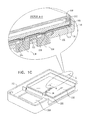
- a secure keypad device 100 including a housing element 102 which, together with a back panel (not shown), defines a keypad device housing.
- Housing element 102 includes, on a top surface 104 thereof, a display aperture 106 , through which a display (not shown) may be viewed, and an array 108 of key apertures 110 .
- a key mat 112 preferably formed of a resilient plastic or rubber, defines a plurality of depressible keys 114 , preferably integrally formed with mat 112 , which partially extend through key apertures 110 .
- a flexible resilient protective partial enclosure 116 which includes an anti-tampering grid 118 , formed of a multiplicity of interconnected anti-tampering electrical conductors, on a top surface 120 thereof and on side surfaces 122 thereof, is provided.
- a flexible cable 124 is coupled to grid 118 .
- Key contact pad 130 Disposed within protective partial enclosure 116 , underlying top surface 120 , is a key contact pad 130 .
- Key contact pad 130 is preferably a resilient, generally planar, pad formed of flexible and resilient plastic or rubber, having an array 132 of raised resilient conductive domes 134 , such as those commercially available from Snaptron, Inc. of Windsor, Colo., USA.
- an electrical circuit board 140 Disposed in predetermined spaced relationship with key contact pad 130 is an electrical circuit board 140 , which functions, inter alia, as a key contact board, defining a plurality of pairs of adjacent electrical contact pads 142 , each pair underlying a corresponding dome 134 , preferably made of carbon, metal or combination of carbon/metal.
- the arrangement of key contact pad 130 and of electrical circuit board 140 is such that depression of a key 114 by the finger of a user causes dome 134 to establish electrical contact with and between a corresponding pair of electrical contact pads 142 lying thereunder and in registration therewith. When key 114 is not depressed, no electrical contact exists between dome 134 and a pair of corresponding electrical contact pads 142 or between the adjacent pads of the pair.
- Electrical circuit board 140 preferably includes an anti-tampering grid 144 formed of a multiplicity of interconnected anti-tampering electrical conductors.
- An electrical connector 146 is arranged for mating connection with flexible cable 124 .
- the anti-tampering grids 118 and 144 are coupled to anti-tampering detection circuitry 148 .
- case-open switches which sense physical tampering and opening of the housing, are provided, preferably within partial enclosure 116 .
- the case-open switches are each embodied in a raised resilient dome 150 , preferably formed of a conductor, mounted on key contact pad 130 .
- the domes may be discrete units or arrays, such as those commercially available from Snaptron, Inc. of Windsor, Colo., USA.
- Domes 150 preferably extend outwardly from the surface of key contact pad 130 to a greater extent than do domes 134 .
- each of domes 150 Disposed on electrical circuit board 140 underlying each of domes 150 are a corresponding number of arrays 152 , each preferably comprising a plurality of mutually concentric conductive pads, such as rings, each array underlying a corresponding dome 150 .
- the arrangement of key contact pad 130 and of electrical circuit board 140 is preferably such that as long as the housing is closed, domes 150 each are in electrical contact with some but not all of the plurality of mutually concentric conductive rings in each of arrays 152 underlying domes 150 and in registration therewith.
- each array 152 comprises an outer ring 153 , an intermediate ring 154 and an inner ring 155 .
- the dome 150 is in electrical contact with outer ring 153 and inner ring 155 but not with intermediate ring 154 .
- Dome 150 is normally in electrical contact with outer ring 153 .
- dome 150 is soldered to outer ring 153 . If tampering is attempted, electrical contact is made between intermediate ring 154 and at least one of dome 150 , outer ring 153 and inner ring 155 .
- each array 152 comprises an outermost ring 156 , a second to outermost ring 157 , an outer intermediate ring 158 , an inner intermediate ring 159 and an inner ring 160 , in this embodiment, as long as the housing is closed and not tampered with, the dome 150 is in electrical contact with outer intermediate ring 158 and inner ring 160 but not with any of outermost ring 156 , second to outermost ring 157 and inner intermediate ring 159 . Dome 150 is normally in electrical contact with outer intermediate ring 158 . Preferably, dome 150 is soldered to outer intermediate ring 158 . If tampering is attempted, electrical contact is made between at least one of outermost ring 156 , second to outermost ring 157 and inner intermediate ring 159 and at least one of dome 150 , outer intermediate ring 158 and inner ring 160 .
- FIGS. 13A and 13B and to FIGS. 14A and 14B are simplified partially sectional and partially schematic illustrations of respective first and second embodiments of the case open switch in respective closed and open operative orientations, coupled to case tamper detection circuitry.
- each dome 150 and corresponding ring 155 is ensured by the provision of a pin 161 , preferably integrally formed on housing element 102 .
- pins 161 urge corresponding protrusions 162 in key mat 112 towards partial enclosure 116 and urge partial enclosure 116 and thus corresponding domes 150 towards ring 155 of array 152 .
- pins 161 urge corresponding protrusions 162 in key mat 112 and thus corresponding domes 150 towards arrays 152 .
- outer ring 153 is grounded, intermediate ring 154 is coupled to a voltage VDD via a resistor R1 and inner ring 155 is coupled to a voltage VDD via a resistor R2.
- a voltage V2 may be measured to indicate whether the housing is open or closed, i.e. whether or not dome 150 is simultaneously in contact with both inner ring 155 and outer ring 153 .
- V2 When this simultaneous contact exists, V2 is zero; otherwise V2 equals VDD.
- An attempt to tamper with the switch by short circuiting inner ring 155 and outer ring 153 will also short circuit intermediate ring 154 and may be detected by measuring a voltage V1.
- V1 is equal to VDD.
- An attempt to tamper with the case open switch causes voltage V1 to be zero.
- pin 161 preferably integrally formed on housing element 102 .
- pins 161 urge corresponding protrusions 162 in key mat 112 towards partial enclosure 116 and urge partial enclosure 116 and thus corresponding domes 150 into electrical contact with rings 160 .
- pins 161 urge corresponding protrusions 162 in key mat 112 and thus corresponding domes 150 towards rings 160 .
- inner ring 160 is coupled to a voltage VCC via a resistor R2
- inner intermediate ring 159 is coupled to voltage VCC via resistor R1
- outer intermediate ring 158 is grounded.
- Outermost ring 156 is grounded and second to outermost ring 157 is coupled to voltage VCC via resistor R1.
- a voltage at tamper detection input points TD2 may be measured to indicate whether the hosing is open or closed, i.e. whether or not dome 150 is simultaneously in contact with both inner ring 160 and outer intermediate ring 158 . When this simultaneous contact exists, voltage measured at TD2 is zero; otherwise voltage measured at TD2 equals VCC. Thus, an attempt to remove of adequate pressure from the dome 150 and open the housing triggers a tamper response.
- An attempt to tamper with the switch for example by applying pressure to the snap dome, such as by drilling a hole in the dome or by injection of conductive glue, results in short circuiting inner ring 160 and outer intermediate ring 158 and inner intermediate ring 159 and may be detected by measuring a voltage at nTD3.
- voltage measured at nTD3 is equal to VCC.
- An attempt to tamper with the case open switch causes voltage measured at nTD3 to be zero.
- rings of array 152 can be of any suitable shape, such as circular or elliptical shape and are preferably concentric.
- peripheral protective grid element 163 which includes an anti-tampering grid 164 , preferably coupled to a flexible cable 165 , which is in turn connected to a connector 166 on electrical circuit board 140 .
- Peripheral protective grid element 163 preferably is located interiorly of the side surfaces 122 of enclosure 116 .
- a bottom protective grid element 168 Fixedly attached to peripheral protective grid element 163 and preferably disposed therebelow is a bottom protective grid element 168 which includes an anti-tampering grid 170 , which is coupled via contacts 172 and via a connector 174 which extends through an aperture 176 formed in peripheral grid element 163 into electrical contact with contacts 178 on electrical circuit board 140 .
- the anti-tampering grids 164 and 170 are coupled to anti tampering detection circuitry 148 .
- FIGS. 2A , 2 B and 2 C illustrate a secure keypad device constructed and operative in accordance with another preferred embodiment of the present invention.
- a secure keypad device 200 including a housing element 202 which, together with a back panel (not shown), defines a keypad device housing.
- Housing element 202 includes, on a top surface 204 thereof, a display aperture 206 , through which a display (not shown) may be viewed, and an array 208 of key apertures 210 .
- a key mat 212 preferably formed of a resilient plastic or rubber, defines a plurality of depressible keys 214 , preferably integrally formed with mat 212 , which partially extend through key apertures 210 .
- a flexible resilient protective partial enclosure 216 which includes an anti-tampering grid 218 , formed of a multiplicity of interconnected anti-tampering electrical conductors, on a top surface 220 thereof and on side surfaces 222 thereof, is provided.
- a flexible cable 224 is coupled to grid 218 .
- Key contact pad 230 Disposed within protective partial enclosure 216 , underlying top surface 220 , is a key contact pad 230 .
- Key contact pad 230 is preferably a resilient, generally planar, pad formed of flexible and resilient plastic or rubber, having an array 232 of raised resilient domes 234 having conductors 236 formed on corresponding bottom facing surfaces 238 thereof.
- a electrical circuit board 240 Disposed in predetermined spaced relationship with key contact pad 230 is a electrical circuit board 240 , which functions, inter alia, as a key contact hoard, defining a plurality of pairs of adjacent electrical contact pads 242 , each pair underlying a corresponding conductor 236 .
- the arrangement of key contact pad 230 and of electrical circuit board 240 is such that depression of a key 214 by the finger of a user causes conductor 236 to establish electrical contact with and between a corresponding pair of electrical contact pads 242 lying thereunder and in registration therewith. When key 214 is not depressed, no electrical contact exists between conductor 236 and a pair of corresponding electrical contact pads 242 or between the adjacent pads of the pair.
- Electrical circuit board 240 preferably includes an anti-tampering grid 244 formed of a multiplicity of interconnected anti-tampering electrical conductors.
- An electrical connector 246 is arranged for mating connection with flexible cable 224 .
- the anti-tampering grids 218 and 214 are coupled to anti-tampering, detection circuitry 248 .
- case-open switches which sense physical tampering and opening of the housing, are also located within partial enclosure 216 .
- the case-open switches are each embodied in a raised resilient dome 250 formed on key contact pad 230 and have conductors 252 formed on an underside surface thereof. Domes 250 preferably extend outwardly from the surface of key contact pad 230 to a greater extent than do domes 234 .
- the case-open switches may be constructed and operative as described hereinabove with reference to one of the embodiments shown FIGS. 1A , 1 B, 13 A- 14 B.
- each of domes 250 Disposed on electrical circuit board 240 underlying each of domes 250 are a corresponding number of pairs of adjacent electrical contact pads 254 , each pair underlying a corresponding conductor 252 .
- the arrangement of key contact pad 230 and of electrical circuit board 240 is such that as long as the housing is closed, conductors 252 each are in electrical contact with and between a corresponding pair of electrical contact pads 254 lying thereunder and in registration therewith. This electrical contact is ensured by the provision of pins 256 integrally formed on housing element 202 .
- pins 256 urge corresponding protrusions 258 in key mat 212 towards partial enclosure 216 and urge partial enclosure 216 and thus corresponding domes 250 and the conductors 252 , on the underside surfaces thereof, into electrical contact with corresponding electrical contact pads 254 .
- peripheral protective grid element 260 which includes an anti-tampering grid 262 , preferably coupled to a flexible cable 264 , which is in turn connected to a connector 266 on electrical circuit board 240 .
- Peripheral protective grid element 260 preferably is located interiorly of the side surfaces 222 of enclosure 216 .
- a bottom protective grid element 268 Fixedly attached to peripheral protective grid element 260 , and preferably disposed therebelow, is a bottom protective grid element 268 which includes an anti-tampering grid 270 , which is coupled via contacts 272 and via a connector 274 , which extends through an aperture 276 formed in peripheral grid element 260 , into electrical contact with contacts 278 on electrical circuit board 240 .
- the anti-tampering grids 262 and 270 are coupled to anti-tampering detection circuitry 248 .
- a structural peripheral enclosure element 280 which is disposed interiorly of the sides 222 of the flexible resilient protective partial enclosure 216 and which provides a peripheral seating surface 282 for electrical circuit board 240 .
- FIG. 3 is a generalized illustration of the electrical connections described hereinabove and includes reference numerals corresponding to both of the above-described embodiments shown respectively in FIGS. 1A-1C and 2 A- 2 C. It may be appreciated from FIG. 3 that all of the anti-tampering grids are connected to the anti-tampering circuitry which is located within the protective enclosure.
- FIGS. 4A and 4B are simplified exploded view illustrations, taken in respective opposite directions, of a secure keypad device constructed and operative in accordance with a further preferred embodiment of the present invention
- FIG. 4C is a simplified illustration the secure keypad device of FIGS. 4A and 4B at various stages of disassembly
- FIG. 5 which is a simplified illustration of electrical connections between anti-tampering elements in the embodiments of FIGS. 4A-4C .
- FIG. 4C is provided to better illustrate the various elements of the keypad device of FIGS. 4A and 4B .
- a secure keypad device 400 including a housing element 402 which, together with a back panel (not shown), defines a keypad device housing.
- Housing element 402 includes, on a top surface 404 thereof, a display aperture 406 , through which a display (not shown) may be viewed, and an array 408 of key apertures 410 .
- An anti-tamper board 412 which includes an anti-tampering grid 414 formed of a multiplicity of interconnected anti-tampering, electrical conductors 416 , underlies top surface 404 and is provided with key apertures 420 in registration with key apertures 410 .
- a peripheral anti-tamper keypad enclosure 422 Fixedly and electrically coupled to anti-tamper board 412 is a peripheral anti-tamper keypad enclosure 422 , which preferably includes an anti-tampering grid 423 formed of a multiplicity of interconnected anti-tampering electrical conductors.
- a key mat 432 preferably formed of a resilient plastic or rubber, defines a plurality of depressible keys 434 , preferably integrally formed with mat 432 , which partially extend through key apertures 410 and 420 and have conductors 436 formed on corresponding bottom facing surfaces 438 thereof.
- An electrical circuit board 440 which functions, inter alia, as a key contact board, is disposed in predetermined spaced relationship with key mat 432 and defines a plurality of pairs of adjacent electrical contact pads 442 , each pair underlying a corresponding conductor 436 .
- the arrangement of key mat 432 and of electrical circuit board 440 is such that depression of a key 434 by the finger of a user causes conductor 436 to establish electrical contact with and between a corresponding pair of electrical contact pads 442 lying thereunder and in registration therewith. When key 434 is not depressed, no electrical contact exists between conductor 436 and a pair of corresponding electrical contact pads 442 or between the adjacent pads of the pair.
- Circuit board 440 preferably includes an anti-tampering grid 444 formed of a multiplicity of interconnected anti-tampering electrical conductors.
- Fixedly coupled to circuit board 440 and an additional electrical circuit board 456 is a peripheral antis tamper enclosure 460 which preferably includes an anti-tampering grid 461 formed of a multiplicity of interconnected anti-tampering electrical conductors.
- Electrical connectors 446 which extend through apertures 443 formed in peripheral anti-tamper enclosure 460 , are coupled via contacts 445 to grid 444 and arranged for mating connection through contacts 457 with an anti-tampering grid 454 , formed of a multiplicity of interconnected anti-tampering, electrical conductors, which is formed on additional electrical circuit board 456 .
- Electrical connectors 471 extend through apertures 473 formed in peripheral anti-tamper keypad enclosure 422 and through apertures 475 formed in circuit board 440 , each underlying corresponding aperture 473 . Electrical connectors 471 are coupled via contacts 477 to anti-tampering grid 461 and arranged for mating connection through contacts 479 with anti-tampering grid 414 .
- Electrical connectors 481 which extend through apertures 483 formed in keymat 432 , are coupled via contacts 485 to anti-tampering grid 414 and arranged for mating connection through contacts 487 with anti-tampering grid 444 .
- Anti-tampering grid 423 is soldered via soldering points 489 on board 422 and soldering points 491 on board 412 to anti-tampering grid 414 .
- anti tampering grids 444 , 414 , 454 , 423 and 461 on boards 440 , 412 and 456 and enclosures 422 and 460 , respectively, are interconnected so as to define an anti-tampering enclosure, which is coupled to and physically encloses anti-tampering detection circuitry 493 .
- anti-tampering grids can be interconnected in numerous ways using various types of connectors.
- case-open switches which sense physical tampering and opening of the housing, are also located within the anti-tampering enclosure.
- the case-open switches are each embodied in conductors 462 mounted on key mat 432 and corresponding pair of electrical contact pads 464 mounted on board 440 .
- the case-open switches may be constructed and operative as described hereinabove with reference to one of the embodiments shown FIGS. 1A , 1 B, 13 A- 14 B.
- pins 465 which extend through apertures 466 in board 412 , force conductors 462 and corresponding pair of electrical contact pads 464 into electrical contact or between the adjacent pads of the pair.
- pins 465 no longer force conductors 462 and corresponding pair of electrical contact pads 464 into electrical contact and as a result electrical contact no longer exists between conductors 462 and corresponding pair of electrical contact pads 464 or between the adjacent pads of the pair and a suitable alarm or disablement occurs.
- FIGS. 6A and 6B are simplified exploded view illustrations, taken in respective opposite directions, of a secure keypad device constructed and operative in accordance with an additional preferred embodiment of the present invention
- FIG. 7 is a simplified illustration of electrical connections between anti-tampering elements in the embodiments of FIGS. 6A and 6B .
- a secure keypad device 600 including a housing element 602 which, together with a back panel (not shown), defines a keypad device housing.
- Housing element 602 includes, on a top surface 604 thereof, a display aperture 606 , through which a display (not shown) may be viewed, and an array 608 of key apertures 610 .
- An anti-tamper board 612 which includes an anti-tampering grid 614 formed of a multiplicity of interconnected anti-tampering electrical conductors 616 , underlies top surface 604 and is provided with key apertures 620 in registration with key apertures 610 .
- a peripheral anti-tamper keypad enclosure 622 Fixedly and electrically coupled to anti-tamper board 612 is a peripheral anti-tamper keypad enclosure 622 , which preferably includes an anti-tampering grid 624 formed of a multiplicity of interconnected anti-tampering electrical conductors.
- a key mat 632 preferably formed of a resilient plastic or rubber, defines a plurality of depressible keys 634 which partially extend through key apertures 610 and 620 .
- a flexible resilient protective element 636 preferably a resilient generally planar pad formed of flexible and resilient plastic or rubber which includes an anti-tampering grid 638 formed of a multiplicity of interconnected anti-tampering electrical conductors, is provided.
- An electrical cable 640 is coupled to grid 638 .
- a key contact pad 642 Disposed below element 636 is a key contact pad 642 , preferably a resilient generally planar pad formed of flexible and resilient plastic or rubber, having an array 644 of raised resilient domes 646 having conductors 648 formed on corresponding bottom facing surfaces 650 thereof.
- An electrical circuit board 660 is disposed in predetermined spaced relationship with key mat 632 and defines a plurality of pairs of adjacent electrical contact pads 662 , each pair underlying a corresponding conductor 648 .
- the arrangement of key mat 632 and of electrical circuit board 660 is such that depression of a key 634 by the finger of a user causes conductor 648 to establish electrical contact with and between a corresponding pair of electrical contact pads 662 lying thereunder and in registration therewith. When key 634 is not depressed, no electrical contact exists between conductor 648 and a pair of corresponding pads 662 or between the adjacent pads of the pair.
- Circuit board 660 preferably includes an anti-tampering grid 664 , formed of a multiplicity of interconnected anti-tampering electrical conductors.
- a peripheral anti-tamper enclosure 672 Fixedly and electrically coupled to board 660 and to an additional electrical circuit board 670 is a peripheral anti-tamper enclosure 672 , which preferably includes an anti-tampering grid 676 formed of a multiplicity of interconnected anti-tampering electrical conductors.
- Electrical connectors 666 which extend through apertures 667 in peripheral anti-tamper enclosure 672 , are coupled via contacts 665 to grid 664 and arranged for mating connection through contacts 669 with an anti-tampering grid 668 formed of a multiplicity of interconnected anti-tampering electrical conductors on additional electrical circuit board 670 .
- Electrical connectors 677 extend through apertures 679 formed in peripheral anti-tamper keypad enclosure 622 and through apertures 681 formed in board 660 , each underlying corresponding aperture 679 . Electrical connectors 677 are coupled via contacts 673 to anti-tampering grid 676 and arranged for mating connection through contacts 675 with anti-tampering grid 614 .
- Flexible electrical cable 640 is connected to a connector 683 on electrical circuit board 660 .
- Electrical connectors 691 extend through apertures 693 formed in flexible element 636 and through apertures 695 formed in key contact pad 642 and corresponding apertures 696 formed in key mat 632 . Electrical connectors 691 are coupled via contacts 697 to anti-tampering grid 664 and arranged for mating connection through contacts 699 with an anti-tampering grid 614 .
- Anti-tampering grid 624 is soldered to anti-tampering grid 614 .
- anti tampering grids 614 , 664 , 668 , 638 , 624 and 676 , on boards 612 , 660 and 670 , element 636 and enclosures 622 and 672 , respectively, are interconnected so as to define an anti-tampering enclosure, which is coupled to and physically encloses anti-tampering detection circuitry 674 .
- case-open switches which sense physical tampering and opening of the housing, are also located within the anti-tampering enclosure.
- the case-open switches are each embodied in conductors 680 mounted on the bottom facing of domes 641 of key contact pad 642 and corresponding pairs of electrical contact pads 682 mounted on board 660 .
- the case-open switches may be constructed and operative as described hereinabove with reference to one of the embodiments shown FIGS. 1A , 1 B, 13 A- 14 B.
- pins 684 which extend through apertures 686 in board 612 , urge corresponding protrusions 631 on key mat 632 towards element 636 and key contact pad 642 and urge domes 641 on key contact pad 642 towards board 660 and thus force conductors 680 and pair of electrical contact pads 682 into electrical contact.
- pins 684 no longer force conductors 680 and pair of electrical contact pads 682 into electrical contact and as a result electrical contact no longer exists between conductors 680 and pair of electrical contact pads 682 and a suitable alarm or disablement occurs.
- FIG. 8 is a simplified exploded view illustration of a secure keypad device constructed and operative in accordance with a still further preferred embodiment of the present invention
- FIGS. 9A & 9B are simplified sectional illustrations of part of the device of FIG. 8 , taken along lines IX-IX in FIG. 8 , in respective key non-depressed and key depressed operative orientations.
- a secure keypad device 800 including a housing element 802 which, together with a back panel (not shown), defines a keypad device housing.
- Housing element 802 includes, on a top surface 804 thereof, a display aperture 806 , through which a display (not shown) may be viewed, and an array 808 of key apertures 810 .
- An anti-tamper board 812 which includes an anti-tampering grid 814 formed of a multiplicity of interconnected anti-tampering electrical conductors, underlies top surface 804 and is provided with key apertures 820 in registration with key apertures 810 .
- Fixedly and electrically coupled to anti-tamper hoard 812 is a peripheral anti-tamper keypad enclosure 822 , which preferably includes an anti-tampering grid 824 formed of a multiplicity of interconnected anti-tampering electrical conductors.
- a key mat 832 preferably formed of a resilient plastic or rubber, defines a plurality of depressible keys 834 which partially extend through key apertures 810 and 820 .
- Conductors 836 are formed on key mat 832 .
- Pairs of adjacent electrical contact pads 838 are located on board 812 in registration with conductors 836 and are arranged such that when keys 834 are in a non-depressed operative orientation, such as that shown in FIG. 9A , electrical contact exists between conductors 836 and pairs of adjacent electrical contact pads 838 lying thereover and in registration therewith and between those pairs of adjacent electrical contact pads 838 .
- keys 834 are in a depressed operative orientation, such as that shown in FIG. 9B , no electrical contact exists between conductors 836 and pairs of adjacent electrical contact pads 838 lying thereover and in registration therewith and between those pairs of adjacent electrical contact pads 838 .
- An electrical circuit board 840 is disposed in predetermined spaced relationship with key mat 832 .
- Board 840 preferably includes an anti-tampering grid 844 formed of a multiplicity of interconnected anti-tampering electrical conductors.
- Electrical connectors 846 are coupled to grid 844 and arranged for mating connection with an anti-tampering grid 854 , formed of a multiplicity of interconnected anti-tampering electrical conductors, which is formed on an additional electrical circuit board 856 .
- Fixedly and electrically coupled to boards 840 and 856 is a peripheral anti-tamper enclosure 858 which preferably includes an anti-tampering grid 859 , formed of a multiplicity of interconnected anti-tampering electrical conductors.
- anti tampering grids 844 , 854 and 859 , on boards 840 and 856 and peripheral anti-tamper enclosure 858 , respectively, are interconnected so as to define an anti-tampering enclosure, which is coupled to and physically encloses anti-tampering detection circuitry (not shown). It is also appreciated that anti tampering grids 814 and 824 on board 812 and enclosure 822 are coupled to anti-tampering circuitry (not shown) and preferably interconnected to anti tampering grids 844 , 854 and 859 on boards 840 and 856 and enclosure 858 .
- case-open switches which sense physical tampering and opening of the housing, are also located within the anti-tampering enclosure.
- the case-open switches are each embodied in conductors (not shown) mounted on key mat 832 and formed on underside surface thereof, and corresponding pair of electrical pads 864 mounted on board 840 .
- the case-open switches may be constructed and operative as described hereinabove with reference to one of the embodiments shown FIGS. 1A , 1 B, 13 A- 14 B.
- pins (not shown) extend through apertures (not shown) in board 812 and force pair of electrical contacts 864 and corresponding conductors (not shown) on key mat 832 into electrical contact.
- pins 864 no longer force conductors on key mat 832 and pair of electrical pads 864 into electrical contact and as a result electrical contact no longer exists between conductors on key mat 832 and pair of electrical contacts 864 and a suitable alarm or disablement occurs.
- FIG. 10 is a simplified exploded view illustration of a secure keypad device constructed and operative in accordance with a yet further preferred embodiment of the present invention
- FIGS. 11A & 11B are simplified sectional illustrations of part of the device of FIG. 10 , taken along lines XI-XI in FIG. 10 , in respective key non-depressed and key depressed operative orientations.
- a secure keypad device 900 including a housing element 902 which, together with a back panel (not shown), defines a keypad device housing.
- Housing element 902 includes a display aperture 906 , through which a display (not shown) may be viewed, and an array 908 of key apertures 910 .
- An anti-tamper board 912 which includes an anti-tampering grid 914 formed of a multiplicity of interconnected anti-tampering electrical conductors, underlies top surface of housing element 902 and is provided with key apertures 920 in registration with key apertures 910 .
- a peripheral anti-tamper keypad enclosure 922 Fixedly and electrically coupled to anti-tamper board 912 is a peripheral anti-tamper keypad enclosure 922 , which preferably includes an anti-tampering grid 923 , formed of a multiplicity of interconnected anti-tampering electrical conductors.
- a key mat 932 preferably formed of a resilient plastic or rubber, defines a plurality of depressible keys 934 which partially extend through key apertures 910 and 920 .
- Conductors 936 are formed on an underside surface 938 of key mat 932 , preferably on opposite sides of each of keys 934 .
- An electrical circuit board 940 which functions, inter alia, as a key contact board, is disposed in predetermined spaced relationship with key mat 932 and defines a plurality of pairs of adjacent electrical contact pads 942 , each pair underlying a corresponding conductor 936 .
- keys 934 When keys 934 are in a non-depressed operative orientation, such as that shown in FIG. 11A , electrical contact does not exist between conductors 936 and pairs of adjacent electrical contact pads 942 lying thereunder and in registration therewith and between those pairs of adjacent electrical contact pads 942 .
- keys 934 When keys 934 are in a depressed operative orientation, such as that shown in FIG. 11B , electrical contact exists between conductors 936 and pairs of adjacent electrical contact pads 942 lying thereunder in registration therewith and between those pairs of adjacent electrical contact pads 942 .
- Board 940 preferably includes an anti-tampering grid 944 , formed of a multiplicity of interconnected anti-tampering electrical conductors. Electrical connectors 946 are coupled to grid 944 and arranged for mating connection with an anti-tampering grid 954 , formed of a multiplicity of interconnected anti-tampering electrical conductors, which is formed on an additional electrical circuit board 956 . Fixedly and electrically coupled to boards 940 and 956 is a peripheral anti-tamper enclosure 958 which preferably includes an anti-tampering grid 957 formed of a multiplicity of interconnected anti-tampering electrical conductors.
- anti tampering grids 944 , 954 and 957 on boards 940 and 956 and peripheral anti-tamper enclosure 958 , respectively, are interconnected so as to define an anti-tampering enclosure, which is coupled to and physically encloses anti-tampering detection circuitry 959 .
- Electrical connectors 980 and 982 preferably couple grids 914 and 923 on board 912 and enclosure 922 , respectively, to anti-tampering detection circuitry 959 .
- case-open switches which sense physical tampering and opening of the housing are also located within the anti-tampering enclosure.
- the case-open switches are each embodied in conductors 962 mounted on key mat 932 and corresponding conductors (not shown) mounted on board 940 .
- the case-open switches may be constructed and operative as described hereinabove with reference to one of the embodiments shown FIGS. 1A , 1 B, 13 A- 14 B.
- pins 966 When the housing is closed, pins 966 extend through apertures 968 in board 912 and force conductors 962 into electrical contact with the corresponding conductors on board 940 . When the housing is opened, pins 966 no longer force conductors 962 into electrical contact with the corresponding conductors on board 940 and as a result electrical contact no longer exists between conductors 962 and the corresponding conductors on board 940 and a suitable alarm or disablement occurs.
- FIGS. 12A and 12B are simplified exploded view illustrations, taken in respective opposite directions, of a secure keypad device constructed and operative in accordance with still another preferred embodiment of the present invention.
- a secure keypad device 1100 including a housing element 1102 which, together with a hack panel (not shown), defines a keypad device housing.
- Housing element 1102 includes, on a top surface 1104 thereof; a display aperture 1106 , through which a display (not shown) may be viewed, and an array 1108 of depressible keys 1110 , preferably integrally formed with housing element 1102 .
- Keys 1110 are preferably formed of a resilient plastic or rubber and partially extend above top surface 1104 of housing element 1102 . As seen particularly in section A-A enlargement in FIG. 12A , a contact surface 1112 of each of keys 1110 extends below top surface 1104 of housing element 1102 . Keys 1110 preferably include an attachment portion 1113 and a connection portion 1114 .
- a flexible resilient protective partial enclosure 1116 which includes an anti-tampering grid 1118 , formed of a multiplicity of interconnected anti-tampering electrical conductors, on a top surface 1120 thereof and on side surfaces 1122 thereof, is provided.
- a flexible cable 1124 is coupled to grid 1118 .
- Key contact pad 1130 Disposed within protective partial enclosure 1116 , underlying top surface 1120 , is a key contact pad 1130 .
- Key contact pad 1130 is preferably a resilient, generally planar, pad formed of flexible and resilient plastic or rubber, having an array 1132 of raised resilient domes 1134 with conductors 1136 being formed on corresponding bottom facing surfaces 1138 thereof.
- an electrical circuit board 1140 Disposed in predetermined spaced relationship with key contact pad 1130 is an electrical circuit board 1140 , which functions, inter alia, as a key contact board, defining a plurality of pairs of adjacent electrical contact pads 1142 , each pair underlying a corresponding conductor 1136 , preferably made of carbon, metal or combination of carbon/metal.
- the arrangement of key contact pad 1130 and of electrical circuit board 1140 is such that depression of a key 1110 by the finger of a user causes conductor 1136 to establish electrical contact with and between a corresponding pair of electrical contact pads 1142 lying thereunder and in registration therewith. When key 1110 is not depressed, no electrical contact exists between conductor 1136 and a pair of corresponding electrical contact pads 1142 or between the adjacent pads of the pair.
- Electrical circuit hoard 1140 preferably includes an anti-tampering grid 1144 formed of a multiplicity of interconnected anti-tampering electrical conductors.
- An electrical connector 1146 is arranged for mating connection with flexible cable 1124 .
- the anti-tampering grids 1118 and 1144 are coupled to anti-tampering detection circuitry 1148 .
- case-open switches which sense physical tampering and opening of the housing, are also located within partial enclosure 1116 .
- the case-open switches are each embodied in a raised resilient dome 1150 formed on key contact pad 1130 and have conductors 1152 formed on an underside surface thereof. Domes 1150 preferably extend outwardly from the surface of key contact pad 1130 to a greater extent than do domes 1134 .
- the case-open switches may be constructed and operative as described hereinabove with reference to one of the embodiments shown FIGS. 1A , 1 B, 13 A- 14 B.
- each of domes 1150 Disposed on electrical circuit board 1140 underlying each of domes 1150 are a corresponding number of pairs of adjacent electrical contact pads 1154 , each pair underlying a corresponding conductor 1152 .
- the arrangement of key contact pad 1130 and of electrical circuit board 1140 is such that as long as the housing is closed, conductors 1152 each are in electrical contact with and between a corresponding pair of electrical contact pads 1154 lying thereunder and in registration therewith. This electrical contact is ensured by the provision of pins 1156 integrally formed on housing element 1102 . When the housing is closed, pins 1156 urge element 1116 and thus corresponding domes 1150 on contact pad 1130 , and thus corresponding conductors 1152 , on the underside surfaces thereof, into electrical contact with corresponding electrical contact pads 1154 .
- a peripheral protective grid element 1160 which includes an anti-tampering grid 1162 , preferably coupled to a flexible cable 1164 , which is in turn connected to a connector 1166 on electrical circuit board 1140 .
- Peripheral protective grid element 1160 preferably is located interiorly of the side surfaces 1122 of enclosure 1116 .
- a bottom protective grid element 1168 Fixedly attached to peripheral protective grid element 1160 and preferably disposed therebelow is a bottom protective grid element 1168 which includes an anti-tampering grid 1170 , which is coupled via contacts 1172 and via a connector 1174 which extends through an aperture 1176 formed in peripheral grid element 1160 into electrical contact with contacts 1178 on electrical circuit board 1140 .
- the anti-tampering grids 1162 and 1170 are coupled to anti-tampering detection circuitry 1148 .
Landscapes
- Engineering & Computer Science (AREA)
- Theoretical Computer Science (AREA)
- Computer Hardware Design (AREA)
- General Engineering & Computer Science (AREA)
- Physics & Mathematics (AREA)
- General Physics & Mathematics (AREA)
- Human Computer Interaction (AREA)
- Computer Security & Cryptography (AREA)
- Software Systems (AREA)
- Push-Button Switches (AREA)
Abstract
Description
- U.S. Published Patent Application No. 2008/0278353;
- U.S. Pat. Nos. 7,270,275; 6,646,565; 6,917,299 and 4,486,637;
- European Patent Nos.: 1421549 and 1676182; and
- Great Britain Patent Application No. GB8608277.
Claims (15)
Priority Applications (1)
| Application Number | Priority Date | Filing Date | Title |
|---|---|---|---|
| US14/592,296 US9250709B2 (en) | 2008-01-22 | 2015-01-08 | Secure point of sale terminal |
Applications Claiming Priority (6)
| Application Number | Priority Date | Filing Date | Title |
|---|---|---|---|
| US1199308P | 2008-01-22 | 2008-01-22 | |
| US12/355,857 US9013336B2 (en) | 2008-01-22 | 2009-01-19 | Secured keypad devices |
| PCT/IL2009/000724 WO2010082190A1 (en) | 2009-01-19 | 2009-07-23 | Secure point of sale terminal |
| US66605411A | 2011-08-01 | 2011-08-01 | |
| US14/082,704 US9032222B2 (en) | 2008-01-22 | 2013-11-18 | Secure point of sale terminal |
| US14/592,296 US9250709B2 (en) | 2008-01-22 | 2015-01-08 | Secure point of sale terminal |
Related Parent Applications (1)
| Application Number | Title | Priority Date | Filing Date |
|---|---|---|---|
| US14/082,704 Continuation US9032222B2 (en) | 2008-01-22 | 2013-11-18 | Secure point of sale terminal |
Publications (2)
| Publication Number | Publication Date |
|---|---|
| US20150128297A1 US20150128297A1 (en) | 2015-05-07 |
| US9250709B2 true US9250709B2 (en) | 2016-02-02 |
Family
ID=42340568
Family Applications (4)
| Application Number | Title | Priority Date | Filing Date |
|---|---|---|---|
| US12/355,857 Active 2033-02-19 US9013336B2 (en) | 2008-01-22 | 2009-01-19 | Secured keypad devices |
| US14/592,296 Active US9250709B2 (en) | 2008-01-22 | 2015-01-08 | Secure point of sale terminal |
| US14/658,847 Active US9436293B2 (en) | 2008-01-22 | 2015-03-16 | Secured keypad devices |
| US15/225,086 Active US9779270B2 (en) | 2008-01-22 | 2016-08-01 | Secured keypad devices |
Family Applications Before (1)
| Application Number | Title | Priority Date | Filing Date |
|---|---|---|---|
| US12/355,857 Active 2033-02-19 US9013336B2 (en) | 2008-01-22 | 2009-01-19 | Secured keypad devices |
Family Applications After (2)
| Application Number | Title | Priority Date | Filing Date |
|---|---|---|---|
| US14/658,847 Active US9436293B2 (en) | 2008-01-22 | 2015-03-16 | Secured keypad devices |
| US15/225,086 Active US9779270B2 (en) | 2008-01-22 | 2016-08-01 | Secured keypad devices |
Country Status (2)
| Country | Link |
|---|---|
| US (4) | US9013336B2 (en) |
| WO (1) | WO2010082190A1 (en) |
Families Citing this family (32)
| Publication number | Priority date | Publication date | Assignee | Title |
|---|---|---|---|---|
| US9013336B2 (en) | 2008-01-22 | 2015-04-21 | Verifone, Inc. | Secured keypad devices |
| US8595514B2 (en) | 2008-01-22 | 2013-11-26 | Verifone, Inc. | Secure point of sale terminal |
| US8432300B2 (en) * | 2009-03-26 | 2013-04-30 | Hypercom Corporation | Keypad membrane security |
| WO2010142748A1 (en) * | 2009-06-09 | 2010-12-16 | Gilbarco, S.R.L. | Fuel dispenser user interface |
| CN101697182B (en) * | 2009-09-29 | 2011-10-05 | 广州广电运通金融电子股份有限公司 | Encryption keyboard |
| US8358218B2 (en) | 2010-03-02 | 2013-01-22 | Verifone, Inc. | Point of sale terminal having enhanced security |
| US8330606B2 (en) | 2010-04-12 | 2012-12-11 | Verifone, Inc. | Secure data entry device |
| US8405506B2 (en) | 2010-08-02 | 2013-03-26 | Verifone, Inc. | Secure data entry device |
| CN101937589B (en) * | 2010-08-20 | 2012-10-03 | 广州广电运通金融电子股份有限公司 | Anti-prying encryption keyboard |
| US8593824B2 (en) | 2010-10-27 | 2013-11-26 | Verifone, Inc. | Tamper secure circuitry especially for point of sale terminal |
| US9053376B2 (en) * | 2010-12-07 | 2015-06-09 | Compagnie Industrielle et Financiere D'Ingenierie “Ingenico” | Electronic payment device |
| CN102402252A (en) * | 2011-11-23 | 2012-04-04 | 苏州佳世达电通有限公司 | Electronic device |
| CN103367003B (en) * | 2012-04-11 | 2015-04-22 | 深圳市证通电子股份有限公司 | Encrypted keyboard and button scanning protective device |
| US9691066B2 (en) | 2012-07-03 | 2017-06-27 | Verifone, Inc. | Location-based payment system and method |
| GB201223471D0 (en) * | 2012-12-28 | 2013-02-13 | Johnson Electric Sa | Electronic device with tamper resistant enclosure |
| US9430675B2 (en) | 2013-05-21 | 2016-08-30 | Ncr Corporation | Encrypting pin pad |
| US20150008111A1 (en) * | 2013-07-02 | 2015-01-08 | Verifone, Inc. | Keypad |
| GB2518860B (en) * | 2013-10-02 | 2016-05-04 | Powa Tech Ltd | Secure data entry device |
| US9213869B2 (en) | 2013-10-04 | 2015-12-15 | Verifone, Inc. | Magnetic stripe reading device |
| US20160026275A1 (en) | 2014-07-23 | 2016-01-28 | Verifone, Inc. | Data device including ofn functionality |
| GB2529622A (en) * | 2014-08-22 | 2016-03-02 | Johnson Electric Sa | Improvements in or relating to an anti-tamper device |
| US9904815B2 (en) | 2014-09-16 | 2018-02-27 | Verifone, Inc. | Secure smartcard reader |
| US9817482B2 (en) | 2014-11-17 | 2017-11-14 | Verifone, Inc. | Secure keypad including conductive trace |
| US9595174B2 (en) | 2015-04-21 | 2017-03-14 | Verifone, Inc. | Point of sale terminal having enhanced security |
| WO2017155128A1 (en) * | 2016-03-07 | 2017-09-14 | 주식회사 블루버드 | Mobile terminal having security function |
| TWI598766B (en) * | 2016-03-14 | 2017-09-11 | 神雲科技股份有限公司 | An anti-tamper system and an anti-tamper circuit |
| FR3061972B1 (en) * | 2017-01-13 | 2020-02-14 | Ingenico Group | SECURE MEMORY CARD READER BODY |
| US10306753B1 (en) | 2018-02-22 | 2019-05-28 | International Business Machines Corporation | Enclosure-to-board interface with tamper-detect circuit(s) |
| US11122682B2 (en) | 2018-04-04 | 2021-09-14 | International Business Machines Corporation | Tamper-respondent sensors with liquid crystal polymer layers |
| US10984141B2 (en) | 2018-10-26 | 2021-04-20 | Hamilton Sundstrand Corporation | Self-powering tamper detection and response system architecture |
| US10544923B1 (en) | 2018-11-06 | 2020-01-28 | Verifone, Inc. | Devices and methods for optical-based tamper detection using variable light characteristics |
| US11709972B2 (en) * | 2020-02-21 | 2023-07-25 | Te Connectivity Solutions Gmbh | Substrate for a tamper sensor |
Citations (80)
| Publication number | Priority date | Publication date | Assignee | Title |
|---|---|---|---|---|
| GB892198A (en) | 1960-06-07 | 1962-03-21 | American District Telegraph Co | Electrical protection system |
| US3466643A (en) | 1966-03-18 | 1969-09-09 | Carlton Swain Moorefield | Transmission line tampering alarm system |
| DE2241738A1 (en) | 1971-09-22 | 1973-03-29 | Securiton Ag | SHOULDER DISTRIBUTORS FOR ALARM SYSTEMS |
| US3735353A (en) | 1971-10-28 | 1973-05-22 | Johnson Service Co | Alarm transmission line security system utilizing pseudo random encoding |
| US3941964A (en) | 1974-12-09 | 1976-03-02 | Bowmar Instrument Corporation | Push-button type binary switch device |
| US4486637A (en) | 1982-06-28 | 1984-12-04 | Northern Telecom Limited | Pushbutton switch assembly |
| US4527030A (en) | 1980-11-06 | 1985-07-02 | Preh Elektrofeinmechanische Werke, Jakob Preh Nachf., Gmbh & Co. | Keyboard |
| US4593384A (en) | 1984-12-21 | 1986-06-03 | Ncr Corporation | Security device for the secure storage of sensitive data |
| GB2178235A (en) | 1985-04-04 | 1987-02-04 | British Telecomm | Keypad |
| US4749368A (en) | 1986-04-03 | 1988-06-07 | E. I. Du Pont De Nemours And Company | Contact strip terminal |
| US4807284A (en) | 1986-09-24 | 1989-02-21 | Ncr Corporation | Security device for sensitive data |
| US4847595A (en) | 1986-12-08 | 1989-07-11 | Atsumi Denki Kabushiki Kaisha | Alarm system |
| EP0375545A1 (en) | 1988-12-20 | 1990-06-27 | Bull S.A. | Device to protect an electronic card and its use to protect a reading terminal of a magnetic and/or microprocessor card |
| US5086292A (en) | 1989-10-31 | 1992-02-04 | Iris Systems Inc. | Tamper detection device for utility meter |
| US5237307A (en) | 1991-11-27 | 1993-08-17 | The United States Of America As Represented By The United States Department Of Energy | Non-contact tamper sensing by electronic means |
| US5239664A (en) | 1988-12-20 | 1993-08-24 | Bull S.A. | Arrangement for protecting an electronic card and its use for protecting a terminal for reading magnetic and/or microprocessor cards |
| US5353350A (en) | 1989-10-03 | 1994-10-04 | University Of Technology | Electro-active cradle circuits for the detection of access or penetration |
| US5506566A (en) | 1993-05-06 | 1996-04-09 | Northern Telecom Limited | Tamper detectable electronic security package |
| US5559311A (en) | 1994-12-27 | 1996-09-24 | General Motors Corporation | Dual detent dome switch assembly |
| US5586042A (en) | 1993-03-15 | 1996-12-17 | Hughey-Pisau, Ltd. | Apparatus and methods for measuring and detecting variations in the value of a capacitor |
| US5675319A (en) | 1996-04-26 | 1997-10-07 | David Sarnoff Research Center, Inc. | Tamper detection device |
| US5809143A (en) | 1995-12-12 | 1998-09-15 | Hughes; Thomas S. | Secure keyboard |
| US5861662A (en) | 1997-02-24 | 1999-01-19 | General Instrument Corporation | Anti-tamper bond wire shield for an integrated circuit |
| US5877547A (en) | 1994-11-17 | 1999-03-02 | Schlumberger Industries | Active security device including an electronic memory |
| US5998858A (en) | 1995-07-20 | 1999-12-07 | Dallas Semiconductor Corporation | Microcircuit with memory that is protected by both hardware and software |
| WO2001063994A2 (en) | 2000-02-23 | 2001-08-30 | Iridian Technologies, Inc. | Tamper proof case for electronic devices having memories with sensitive information |
| US6288640B1 (en) | 1995-12-15 | 2001-09-11 | GAGNON ANDRé | Open transmission line intrusion detection system using frequency spectrum analysis |
| FR2806507A1 (en) | 2000-03-17 | 2001-09-21 | Dassault Automatismes | ANTI-INTRUSION ELASTOMERIC MEMBRANE FOR SECURE ELECTRONIC UNITS |
| US20010032211A1 (en) | 2000-04-13 | 2001-10-18 | Hiroshi Kuzumaki | Question answering system and storage medium |
| US6359338B1 (en) | 1999-07-09 | 2002-03-19 | Oki Electric Industry Co., Ltd. | Semiconductor apparatus with self-security function |
| JP2002108711A (en) | 2000-09-29 | 2002-04-12 | Tamura Electric Works Ltd | Data processor and data processing method |
| US6396400B1 (en) | 1999-07-26 | 2002-05-28 | Epstein, Iii Edwin A. | Security system and enclosure to protect data contained therein |
| US6414884B1 (en) | 2000-02-04 | 2002-07-02 | Lucent Technologies Inc. | Method and apparatus for securing electronic circuits |
| GB2372363A (en) | 2000-12-01 | 2002-08-21 | Peter Gwynne | Security device having a capacitive sensor |
| US6438825B1 (en) | 1995-03-28 | 2002-08-27 | Intel Corporation | Method to prevent intrusions into electronic circuitry |
| US6463263B1 (en) | 1999-02-01 | 2002-10-08 | Telefonaktiebolaget Lm Ericsson (Publ) | Communication station |
| US6466118B1 (en) | 2002-04-17 | 2002-10-15 | Duraswitch Industries, Inc. | Overlay electrical conductor for a magnetically coupled pushbutton switch |
| WO2003019467A1 (en) | 2001-08-31 | 2003-03-06 | Trintech Limited | A pin pad |
| JP2003100169A (en) | 2001-09-21 | 2003-04-04 | Fuji Denshi Kogyo Kk | Dome contact sheet and switch with click action |
| US6563488B1 (en) | 1997-09-29 | 2003-05-13 | Varatouch Technology Incorporated | Pointing device with integrated switch |
| US6571948B2 (en) | 2001-06-28 | 2003-06-03 | Bellsouth Intellectual Property Corporation | Keyboard lock box |
| US6633241B2 (en) | 1999-12-28 | 2003-10-14 | Nokia Mobile Phones Ltd. | Capacitively coupled keypad structure |
| US6646565B1 (en) | 2000-06-01 | 2003-11-11 | Hewlett-Packard Development Company, L.P. | Point of sale (POS) terminal security system |
| US6669100B1 (en) | 2002-06-28 | 2003-12-30 | Ncr Corporation | Serviceable tamper resistant PIN entry apparatus |
| US20040031673A1 (en) | 2002-05-23 | 2004-02-19 | Levy David H. | Keypads and key switches |
| EP1432031A1 (en) | 2002-12-20 | 2004-06-23 | Lipman Electronic Engineering Ltd. | Anti-tampering enclosure for electronic circuitry |
| US20040118670A1 (en) | 2002-12-03 | 2004-06-24 | Sung-Sun Park | Rotation key device for a portable terminal |
| US6830182B2 (en) | 2002-04-11 | 2004-12-14 | Cis Eletronica Industria E Comercio Ltda. | Magnetic card reader |
| US6874092B1 (en) | 1998-10-06 | 2005-03-29 | Ricoh Corporation | Method and apparatus for erasing data after tampering |
| WO2005041002A1 (en) | 2003-10-24 | 2005-05-06 | Verifone Systems Ireland Limited | Circuit security |
| US20050138433A1 (en) | 2003-12-23 | 2005-06-23 | Zone Labs, Inc. | Security System with Methodology for Defending Against Security Breaches of Peripheral Devices |
| US6912280B2 (en) | 2002-07-22 | 2005-06-28 | Sony Ericsson Mobile Communications Ab | Keypad device |
| US20050184870A1 (en) | 2004-02-25 | 2005-08-25 | Dmatek, Ltd. | Method and apparatus for portable transmitting devices |
| US6936777B1 (en) | 2004-03-12 | 2005-08-30 | Fuji Electronics Industries Co., Ltd. | Two-step switch |
| GB2411756A (en) | 2004-03-04 | 2005-09-07 | Dione Plc | Secure card reader |
| WO2005086546A2 (en) | 2004-03-04 | 2005-09-15 | Lipman Electronics Engineering Limited | Secure card reader |
| US20070016963A1 (en) | 2005-07-14 | 2007-01-18 | Xac Automation Corp. | PIN entry terminal having security system |
| US20070040674A1 (en) | 2005-08-16 | 2007-02-22 | Honeywell International, Inc. | Conductive tamper switch for security devices |
| US20070196156A1 (en) | 2006-02-22 | 2007-08-23 | Lewis Jeremiah J | Computer Keyboard and Mouse Security Shield |
| US20070204173A1 (en) | 2006-02-15 | 2007-08-30 | Wrg Services Inc. | Central processing unit and encrypted pin pad for automated teller machines |
| US7270275B1 (en) | 2004-09-02 | 2007-09-18 | Ncr Corporation | Secured pin entry device |
| US7283066B2 (en) | 1999-09-15 | 2007-10-16 | Michael Shipman | Illuminated keyboard |
| FR2911000A1 (en) | 2006-12-29 | 2008-07-04 | Nicomatic Sa Sa | Metallic contact dome for switch in motor vehicle, has contact zone whose projecting distance is such that contact zone reaches tangential plane before central projection during handling of dome by applying force towards tangential plane |
| US20080180245A1 (en) | 2007-01-25 | 2008-07-31 | Verifone, Inc. | Anti-tamper protected enclosure |
| US20080278353A1 (en) | 2007-05-11 | 2008-11-13 | Measurement Specialties, Inc. | Tamper resistant electronic transaction assembly |
| US7497378B2 (en) | 2006-12-08 | 2009-03-03 | Verifone, Inc. | Anti-tampering protection for magnetic stripe reader |
| US20090058628A1 (en) | 2007-08-27 | 2009-03-05 | Verifone, Inc. | Secure point of sale device employing capacitive sensors |
| WO2009091394A1 (en) | 2008-01-16 | 2009-07-23 | Snaptron Inc. | Tactile apparatus and methods |
| WO2010082190A1 (en) | 2009-01-19 | 2010-07-22 | Verifone, Inc. | Secure point of sale terminal |
| US7784691B2 (en) | 2006-12-08 | 2010-08-31 | Verifone Inc. | Security functionality for magnetic card readers and point of sales devices |
| US7835521B1 (en) | 2005-12-02 | 2010-11-16 | Google Inc. | Secure keyboard |
| US20110063109A1 (en) | 2007-11-29 | 2011-03-17 | Hypercom Gmbh | Device for monitoring a space by series-connected normally-open contacts, in particular cover interlock switches in a security enclosure |
| US20110215938A1 (en) | 2010-03-02 | 2011-09-08 | Verifone, Inc. | Point of sale terminal having enhanced security |
| US20110248860A1 (en) | 2010-04-12 | 2011-10-13 | Amihay Avital | Secure data entry device |
| US20110279279A1 (en) | 2008-01-22 | 2011-11-17 | Verifone, Inc. | Secure point of sale terminal |
| US20120025983A1 (en) | 2010-08-02 | 2012-02-02 | Verifone, Inc. | Secure data entry device |
| US20120106113A1 (en) | 2010-10-27 | 2012-05-03 | Verifone, Inc. | Tamper secure circuitry especially for point of sale terminal |
| US20120180140A1 (en) | 2011-01-06 | 2012-07-12 | Verifone, Inc. | Secure pin entry device |
| US20130067534A1 (en) | 2010-05-20 | 2013-03-14 | High Sec Labs Ltd. | Computer motherboard having peripheral security functions |
| US8513548B2 (en) | 2010-07-21 | 2013-08-20 | Maxim Integrated Products, Inc. | Keypad having tamper-resistant keys |
Family Cites Families (25)
| Publication number | Priority date | Publication date | Assignee | Title |
|---|---|---|---|---|
| US4275378A (en) | 1978-05-23 | 1981-06-23 | Kiloking (Proprietary) Limited | Monitoring the operation of a vehicle |
| US5426360A (en) | 1994-02-17 | 1995-06-20 | Niagara Mohawk Power Corporation | Secondary electrical power line parameter monitoring apparatus and system |
| US6117539A (en) | 1996-10-28 | 2000-09-12 | Thomas & Betts Inernational, Inc. | Conductive elastomer for grafting to an elastic substrate |
| US6087939A (en) | 1998-09-22 | 2000-07-11 | Se-Kure Controls, Inc. | Security system |
| US7351919B1 (en) | 1999-07-15 | 2008-04-01 | Thomson Licensing | Port cover for limiting transfer of electromagnetic radiation from a port defined in a host device |
| US6970068B1 (en) | 1999-07-15 | 2005-11-29 | Thomson Licensing S.A. | Apparatus and associated method for limiting access of information transferred between an electronic security device and a host device |
| GB2353399A (en) | 1999-08-20 | 2001-02-21 | 3Com Corp | Testing printed or integrated circuits |
| AU2001253818A1 (en) | 2000-02-14 | 2001-08-20 | Christina Alvarez | Security module system, apparatus and process |
| US7065656B2 (en) | 2001-07-03 | 2006-06-20 | Hewlett-Packard Development Company, L.P. | Tamper-evident/tamper-resistant electronic components |
| US6710269B2 (en) * | 2001-07-18 | 2004-03-23 | International Business Machines Corporation | Foil keyboard with security system |
| US7151449B2 (en) | 2002-08-06 | 2006-12-19 | Major Monitors | Automatic lockset tamper detection device and method |
| EP1599846B1 (en) * | 2003-03-06 | 2010-12-08 | Cypak AB | Tamper evident packaging |
| EP1523228A3 (en) | 2003-10-09 | 2008-03-05 | Matsushita Electric Industrial Co., Ltd. | Mobile terminal, circuit board, circuit board design aiding apparatus and method, design aiding program, and storage medium having stored therein design aiding program |
| US7309012B2 (en) | 2004-09-07 | 2007-12-18 | Semtek Innovative Solutions, Inc. | Secure magnetic stripe reader for handheld computing and method of using same |
| US7506812B2 (en) | 2004-09-07 | 2009-03-24 | Semtek Innovative Solutions Corporation | Transparently securing data for transmission on financial networks |
| US20060192653A1 (en) | 2005-02-18 | 2006-08-31 | Paul Atkinson | Device and method for selectively controlling the utility of an integrated circuit device |
| US7832628B2 (en) | 2005-10-21 | 2010-11-16 | Verifone, Inc. | Protective cover for terminal keypad security switches |
| US20070174700A1 (en) | 2006-01-25 | 2007-07-26 | Honeywell International Inc. | Connector ports for anti-tamper |
| WO2007136022A1 (en) | 2006-05-22 | 2007-11-29 | Semiconductor Energy Laboratory Co., Ltd. | Semiconductor device and position detection system using semiconductor device |
| US7796036B2 (en) | 2006-11-30 | 2010-09-14 | Honeywell International Inc. | Secure connector with integrated tamper sensors |
| WO2009047585A1 (en) | 2007-10-09 | 2009-04-16 | Nds Limited | Tamper-detecting electronic system |
| US8111063B2 (en) | 2008-09-25 | 2012-02-07 | Cellnet Innovations, Inc. | Magnetic rotation sensing |
| US8903091B2 (en) | 2010-09-23 | 2014-12-02 | Nucript LLC | Optical system with imparted secure codes |
| WO2012058357A2 (en) | 2010-10-27 | 2012-05-03 | Erico International Corporation | Anti-theft sensor system |
| GB2515937B (en) | 2012-05-01 | 2020-01-29 | Multinational Resources Inc | Rugged keypad |
-
2009
- 2009-01-19 US US12/355,857 patent/US9013336B2/en active Active
- 2009-07-23 WO PCT/IL2009/000724 patent/WO2010082190A1/en active Application Filing
-
2015
- 2015-01-08 US US14/592,296 patent/US9250709B2/en active Active
- 2015-03-16 US US14/658,847 patent/US9436293B2/en active Active
-
2016
- 2016-08-01 US US15/225,086 patent/US9779270B2/en active Active
Patent Citations (92)
| Publication number | Priority date | Publication date | Assignee | Title |
|---|---|---|---|---|
| GB892198A (en) | 1960-06-07 | 1962-03-21 | American District Telegraph Co | Electrical protection system |
| US3466643A (en) | 1966-03-18 | 1969-09-09 | Carlton Swain Moorefield | Transmission line tampering alarm system |
| DE2241738A1 (en) | 1971-09-22 | 1973-03-29 | Securiton Ag | SHOULDER DISTRIBUTORS FOR ALARM SYSTEMS |
| GB1369739A (en) | 1971-09-22 | 1974-10-09 | Securiton Ag | Cross-connection field for alarm installations |
| US3735353A (en) | 1971-10-28 | 1973-05-22 | Johnson Service Co | Alarm transmission line security system utilizing pseudo random encoding |
| US3941964A (en) | 1974-12-09 | 1976-03-02 | Bowmar Instrument Corporation | Push-button type binary switch device |
| US4527030A (en) | 1980-11-06 | 1985-07-02 | Preh Elektrofeinmechanische Werke, Jakob Preh Nachf., Gmbh & Co. | Keyboard |
| US4486637A (en) | 1982-06-28 | 1984-12-04 | Northern Telecom Limited | Pushbutton switch assembly |
| US4593384A (en) | 1984-12-21 | 1986-06-03 | Ncr Corporation | Security device for the secure storage of sensitive data |
| GB2178235A (en) | 1985-04-04 | 1987-02-04 | British Telecomm | Keypad |
| US4749368A (en) | 1986-04-03 | 1988-06-07 | E. I. Du Pont De Nemours And Company | Contact strip terminal |
| US4807284A (en) | 1986-09-24 | 1989-02-21 | Ncr Corporation | Security device for sensitive data |
| US4847595A (en) | 1986-12-08 | 1989-07-11 | Atsumi Denki Kabushiki Kaisha | Alarm system |
| EP0375545A1 (en) | 1988-12-20 | 1990-06-27 | Bull S.A. | Device to protect an electronic card and its use to protect a reading terminal of a magnetic and/or microprocessor card |
| US5239664A (en) | 1988-12-20 | 1993-08-24 | Bull S.A. | Arrangement for protecting an electronic card and its use for protecting a terminal for reading magnetic and/or microprocessor cards |
| US5353350A (en) | 1989-10-03 | 1994-10-04 | University Of Technology | Electro-active cradle circuits for the detection of access or penetration |
| US5086292A (en) | 1989-10-31 | 1992-02-04 | Iris Systems Inc. | Tamper detection device for utility meter |
| US5237307A (en) | 1991-11-27 | 1993-08-17 | The United States Of America As Represented By The United States Department Of Energy | Non-contact tamper sensing by electronic means |
| US5586042A (en) | 1993-03-15 | 1996-12-17 | Hughey-Pisau, Ltd. | Apparatus and methods for measuring and detecting variations in the value of a capacitor |
| US5506566A (en) | 1993-05-06 | 1996-04-09 | Northern Telecom Limited | Tamper detectable electronic security package |
| US5877547A (en) | 1994-11-17 | 1999-03-02 | Schlumberger Industries | Active security device including an electronic memory |
| US5559311A (en) | 1994-12-27 | 1996-09-24 | General Motors Corporation | Dual detent dome switch assembly |
| US6438825B1 (en) | 1995-03-28 | 2002-08-27 | Intel Corporation | Method to prevent intrusions into electronic circuitry |
| US5998858A (en) | 1995-07-20 | 1999-12-07 | Dallas Semiconductor Corporation | Microcircuit with memory that is protected by both hardware and software |
| US5809143A (en) | 1995-12-12 | 1998-09-15 | Hughes; Thomas S. | Secure keyboard |
| US6288640B1 (en) | 1995-12-15 | 2001-09-11 | GAGNON ANDRé | Open transmission line intrusion detection system using frequency spectrum analysis |
| US5675319A (en) | 1996-04-26 | 1997-10-07 | David Sarnoff Research Center, Inc. | Tamper detection device |
| US5861662A (en) | 1997-02-24 | 1999-01-19 | General Instrument Corporation | Anti-tamper bond wire shield for an integrated circuit |
| US6563488B1 (en) | 1997-09-29 | 2003-05-13 | Varatouch Technology Incorporated | Pointing device with integrated switch |
| US6874092B1 (en) | 1998-10-06 | 2005-03-29 | Ricoh Corporation | Method and apparatus for erasing data after tampering |
| US6463263B1 (en) | 1999-02-01 | 2002-10-08 | Telefonaktiebolaget Lm Ericsson (Publ) | Communication station |
| US6359338B1 (en) | 1999-07-09 | 2002-03-19 | Oki Electric Industry Co., Ltd. | Semiconductor apparatus with self-security function |
| US6396400B1 (en) | 1999-07-26 | 2002-05-28 | Epstein, Iii Edwin A. | Security system and enclosure to protect data contained therein |
| US7283066B2 (en) | 1999-09-15 | 2007-10-16 | Michael Shipman | Illuminated keyboard |
| US6633241B2 (en) | 1999-12-28 | 2003-10-14 | Nokia Mobile Phones Ltd. | Capacitively coupled keypad structure |
| US6414884B1 (en) | 2000-02-04 | 2002-07-02 | Lucent Technologies Inc. | Method and apparatus for securing electronic circuits |
| WO2001063994A2 (en) | 2000-02-23 | 2001-08-30 | Iridian Technologies, Inc. | Tamper proof case for electronic devices having memories with sensitive information |
| FR2806507A1 (en) | 2000-03-17 | 2001-09-21 | Dassault Automatismes | ANTI-INTRUSION ELASTOMERIC MEMBRANE FOR SECURE ELECTRONIC UNITS |
| US6921988B2 (en) | 2000-03-17 | 2005-07-26 | Thales E-Transactions S.A. | Anti-spoofing elastomer membrane for secure electronic modules |
| DE60101096T2 (en) | 2000-03-17 | 2004-07-01 | Thales E-Transactions S.A. | ELASTOMER MEMBRANE AGAINST PENETRATION FOR SECURED ELECTRONIC HOUSINGS |
| US20010032211A1 (en) | 2000-04-13 | 2001-10-18 | Hiroshi Kuzumaki | Question answering system and storage medium |
| US6646565B1 (en) | 2000-06-01 | 2003-11-11 | Hewlett-Packard Development Company, L.P. | Point of sale (POS) terminal security system |
| US6917299B2 (en) | 2000-06-01 | 2005-07-12 | Hewlett-Packard Development Company, L.P. | Point of sale (POS) terminal security system |
| JP2002108711A (en) | 2000-09-29 | 2002-04-12 | Tamura Electric Works Ltd | Data processor and data processing method |
| GB2372363A (en) | 2000-12-01 | 2002-08-21 | Peter Gwynne | Security device having a capacitive sensor |
| US6571948B2 (en) | 2001-06-28 | 2003-06-03 | Bellsouth Intellectual Property Corporation | Keyboard lock box |
| WO2003019467A1 (en) | 2001-08-31 | 2003-03-06 | Trintech Limited | A pin pad |
| JP2003100169A (en) | 2001-09-21 | 2003-04-04 | Fuji Denshi Kogyo Kk | Dome contact sheet and switch with click action |
| US6830182B2 (en) | 2002-04-11 | 2004-12-14 | Cis Eletronica Industria E Comercio Ltda. | Magnetic card reader |
| US6466118B1 (en) | 2002-04-17 | 2002-10-15 | Duraswitch Industries, Inc. | Overlay electrical conductor for a magnetically coupled pushbutton switch |
| US20040031673A1 (en) | 2002-05-23 | 2004-02-19 | Levy David H. | Keypads and key switches |
| US6669100B1 (en) | 2002-06-28 | 2003-12-30 | Ncr Corporation | Serviceable tamper resistant PIN entry apparatus |
| US6912280B2 (en) | 2002-07-22 | 2005-06-28 | Sony Ericsson Mobile Communications Ab | Keypad device |
| US20040118670A1 (en) | 2002-12-03 | 2004-06-24 | Sung-Sun Park | Rotation key device for a portable terminal |
| US6853093B2 (en) | 2002-12-20 | 2005-02-08 | Lipman Electronic Engineering Ltd. | Anti-tampering enclosure for electronic circuitry |
| EP1432031A1 (en) | 2002-12-20 | 2004-06-23 | Lipman Electronic Engineering Ltd. | Anti-tampering enclosure for electronic circuitry |
| WO2005041002A1 (en) | 2003-10-24 | 2005-05-06 | Verifone Systems Ireland Limited | Circuit security |
| EP1676182A1 (en) | 2003-10-24 | 2006-07-05 | Trintech Limited | Circuit security |
| US20050138433A1 (en) | 2003-12-23 | 2005-06-23 | Zone Labs, Inc. | Security System with Methodology for Defending Against Security Breaches of Peripheral Devices |
| US20050184870A1 (en) | 2004-02-25 | 2005-08-25 | Dmatek, Ltd. | Method and apparatus for portable transmitting devices |
| WO2005086546A2 (en) | 2004-03-04 | 2005-09-15 | Lipman Electronics Engineering Limited | Secure card reader |
| GB2411756A (en) | 2004-03-04 | 2005-09-07 | Dione Plc | Secure card reader |
| US6936777B1 (en) | 2004-03-12 | 2005-08-30 | Fuji Electronics Industries Co., Ltd. | Two-step switch |
| US7270275B1 (en) | 2004-09-02 | 2007-09-18 | Ncr Corporation | Secured pin entry device |
| US20070016963A1 (en) | 2005-07-14 | 2007-01-18 | Xac Automation Corp. | PIN entry terminal having security system |
| US20070040674A1 (en) | 2005-08-16 | 2007-02-22 | Honeywell International, Inc. | Conductive tamper switch for security devices |
| US7835521B1 (en) | 2005-12-02 | 2010-11-16 | Google Inc. | Secure keyboard |
| US20070204173A1 (en) | 2006-02-15 | 2007-08-30 | Wrg Services Inc. | Central processing unit and encrypted pin pad for automated teller machines |
| US20070196156A1 (en) | 2006-02-22 | 2007-08-23 | Lewis Jeremiah J | Computer Keyboard and Mouse Security Shield |
| US7497378B2 (en) | 2006-12-08 | 2009-03-03 | Verifone, Inc. | Anti-tampering protection for magnetic stripe reader |
| US7784691B2 (en) | 2006-12-08 | 2010-08-31 | Verifone Inc. | Security functionality for magnetic card readers and point of sales devices |
| FR2911000A1 (en) | 2006-12-29 | 2008-07-04 | Nicomatic Sa Sa | Metallic contact dome for switch in motor vehicle, has contact zone whose projecting distance is such that contact zone reaches tangential plane before central projection during handling of dome by applying force towards tangential plane |
| US20080180245A1 (en) | 2007-01-25 | 2008-07-31 | Verifone, Inc. | Anti-tamper protected enclosure |
| US7898413B2 (en) | 2007-01-25 | 2011-03-01 | Verifone, Inc. | Anti-tamper protected enclosure |
| US20080278353A1 (en) | 2007-05-11 | 2008-11-13 | Measurement Specialties, Inc. | Tamper resistant electronic transaction assembly |
| US20090058628A1 (en) | 2007-08-27 | 2009-03-05 | Verifone, Inc. | Secure point of sale device employing capacitive sensors |
| US7843339B2 (en) | 2007-08-27 | 2010-11-30 | Verifone, Inc. | Secure point of sale device employing capacitive sensors |
| US20110063109A1 (en) | 2007-11-29 | 2011-03-17 | Hypercom Gmbh | Device for monitoring a space by series-connected normally-open contacts, in particular cover interlock switches in a security enclosure |
| WO2009091394A1 (en) | 2008-01-16 | 2009-07-23 | Snaptron Inc. | Tactile apparatus and methods |
| US8595514B2 (en) | 2008-01-22 | 2013-11-26 | Verifone, Inc. | Secure point of sale terminal |
| US9032222B2 (en) | 2008-01-22 | 2015-05-12 | Verifone, Inc. | Secure point of sale terminal |
| US20110279279A1 (en) | 2008-01-22 | 2011-11-17 | Verifone, Inc. | Secure point of sale terminal |
| US9013336B2 (en) | 2008-01-22 | 2015-04-21 | Verifone, Inc. | Secured keypad devices |
| US20140091930A1 (en) | 2008-01-22 | 2014-04-03 | Verifone, Inc. | Secure point of sale terminal |
| WO2010082190A1 (en) | 2009-01-19 | 2010-07-22 | Verifone, Inc. | Secure point of sale terminal |
| US20110215938A1 (en) | 2010-03-02 | 2011-09-08 | Verifone, Inc. | Point of sale terminal having enhanced security |
| US20110248860A1 (en) | 2010-04-12 | 2011-10-13 | Amihay Avital | Secure data entry device |
| US20130067534A1 (en) | 2010-05-20 | 2013-03-14 | High Sec Labs Ltd. | Computer motherboard having peripheral security functions |
| US8513548B2 (en) | 2010-07-21 | 2013-08-20 | Maxim Integrated Products, Inc. | Keypad having tamper-resistant keys |
| US20120025983A1 (en) | 2010-08-02 | 2012-02-02 | Verifone, Inc. | Secure data entry device |
| US20120106113A1 (en) | 2010-10-27 | 2012-05-03 | Verifone, Inc. | Tamper secure circuitry especially for point of sale terminal |
| US20120180140A1 (en) | 2011-01-06 | 2012-07-12 | Verifone, Inc. | Secure pin entry device |
Non-Patent Citations (15)
| Title |
|---|
| Dave Van Ess; "Capacitive Touch Switches for Automotive Applications", Published in Automotive DesignLine http://www.automotivedesignline.com/, Feb. 2006 7 pages. |
| International Search Report and Written Opinion dated Apr. 30, 2012; PCT/US12/20142. |
| U.S. Appl. No. 61/011,993, filed Jan. 22, 2008. |
| USPTO FOA mailed Dec. 14, 2009 in connection with U.S. Appl. No. 11/585,673. |
| USPTO NFOA dated Apr. 10, 2012 in connection with U.S. Appl. No. 12/758,150. |
| USPTO NFOA dated Jul. 11, 2014 in connection with U.S. Appl. No. 12/355,857. |
| USPTO NFOA dated Nov. 21, 2013 in connection with U.S. Appl. No. 13/717,957. |
| USPTO NFOA mailed Mar. 13, 2008 in connection with U.S. Appl. No. 11/636,369. |
| USPTO NFOA mailed Mar. 27, 2009 in connection with U.S. Appl. No. 11/585,673. |
| USPTO NFOA mailed May 13, 2010 in connection with U.S. Appl. No. 11/845,435. |
| USPTO NFOA mailed May 28, 2004 in connection with U.S. Appl. No. 10/326,726. |
| USPTO NOA mailed Feb. 24, 2014 in connection with U.S. Appl. No. 13/717,957. |
| USPTO NOA mailed Sep. 10, 2010 in connection with U.S. Appl. No. 11/845,435. |
| USPTO NOA mailed Sep. 13, 2013 in connection with U.S. Appl. No. 12/666,054. |
| Victor Kremin, et al; "Capacitance Sensing-Waterproof Capacitance Sensing", Cypress Perform, Dec. 2006, 11 pages. |
Also Published As
| Publication number | Publication date |
|---|---|
| US20160342816A1 (en) | 2016-11-24 |
| US9013336B2 (en) | 2015-04-21 |
| US20150185864A1 (en) | 2015-07-02 |
| US20090184850A1 (en) | 2009-07-23 |
| WO2010082190A1 (en) | 2010-07-22 |
| US20150128297A1 (en) | 2015-05-07 |
| US9436293B2 (en) | 2016-09-06 |
| US9779270B2 (en) | 2017-10-03 |
Similar Documents
| Publication | Publication Date | Title |
|---|---|---|
| US9250709B2 (en) | Secure point of sale terminal | |
| US9032222B2 (en) | Secure point of sale terminal | |
| US9275528B2 (en) | Point of sale terminal having enhanced security | |
| US12033019B2 (en) | Key entry device | |
| CA1078054A (en) | Dual purpose, weather resistant data terminal keyboard assembly including audio porting | |
| US20080164320A1 (en) | Secure Card Reader | |
| JPS61206299A (en) | Printed wiring board | |
| EP2821894A1 (en) | A keypad | |
| EP3041018B1 (en) | Secure data entry device | |
| EP3286742B1 (en) | Point of sale terminal having enhanced security | |
| JP2000347790A (en) | Keyboard device | |
| US11406051B2 (en) | Keyboard for secure data entry | |
| US8669886B2 (en) | Data entry module | |
| CN217160104U (en) | Anti-disclosure structure and terminal equipment | |
| JP2010245011A (en) | Switch unit | |
| JP2008305658A (en) | Button structure and electronic equipment |
Legal Events
| Date | Code | Title | Description |
|---|---|---|---|
| STCF | Information on status: patent grant |
Free format text: PATENTED CASE |
|
| AS | Assignment |
Owner name: VERIFONE, INC., CALIFORNIA Free format text: CHANGE OF ADDRESS;ASSIGNOR:VERIFONE, INC.;REEL/FRAME:038845/0718 Effective date: 20150420 |
|
| FEPP | Fee payment procedure |
Free format text: PAYOR NUMBER ASSIGNED (ORIGINAL EVENT CODE: ASPN); ENTITY STATUS OF PATENT OWNER: LARGE ENTITY |
|
| AS | Assignment |
Owner name: JPMORGAN CHASE BANK, N.A., AS COLLATERAL AGENT, ILLINOIS Free format text: SECURITY INTEREST;ASSIGNORS:VERIFONE, INC.;HYPERCOM CORPORATION;REEL/FRAME:045575/0019 Effective date: 20180202 Owner name: JPMORGAN CHASE BANK, N.A., AS COLLATERAL AGENT, IL Free format text: SECURITY INTEREST;ASSIGNORS:VERIFONE, INC.;HYPERCOM CORPORATION;REEL/FRAME:045575/0019 Effective date: 20180202 |
|
| AS | Assignment |
Owner name: HYPERCOM CORPORATION, CALIFORNIA Free format text: RELEASE (R045575F0019);ASSIGNOR:JPMORGAN CHASE BANK, N.A.;REEL/FRAME:046865/0270 Effective date: 20180820 Owner name: VERIFONE, INC., CALIFORNIA Free format text: RELEASE (R045575F0019);ASSIGNOR:JPMORGAN CHASE BANK, N.A.;REEL/FRAME:046865/0270 Effective date: 20180820 |
|
| AS | Assignment |
Owner name: CREDIT SUISSE AG, CAYMAN ISLANDS BRANCH AS COLLATERAL AGENT, NEW YORK Free format text: SECOND LIEN PATENT SECURITY AGREEMENT;ASSIGNORS:VERIFONE, INC.;HYPERCOM CORPORATION;REEL/FRAME:046920/0817 Effective date: 20180820 Owner name: CREDIT SUISSE AG, CAYMAN ISLANDS BRANCH AS COLLATERAL AGENT, NEW YORK Free format text: FIRST LIEN PATENT SECURITY AGREEMENT;ASSIGNORS:VERIFONE, INC.;HYPERCOM CORPORATION;REEL/FRAME:046920/0784 Effective date: 20180820 Owner name: CREDIT SUISSE AG, CAYMAN ISLANDS BRANCH AS COLLATE Free format text: FIRST LIEN PATENT SECURITY AGREEMENT;ASSIGNORS:VERIFONE, INC.;HYPERCOM CORPORATION;REEL/FRAME:046920/0784 Effective date: 20180820 Owner name: CREDIT SUISSE AG, CAYMAN ISLANDS BRANCH AS COLLATE Free format text: SECOND LIEN PATENT SECURITY AGREEMENT;ASSIGNORS:VERIFONE, INC.;HYPERCOM CORPORATION;REEL/FRAME:046920/0817 Effective date: 20180820 |
|
| AS | Assignment |
Owner name: VERIFONE, INC., CALIFORNIA Free format text: RELEASE OF SECURITY INTEREST RECORDED AT REEL/FRAME 46920/0817;ASSIGNOR:CREDIT SUISSE AG, CAYMAN ISLANDS BRANCH;REEL/FRAME:049150/0190 Effective date: 20190510 Owner name: VERIFONE SYSTEMS, INC., CALIFORNIA Free format text: RELEASE OF SECURITY INTEREST RECORDED AT REEL/FRAME 46920/0817;ASSIGNOR:CREDIT SUISSE AG, CAYMAN ISLANDS BRANCH;REEL/FRAME:049150/0190 Effective date: 20190510 Owner name: HYPERCOM CORPORATION, CALIFORNIA Free format text: RELEASE OF SECURITY INTEREST RECORDED AT REEL/FRAME 46920/0817;ASSIGNOR:CREDIT SUISSE AG, CAYMAN ISLANDS BRANCH;REEL/FRAME:049150/0190 Effective date: 20190510 |
|
| MAFP | Maintenance fee payment |
Free format text: PAYMENT OF MAINTENANCE FEE, 4TH YEAR, LARGE ENTITY (ORIGINAL EVENT CODE: M1551); ENTITY STATUS OF PATENT OWNER: LARGE ENTITY Year of fee payment: 4 |
|
| FEPP | Fee payment procedure |
Free format text: MAINTENANCE FEE REMINDER MAILED (ORIGINAL EVENT CODE: REM.); ENTITY STATUS OF PATENT OWNER: LARGE ENTITY |
|
| FEPP | Fee payment procedure |
Free format text: 7.5 YR SURCHARGE - LATE PMT W/IN 6 MO, LARGE ENTITY (ORIGINAL EVENT CODE: M1555); ENTITY STATUS OF PATENT OWNER: LARGE ENTITY |
|
| MAFP | Maintenance fee payment |
Free format text: PAYMENT OF MAINTENANCE FEE, 8TH YEAR, LARGE ENTITY (ORIGINAL EVENT CODE: M1552); ENTITY STATUS OF PATENT OWNER: LARGE ENTITY Year of fee payment: 8 |