US9247237B2 - Techniques for wavelet-based image disparity estimation - Google Patents
Techniques for wavelet-based image disparity estimation Download PDFInfo
- Publication number
- US9247237B2 US9247237B2 US13/712,679 US201213712679A US9247237B2 US 9247237 B2 US9247237 B2 US 9247237B2 US 201213712679 A US201213712679 A US 201213712679A US 9247237 B2 US9247237 B2 US 9247237B2
- Authority
- US
- United States
- Prior art keywords
- map
- feature vector
- wavelet filter
- pixel
- image bitmap
- Prior art date
- Legal status (The legal status is an assumption and is not a legal conclusion. Google has not performed a legal analysis and makes no representation as to the accuracy of the status listed.)
- Expired - Fee Related, expires
Links
- 238000000034 method Methods 0.000 title claims abstract description 30
- 239000013598 vector Substances 0.000 claims description 201
- 238000003860 storage Methods 0.000 claims description 87
- 230000000007 visual effect Effects 0.000 claims description 18
- 230000006641 stabilisation Effects 0.000 claims description 9
- 238000011105 stabilization Methods 0.000 claims description 9
- 238000012545 processing Methods 0.000 description 30
- 238000005516 engineering process Methods 0.000 description 24
- 230000006870 function Effects 0.000 description 22
- 230000008878 coupling Effects 0.000 description 12
- 238000010168 coupling process Methods 0.000 description 12
- 238000005859 coupling reaction Methods 0.000 description 12
- 230000015654 memory Effects 0.000 description 11
- 230000011664 signaling Effects 0.000 description 9
- 238000004891 communication Methods 0.000 description 6
- 230000005294 ferromagnetic effect Effects 0.000 description 6
- 230000003287 optical effect Effects 0.000 description 6
- 238000004458 analytical method Methods 0.000 description 5
- 238000003491 array Methods 0.000 description 5
- 238000010586 diagram Methods 0.000 description 4
- 230000014759 maintenance of location Effects 0.000 description 4
- 239000007787 solid Substances 0.000 description 4
- 230000005291 magnetic effect Effects 0.000 description 3
- 230000008901 benefit Effects 0.000 description 2
- 239000000872 buffer Substances 0.000 description 2
- 238000004590 computer program Methods 0.000 description 2
- 230000001419 dependent effect Effects 0.000 description 2
- 238000004519 manufacturing process Methods 0.000 description 2
- 238000012986 modification Methods 0.000 description 2
- 230000004048 modification Effects 0.000 description 2
- 230000002093 peripheral effect Effects 0.000 description 2
- 229920000642 polymer Polymers 0.000 description 2
- 230000008569 process Effects 0.000 description 2
- 239000004065 semiconductor Substances 0.000 description 2
- 230000008054 signal transmission Effects 0.000 description 2
- FMFKNGWZEQOWNK-UHFFFAOYSA-N 1-butoxypropan-2-yl 2-(2,4,5-trichlorophenoxy)propanoate Chemical compound CCCCOCC(C)OC(=O)C(C)OC1=CC(Cl)=C(Cl)C=C1Cl FMFKNGWZEQOWNK-UHFFFAOYSA-N 0.000 description 1
- 230000004075 alteration Effects 0.000 description 1
- 230000005540 biological transmission Effects 0.000 description 1
- 239000003990 capacitor Substances 0.000 description 1
- 230000001413 cellular effect Effects 0.000 description 1
- 230000008859 change Effects 0.000 description 1
- 239000011248 coating agent Substances 0.000 description 1
- 238000000576 coating method Methods 0.000 description 1
- 239000004020 conductor Substances 0.000 description 1
- 238000012790 confirmation Methods 0.000 description 1
- 238000013479 data entry Methods 0.000 description 1
- 238000013461 design Methods 0.000 description 1
- 238000001514 detection method Methods 0.000 description 1
- 230000003467 diminishing effect Effects 0.000 description 1
- 238000001914 filtration Methods 0.000 description 1
- 230000003993 interaction Effects 0.000 description 1
- 238000012423 maintenance Methods 0.000 description 1
- 238000005259 measurement Methods 0.000 description 1
- 230000003340 mental effect Effects 0.000 description 1
- 238000003801 milling Methods 0.000 description 1
- 239000002245 particle Substances 0.000 description 1
- 230000000750 progressive effect Effects 0.000 description 1
- 210000001525 retina Anatomy 0.000 description 1
- 229910052710 silicon Inorganic materials 0.000 description 1
- 239000010703 silicon Substances 0.000 description 1
- 230000003068 static effect Effects 0.000 description 1
- 239000000126 substance Substances 0.000 description 1
- 230000001360 synchronised effect Effects 0.000 description 1
Images


Classifications
-
- H—ELECTRICITY
- H04—ELECTRIC COMMUNICATION TECHNIQUE
- H04N—PICTORIAL COMMUNICATION, e.g. TELEVISION
- H04N13/00—Stereoscopic video systems; Multi-view video systems; Details thereof
- H04N13/20—Image signal generators
- H04N13/204—Image signal generators using stereoscopic image cameras
- H04N13/239—Image signal generators using stereoscopic image cameras using two 2D image sensors having a relative position equal to or related to the interocular distance
-
- H04N13/0239—
-
- G06T7/0022—
-
- G—PHYSICS
- G06—COMPUTING; CALCULATING OR COUNTING
- G06T—IMAGE DATA PROCESSING OR GENERATION, IN GENERAL
- G06T7/00—Image analysis
- G06T7/97—Determining parameters from multiple pictures
-
- G—PHYSICS
- G06—COMPUTING; CALCULATING OR COUNTING
- G06T—IMAGE DATA PROCESSING OR GENERATION, IN GENERAL
- G06T2207/00—Indexing scheme for image analysis or image enhancement
- G06T2207/20—Special algorithmic details
- G06T2207/20016—Hierarchical, coarse-to-fine, multiscale or multiresolution image processing; Pyramid transform
-
- G—PHYSICS
- G06—COMPUTING; CALCULATING OR COUNTING
- G06T—IMAGE DATA PROCESSING OR GENERATION, IN GENERAL
- G06T2207/00—Indexing scheme for image analysis or image enhancement
- G06T2207/20—Special algorithmic details
- G06T2207/20048—Transform domain processing
- G06T2207/20064—Wavelet transform [DWT]
-
- H04N13/0242—
-
- H—ELECTRICITY
- H04—ELECTRIC COMMUNICATION TECHNIQUE
- H04N—PICTORIAL COMMUNICATION, e.g. TELEVISION
- H04N13/00—Stereoscopic video systems; Multi-view video systems; Details thereof
- H04N13/20—Image signal generators
- H04N13/204—Image signal generators using stereoscopic image cameras
- H04N13/243—Image signal generators using stereoscopic image cameras using three or more 2D image sensors
-
- H—ELECTRICITY
- H04—ELECTRIC COMMUNICATION TECHNIQUE
- H04N—PICTORIAL COMMUNICATION, e.g. TELEVISION
- H04N13/00—Stereoscopic video systems; Multi-view video systems; Details thereof
- H04N2013/0074—Stereoscopic image analysis
- H04N2013/0081—Depth or disparity estimation from stereoscopic image signals
Definitions
- disparity maps may be used to identify visual data present in one image that is not present in another and/or to measure relative distances of objects from the location of the camera(s) taking the images.
- Disparity maps are typically data structures made up of per-pixel indications of differences between two or more images.
- the two or more images are often captured by multiple cameras operated to substantially simultaneously capture separate images or a single camera operated to capture a succession of images separated by a recurring interval of time.
- the two or more images are then compared to find the disparities between them, and thereby generate one or more disparity maps.
- the disparity maps are then used to find corresponding regions between the compared images to identify like objects therebetween.
- a time-honored technique of making such comparisons is to compare pixel intensities and record the differences in intensities between pixels of compared images as the pixels of a disparity map.
- this reliance on pixel intensity renders this technique susceptible to inaccurate indications of disparities where two or more of the cameras used either are not or cannot be calibrated to provide substantially identical intensity measurements when capturing light of substantially the same intensity. This may arise due simply to normal variances in the manufacture of image sensors used in the cameras, and/or differences in environment between two image sensors (e.g., image sensors operating at different temperatures).
- FIG. 1 illustrates an embodiment of a computing device deriving a disparity map.
- FIG. 2 illustrates a portion of the embodiment of FIG. 1 , depicting various possible implementation details.
- FIGS. 3 a - b , 4 a - b , 5 , 6 and 7 a - b illustrate aspects of an exemplary implementation of a subpart of the portion depicted in FIG. 2 .
- FIG. 8 illustrates an embodiment of a first logic flow.
- FIG. 9 illustrates an embodiment of a second logic flow.
- FIG. 10 illustrates an embodiment of a third logic flow.
- FIG. 11 illustrates an embodiment of a fourth logic flow.
- FIG. 12 illustrates an embodiment of a processing architecture.
- Various embodiments are generally directed to the repeated use of wavelet filters set each time to different directional orientations to detect distances to edges in different directions in deriving a disparity map from multiple captured images of a common scene. More specifically, downsampled versions of each captured image of multiple captured images are created. Then, each of the captured images and their downsampled versions are subjected, multiple times, to both first and second order wavelet filters set to different orientations to derive phase maps indicative of distances of each pixel in each captured image and downsampled version to an edge in different directions.
- a single feature vector map is then generated from the multiple phase maps created at different orientations from that captured image and its downsampled versions. Then, the feature vector map corresponding to a one of the captured images that is designated as a reference is used for comparisons in which each of the other feature vector maps are compared to it, with each comparison creating a similarity map.
- only one similarity map is created as a result of there being only two captured images.
- this single similarity map is analyzed to derive a single disparity map that becomes the final disparity used in further processing in whatever application for which a disparity map is required as an input.
- multiple similarity maps are created as a result of there being more than just two captured images.
- the multiple similarity maps are analyzed together, taking into account assembly data specifying the relative positions and distances of the vantage points from which the images were captured, to derive a single disparity map that becomes the final disparity map.
- a second set of such comparisons is made among the feature vector maps in which a different one of the feature vector maps is designated as a second reference to which all others are compared, thereby generating a second set of similarity maps.
- the similarity maps of this second set are then also analyzed, taking into account the assembly data specifying the relative positions and distances of the vantage points from which the images were captured, to derive a second single disparity map.
- disparity maps each derived from a different one of the two sets of similarity maps, are then provided to consistency checking logic that employs information in the assembly data specifying the relative positions and distances of the two vantage points that correspond to the two feature vector maps designated as references in comparing the two disparity maps to detect false indications of edges or other features. Presuming a selected threshold of consistency is found to be met, either one of the two disparity maps may then be designated as the final disparity map.
- a method includes receiving signals conveying a first image bitmap of a scene captured by a first camera; receiving signals conveying a second image bitmap of the scene captured by a second camera; subjecting the first image bitmap to a first-order wavelet filter a selected number of times, an orientation of the first-order wavelet filter altered each time to create an intermediate map of a first set of intermediate maps; and subjecting the first image bitmap to a second-order wavelet filter the selected number of times, an orientation of the second-order wavelet filter altered each time to create an intermediate map of a second set of intermediate maps, the first-order wavelet filter and the second-order wavelet filter selected to be mathematically related, and the orientations of the first-order wavelet filter and the second-order wavelet filter selected to be mathematically related such that the first-order wavelet filter approximates a sine function masked by a Gaussian and the second-order wavelet filter approximates a related cosine function also masked by a Gaussian.
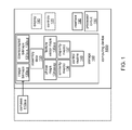
- FIG. 1 illustrates a block diagram of a computing device 1000 externally coupled to and/or internally incorporating cameras 110 a - x .
- the computing device 1000 may be any of a variety of types of computing device, including without limitation, a desktop computer system, a data entry terminal, a laptop computer, a netbook computer, an ultrabook computer, a tablet computer, a handheld personal data assistant, a smartphone, a digital camera, a body-worn computing device incorporated into clothing, a computing device integrated into a vehicle (e.g., a car, a bicycle, a wheelchair, etc.), a server, a cluster of servers, a server farm, etc.
- a vehicle e.g., a car, a bicycle, a wheelchair, etc.
- server e.g., a server, a cluster of servers, a server farm, etc.
- the computing device 1000 may be coupled to any of a variety of other computing devices via a network (not shown).
- That network may be a single network possibly limited to extending within a single building or other relatively limited area, a combination of connected networks possibly extending a considerable distance, and/or may include the Internet.
- a network may be based on any of a variety (or combination) of communications technologies by which signals may be exchanged, including without limitation, wired technologies employing electrically and/or optically conductive cabling, and wireless technologies employing infrared, radio frequency or other forms of wireless transmission.
- the computing device 1000 incorporates one or more of a processor circuit 150 , a storage 160 , controls 120 , a display 180 , and an interface 190 .
- the cameras 110 a - x though coupled to the computing device 1000 to convey captured images thereto, are not incorporated into the computing device 1000 , itself.
- the cameras 110 a - x may be coupled to the computing device 1000 via a network to which the computing device 1000 is also coupled via the interface 190 , possibly the very same network by which the computing device 1000 may exchange data with one or more other computing devices.
- the cameras 110 a - x are incorporated into the computing device 1000 .
- the cameras 110 a - x may include a single camera operated to capture multiple images of a common scene with a recurring interval of time between image captures.
- the cameras 110 a - x include two or more cameras forming an array to capture images of a common scene from different vantage points substantially simultaneously, thereby providing at least binocular image capture.
- the storage 160 stores at least the control routine 140 and one or more of image bitmaps 130 a - x , downsampled bitmaps 131 a - x and 132 a - x , phase maps 134 aa - xy , feature vector maps 135 a - x , similarity map(s) 136 , and disparity map(s) 137 .
- An assembly data 133 may also be stored in the storage 160 and/or may be carried by a camera array formed from the cameras 110 a - x .
- the similarity maps 136 ( s ) may include one or more similarity maps depending on whether there are two or more of the cameras 1110 a - x .
- the disparity map(s) 137 may include one or more disparity maps depending on whether at least a second disparity map is generated for consistency checking.
- the processor circuit 150 In executing the control routine 140 , the processor circuit 150 is caused to receive multiple captured images captured by the cameras 110 a - x , and store them as corresponding ones of the image bitmaps 130 a - x . The processor circuit 150 then creates levels of downsampled versions of each of the captured images of the image bitmaps 130 a - x , storing a first level of the downsampled versions as corresponding ones downsampled bitmaps 131 a - x , and possibly storing a second level of the downsampled versions as corresponding ones of downsampled bitmaps 132 a - x.
- the processor circuit 150 is then caused to subject each of the image bitmaps 130 a - x and each of corresponding ones of the downsampled bitmaps 131 a - x and 132 a - x , multiple times, to both first and second order wavelet filters set to different orientations to derive the phase maps 134 aa - xy indicative of distances of each pixel to edges in different directions.
- the processor circuit 150 is then caused to combine all of the phase maps of each one of the image bitmaps 130 a - x and its corresponding ones of the downsample bitmaps 131 a - x and 132 a - x into one of the feature vector maps 135 a - x , such that each of the feature vector maps 135 a - x corresponds to one of the image bitmaps 130 a - x , respectively.
- One of the feature vector maps 135 a - x is then designated as a first reference feature vector map to which the other ones of the feature vector maps 135 a - x are compared by the processor circuit 150 in a first set of comparisons.
- Each such comparison generates a similarity map of a first set of similarity maps (possibly the only set of similarity maps) that is stored as part of the similarity map(s) 136 .
- the first set of similarity maps stored as the similarity maps 136 includes more than one similarity map.
- the multiple similarity maps are analyzed together, taking into account the assembly data 133 specifying the relative positions and orientations of the vantage points of the cameras 110 a - x from which each of the image bitmaps 130 a - x were captured, to derive a single disparity map. Where this single disparity map is not to be subjected to consistency checking, this single disparity map becomes the final disparity map.
- another one of the feature vector maps 135 a - x is designated as a second reference feature vector map to which the others of the feature vector maps 135 a - x are compared by the processor circuit 150 in a second set of comparisons.
- Each such comparison generates a similarity map of a second set of similarity maps that is also stored as part of the similarity map(s) 136 (along with the first set of similarity maps).
- the multiple similarity maps of this second set of similarity maps are analyzed together, again taking into account the assembly data 133 , to derive a second single disparity map.
- These two disparity maps of the disparity map(s) 137 are then subjected to a consistency check that employs information in the assembly data 133 . Presuming a selected threshold of consistency is found to be met, either one of these two disparity maps making up the disparity map(s) 137 may then be designated as the final disparity map.
- the processor circuit 150 may include any of a wide variety of commercially available processors, including without limitation, an AMD® Athlon®, Duron® or Opteron® processor; an ARM® application, embedded or secure processor; an IBM® and/or Motorola® DragonBall® or PowerPC® processor; an IBM and/or Sony® Cell processor; or an Intel® Celeron®, Core (2) Duo®, Core (2) Quad®, Core i3®, Core i5®, Core i7®, Atom®, Itanium®, Pentium®, Xeon® or XScale® processor. Further, one or more of these processor circuits may include a multi-core processor (whether the multiple cores coexist on the same or separate dies), and/or a multi-processor architecture of some other variety by which multiple physically separate processors are in some way linked.
- the storage 160 may be based on any of a wide variety of information storage technologies, possibly including volatile technologies requiring the uninterrupted provision of electric power, and possibly including technologies entailing the use of machine-readable storage media that may or may not be removable.
- each of these storages may include any of a wide variety of types (or combination of types) of storage device, including without limitation, read-only memory (ROM), random-access memory (RAM), dynamic RAM (DRAM), Double-Data-Rate DRAM (DDR-DRAM), synchronous DRAM (SDRAM), static RAM (SRAM), programmable ROM (PROM), erasable programmable ROM (EPROM), electrically erasable programmable ROM (EEPROM), flash memory, polymer memory (e.g., ferroelectric polymer memory), ovonic memory, phase change or ferroelectric memory, silicon-oxide-nitride-oxide-silicon (SONOS) memory, magnetic or optical cards, one or more individual ferromagnetic disk drives, or a plurality of storage
- ROM
- each of these storages is depicted as a single block, one or more of these may be made up of multiple storage devices that may be based on differing storage technologies.
- one or more of each of these depicted storages may represent a combination of an optical drive or flash memory card reader by which programs and/or data may be stored and conveyed on some form of machine-readable storage media, a ferromagnetic disk drive to store programs and/or data locally for a relatively extended period, and one or more volatile solid state memory devices enabling relatively quick access to programs and/or data (e.g., SRAM or DRAM).
- each of these storages may be made up of multiple storage components based on identical storage technology, but which may be maintained separately as a result of specialization in use (e.g., some DRAM devices employed as a main storage while other DRAM devices employed as a distinct frame buffer of a graphics controller).
- the interface 190 may employ any of a wide variety of signaling technologies enabling the computing device 1000 to be coupled to other devices as has been described. Each of these interfaces includes circuitry providing at least some of the requisite functionality to enable such coupling. However, this interface may also be at least partially implemented with sequences of instructions executed by the processor circuit 150 (e.g., to implement a protocol stack or other features). Where electrically and/or optically conductive cabling is employed, these interfaces may employ signaling and/or protocols conforming to any of a variety of industry standards, including without limitation, RS-232C, RS-422, USB, Ethernet (IEEE-802.3) or IEEE-1394.
- these interfaces may employ signaling and/or protocols conforming to any of a variety of industry standards, including without limitation, IEEE 802.11a, 802.11b, 802.11g, 802.16, 802.20 (commonly referred to as “Mobile Broadband Wireless Access”); Bluetooth; ZigBee; or a cellular radiotelephone service such as GSM with General Packet Radio Service (GSM/GPRS), CDMA/1xRTT, Enhanced Data Rates for Global Evolution (EDGE), Evolution Data Only/Optimized (EV-DO), Evolution For Data and Voice (EV-DV), High Speed Downlink Packet Access (HSDPA), High Speed Uplink Packet Access (HSUPA), 4G LTE, etc.
- GSM General Packet Radio Service
- EDGE Enhanced Data Rates for Global Evolution
- EV-DO Evolution Data Only/Optimized
- EV-DV Evolution For Data and Voice
- HSDPA High Speed Downlink Packet Access
- HSUPA High Speed Uplink Packet Access
- 4G LTE etc.
- FIG. 2 illustrates a block diagram of portions of the block diagram of FIG. 1 depicted in greater detail. More specifically, aspects of the operating environments of the computing device 1000 are depicted, in which the processor circuit 150 ( FIG. 1 ) is caused by execution of the control routine 140 to perform the aforedescribed functions. As will be recognized by those skilled in the art, the control routine 140 , including the components of which it is composed, are selected to be operative on whatever type of processor or processors that are selected to implement the processor circuit 150 . Further, FIGS.
- 3 a - b , 4 a - b , 5 , 6 , 7 and 8 each depict aspects of operation of components of the control routine 140 through the presentation of an example embodiment including four cameras 110 a - d forming an example 1 ⁇ 4 camera array 111 ( FIG. 3 b ) that each capture an image that is stored as a corresponding one of images bitmaps 130 a - d .
- this example entails the use of four cameras substantially simultaneously capturing images of a common scene, other embodiments are possible employing other quantities of multiple cameras or employing a single camera capturing multiple images over a period of time.
- these four cameras 110 a - d are depicted as organized into a 1 ⁇ 4 array, other embodiments are possible in which these same four cameras (or any number of cameras 110 a - x ) may be physically positioned relative to each other in any of a number of ways, including and not limited to, a 2 ⁇ 2, a “T” or “L” arrangement, etc.
- control routine 140 may include a combination of an operating system, device drivers and/or application-level routines (e.g., so-called “software suites” provided on disc media, “applets” obtained from a remote server, etc.).
- an operating system may be any of a variety of available operating systems appropriate for whatever corresponding ones of the processor circuits 150 and 350 , including without limitation, WindowsTM, OS XTM, Linux®, or Android OSTM.
- those device drivers may provide support for any of a variety of other components, whether hardware or software components, that include the computing devices 1000 .
- the control routine 140 includes a communications component 149 executable by the processor circuit 150 to operate the interface 190 transmit and receive signals via the network 999 as has been described.
- each of these communications components are selected to be operable with whatever type of interface technology is selected to implement each of the corresponding ones of these interfaces.
- the control routine 140 includes a downsampling component 141 executable by the processor circuit 150 to create multiple levels of downsampled versions of each of the image bitmaps 130 a - d . Specifically, and turning momentarily to FIG. 3 a , each of the image bitmaps 130 a through 130 d are downsampled once to create downsampled bitmaps 131 a through 131 d , and then downsampled again to create downsampled bitmaps 132 a through 132 d , respectively. In such downsampling, conceivably any ratio of an original quantity of pixels to a downsampled quantity of pixels may be used.
- the first level of downsampling causes 2 ⁇ 2 arrays of four pixels in each of the image bitmaps 130 a - d to be downsampled to a single pixel in corresponding ones of the downsampled bitmaps 131 a - d .
- the second level of downsampling causes 2 ⁇ 2 arrays of four pixels in each of the downsampled bitmaps 131 a - d to be downsampled to a single pixel in corresponding ones of the downsampled bitmaps 132 a - d .
- Such progressive downsampling of bitmaps from higher resolutions to lower resolutions is sometimes referred to as “pyramid image processing.”
- the color, intensity and/or other per-pixel values associated with each of the multiple pixels that are downsampled to just one pixel are averaged, and the resulting single pixel is given those averaged values.
- the values associated with only one of the multiple pixels that are downsampled are copied and given to the resulting single pixel, while the values associated with all of the others of those multiple pixels are not carried over to the resulting single pixel in any way.
- This latter variant of handling pixel values in downsampling is sometimes referred to as “decimation,” since the values of only some pixels in the original bitmap are carried over to the resulting downsampled bitmap while the others are ignored.
- the downsampled bitmaps 131 a - d and 132 a - d necessarily provide less information than the originally captured image bitmaps 130 a - d , respectively.
- these “coarser” representations of the captured images created by downsampling have the benefit of allowing an edge identification algorithm to focus on identifying the edges of larger objects, since the downsampling often results in the discarding of data enabling identification of edges of smaller objects. Stated differently, smaller objects become blurred or indistinct enough that their presence no longer distracts from identifying features of larger objects that are more likely to remain distinguishable in downsampled bitmaps.
- FIG. 3 a Although two levels of downsampling are depicted in FIG. 3 a , other embodiments are possible in which there may be any number of levels of downsampling. As those skilled in the art will readily recognize, there are diminishing returns in terms of the benefits afforded by continuing to increase the number of levels of downsampling, and what number of levels is useful is partially a function of the resolution of the original image. Thus, it is envisioned that a number of levels of downsampling will be determined through consideration of the resolution of the image bitmaps 130 a - d along with how many levels are needed to aid in detection of lines of larger objects given the type of scenery that is expected to be captured in the bitmap images 130 a - d.
- control routine 140 includes a wavelet filtering component 144 executable by the processor circuit 150 to subject each of the image bitmaps 130 a - x and corresponding ones of the downsampled bitmaps, multiple times, to both first and second order wavelet filters set to different orientations each time to derive phase maps indicative of distances of each pixel to an edge in different directions.
- a wavelet filtering component 144 executable by the processor circuit 150 to subject each of the image bitmaps 130 a - x and corresponding ones of the downsampled bitmaps, multiple times, to both first and second order wavelet filters set to different orientations each time to derive phase maps indicative of distances of each pixel to an edge in different directions.
- the image bitmap 130 a and its downsampled bitmaps 131 a and 132 a are subjected to wavelet filters to derive the phase maps 134 aa - ac ;
- the image bitmap 130 b and its downsampled bitmaps 131 b and 132 b are subjected to wavelet filters to derive the phase maps 134 ba - bc ;
- the image bitmap 130 c and its downsampled bitmaps 131 c and 132 c are subjected to wavelet filters to derive the phase maps 134 ca - cc ;
- the image bitmap 130 d and its downsampled bitmaps 131 d and 132 d are subjected to wavelet filters to derive the phase maps 134 da - dc.
- FIG. 4 b provides further detail of the operation of the wavelet component 144 performing a portion of what is depicted in FIG. 4 a in deriving the phase maps 134 ab from the image bitmap 130 a .
- the wavelet component includes both a first-order wavelet filter 1441 and a second-order wavelet filter 1442 .
- the image bitmap 130 a is convolved using both of the first-order wavelet filter 1441 and the second-order wavelet filter 1442 multiple times, thereby creating multiple ones of intermediate maps 1341 and 1342 , respectively.
- Each of the wavelet filters 1441 and 1442 transform the bitmap information of each pixel of the image bitmap 130 a into the frequency domain, providing a scalar value for each pixel in each of these intermediate maps that indicates a distance from an edge in a given direction from that pixel, the given direction set by the orientation to which the first-order wavelet filter 1441 and the second-order wavelet filter 1442 have been set.
- the orientations of these wavelet filters are changed to enable determination of the distance of each pixel from an edge in a different direction.
- the specific wavelet functions of these two wavelet filters and the orientations given to each of them may be chosen to be mathematically related such that the first-order wavelet filter 1441 approximates a “sine” function masked by a Gaussian and the second-order wavelet filter 1442 approximates a related “cosine” function masked by a Gaussian of the same phase in the frequency domain.
- the first-order wavelet filter 1441 provides a scalar value for each pixel indicating how far that pixel is from a “step” edge
- the second-order wavelet filter 1442 provides a scalar value for each pixel indicating how far that pixel is from a “bar” edge.
- each of the intermediate maps 1341 and 1342 are made up of scalar values indicative of distances to step and bar edges in various directions, respectively.
- FIG. 4 b depicts subjecting the image bitmap 130 a to both of these two wavelet filters five times (creating five each of the intermediate maps 1341 and 1342 ), each time with these two wavelet filters set to different orientations
- each of the bitmaps 130 a - d and the downsampled 131 a - d and 132 a - d are subjected to a greater or lesser number of times to these two wavelet filters. This is based entirely on the number of orientations selected for each of these two wavelet filters to use. A greater number of orientations may be deemed desirable where the captured images are expected to have greater complexity, and thus, more edges. A greater quantity of edges in an image likely requires more data points to describe effectively, likely requiring these two wavelet filters to be set to a greater number of orientations, resulting a greater quantity of intermediate maps (and a corresponding quantity of phase maps) for each image.
- the wavelet component 144 also includes a ratio calculator 1444 to calculate ratios of the scalar values of each pixel in corresponding ones of the intermediate maps 1341 and 1342 .
- the ratio calculator creates phase maps made up of ratio values for each pixel indicative of distances to the nearest edge (of whatever type) in the various directions corresponding to the various orientations to which the first-order wavelet filter 1441 and the second-order wavelet filter 1442 were set (specifically, the phase maps 134 ab corresponding to the image bitmap 130 a ).
- These ratio values are each a continuous measure of the proximity of an edge in which a value of zero indicates that the particular pixel overlies an edge, and a non-zero value is indicative of a relative distance to an edge.
- control routine 140 includes a combining component 145 executable by the processor circuit 150 to combine the indications of distances to edges of each original pixel and coarser downsampled counterpart pixels into sets of feature vectors for each pixel within a feature vector map.
- all of the per-pixel values indicative of distances from edges in various directions in each of the phase maps 134 aa - ac are combined into a list of feature vectors indicating distances and directions of edges for each pixel in the feature vector map 135 a ; such per-pixel information in each of the phase maps 134 ba - bc are combined into such a list of vectors in the feature vector map 135 b ; such per-pixel information in each of the phase maps 134 ca - cc are combined into such a list of vectors in the feature vector map 135 c ; and such per-pixel information in each of the phase maps 134 da - dc are combined into such a list of vectors in the feature vector map 135 d.
- phase maps 135 a - d since some of these phase maps were generated from downsampled bitmaps of the original captured images, each of their coarser pixels overlie multiple ones of the original captured image pixels. Thus, the feature vectors contributed by each of these coarser pixels will each be incorporated into all of the original-sized pixels that they overlie in the feature vector maps 135 a - d.
- the control routine 140 includes a comparing component 146 executable by the processor circuit 150 to perform at least a first set of comparisons among the feature vector maps 135 a - d to create a first set of similarity maps 1361 ab , 1361 ac and 1361 ad making up the similarity maps 136 .
- the feature vector map 135 a is selected to be a first reference feature vector map against which each of the other feature vector maps 135 b - d is compared in this first set of comparisons.
- each pixel of the feature vector map 135 a (the first reference) is compared to the pixel at the corresponding location and at neighboring locations in each of the feature vector maps 135 b - d .
- the degree to which the feature vector values of each of those pixels at the corresponding and neighboring locations in each of the feature vector maps 135 b - d are similar to the feature vector values of the pixel of the feature vector map 135 a is stored as a set of similarity values in separate similarity maps that each correspond to one of the compared pairs of feature vector maps.
- the degree to which the feature vector values of a pixel of the feature vector map 135 a (the first reference) are similar to the feature vector values of the pixel at the corresponding location and at the locations neighboring that corresponding location in the feature vector map 135 b are stored as a set of similarity values for that pixel of the feature vector map 135 a in the similarity map 1361 ab .
- Similarity values from comparisons between the feature vector maps 135 a and 135 c are stored in the similarity map 1361 ac
- similarity values from comparisons between the feature vector maps 135 a and 135 d are stored in the similarity map 1361 ad .
- the comparing component 146 employs indications in the assembly data 133 of the relative positions of each of the cameras 110 a - d to at least partly determine what neighboring pixel locations in each of the feature vector maps 135 b - d to include in these comparisons to derive similarity values for inclusion in each of the similarity maps 1361 ab , 1361 ac and 1361 ad.
- the feature vector map 135 d may be selected as a second reference feature vector map against which each of the others of the feature vector maps 135 a - c is compared in an optional second set of comparisons (the optional nature of which is indicated via the use of dotted lines) creating a second set of similarity maps 1362 dc , 1362 db and 1362 da making up more of the similarity map(s) 136 .
- the feature vector values of each pixel of the feature vector map 135 d (the second reference) are compared to the feature vector values of the pixel at the corresponding location and at neighboring locations in each of the feature vector maps 135 a - c .
- the degree to which the feature vector values of the pixels at those corresponding locations and at the neighboring locations in each of the feature vector maps 135 a - c are similar to the feature vector values of each pixel of the feature vector map 135 d is stored as sets of similarity values in separate similarity maps that correspond to each pair of compared feature vector maps.
- similarity values from comparisons between the feature vector maps 135 d and 135 c are stored in the similarity map 1362 dc
- similarity values from comparisons between the feature vector maps 135 d and 135 b are stored in the similarity map 1362 db
- similarity values from comparisons between the feature vector maps 135 d and 135 a are stored in the similarity map 1362 da.
- comparing component 146 is depicted as including multiple comparators, three of comparators 1461 for performing each feature vector map comparison of the first set of comparisons and three comparators 1462 for performing each feature vector map comparison of the second set of comparisons, other embodiments are possible in which requisite comparison logic may be implemented in any of a number of ways. Indeed, a single pixel-by-pixel feature vector comparator may be implemented and iteratively used in some embodiments to compare corresponding feature vector values, one-by-one and pixel-by-pixel, while banks of comparators may be employed in other embodiments to achieve greater performance via some degree of parallelism.
- control routine 140 includes a disparity component 147 executable by the processor circuit 150 to analyze at least the first set of similarity maps 1361 ab , 1361 ac and 1361 ad of the similarity map(s) 136 to derive at least at a first disparity map 1371 of the disparity map(s) 137 . More specifically, and turning momentarily to FIG.
- the relative positions of the cameras 110 a - d are such that the camera 110 b is the immediate neighbor of the camera 110 a , with the camera 110 c just beyond the camera 110 b from the camera 110 a , and with the camera 110 d just beyond both of the cameras 110 b and 110 c from the camera 110 a .
- the distances 116 between adjacent ones the optic centers 115 of each of the cameras 110 a - d are equal.
- this information from the assembly data 133 leads to an expectation that distances (measured in pixels) between corresponding pixels of the feature vector maps 135 a and 135 c should generally be twice that of distances between corresponding pixels of the feature vector maps 135 a and 135 b , and similarly, distances between corresponding pixels of the feature vector maps 135 a and 135 d should generally be three times that of distances between corresponding pixels of the feature vectors maps 135 a and 135 b .
- the information on relative distances between the optic centers 115 of the cameras 110 a - d in the assembly data 133 should indicate proportions of distances that should be reflected in the analysis of the first set of similarity maps.
- FIG. 7 b aspects are graphically depicted of the data stored in each of the similarity maps 1361 ab , 1361 ac and 1361 ad that indicates the results of comparisons of feature vector values between a single pixel of the feature vector map 135 a and pixels at both corresponding and neighboring locations in each of the feature vector maps 135 b - d .
- the similarity map 1361 ab from the location of the pixel of the feature vector map 135 a there appears to be a pixel two pixels away in the feature vector map 135 b that may correspond to the pixel of the feature vector map 135 a .
- This pixel at two pixels away in the feature vector map 135 b is found to have feature vector values that are relatively similar to those of the pixel of the feature vector map 135 a .
- This pixel at four pixels away in the feature vector map 135 c is found to have feature vector values that are relatively similar to those of the pixel of the feature vector map 135 a .
- the relative distances (as measured in pixels) between the location of the pixel of the feature vector map 135 a and the locations of each of these possible corresponding pixels of in feature vector maps 135 b and 135 c have the same relative proportions as the distances between the optic center 115 of the camera 110 a and the optic centers 115 of each of the cameras 110 b and 110 c , respectively.
- this correspondence of proportions of distances is taken as tending to confirm that these two pixels in the feature vector maps 135 b and 135 c must correspond to the pixel of the feature vector map 135 a.
- the relative proportion of the distance between the location of the pixel of the feature vector map 135 a and the location of this possible corresponding pixel in the feature vector map 135 d also fits the relative proportions of the distance between the optic center 115 of the camera 110 a and the optic center 115 of the camera 110 d , taken in conjunction with the other aforementioned distances between optic centers.
- further confirmation is provided that enables the determination that these pixels at two, four and six pixels away in the feature vector maps 135 b , 135 c and 135 d , respectively, from the location of the pixel of the feature vector map 135 a are, indeed, the pixels that correspond to the pixel of the feature vector map 135 a.
- the disparity component 147 derives the disparity value in the disparity map 1371 that corresponds to the pixel of the feature vector map 135 a to be two, as this is the distance in pixels from the location of the pixel of the feature vector map 135 a to its closest corresponding pixel, namely its corresponding pixel in the feature vector map 135 b .
- the disparity component 147 is also executable by the processor circuit 150 to subject that second set of similarity maps (namely, the similarity maps 1362 dc , 1362 db and 1362 da ) to the same analysis to derive a second disparity map of the disparity map(s) 137 (namely, the disparity map 1372 ).
- the control routine 140 may include a consistency component 148 executable by the processor circuit 150 to subject the first and second final disparity maps 1371 and 1372 stored as the disparity map(s) 137 to a comparison of their disparity values, taking into account the relative proportions of distances between the optic centers of the cameras 110 a - d , as indicated in the assembly data 133 . Where consistency meeting a selected threshold is found between the two disparity maps 1371 and 1372 , either disparity map may then be used as the final disparity map to be provided as in input to whatever other computer vision or image processing functions are to be performed.
- such further processing functions may be performed by the processor circuit 150 and may culminate in the processor circuit 150 causing a three-dimensional image (or portions thereof) to be visually presented on the display 180 , in some embodiments.
- the processor circuit 150 may be caused to operate the interface 190 to transmit data representing imagery derived (at least in part) from the final disparity map to another computing device (not shown) via a network (not shown), either in lieu of or in addition to transmitting the final disparity map itself via that network.
- FIG. 8 illustrates an embodiment of a logic flow 2100 .
- the logic flow 2100 may be representative of some or all of the operations executed by one or more embodiments described herein. More specifically, the logic flow 2100 may illustrate operations performed by at least the processor circuit 150 of the computing device 1000 in executing at least the control routine 140 .
- a computing device receives multiple captured image bitmaps from either a single camera employed to capture the multiple image bitmaps over time or multiple cameras employed to capture the multiple images substantially simultaneously (e.g., the cameras 110 a - x ).
- a computing device receives multiple captured image bitmaps from either a single camera employed to capture the multiple image bitmaps over time or multiple cameras employed to capture the multiple images substantially simultaneously (e.g., the cameras 110 a - x ).
- those cameras may be arranged in any of a variety of ways including any of a number of arrangements of camera array.
- the computing device downsamples each of the captured image bitmaps (e.g., the image bitmaps 130 a - x ) to a selected number of levels of pyramid image processing to create that selected number of levels of downsampled bitmaps (e.g., the two levels of downsampled bitmaps 131 a - x , 132 a - x depicted in examples herein).
- the number of levels selected is at least partially dependent on the resolution and/or expected complexity of the captured image bitmaps.
- FIG. 9 illustrates an embodiment of a logic flow 2200 .
- the logic flow 2200 may be representative of some or all of the operations executed by one or more embodiments described herein. More specifically, the logic flow 2200 may illustrate operations performed by at least the processor circuit 150 of the computing device 1000 in executing at least the control routine 140 .
- a computing device receives a signal conveying a command to the computing device to capture multiple image bitmaps, all of a single common scene.
- a single camera operated to capture each of the multiple image bitmaps over time or multiple cameras operated to capture the multiple image bitmaps substantially simultaneously may be used (e.g., the cameras 110 a - x ).
- the computing device operates the camera(s) to capture the multiple image bitmaps.
- those cameras may be arranged in any of a variety of ways including any of a number of arrangements of camera array.
- the computing device downsamples each of the captured image bitmaps (e.g., the image bitmaps 130 a - x ) to a selected number of levels of pyramid image processing to create that selected number of levels of downsampled bitmaps (e.g., the two levels of downsampled bitmaps 131 a - x , 132 a - x depicted in examples herein).
- the number of levels selected is at least partially dependent on the resolution and/or expected complexity of the captured image bitmaps.
- FIG. 10 illustrates an embodiment of a logic flow 2300 .
- the logic flow 2300 may be representative of some or all of the operations executed by one or more embodiments described herein. More specifically, the logic flow 2300 may illustrate operations performed by at least the processor circuit 150 of the computing device 1000 in executing at least the control routine 140 .
- a computing device implements a first-order wavelet filter (e.g., the first-order wavelet filter 1441 ), and subjects each image bitmap and downsampled bitmap to the first-order wavelet filter multiple times, with the first-order wavelet filter set to different selected orientation each time, to create intermediate maps indicative of distances of each pixel to a step edge in different directions corresponding to the different orientations (e.g., the intermediate maps 1341 ).
- a first-order wavelet filter e.g., the first-order wavelet filter 1441
- the computing device implements a second-order wavelet filter (e.g., the second-order wavelet filter 1442 ), and subjects each of the same image bitmaps and downsampled bitmaps to the second-order wavelet filter multiple times, with the second-order wavelet filter set to different selected orientation each time, to create intermediate maps indicative of distances of each pixel to a bar edge in different directions corresponding to the different orientations (e.g., the intermediate maps 1342 ).
- a second-order wavelet filter e.g., the second-order wavelet filter 1442
- the wavelet transforms implemented by each of the first-order and second-order filters, as well as the multiple orientations to which each is set, may be selected to be mathematically related such that the first-order wavelet filter approximates a “sine” function masked by a Gaussian and the second-order wavelet filter approximates a related “cosine” function also masked by a Gaussian.
- pixel-by-pixel ratios are taken from corresponding ones of the intermediate maps generated by the first-order and second-order filters to create phase maps that include the ratios for each pixel (e.g., the phase maps 134 aa - xy ). As previously discussed, the ratios are indicative of distances from each pixel to any form of edge.
- a single feature vector map made up of a list of feature vectors indicative of the ratios and associated directions for each pixel (e.g., the feature vector maps 135 a - x ).
- the creation of these feature vector maps is the reversal of the repeated splitting apart of data derived from each of the originally captured image bitmaps—the result is a one-to-one correspondence of image bitmaps to feature vector maps.
- FIG. 11 illustrates an embodiment of a logic flow 2400 .
- the logic flow 2400 may be representative of some or all of the operations executed by one or more embodiments described herein. More specifically, the logic flow 2400 may illustrate operations performed by at least the processor circuit 150 of the computing device 1000 in executing at least the control routine 140 .
- a computing device selects a feature vector map of multiple feature vector maps (e.g., the feature vector maps 135 a - x ) that have been created by combining multiple phase maps to be a reference.
- the computing device compares all others of the multiple feature vector maps to that reference, creating one or more similarity maps (e.g., the similarity map(s) 136 ) depending on the number of feature vector maps.
- each of the similarity maps is made up of sets of similarity values from comparisons of pixels of the reference to pixels at the corresponding and neighboring locations in each of the other feature vector maps.
- a check is made as to whether there is more than one similarity map. If not, as would be the case where there were originally only two captured image bitmaps, then the one similarity map is used to derive the final disparity map for use in further computer vision or image processing at 2422 . As has been discussed, such further processing may be performed by this same computing device, possibly culminating in the computing device visually presenting possibly a three-dimension image derived from the final disparity map, or may be performed by another computing device to which this computing device transmits the final disparity map (or other data derived therefrom) via a network.
- the computing device analyzes each of the similarity maps to locate corresponding pixels located at distances proportional to distance between optical centers of the cameras used to capture the image bitmaps from the locations of pixels of the reference to derive the final disparity map.
- an assembly data describing such aspects of relative placement of multiple cameras or relative positions of vantage points used by one camera.
- FIG. 12 illustrates an embodiment of an exemplary processing architecture 3100 suitable for implementing various embodiments as previously described. More specifically, the processing architecture 3100 (or variants thereof) may be implemented as part of the computing device 1000 . It should be noted that components of the processing architecture 3100 are given reference numbers in which the last two digits correspond to the last two digits of reference numbers of components earlier depicted and described as part of the computing device 1000 . This is done as an aid to correlating such components of the computing device 1000 may employ this exemplary processing architecture in various embodiments.
- the processing architecture 3100 includes various elements commonly employed in digital processing, including without limitation, one or more processors, multi-core processors, co-processors, memory units, chipsets, controllers, peripherals, interfaces, oscillators, timing devices, video cards, audio cards, multimedia input/output (I/O) components, power supplies, etc.
- system and “component” are intended to refer to an entity of a computing device in which digital processing is carried out, that entity being hardware, a combination of hardware and software, software, or software in execution, examples of which are provided by this depicted exemplary processing architecture.
- a component can be, but is not limited to being, a process running on a processor circuit, the processor circuit itself, a storage device (e.g., a hard disk drive, multiple storage drives in an array, etc.) that may employ an optical and/or magnetic storage medium, an software object, an executable sequence of instructions, a thread of execution, a program, and/or an entire computing device (e.g., an entire computer).
- a component can be, but is not limited to being, a process running on a processor circuit, the processor circuit itself, a storage device (e.g., a hard disk drive, multiple storage drives in an array, etc.) that may employ an optical and/or magnetic storage medium, an software object, an executable sequence of instructions, a thread of execution, a program, and/or an entire computing device (e.g., an entire computer).
- an application running on a server and the server can be a component.
- One or more components can reside within a process and/or thread of execution, and a component can be local
- the coordination may involve the uni-directional or bi-directional exchange of information.
- the components may communicate information in the form of signals communicated over the communications media.
- the information can be implemented as signals allocated to one or more signal lines.
- a message (including a command, status, address or data message) may be one of such signals or may be a plurality of such signals, and may be transmitted either serially or substantially in parallel through any of a variety of connections and/or interfaces.
- a computing device incorporates at least a processor circuit 950 , support logic 951 , a storage 960 , a controller 900 , an interface 990 to other devices, and coupling 955 .
- a computing device may further include additional components, such as without limitation, a display interface 985 and/or one or more cameras 910 .
- Coupling 955 is made up of one or more buses, point-to-point interconnects, transceivers, buffers, crosspoint switches, and/or other conductors and/or logic that communicatively couples at least the processor circuit 950 to the storage 960 . Coupling 955 may further couple the processor circuit 950 to one or more of the interface 990 , the audio subsystem 970 and the display interface 985 (depending on which of these and/or other components are also present). With the processor circuit 950 being so coupled by couplings 955 , the processor circuit 950 is able to perform the various ones of the tasks described at length, above, for whichever ones of the computing device 1000 and the controller 200 implement the processing architecture 3100 .
- Coupling 955 may be implemented with any of a variety of technologies or combinations of technologies by which signals are optically and/or electrically conveyed. Further, at least portions of couplings 955 may employ timings and/or protocols conforming to any of a wide variety of industry standards, including without limitation, Accelerated Graphics Port (AGP), CardBus, Extended Industry Standard Architecture (E-ISA), Micro Channel Architecture (MCA), NuBus, Peripheral Component Interconnect (Extended) (PCI-X), PCI Express (PCI-E), Personal Computer Memory Card International Association (PCMCIA) bus, HyperTransportTM, QuickPath, and the like.
- AGP Accelerated Graphics Port
- CardBus Extended Industry Standard Architecture
- MCA Micro Channel Architecture
- NuBus NuBus
- PCI-X Peripheral Component Interconnect
- PCI-E PCI Express
- PCMCIA Personal Computer Memory Card International Association
- the processor circuit 950 (corresponding to the processor circuit 150 ) may include any of a wide variety of commercially available processors, employing any of a wide variety of technologies and implemented with one or more cores physically combined in any of a number of ways.
- the storage 960 may include one or more distinct storage devices based on any of a wide variety of technologies or combinations of technologies. More specifically, as depicted, the storage 960 may include one or more of a volatile storage 961 (e.g., solid state storage based on one or more forms of RAM technology), a non-volatile storage 962 (e.g., solid state, ferromagnetic or other storage not requiring a constant provision of electric power to preserve their contents), and a removable media storage 963 (e.g., removable disc or solid state memory card storage by which information may be conveyed between computing devices).
- a volatile storage 961 e.g., solid state storage based on one or more forms of RAM technology
- a non-volatile storage 962 e.g., solid state, ferromagnetic or other storage not requiring a constant provision of electric power to preserve their contents
- a removable media storage 963 e.g., removable disc or solid state memory card storage by which information may be conveyed between computing devices.
- This depiction of the storage 960 as possibly including multiple distinct types of storage is in recognition of the commonplace use of more than one type of storage device in computing devices in which one type provides relatively rapid reading and writing capabilities enabling more rapid manipulation of data by the processor circuit 950 (but possibly using a “volatile” technology constantly requiring electric power) while another type provides relatively high density of non-volatile storage (but likely provides relatively slow reading and writing capabilities).
- the volatile storage 961 may be communicatively coupled to coupling 955 through a storage controller 965 a providing an appropriate interface to the volatile storage 961 that perhaps employs row and column addressing, and where the storage controller 965 a may perform row refreshing and/or other maintenance tasks to aid in preserving information stored within the volatile storage 961 .
- the non-volatile storage 962 may be communicatively coupled to coupling 955 through a storage controller 965 b providing an appropriate interface to the non-volatile storage 962 that perhaps employs addressing of blocks of information and/or of cylinders and sectors.
- the removable media storage 963 may be communicatively coupled to coupling 955 through a storage controller 965 c providing an appropriate interface to the removable media storage 963 that perhaps employs addressing of blocks of information, and where the storage controller 965 c may coordinate read, erase and write operations in a manner specific to extending the lifespan of the machine-readable storage medium 969 .
- One or the other of the volatile storage 961 or the non-volatile storage 962 may include an article of manufacture in the form of a machine-readable storage media on which a routine including a sequence of instructions executable by the processor circuit 950 may be stored, depending on the technologies on which each is based.
- the non-volatile storage 962 includes ferromagnetic-based disk drives (e.g., so-called “hard drives”)
- each such disk drive typically employs one or more rotating platters on which a coating of magnetically responsive particles is deposited and magnetically oriented in various patterns to store information, such as a sequence of instructions, in a manner akin to storage medium such as a floppy diskette.
- the non-volatile storage 962 may include banks of solid-state storage devices to store information, such as sequences of instructions, in a manner akin to a compact flash card. Again, it is commonplace to employ differing types of storage devices in a computing device at different times to store executable routines and/or data. Thus, a routine including a sequence of instructions to be executed by the processor circuit 950 may initially be stored on the machine-readable storage medium 969 , and the removable media storage 963 may be subsequently employed in copying that routine to the non-volatile storage 962 for longer term storage not requiring the continuing presence of the machine-readable storage medium 969 and/or the volatile storage 961 to enable more rapid access by the processor circuit 950 as that routine is executed.
- the interface 990 may employ any of a variety of signaling technologies corresponding to any of a variety of communications technologies that may be employed to communicatively couple a computing device to one or more other devices.
- signaling technologies corresponding to any of a variety of communications technologies that may be employed to communicatively couple a computing device to one or more other devices.
- one or both of various forms of wired or wireless signaling may be employed to enable the processor circuit 950 to interact with input/output devices (e.g., the depicted example keyboard 920 or printer 925 ) and/or other computing devices, possibly through a network (e.g., the network 999 ) or an interconnected set of networks.
- the interface 990 is depicted as including multiple different interface controllers 995 a , 995 b and 995 c .
- the interface controller 995 a may employ any of a variety of types of wired digital serial interface or radio frequency wireless interface to receive serially transmitted messages from user input devices, such as the depicted keyboard 920 .
- the interface controller 995 b may employ any of a variety of cabling-based or wireless signaling, timings and/or protocols to access other computing devices through the depicted network 999 (perhaps a network made up of one or more links, smaller networks, or perhaps the Internet).
- the interface 995 c may employ any of a variety of electrically conductive cabling enabling the use of either serial or parallel signal transmission to convey data to the depicted printer 925 .
- Other examples of devices that may be communicatively coupled through one or more interface controllers of the interface 990 include, without limitation, microphones, remote controls, stylus pens, card readers, finger print readers, virtual reality interaction gloves, graphical input tablets, joysticks, other keyboards, retina scanners, the touch input component of touch screens, trackballs, various sensors, laser printers, inkjet printers, mechanical robots, milling machines, etc.
- a computing device is communicatively coupled to (or perhaps, actually includes) a display (e.g., the depicted example display 980 , corresponding to the display 180 )
- a computing device implementing the processing architecture 3100 may also include the display interface 985 .
- the somewhat specialized additional processing often required in visually displaying various forms of content on a display, as well as the somewhat specialized nature of the cabling-based interfaces used, often makes the provision of a distinct display interface desirable.
- Wired and/or wireless signaling technologies that may be employed by the display interface 985 in a communicative coupling of the display 980 may make use of signaling and/or protocols that conform to any of a variety of industry standards, including without limitation, any of a variety of analog video interfaces, Digital Video Interface (DVI), DisplayPort, etc.
- DVI Digital Video Interface
- DisplayPort etc.
- each of the cameras 910 may be based on any of a variety of image capture technologies, including and not limited to semiconductor-based image sensors such as charge-coupled devices (CCD), etc. As has bee previously discussed, the cameras 910 may be arranged into any of a variety of arrays of cameras all to capture images of substantially the same scene at substantially the same time.
- CCD charge-coupled devices
- the various elements of the computing device 1000 may include various hardware elements, software elements, or a combination of both.
- hardware elements may include devices, logic devices, components, processors, microprocessors, circuits, processor circuits, circuit elements (e.g., transistors, resistors, capacitors, inductors, and so forth), integrated circuits, application specific integrated circuits (ASIC), programmable logic devices (PLD), digital signal processors (DSP), field programmable gate array (FPGA), memory units, logic gates, registers, semiconductor device, chips, microchips, chip sets, and so forth.
- ASIC application specific integrated circuits
- PLD programmable logic devices
- DSP digital signal processors
- FPGA field programmable gate array
- Examples of software elements may include software components, programs, applications, computer programs, application programs, system programs, software development programs, machine programs, operating system software, middleware, firmware, software modules, routines, subroutines, functions, methods, procedures, software interfaces, application program interfaces (API), instruction sets, computing code, computer code, code segments, computer code segments, words, values, symbols, or any combination thereof.
- determining whether an embodiment is implemented using hardware elements and/or software elements may vary in accordance with any number of factors, such as desired computational rate, power levels, heat tolerances, processing cycle budget, input data rates, output data rates, memory resources, data bus speeds and other design or performance constraints, as desired for a given implementation.
- Some embodiments may be described using the expression “one embodiment” or “an embodiment” along with their derivatives. These terms mean that a particular feature, structure, or characteristic described in connection with the embodiment is included in at least one embodiment. The appearances of the phrase “in one embodiment” in various places in the specification are not necessarily all referring to the same embodiment. Further, some embodiments may be described using the expression “coupled” and “connected” along with their derivatives. These terms are not necessarily intended as synonyms for each other. For example, some embodiments may be described using the terms “connected” and/or “coupled” to indicate that two or more elements are in direct physical or electrical contact with each other. The term “coupled,” however, may also mean that two or more elements are not in direct contact with each other, but yet still co-operate or interact with each other.
- An example of a device includes a processor circuit, and a storage communicatively coupled to the processor circuit to store instructions. When executed by the processor circuit the instructions cause the processor circuit to implement a first-order wavelet filter and a second-order wavelet filter; subject a first image bitmap captured of a scene to the first-order wavelet filter a selected number of times, an orientation of the first-order wavelet filter altered each time to create an intermediate map of a first set of intermediate maps; and subject the first image bitmap to the second-order wavelet filter the selected number of times, an orientation of the second-order wavelet filter altered each time to create an intermediate map of a second set of intermediate maps.
- An example of another device includes a first camera to capture a first image bitmap of a scene, a second camera to capture a second image bitmap of the scene, a processor circuit, and a storage communicatively coupled to the processor circuit to store instructions.
- the instructions When executed by the processor circuit the instructions cause the processor circuit to operate the first and second cameras substantially simultaneously to capture the first and second image bitmaps; downsample the first image bitmap a selected number of levels to create at least one downsampled bitmap; subject the first image bitmap to a first-order wavelet filter a selected number of times, an orientation of the first-order wavelet filter altered each time to create an intermediate map of a first set of intermediate maps; and subject the first image bitmap to a second-order wavelet filter the selected number of times, an orientation of the second-order wavelet filter altered each time to create an intermediate map of a second set of intermediate maps, the first-order wavelet filter and the second-order wavelet filter selected to be mathematically related, and the orientations of the first-order wave
- the processor circuit is to create one of a first set of phase maps including per-pixel ratios of values of corresponding pixels of one of the first set of intermediate maps and values of corresponding pixels of one of the second set of intermediate maps, each ratio indicative of a distance of a pixel from an edge in the first image bitmap.
- the processor circuit is to create a first feature vector map including per-pixel indications of distances of each pixel from multiple lines in the first image bitmap indicated by values of corresponding pixels of each phase map of the first set of phase maps, and create a second feature vector map including per-pixel indications of distances of each pixel from multiple lines in the second image bitmap indicated by values of corresponding pixels of each phase map of a second set of phase maps corresponding to the second image bitmap.
- An example of a computer-implemented method includes receiving signals conveying a first image bitmap captured of a scene; receiving signals conveying a second image bitmap captured of the scene; subjecting the first image bitmap to a first-order wavelet filter a selected number of times, an orientation of the first-order wavelet filter altered each time to create an intermediate map of a first set of intermediate maps; and subjecting the first image bitmap to a second-order wavelet filter the selected number of times, an orientation of the second-order wavelet filter altered each time to create an intermediate map of a second set of intermediate maps, the first-order wavelet filter and the second-order wavelet filter selected to be mathematically related, and the orientations of the first-order wavelet filter and the second-order wavelet filter selected to be mathematically related such that the first-order wavelet filter approximates a sine function and the second-order wavelet filter approximates a related cosine function.
- the method includes subjecting the first downsampled bitmap to the first-order wavelet filter the selected number of times, the orientation of the first-order wavelet filter altered each time to create another intermediate map of the first set of intermediate maps; and subjecting the first downsampled bitmap to the second-order wavelet filter the selected number of times, the orientation of the second-order wavelet filter altered each time to create another intermediate map of the second set of intermediate maps.
- any of the above examples of a computer-implemented method in which the method includes creating a first feature vector map including per-pixel indications of distances of each pixel from multiple lines in the first image bitmap indicated by values of corresponding pixels of each phase map of the first set of phase maps; and creating a second feature vector map including per-pixel indications of distances of each pixel from multiple lines in a second image bitmap indicated by values of corresponding pixels of each phase map of a second set of phase maps corresponding to the second image bitmap.
- An example of at least one machine-readable storage medium includes instructions that when executed by a computing device, cause the computing device to operate first and second cameras substantially simultaneously to capture first and second image bitmaps of a common scene; downsample the first image bitmap a selected number of levels to create at least one downsampled bitmap; subject the first image bitmap to a first-order wavelet filter a selected number of times, an orientation of the first-order wavelet filter altered each time to create an intermediate map of a first set of intermediate maps; and subject the first image bitmap to a second-order wavelet filter the selected number of times, an orientation of the second-order wavelet filter altered each time to create an intermediate map of a second set of intermediate maps, the first-order wavelet filter and the second-order wavelet filter selected to be mathematically related, and the orientations of the first-order wavelet filter and the second-order wavelet filter selected to be mathematically related such that the first-order wavelet filter approximates a sine function and the second-order wavelet filter approximates a related cosine function
- At least one machine-readable storage medium in which the computing device is caused to create a first feature vector map including per-pixel indications of distances of each pixel from multiple lines in the first image bitmap indicated by values of corresponding pixels of each phase map of the first set of phase maps, and create a second feature vector map including per-pixel indications of distances of each pixel from multiple lines in the second image bitmap indicated by values of corresponding pixels of each phase map of a second set of phase maps corresponding to the second image bitmap.
Abstract
Description
Claims (28)
Priority Applications (1)
| Application Number | Priority Date | Filing Date | Title |
|---|---|---|---|
| US13/712,679 US9247237B2 (en) | 2012-12-12 | 2012-12-12 | Techniques for wavelet-based image disparity estimation |
Applications Claiming Priority (1)
| Application Number | Priority Date | Filing Date | Title |
|---|---|---|---|
| US13/712,679 US9247237B2 (en) | 2012-12-12 | 2012-12-12 | Techniques for wavelet-based image disparity estimation |
Publications (2)
| Publication Number | Publication Date |
|---|---|
| US20140160247A1 US20140160247A1 (en) | 2014-06-12 |
| US9247237B2 true US9247237B2 (en) | 2016-01-26 |
Family
ID=50880531
Family Applications (1)
| Application Number | Title | Priority Date | Filing Date |
|---|---|---|---|
| US13/712,679 Expired - Fee Related US9247237B2 (en) | 2012-12-12 | 2012-12-12 | Techniques for wavelet-based image disparity estimation |
Country Status (1)
| Country | Link |
|---|---|
| US (1) | US9247237B2 (en) |
Cited By (1)
| Publication number | Priority date | Publication date | Assignee | Title |
|---|---|---|---|---|
| CN105608427A (en) * | 2015-12-17 | 2016-05-25 | 安徽寰智信息科技股份有限公司 | Binocular measurement apparatus used in human-machine interaction system |
Families Citing this family (9)
| Publication number | Priority date | Publication date | Assignee | Title |
|---|---|---|---|---|
| US9602806B1 (en) * | 2013-06-10 | 2017-03-21 | Amazon Technologies, Inc. | Stereo camera calibration using proximity data |
| US9560103B2 (en) * | 2013-06-26 | 2017-01-31 | Echostar Technologies L.L.C. | Custom video content |
| US10582179B2 (en) | 2016-02-01 | 2020-03-03 | Samsung Electronics Co., Ltd. | Method and apparatus for processing binocular disparity image |
| US10764561B1 (en) | 2016-04-04 | 2020-09-01 | Compound Eye Inc | Passive stereo depth sensing |
| US11380005B2 (en) * | 2017-05-19 | 2022-07-05 | Movidius Limited | Methods, systems and apparatus to optimize pipeline execution |
| US11030478B1 (en) | 2019-11-27 | 2021-06-08 | Compound Eye, Inc. | System and method for correspondence map determination |
| US11127115B2 (en) * | 2019-12-13 | 2021-09-21 | NextVPU (Shanghai) Co., Ltd. | Determination of disparity |
| US11069071B1 (en) | 2020-01-21 | 2021-07-20 | Compound Eye, Inc. | System and method for egomotion estimation |
| US11270467B2 (en) | 2020-01-21 | 2022-03-08 | Compound Eye, Inc. | System and method for camera calibration |
Citations (1)
| Publication number | Priority date | Publication date | Assignee | Title |
|---|---|---|---|---|
| US20130022288A1 (en) * | 2011-07-20 | 2013-01-24 | Sony Corporation | Image processing apparatus and method for reducing edge-induced artefacts |
-
2012
- 2012-12-12 US US13/712,679 patent/US9247237B2/en not_active Expired - Fee Related
Patent Citations (1)
| Publication number | Priority date | Publication date | Assignee | Title |
|---|---|---|---|---|
| US20130022288A1 (en) * | 2011-07-20 | 2013-01-24 | Sony Corporation | Image processing apparatus and method for reducing edge-induced artefacts |
Cited By (1)
| Publication number | Priority date | Publication date | Assignee | Title |
|---|---|---|---|---|
| CN105608427A (en) * | 2015-12-17 | 2016-05-25 | 安徽寰智信息科技股份有限公司 | Binocular measurement apparatus used in human-machine interaction system |
Also Published As
| Publication number | Publication date |
|---|---|
| US20140160247A1 (en) | 2014-06-12 |
Similar Documents
| Publication | Publication Date | Title |
|---|---|---|
| US9247237B2 (en) | Techniques for wavelet-based image disparity estimation | |
| CN108701376B (en) | Recognition-based object segmentation of three-dimensional images | |
| US11361505B2 (en) | Model retrieval for objects in images using field descriptors | |
| US10573018B2 (en) | Three dimensional scene reconstruction based on contextual analysis | |
| US20170243352A1 (en) | 3-dimensional scene analysis for augmented reality operations | |
| US20160007026A1 (en) | Techniques for image encoding based on region of interest | |
| CN111435438A (en) | Graphical fiducial mark recognition for augmented reality, virtual reality and robotics | |
| US9191108B2 (en) | Techniques for low power visual light communication | |
| CN105874783B (en) | Apparatus, method and computer readable medium for up-converting a motion video frame rate | |
| KR101988384B1 (en) | Image matching apparatus, image matching system and image matching mehod | |
| WO2017197620A1 (en) | Detection of humans in images using depth information | |
| JP2014530391A (en) | Network capture and 3D display of localized and segmented images | |
| EP2974301B1 (en) | Techniques for automated evaluation of 3d visual content | |
| EP2916325A1 (en) | Method and device for processing a picture | |
| CN110264523B (en) | Method and equipment for determining position information of target image in test image | |
| CN115053234A (en) | Deep Photometric Learning (DPL) systems, devices, and methods | |
| CN110874815B (en) | Method and apparatus for generating a three-dimensional reconstruction of an object with reduced distortion | |
| JP2022068316A (en) | Methods and apparatus for efficient data processing of initial correspondence assignments for three-dimensional reconstruction of object | |
| EP3436865A1 (en) | Content-based detection and three dimensional geometric reconstruction of objects in image and video data | |
| Abdulhamid et al. | Computer vision based on Raspberry Pi system | |
| JP2013164643A (en) | Image recognition device, image recognition method, and image recognition program | |
| CN111295694A (en) | Method and apparatus for filling holes in a point cloud | |
| US10380463B2 (en) | Image processing device, setting support method, and non-transitory computer-readable media | |
| KR102467036B1 (en) | Method and system for setting dynamic image threshold for detecting two-dimensional identification code | |
| US20230161989A1 (en) | Method and system for setting dynamic image threshold for two-dimensional identification code detection |
Legal Events
| Date | Code | Title | Description |
|---|---|---|---|
| ZAAA | Notice of allowance and fees due |
Free format text: ORIGINAL CODE: NOA |
|
| ZAAB | Notice of allowance mailed |
Free format text: ORIGINAL CODE: MN/=. |
|
| STCF | Information on status: patent grant |
Free format text: PATENTED CASE |
|
| AS | Assignment |
Owner name: INTEL CORPORATION, CALIFORNIA Free format text: ASSIGNMENT OF ASSIGNORS INTEREST;ASSIGNORS:SHI, JIANBO;MIDDLETON, DANIEL C.;REEL/FRAME:041901/0635 Effective date: 20130123 |
|
| FEPP | Fee payment procedure |
Free format text: PAYOR NUMBER ASSIGNED (ORIGINAL EVENT CODE: ASPN) |
|
| MAFP | Maintenance fee payment |
Free format text: PAYMENT OF MAINTENANCE FEE, 4TH YEAR, LARGE ENTITY (ORIGINAL EVENT CODE: M1551); ENTITY STATUS OF PATENT OWNER: LARGE ENTITY Year of fee payment: 4 |
|
| FEPP | Fee payment procedure |
Free format text: MAINTENANCE FEE REMINDER MAILED (ORIGINAL EVENT CODE: REM.); ENTITY STATUS OF PATENT OWNER: LARGE ENTITY |
|
| LAPS | Lapse for failure to pay maintenance fees |
Free format text: PATENT EXPIRED FOR FAILURE TO PAY MAINTENANCE FEES (ORIGINAL EVENT CODE: EXP.); ENTITY STATUS OF PATENT OWNER: LARGE ENTITY |
|
| STCH | Information on status: patent discontinuation |
Free format text: PATENT EXPIRED DUE TO NONPAYMENT OF MAINTENANCE FEES UNDER 37 CFR 1.362 |
|
| FP | Lapsed due to failure to pay maintenance fee |
Effective date: 20240126 |