US9246715B1 - Pre-emphasis circuitry including a pre-emphasis voltage variation compensation engine - Google Patents
Pre-emphasis circuitry including a pre-emphasis voltage variation compensation engine Download PDFInfo
- Publication number
- US9246715B1 US9246715B1 US12/432,136 US43213609A US9246715B1 US 9246715 B1 US9246715 B1 US 9246715B1 US 43213609 A US43213609 A US 43213609A US 9246715 B1 US9246715 B1 US 9246715B1
- Authority
- US
- United States
- Prior art keywords
- emphasis
- driver
- compensation
- coupled
- circuitry
- Prior art date
- Legal status (The legal status is an assumption and is not a legal conclusion. Google has not performed a legal analysis and makes no representation as to the accuracy of the status listed.)
- Active, expires
Links
Images


Classifications
-
- H—ELECTRICITY
- H04—ELECTRIC COMMUNICATION TECHNIQUE
- H04L—TRANSMISSION OF DIGITAL INFORMATION, e.g. TELEGRAPHIC COMMUNICATION
- H04L25/00—Baseband systems
- H04L25/02—Details ; arrangements for supplying electrical power along data transmission lines
- H04L25/0264—Arrangements for coupling to transmission lines
- H04L25/0272—Arrangements for coupling to multiple lines, e.g. for differential transmission
-
- H—ELECTRICITY
- H03—ELECTRONIC CIRCUITRY
- H03K—PULSE TECHNIQUE
- H03K19/00—Logic circuits, i.e. having at least two inputs acting on one output; Inverting circuits
- H03K19/003—Modifications for increasing the reliability for protection
- H03K19/00315—Modifications for increasing the reliability for protection in field-effect transistor circuits
-
- H—ELECTRICITY
- H03—ELECTRONIC CIRCUITRY
- H03K—PULSE TECHNIQUE
- H03K19/00—Logic circuits, i.e. having at least two inputs acting on one output; Inverting circuits
- H03K19/003—Modifications for increasing the reliability for protection
- H03K19/00346—Modifications for eliminating interference or parasitic voltages or currents
- H03K19/00361—Modifications for eliminating interference or parasitic voltages or currents in field effect transistor circuits
-
- H—ELECTRICITY
- H04—ELECTRIC COMMUNICATION TECHNIQUE
- H04L—TRANSMISSION OF DIGITAL INFORMATION, e.g. TELEGRAPHIC COMMUNICATION
- H04L25/00—Baseband systems
- H04L25/02—Details ; arrangements for supplying electrical power along data transmission lines
- H04L25/0264—Arrangements for coupling to transmission lines
- H04L25/028—Arrangements specific to the transmitter end
-
- H—ELECTRICITY
- H04—ELECTRIC COMMUNICATION TECHNIQUE
- H04L—TRANSMISSION OF DIGITAL INFORMATION, e.g. TELEGRAPHIC COMMUNICATION
- H04L25/00—Baseband systems
- H04L25/02—Details ; arrangements for supplying electrical power along data transmission lines
- H04L25/03—Shaping networks in transmitter or receiver, e.g. adaptive shaping networks
- H04L25/03006—Arrangements for removing intersymbol interference
- H04L25/03343—Arrangements at the transmitter end
-
- H—ELECTRICITY
- H04—ELECTRIC COMMUNICATION TECHNIQUE
- H04L—TRANSMISSION OF DIGITAL INFORMATION, e.g. TELEGRAPHIC COMMUNICATION
- H04L25/00—Baseband systems
- H04L25/02—Details ; arrangements for supplying electrical power along data transmission lines
- H04L25/03—Shaping networks in transmitter or receiver, e.g. adaptive shaping networks
- H04L25/03878—Line equalisers; line build-out devices
- H04L25/03885—Line equalisers; line build-out devices adaptive
Definitions
- the present invention relates to pre-emphasis circuitry.
- the transmission medium more strongly attenuates the higher frequency components of a transmitted signal than the lower frequency components. This variation in the frequency response of the transmission medium yields data-dependent jitter and other inter symbol interference (ISI) effects.
- ISI inter symbol interference
- Pre-emphasis is a common technique used, on the transmitter side, to counteract the effects of high frequency losses caused by the transmission medium.
- Pre-emphasis boosts the higher frequency components of the transmitted signal. This helps equalize the frequency response of the signal received at the receiver. In other words, it reduces the difference between the low-frequency and high-frequency components of the received signal, which counteracts the ISI effects from the transmission medium.
- the pre-emphasis voltage varies based on variations in the data. These variations degrade the effectiveness of the pre-emphasis circuitry in counteracting the frequency response difference due to the transmission medium.
- Embodiments of the pre-emphasis circuitry of the present invention arise in this context.
- an embodiment of the pre-emphasis circuitry of the present invention compensates for data dependent pre-emphasis variations. With such compensation, the pre-emphasis circuitry can provide effective pre-emphasis at higher date rates even when the pre-emphasis circuitry has high parasitic effects. Parasitic effects increase with a wider programmability range in the pre-emphasis circuitry and, in some cases, a smaller process node used for fabricating the pre-emphasis circuitry.
- an embodiment of the pre-emphasis circuitry of the present invention can provide effective pre-emphasis at higher date rates even when the pre-emphasis circuitry has a wider programmability range and was fabricated using a smaller process node.
- an embodiment of the pre-emphasis circuitry of the present invention supports a wider range of features (e.g., supports a wider programmability range) without sacrificing performance (e.g., data speed).
- the wider programmability range may, among other things, include a wider range of output voltages and a wider range of pre-emphasis levels.
- an embodiment of the pre-emphasis circuitry of the present invention supports a wider range of data rates, output voltage swings, and pre-emphasis levels.
- the support of a wider range of features is particularly useful in the context of programmable integrated circuits (ICs), such as, for example, programmable logic devices (PLDs).
- ICs programmable integrated circuits
- PLDs programmable logic devices
- the pre-emphasis circuitry includes (1) a pre-emphasis voltage variation compensation (PVVC) engine having a transition detection circuit and (2) a compensation driver coupled to the PVVC engine.
- the compensation driver reduces data dependent voltage variations in pre-emphasis provided by the pre-emphasis circuitry.
- the compensation driver in response to a predetermined data pattern detected by the PVVC engine, provides an additional boost to performance critical capacitive nodes of the pre-emphasis circuitry. The additional boost causes the performance critical capacitive nodes to charge or discharge more rapidly.
- the PVVC engine further includes a digital finite impulse response (FIR) filter coupled to the transition detection circuit.
- the PVVC engine further includes an FIR delay circuit coupled to the digital FIR filter and a synchronizer circuit coupled to the digital FIR filter and the FIR delay circuit, where the FIR delay circuit introduces latency to match delay produced by the transition detection circuit and the synchronizer circuit synchronizes data to be sent to the main driver, the pre-emphasis driver, and the compensation driver.
- FIR digital finite impulse response
- FIG. 1 is a schematic diagram of one embodiment of a pre-emphasis circuitry of the present invention.
- FIG. 2 is a more detailed diagram of one embodiment of the pre-emphasis voltage variation compensation engine of FIG. 1 .
- FIG. 3 illustrates an exemplary data processing system including an exemplary programmable logic device in which an embodiment of a pre-emphasis circuitry in accordance with the present invention might be implemented.
- FIG. 1 is a schematic diagram of one embodiment of a pre-emphasis circuitry of the present invention.
- pre-emphasis circuitry 100 includes main driver 110 (which may also herein be referred to as transmit driver 110 ), pre-emphasis driver 120 , compensation driver 130 , pre-emphasis voltage variation compensation (PVVC) engine 140 , and transmit driver and post tap pre-emphasis (TDPTP) controller 150 , which are coupled as shown.
- main driver 110 which may also herein be referred to as transmit driver 110
- pre-emphasis driver 120 compensation driver 130
- PVVC pre-emphasis voltage variation compensation
- TDPTP transmit driver and post tap pre-emphasis
- Main driver 110 includes current sources 111 and 112 , switches 113 to 116 , resistors 117 and 118 , and common mode voltage source 119 , which are coupled as shown in FIG. 1 .
- Current sources 111 and 112 may also herein be referred to as main driver current sources 111 and 112 .
- switches 113 to 116 may also herein be referred to as main driver switches 113 to 116 .
- switches 113 and 114 are p-channel metal oxide semiconductor (PMOS) transistors, whereas switches 115 and 116 are n-channel metal oxide semiconductor (NMOS) transistors.
- the same control signal is applied to the switches on the same leg of the driver.
- the same control signal (Vip) is applied to switches 113 and 115 .
- the same control signal (Vin) is applied to switches 114 and 116 .
- the control signal applied to one leg of the driver is the compliment of that applied to the other leg of the driver.
- Vip is the complement of Vin.
- a binary high signal e.g., a 1 bit
- a binary low signal e.g., a 0 bit
- Pre-emphasis driver 120 includes current sources 121 and 122 and switches 123 to 126 , which are coupled as shown in FIG. 1 .
- Current sources 121 and 122 may also herein be referred to as pre-emphasis driver current sources 121 and 122 .
- switches 123 to 126 may also herein be referred to as pre-emphasis driver switches 123 to 126 .
- switches 123 and 124 are PMOS transistors, whereas switches 125 and 126 are NMOS transistors.
- the same control signal is applied to the switches on the same leg of the driver. In other words, the same control signal (Vin_po 1 ) is applied to switches 123 and 125 .
- the same control signal (Vip_po 1 ) is applied to switches 124 and 126 .
- the control signal applied to one leg of the driver is the compliment of that applied to the other leg of the driver.
- Vin_po 1 is the complement of Vip_po 1 .
- switch 123 when switch 123 is on, switch 125 is off, switch 124 is off, and switch 126 is on. Similarly, in one embodiment, when switch 123 is off, switch 125 is on, switch 124 is on, and switch 126 is off.
- Compensation driver 130 includes current sources 131 and 132 and switches 133 to 136 , which are coupled as shown in FIG. 1 .
- Current sources 131 and 132 may also herein be referred to as compensation driver current sources 131 and 132 .
- switches 133 to 136 may also herein be referred to as compensation driver switches 133 to 136 .
- switches 133 and 134 are PMOS transistors, whereas switches 135 and 136 are NMOS transistors.
- the same control signal is applied to the switches on the same leg of the driver. In other words, the same control signal (Vip_po 2 ) is applied to switches 133 and 135 .
- control signal (Vin_po 2 ) is applied to switches 134 and 136 .
- switch 133 when switch 133 is on, switch 135 is off and vice versa.
- switch 136 when switch 134 is on, switch 136 is off and vice versa.
- the control signal applied to one leg of the driver is the compliment of that applied to the other leg of the driver.
- Vip_po 2 is the complement of Vin_po 2 .
- switch 135 when switch 133 is on, switch 135 is off, switch 134 is off, and switch 136 is on. Similarly, in one embodiment, when switch 133 is off, switch 135 is on, switch 134 is on, and switch 136 is off.
- Current sources 111 , 112 , 121 , 122 , 131 , and 132 are all programmable current sources that can be programmed in user mode (i.e., at runtime).
- each of current sources 111 , 112 , 121 , 122 , 131 , and 132 is shown as a single current source.
- each of current sources 111 , 112 , 121 , 122 , 131 , and 132 may in fact include a plurality of current sources coupled in parallel (which may herein be referred to as the internal legs of current sources 111 , 112 , 121 , 122 , 131 , and 132 ). In one embodiment, this feature is used to program the amount of current from each of the current sources 111 , 112 , 121 , 122 , 131 , and 132 .
- main driver 110 , pre-emphasis driver 120 , and compensation driver 130 are differential output drivers. More specifically, in one embodiment, they are all H-tree drivers. It is to be noted that one or more of these drivers may be a driver type other than H-tree driver.
- Pre-emphasis circuitry 100 receives input data, pre-emphasizes the input data, and outputs pre-emphasized data as output data (Von and Vop). This output data is then transmitted via a transmission medium to a receiver.
- the input data and the control signals Vip, Vin, Vip_po 1 , Vin_po 1 , Vip_po 2 , and Vin_po 2 are rail-to-rail signals. More specifically, in one embodiment, they are weak (in terms of their drive strength) rail-to-rail signals.
- the output signals Vop and Von are differential peak-to-peak signals.
- the output drivers i.e., drivers 110 , 120 and 130 ) amplify (in terms of their drive strength) the control signals to drive the external load at a specified electrical level.
- the output driver amplify (in terms of their drive strength) the control signals to drive the external load at a specified electrical level.
- PVVC engine 140 and TDPTP controller 150 receive input data. They also receive the clock signal clk (not shown in FIG. 1 ). In one embodiment, PVVC engine 140 determines if the input data meets a predetermined data pattern and provides control signals to compensation driver switches 133 to 136 . In one embodiment, PVVC engine 140 and compensation driver 130 compensate for input data dependent voltage variations in the output data (Von and Vop).
- Data dependent voltage variations increase with increased data rates and increased capacitances between the current sources and switches of the drivers, e.g., nodes 165 and 175 .
- These capacitances may be referred to as parasitic capacitances and the nodes at which they appear may be referred to as performance critical capacitive nodes.
- devices fabricated using smaller process nodes have higher parasitic capacitances.
- the parasitic capacitance are also higher when there is a greater range covered by the pre-emphasis circuitry, which requires a greater degree of programmability and, therefore, a larger number of current sources and the accompanying parasitic capacitances.
- the data dependent voltage variation compensation of the embodiments of the present invention is particularly useful in pre-emphasis circuitry having higher parasitic capacitance and used in a higher data rate context.
- TDPTP controller 150 receives the input data and controls adjustment of the output drive strength and pre-emphasis levels. In one embodiment, TDPTP controller 150 achieves this by controlling which of the internal legs of current sources 111 , 112 , 121 , and 122 it switches on.
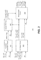
- FIG. 2 is a more detailed diagram of one embodiment of the PVVC engine of FIG. 1 .
- PVVC engine 140 includes transition detection circuit 141 , digital finite impulse response (FIR) filter 142 , FIR delay circuit 143 , and synchronizer circuit 144 , which are coupled as shown in FIG. 2 .
- FIR digital finite impulse response
- transition detection circuit 141 receives the incoming data signal Vip_out/Vin_out and the clock signal clk and determines whether the data signal meets a predetermined pattern. It is to be noted that Vip_out is the same as the serialized input data and Vin_out is its complement. If the data meets a predetermined pattern, then transition detection circuit 141 asserts a detect_flag signal, which is sent to digital FIR filter 142 .
- the predetermined pattern is a 0 bit followed by two consecutive 1 bits. In such a case, there is a two-clock-cycle delay between the incoming data and the detect_flag signal. It is to be noted that this delay depends on the specific implementation of transition detection circuit 141 and the length of the predetermined data pattern to be detected.
- transition detection circuit 141 is programmable to detect different predetermined data patterns. More specifically, in one embodiment, transition detection circuit 141 is programmable in user mode to detect different predetermined data patterns.
- the predetermined data pattern is a data transition (i.e., a 0 followed by a 1 or a 1 followed by a 0).
- FIR delay circuit 143 receives the clock signal clk and the data signals Vip_out/Vin_out and Vip_po 1 _out/Vin_po 1 _out. It is to be noted that Vip_po 1 _out/Vin_po 1 _out are delayed by one clock cycle relative to Vip_out/Vin_out. FIR delay circuit 143 then adds a two-clock-cycle latency to each of Vip_out/Vin_out and Vip_po 1 _out/Vin_po 1 _out, and outputs Vip_out 2 /Vin_out 2 and Vip_po 1 _out 2 /Vin_po 1 _out 2 .
- Vip_out 2 /Vin_out 2 and Vip_po 1 _out 2 /Vin_po 1 _out 2 are delayed versions, by two clock cycles, of Vip_out/Vin_out and Vip_po 1 _out/Vin_po 1 _out, respectively.
- the delay produced by FIR delay circuit 143 matches the delay of transition detection circuit 141 . It is to be noted that the delay produced by FIR delay circuit 143 is programmable. More specifically, the delay produced by FIR delay circuit 143 is programmable in user mode. For example, in another embodiment, where transition detection circuit 141 produces another delay, e.g., 3 clock cycles, then FIR delay circuit 143 is programmed to produce a 3 clock cycle delay between its input and output signals.
- Digital FIR filter 142 receives detect_flag from transition detection circuit 141 , Vip_po 1 _out 2 /Vin_po 1 _out 2 from FIR delay circuit 143 , and the clock signal clk.
- digital FIR filter 142 may include the functionality of transition detection circuit 141 , FIR delay circuit 143 , or both transition detection circuit 141 and FIR delay circuit 143 .
- the detect_flag is asserted for one bit, more specifically for the bit where the data transition occurs. For example, where a data transition occurs from 0 to 1, then the detect_flag is asserted during the 1 bit.
- digital FIR filter 142 provides a boost for the unit interval of the data bit, where the unit interval is the duration of the data bit.
- the response of digital FIR filter 142 is programmable. More specifically, it is programmable in user mode. Among other things, the programmability of the response allows digital FIR filter 142 to serve its function across various data rates.
- Synchronizer 144 receives Vip_po 2 _out 2 /Vin_po 2 _out 2 from digital FIR filter 142 , Vip_po 1 _out 2 /Vin_po 1 _out 2 and Vip_out 2 /Vin_out 2 from FIR delay circuit 143 , and the clock signal clk. Synchronizer 144 adds a two-clock-cycle delay to Vip_po 1 _out 2 /Vin_po 1 _out 2 and Vip_out 2 /Vin_out 2 to synchronize them to Vip_po 2 _out 2 /Vin_po 2 _out 2 .
- Vip_po 1 /Vin_po 1 , and Vip_po 2 /Vin_po 2 output by synchronizer 144 Vip_po 1 /Vin_po 1 , and Vip_po 2 /Vin_po 2 are synchronized (i.e., latency matched) with respect to Vip/Vin.
- the data Vip/Vin, Vip_po 1 /Vin_po 1 , and Vip_po 2 /Vin_po 2 (which may also herein be referred to as control signals) are respectively sent to drivers 110 , 120 , and 130 .
- Vip/Vin, Vip_po 1 /Vin_po 1 , and Vip_po 2 /Vin_po 2 are delayed (either as a result of an intentional delay added by synchronizer 144 for purposes of latency matching and/or as a result of inherent delays due to processing by synchronize 144 ) versions of Vip_out 2 /Vin_out 2 , Vip_po 1 _out 2 /Vin_po 1 _out 2 , and Vip_po 2 _out 2 /Vin_po 2 _out 2 , respectively.
- Compensation driver 130 adjusts the overall output voltage Vop and Von of the drivers so as to compensate for data dependent voltage variations.
- the orientation of the input signals determine the polarity of the mixing used for calculating the values of Vop and Von. More specifically, Vip and Vip_po 2 have the same orientation whereas Vip_po 1 has an opposite orientation form that of both Vip and Vip_po 2 . Similarly, Vin and Vin_po 2 have the same orientation whereas Vin_po 1 has an opposite orientation form that of both Vip and Vip_po 2 .
- PVVCE 140 When PVVCE 140 detects a predetermined data pattern, it provides control signals to compensation driver 130 to adjust the output voltages Vop and Von. More specifically, PVVCE 140 provides control signals to switches 133 to 136 of compensation driver 130 which results in adjusting the output voltages Vop and Von.
- Vip_po 2 when PVVCE 140 (by way of FIR filter 142 ) provides boost using the compensation driver 130 , Vip_po 2 has a binary value of 1, whereas Vin_po 2 has a binary value of 0. This results in a positive polarity on output Vop and a negative polarity on output Von. Conversely, in the non-boost condition, Vip_po 2 has a binary value of 0, whereas Vin_po 2 has a binary value of 1.
- the adjustments in the output voltages Vop and Von result in boosting the current at (i.e., providing additional current to) the parasitic capacitive nodes (e.g., nodes 165 and 175 ).
- the current boost provided by compensation driver 130 decreases the settling time needed to charge or discharge the parasitic capacitive nodes.
- the parasitic capacitive nodes charge or discharge within a unit interval which results in the removal of data dependent voltage variations when the pre-emphasis filter is enabled (i.e., when pre-emphasis driver 120 is enabled).
- the additional boost from compensation driver 130 decreases the settling time needed to charge or discharge the parasitic capacitive nodes without sacrificing performance (e.g., data speed) or flexibility (e.g., programmability) of the transmitter.
- PVVCE 140 in addition to detecting a predetermined data pattern, PVVCE 140 also evaluates the density of transitions and adjusts the current of current sources 131 and 132 accordingly. In one embodiment, the density of transitions is evaluated by transition detection circuit 141 . Thereafter, transition detection circuit 141 may provide control signals to current sources 131 and 132 of compensation driver 130 to increase their current. In one embodiment, transition detection circuit 141 may provide these control signals to current sources 131 and 132 via TDPTP controller 150 .
- FIG. 3 illustrates an exemplary data processing system including an exemplary PLD in which an embodiment of a pre-emphasis circuitry in accordance with the present invention might be implemented.
- Circuits including a pre-emphasis circuitry might be included in a variety of ICs, including ICs that are PLDs.
- PLDs also sometimes referred to as complex PLDs (CPLDs), programmable array logic (PALs), programmable logic arrays (PLAs), field PLAs (FPLAs), erasable PLDs (EPLDs), electrically erasable PLDs (EEPLDs), logic cell arrays (LCAs), field programmable gate arrays (FPGAs), or by other names
- PLDs also sometimes referred to as complex PLDs (CPLDs), programmable array logic (PALs), programmable logic arrays (PLAs), field PLAs (FPLAs), erasable PLDs (EPLDs), electrically erasable PLDs (EEPLDs), logic cell arrays (LCAs), field programmable gate arrays (FPGAs), or by other names
- CPLDs complex PLDs
- PALs programmable array logic
- ASICs Application specific integrated circuits
- PLD PLD
- Configuration elements may be realized as random access memory (RAM) bits, flip-flops, electronically erasable programmable read-only memory (EEPROM) cells, or other memory elements. Placing new data into the configuration elements programs or reprograms the PLD's logic functions and associated routing pathways. Configuration elements that are field programmable are often implemented as RAM cells (sometimes referred to a “configuration RAM” (CRAM)). However, many types of configurable elements may be used including static or dynamic RAM (SRAM or DRAM), electrically erasable read-only memory (EEROM), flash, fuse, and anti-fuse programmable connections. The programming of configuration elements could also be implemented through mask programming during fabrication of the device.
- RAM random access memory
- EEPROM electronically erasable programmable read-only memory
- configuration element will be used to refer to any programmable element that may be configured to determine functions implemented by other PLD elements.
- FIG. 3 illustrates, by way of example, PLD 310 in data processing system 300 .
- a pre-emphasis circuitry of this invention e.g., pre-emphasis circuitry 100
- PLDs such as PLD 310
- pre-emphasis circuitry 100 is on the same die/chip as PLD 310 .
- the logic for pre-emphasis circuitry 100 is supported by the programmable PLD core of PLD 310 .
- Data processing system 300 may include one or more of the following components: processor 340 , memory 350 , input/output (I/O) circuitry 320 , and peripheral devices 330 .
- I/O input/output
- a data processing system such as system 300 may include a single end-user system such as end-user system 370 or may include a plurality of systems working together as a data processing system.
- System 300 can be used in a wide variety of applications, such as computer networking, data networking, instrumentation, video processing, digital signal processing (DSP), or any other application where the advantage of using programmable or reprogrammable logic is desirable.
- PLD 310 can be used to perform a variety of different logic functions.
- PLD 310 can be configured as a processor or controller that works in cooperation with processor 340 (or, in alternative embodiments, a PLD might itself act as the sole system processor).
- PLD 310 may also be used as an arbiter for arbitrating access to a shared resource in system 300 .
- PLD 310 can be configured as an interface between processor 340 and one of the other components in system 300 . It should be noted that system 300 is only exemplary.
- system 300 is a digital system.
- a digital system is not intended to be limited to a purely digital system, but also encompasses hybrid systems that include both digital and analog subsystems.
- PVVC engine 140 is implemented in digital logic, it can easily be scaled and migrated to future process nodes.
Landscapes
- Engineering & Computer Science (AREA)
- Power Engineering (AREA)
- Computer Networks & Wireless Communication (AREA)
- Signal Processing (AREA)
- Physics & Mathematics (AREA)
- Computer Hardware Design (AREA)
- Computing Systems (AREA)
- General Engineering & Computer Science (AREA)
- Mathematical Physics (AREA)
- Logic Circuits (AREA)
Abstract
Description
Vip — po2_out2=(Vip — po1_out2) XOR (detect_flag)
Vin — po2_out2=(Vin — po1_out2) XOR (detect_flag),
where XOR represents the exclusive OR function. In other words, when detect_flag is asserted, the output (Vip_po2_out2/Vin_po2_out2) of
Vop=(Vip*Sa)−(Vip — po1*Sb)+(Vip — po2*Sc)
Von=(Vin*Sa)−(Vin — po1*Sb)+(Vin — po2*Sc),
where Sa, Sb, and Sc respectively represent the drive strength scaling factors for
Claims (21)
Priority Applications (1)
| Application Number | Priority Date | Filing Date | Title |
|---|---|---|---|
| US12/432,136 US9246715B1 (en) | 2009-04-29 | 2009-04-29 | Pre-emphasis circuitry including a pre-emphasis voltage variation compensation engine |
Applications Claiming Priority (1)
| Application Number | Priority Date | Filing Date | Title |
|---|---|---|---|
| US12/432,136 US9246715B1 (en) | 2009-04-29 | 2009-04-29 | Pre-emphasis circuitry including a pre-emphasis voltage variation compensation engine |
Publications (1)
| Publication Number | Publication Date |
|---|---|
| US9246715B1 true US9246715B1 (en) | 2016-01-26 |
Family
ID=55086285
Family Applications (1)
| Application Number | Title | Priority Date | Filing Date |
|---|---|---|---|
| US12/432,136 Active 2030-09-04 US9246715B1 (en) | 2009-04-29 | 2009-04-29 | Pre-emphasis circuitry including a pre-emphasis voltage variation compensation engine |
Country Status (1)
| Country | Link |
|---|---|
| US (1) | US9246715B1 (en) |
Cited By (2)
| Publication number | Priority date | Publication date | Assignee | Title |
|---|---|---|---|---|
| US20180083628A1 (en) * | 2016-09-22 | 2018-03-22 | Mediatek Singapore Pte. Ltd. | Signal processing devices and methods |
| US20180331585A1 (en) * | 2014-05-30 | 2018-11-15 | Sony Corporation | Transmission unit, reception unit, and communication system |
Citations (18)
| Publication number | Priority date | Publication date | Assignee | Title |
|---|---|---|---|---|
| US20040022311A1 (en) * | 2002-07-12 | 2004-02-05 | Zerbe Jared L. | Selectable-tap equalizer |
| US6956407B2 (en) * | 2003-11-04 | 2005-10-18 | Altera Corporation | Pre-emphasis circuitry and methods |
| US6977534B2 (en) * | 2002-12-23 | 2005-12-20 | Alcatel | Low voltage differential signaling [LVDS] driver with pre-emphasis |
| US20060034358A1 (en) * | 2004-08-16 | 2006-02-16 | Hitoshi Okamura | Methods and transmitters for loop-back adaptive pre-emphasis data transmission |
| US7034574B1 (en) * | 2004-08-17 | 2006-04-25 | Ami Semiconductor, Inc. | Low-voltage differential signal (LVDS) transmitter with high signal integrity |
| US20060158225A1 (en) * | 2003-12-17 | 2006-07-20 | Stojanovic Vladimir M | High speed signaling system with adaptive transmit pre-emphasis and reflection cancellation |
| US20060188043A1 (en) * | 2005-01-20 | 2006-08-24 | Zerbe Jared L | High-speed signaling systems with adaptable pre-emphasis and equalization |
| US20060280272A1 (en) * | 2003-04-09 | 2006-12-14 | Stojanovic Vladimir M | Data-level clock recovery |
| US20070002967A1 (en) * | 1997-06-20 | 2007-01-04 | Massachusetts Institute Of Technology | Digital transmitter |
| US7196557B1 (en) * | 2004-01-13 | 2007-03-27 | Altera Corporation | Multitap fractional baud period pre-emphasis for data transmission |
| US20070091993A1 (en) * | 2005-10-21 | 2007-04-26 | Zhiping Yang | Techniques for simulating a decision feedback equalizer circuit |
| US7227375B2 (en) * | 2003-09-11 | 2007-06-05 | Xilinx Inc. | DAC based driver with selectable pre-emphasis signal levels |
| US7256624B2 (en) * | 2003-10-28 | 2007-08-14 | Via Technologies, Inc. | Combined output driver |
| US7512193B1 (en) * | 2005-05-02 | 2009-03-31 | National Semiconductor Corporation | Circuit and method for pre-emphasis in data serialization |
| US7538588B2 (en) * | 2005-11-10 | 2009-05-26 | Via Technologies, Inc. | Dual-function drivers |
| US20090267640A1 (en) * | 2008-04-29 | 2009-10-29 | Qimonda Ag | System including preemphasis driver circuit and method |
| US7696787B2 (en) * | 2006-08-22 | 2010-04-13 | International Business Machines Corporation | Signal history controlled slew-rate transmission method and bus interface transmitter |
| US7848402B1 (en) * | 2005-09-29 | 2010-12-07 | Altera Corporation | Phase-adjusted pre-emphasis and equalization for data communication |
-
2009
- 2009-04-29 US US12/432,136 patent/US9246715B1/en active Active
Patent Citations (19)
| Publication number | Priority date | Publication date | Assignee | Title |
|---|---|---|---|---|
| US20070002967A1 (en) * | 1997-06-20 | 2007-01-04 | Massachusetts Institute Of Technology | Digital transmitter |
| US20090067484A1 (en) * | 2002-07-12 | 2009-03-12 | Rambus Inc. | Selectable-Tap Equalizer |
| US20040022311A1 (en) * | 2002-07-12 | 2004-02-05 | Zerbe Jared L. | Selectable-tap equalizer |
| US6977534B2 (en) * | 2002-12-23 | 2005-12-20 | Alcatel | Low voltage differential signaling [LVDS] driver with pre-emphasis |
| US20060280272A1 (en) * | 2003-04-09 | 2006-12-14 | Stojanovic Vladimir M | Data-level clock recovery |
| US7227375B2 (en) * | 2003-09-11 | 2007-06-05 | Xilinx Inc. | DAC based driver with selectable pre-emphasis signal levels |
| US7256624B2 (en) * | 2003-10-28 | 2007-08-14 | Via Technologies, Inc. | Combined output driver |
| US6956407B2 (en) * | 2003-11-04 | 2005-10-18 | Altera Corporation | Pre-emphasis circuitry and methods |
| US20060158225A1 (en) * | 2003-12-17 | 2006-07-20 | Stojanovic Vladimir M | High speed signaling system with adaptive transmit pre-emphasis and reflection cancellation |
| US7196557B1 (en) * | 2004-01-13 | 2007-03-27 | Altera Corporation | Multitap fractional baud period pre-emphasis for data transmission |
| US20060034358A1 (en) * | 2004-08-16 | 2006-02-16 | Hitoshi Okamura | Methods and transmitters for loop-back adaptive pre-emphasis data transmission |
| US7034574B1 (en) * | 2004-08-17 | 2006-04-25 | Ami Semiconductor, Inc. | Low-voltage differential signal (LVDS) transmitter with high signal integrity |
| US20060188043A1 (en) * | 2005-01-20 | 2006-08-24 | Zerbe Jared L | High-speed signaling systems with adaptable pre-emphasis and equalization |
| US7512193B1 (en) * | 2005-05-02 | 2009-03-31 | National Semiconductor Corporation | Circuit and method for pre-emphasis in data serialization |
| US7848402B1 (en) * | 2005-09-29 | 2010-12-07 | Altera Corporation | Phase-adjusted pre-emphasis and equalization for data communication |
| US20070091993A1 (en) * | 2005-10-21 | 2007-04-26 | Zhiping Yang | Techniques for simulating a decision feedback equalizer circuit |
| US7538588B2 (en) * | 2005-11-10 | 2009-05-26 | Via Technologies, Inc. | Dual-function drivers |
| US7696787B2 (en) * | 2006-08-22 | 2010-04-13 | International Business Machines Corporation | Signal history controlled slew-rate transmission method and bus interface transmitter |
| US20090267640A1 (en) * | 2008-04-29 | 2009-10-29 | Qimonda Ag | System including preemphasis driver circuit and method |
Cited By (3)
| Publication number | Priority date | Publication date | Assignee | Title |
|---|---|---|---|---|
| US20180331585A1 (en) * | 2014-05-30 | 2018-11-15 | Sony Corporation | Transmission unit, reception unit, and communication system |
| US10756579B2 (en) * | 2014-05-30 | 2020-08-25 | Sony Corporation | Transmission unit, reception unit, and communication system |
| US20180083628A1 (en) * | 2016-09-22 | 2018-03-22 | Mediatek Singapore Pte. Ltd. | Signal processing devices and methods |
Similar Documents
| Publication | Publication Date | Title |
|---|---|---|
| US6897699B1 (en) | Clock distribution network with process, supply-voltage, and temperature compensation | |
| US7528635B2 (en) | Multitap fractional baud period pre-emphasis for data transmission | |
| US8130016B2 (en) | Techniques for providing reduced duty cycle distortion | |
| US9048823B2 (en) | Duty cycle distortion correction circuitry | |
| US8416001B2 (en) | Techniques for reducing duty cycle distortion in periodic signals | |
| US9030244B1 (en) | Clock duty cycle calibration circuitry | |
| US20110279159A1 (en) | Circuits and methods for clock signal duty-cycle correction | |
| KR101043997B1 (en) | Low Voltage Digital Differential Signal Transmitter Circuit | |
| US8610462B1 (en) | Input-output circuit and method of improving input-output signals | |
| US10439615B2 (en) | Dynamic clock-data phase alignment in a source synchronous interface circuit | |
| US8390315B1 (en) | Configurable input-output (I/O) circuitry with pre-emphasis circuitry | |
| US7570094B2 (en) | Automatic duty cycle correction circuit with programmable duty cycle target | |
| CN1921318B (en) | Multi-channel high-speed transmitter circuit and receiver circuit | |
| US20180302073A1 (en) | Duty cycle calibration circuit and frequency synthesizer using the same | |
| US8159277B1 (en) | Techniques for providing multiple delay paths in a delay circuit | |
| US7626440B1 (en) | High speed level shift | |
| US9246715B1 (en) | Pre-emphasis circuitry including a pre-emphasis voltage variation compensation engine | |
| US9094239B1 (en) | Apparatus and method for polarity tap control | |
| US8729944B2 (en) | Clock generator with integrated phase offset programmability | |
| US7961000B1 (en) | Impedance matching circuit and method | |
| US8723575B1 (en) | Configurable delay circuitry with compensated delay | |
| US8816745B1 (en) | Equalizer circuitry including both inductor based and non-inductor based equalizer stages | |
| US8653853B1 (en) | Differential interfaces for power domain crossings | |
| JP4750842B2 (en) | Parameter control circuit | |
| US9479173B1 (en) | Transition accelerator circuitry |
Legal Events
| Date | Code | Title | Description |
|---|---|---|---|
| AS | Assignment |
Owner name: ALTERA CORPORATION, CALIFORNIA Free format text: ASSIGNMENT OF ASSIGNORS INTEREST;ASSIGNORS:CHAN, ALLEN;WONG, WILSON;HOANG, TIM TRI;REEL/FRAME:022613/0098 Effective date: 20090427 |
|
| STCF | Information on status: patent grant |
Free format text: PATENTED CASE |
|
| MAFP | Maintenance fee payment |
Free format text: PAYMENT OF MAINTENANCE FEE, 4TH YEAR, LARGE ENTITY (ORIGINAL EVENT CODE: M1551); ENTITY STATUS OF PATENT OWNER: LARGE ENTITY Year of fee payment: 4 |
|
| MAFP | Maintenance fee payment |
Free format text: PAYMENT OF MAINTENANCE FEE, 8TH YEAR, LARGE ENTITY (ORIGINAL EVENT CODE: M1552); ENTITY STATUS OF PATENT OWNER: LARGE ENTITY Year of fee payment: 8 |
|
| AS | Assignment |
Owner name: BARCLAYS BANK PLC, AS COLLATERAL AGENT, NEW JERSEY Free format text: SECURITY INTEREST;ASSIGNOR:ALTERA CORPORATION;REEL/FRAME:073431/0309 Effective date: 20250912 |