US9246034B2 - Solar cell and method of manufacturing the same - Google Patents
Solar cell and method of manufacturing the same Download PDFInfo
- Publication number
- US9246034B2 US9246034B2 US12/562,907 US56290709A US9246034B2 US 9246034 B2 US9246034 B2 US 9246034B2 US 56290709 A US56290709 A US 56290709A US 9246034 B2 US9246034 B2 US 9246034B2
- Authority
- US
- United States
- Prior art keywords
- semiconductor layer
- conductivity
- type
- type semiconductor
- amorphous semiconductor
- Prior art date
- Legal status (The legal status is an assumption and is not a legal conclusion. Google has not performed a legal analysis and makes no representation as to the accuracy of the status listed.)
- Expired - Fee Related, expires
Links
Images


Classifications
-
- H01L31/03529—
-
- H—ELECTRICITY
- H10—SEMICONDUCTOR DEVICES; ELECTRIC SOLID-STATE DEVICES NOT OTHERWISE PROVIDED FOR
- H10F—INORGANIC SEMICONDUCTOR DEVICES SENSITIVE TO INFRARED RADIATION, LIGHT, ELECTROMAGNETIC RADIATION OF SHORTER WAVELENGTH OR CORPUSCULAR RADIATION
- H10F77/00—Constructional details of devices covered by this subclass
- H10F77/10—Semiconductor bodies
- H10F77/14—Shape of semiconductor bodies; Shapes, relative sizes or dispositions of semiconductor regions within semiconductor bodies
- H10F77/148—Shapes of potential barriers
-
- H01L31/022425—
-
- H—ELECTRICITY
- H10—SEMICONDUCTOR DEVICES; ELECTRIC SOLID-STATE DEVICES NOT OTHERWISE PROVIDED FOR
- H10F—INORGANIC SEMICONDUCTOR DEVICES SENSITIVE TO INFRARED RADIATION, LIGHT, ELECTROMAGNETIC RADIATION OF SHORTER WAVELENGTH OR CORPUSCULAR RADIATION
- H10F77/00—Constructional details of devices covered by this subclass
- H10F77/20—Electrodes
- H10F77/206—Electrodes for devices having potential barriers
- H10F77/211—Electrodes for devices having potential barriers for photovoltaic cells
- H10F77/219—Arrangements for electrodes of back-contact photovoltaic cells
-
- Y—GENERAL TAGGING OF NEW TECHNOLOGICAL DEVELOPMENTS; GENERAL TAGGING OF CROSS-SECTIONAL TECHNOLOGIES SPANNING OVER SEVERAL SECTIONS OF THE IPC; TECHNICAL SUBJECTS COVERED BY FORMER USPC CROSS-REFERENCE ART COLLECTIONS [XRACs] AND DIGESTS
- Y02—TECHNOLOGIES OR APPLICATIONS FOR MITIGATION OR ADAPTATION AGAINST CLIMATE CHANGE
- Y02E—REDUCTION OF GREENHOUSE GAS [GHG] EMISSIONS, RELATED TO ENERGY GENERATION, TRANSMISSION OR DISTRIBUTION
- Y02E10/00—Energy generation through renewable energy sources
- Y02E10/50—Photovoltaic [PV] energy
Definitions
- the invention relates to aback junction solar cell and a method of manufacturing the solar cell.
- Solar cells are now expected to be a new energy source because of their capability to convert sunlight, which is clean and in unlimited supply, directly into electricity.
- the output of a single solar cell is only several watts. Accordingly, if solar cells are used as an electric-power source (energy source) for a house, building or the like, a solar cell module is used in which multiple solar cells are electrically connected together to increase the output.
- a so-called back junction solar cell in which, for the purpose of expanding the light-receiving area, multiple lines of n type regions and multiple lines of p type regions are formed alternately on a back surface of a semiconductor substrate.
- a collecting electrode including a transparent conductive layer and a conductive layer is formed on each n type semiconductor region. This collecting electrode collects carriers (electrons) from the n type semiconductor region.
- a collecting electrode including a transparent conductive layer and a conductive layer is formed on each p type region. This collecting electrode collects carriers (positive holes or acceptors) from the p type semiconductor region.
- each of the n type semiconductor region, the p type semiconductor region and the transparent conductive layer can be formed in a predetermined pattern by means of a metal mask (see, for example, Japanese Patent Application Publication No. 2005-101427).
- the use of metal masks has an advantage because high positional accuracy of the predetermined pattern can be achieved.
- the conductive layer can be formed by a printing method or a sputtering method.
- n type semiconductor regions and p type semiconductor regions are formed in the metal mask more densely.
- the metal mask with such a structure has a lower strength, and thus tends to have some portions broken or bent (raised). This may cause a problem of damaging the surface of the semiconductor substrate or misaligning the pattern. For this reason, there is a limitation to a microscopic formation of n type semiconductor regions and p type semiconductor regions by means of metal masks.
- the invention has been made in view of the above-described circumstances and aims to provide a solar cell in which n type semiconductor regions and p type semiconductor regions are densely, microscopically formed, and to provide a method of manufacturing the solar cell.
- a first aspect of the invention is a method of manufacturing a solar cell, including: a step A of forming a semiconductor layer of a first conductivity type extending along a predetermined direction on a back surface of a semiconductor substrate that includes a light-receiving surface and the back surface located on the opposite side to the light-receiving surface, the first-conductivity-type semiconductor layer being divided into plural island-shaped sections arranged side by side in the predetermined direction; a step B of forming a semiconductor layer of a second conductivity type in the predetermined direction on the back surface; and a step C of forming conductive layers respectively on the first-conductivity-type semiconductor layer and the second-conductivity-type semiconductor layer by using a conductive paste, the conductive layer to be formed on the first-conductivity-type semiconductor layer being formed by a printing method such that the conductive layer to be formed on the first-conductivity-type semiconductor layer extends along a line of the plural island-shaped sections to bridge adjacent two of the plural island-shaped sections.
- the first-conductivity-type semiconductor layer is formed as plural island-shaped sections arranged side by side in the predetermined direction. Even though a metal mask is used for forming the first-conductivity-type semiconductor layer, the first-conductivity-type semiconductor layer can have a thinner line width by using a metal mask. Further, according to the first aspect, since the conductive layer is formed by a printing method, the thinner lined conductive layer can be formed to bridge adjacent two of the plural island-shaped sections. A solar cell having high carrier-collection efficiency can thereby be manufactured.
- the first-conductivity-type semiconductor layer may be formed using a metal mask including: plural slits corresponding to the plural island-shaped sections; and a bridge portion between adjacent two of the slits.
- the semiconductor substrate may be made of a semiconductor substrate of the first conductivity type, and in step B, the second-conductivity-type semiconductor layer may be formed so as to have a width that is larger than the width of the first-conductivity-type semiconductor layer.
- a second aspect of the invention is a solar cell comprising: a semiconductor substrate including a light-receiving surface and a back surface located on the opposite side to the light-receiving surface; a semiconductor layer of a first conductivity type formed along a predetermined direction on the back surface, the first-conductivity-type semiconductor layer being formed as a plurality of island-shaped sections arranged in the predetermined direction; a semiconductor layer of a second conductivity type formed in the predetermined direction on the back surface; and conductive layers that are respectively formed on the first-conductivity-type semiconductor layer and the second-conductivity-type semiconductor layer, wherein the conductive layer on the first-conductivity-type semiconductor layer is made of a conductive paste such that the conductive layer on the first-conductive-type semiconductor layer extends along a line of the plural island-shaped sections to connect adjacent two of the plural island-shaped sections to each other.
- the semiconductor substrate may be made of a semiconductor of the first conductivity type, and the second-conductivity-type semiconductor layer may have a width that is larger than the width of the first-conductivity-type semiconductor layer.
- FIG. 1 is a plan view of aback surface of solar cell 100 according to an embodiment of the invention.
- FIG. 2 is an enlarged sectional view taken along line A-A of FIG. 1 .
- FIG. 3 is an enlarged sectional view taken along line B-B of FIG. 1 .
- FIG. 4 is a plan view of metal mask M 1 according to the embodiment.
- FIG. 5 is a diagram for describing a method of manufacturing solar cell 100 according to the embodiment.
- FIG. 6 is a plan view of metal mask M 2 according to the embodiment.
- FIG. 7 is a diagram for describing the method of manufacturing solar cell 100 according to the embodiment.
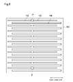
- FIG. 8 is a plan view of metal mask M 3 according to the embodiment.
- FIG. 9 is a diagram for describing the method of manufacturing solar cell 100 according to the embodiment.
- Prepositions such as “on”, “over” and “above” may be defined with respect to a surface, for example a layer surface, regardless of that surface's orientation in space.
- the preposition “above” may be used in the specification and claims even if a layer is in contact with another layer.
- the preposition “on” may be used in the specification and claims when a layer is not in contact with another layer, for example, when there is an intervening layer between them.
- FIG. 1 is a plan view of a back surface of solar cell 100 .
- FIG. 2 is an enlarged sectional view taken along line A-A of FIG. 1 .
- solar cell 100 includes n type semiconductor substrate 10 , i type amorphous semiconductor layer 11 , n type amorphous semiconductor layers 12 n , p type amorphous semiconductor layers 12 p , n side collecting electrodes 13 n and p side collecting electrodes 13 p.
- N type semiconductor substrate 10 includes a light-receiving surface that receives light and aback surface provided on the opposite side of n type semiconductor substrate 10 to the light-receiving surface.
- N type semiconductor substrate 10 is made of a semiconductor material doped with an n type dopant. Some examples of the semiconductor material are such crystalline semiconductor materials as single-crystal Si and poly-crystal Si, and such compound semiconductor materials as GaAs and InP. That is, an ordinary semiconductor material can be used for the purpose.
- n type semiconductor substrate 10 Upon receiving light, n type semiconductor substrate 10 generates carriers (acceptors and electrons). Since the conductivity type of n type semiconductor substrate 10 is n type, the electrons of the two different kinds of photogenerated carriers are the majority carriers whereas the acceptors are the minority carriers.
- I type amorphous semiconductor layer 11 is formed so as to cover substantially the entire back surface of n type semiconductor substrate 10 .
- I type amorphous semiconductor layer 11 is an intrinsic amorphous semiconductor layer that is formed either without any dopant added to or with a small amount of dopant added to.
- I type amorphous semiconductor layer 11 contains hydrogen within its film, and thus has a passivation effect of preventing the recombination of photogenerated carriers in the back surface of n type semiconductor substrate 10 .
- Each of n type amorphous semiconductor layers 12 n is formed on i type amorphous semiconductor layer 11 and extends in a first direction.
- the electrons, which are the majority carriers, are collected from n type semiconductor substrate 10 to n type amorphous semiconductor layers 12 n.
- each n type amorphous semiconductor layer 12 n is formed of two island-shaped n type amorphous semiconductor layer sections 12 n 1 .
- Two island-shaped n type amorphous semiconductor layer sections 12 n 1 are arranged side by side in a line in the first direction.
- FIG. 3 is an enlarged view taken along line B-B of FIG. 1 .
- two island-shaped n type amorphous semiconductor layer sections 12 n 1 are separated away from each other by distance Ln 1 at the center of n type semiconductor substrate 10 in the first direction.
- each of p type amorphous semiconductor layers 12 p is formed on i type amorphous semiconductor layer 11 and extends in the first direction.
- the acceptors which are the minority carriers, are collected from n type semiconductor substrate 10 to p type amorphous semiconductor layers 12 p.
- n type amorphous semiconductor layers 12 n and p type amorphous semiconductor layers 12 p are arranged alternately in a second direction that is substantially orthogonal to the first direction.
- each n type amorphous semiconductor layer 12 n has line width Ln that is smaller than line width Lp of each p type amorphous semiconductor layer 12 p .
- N type amorphous semiconductor layers 12 n collect the electrons, which are the majority carriers of n type semiconductor substrate 10 . Accordingly, even if the line width of each n type amorphous semiconductor layer 12 n is narrowed, the collection efficiency is not lowered.
- p type amorphous semiconductor layers 12 p collect the acceptors, which are minority carriers of n type semiconductor substrate 10 . Accordingly, if the line width of each p type amorphous semiconductor layer 12 p is widened, the collection efficiency can be improved.
- N side collecting electrodes 13 n are collecting electrodes to collect electrons from n type semiconductor substrate 10 .
- each n side collecting electrode 13 n is formed in the first direction.
- Each n side collecting electrode 13 n is formed on and between two island-shaped n type amorphous semiconductor layer sections 12 n 1 . That is, each n side collecting electrode 13 n extends on a line of plural island-shaped n type amorphous semiconductor layer sections 12 n 1 to bridge the plural sections 12 n 1
- each n side collecting electrode 13 n is formed of n side transparent conductive layer 13 n 1 and n side conductive layer 13 n 2 .
- N side transparent conductive layer 13 n 1 is formed on two island-shaped n type amorphous semiconductor layer sections 12 n 1 .
- N side conductive layer 13 n 2 is formed on corresponding n side transparent conductive layer 13 n 1 and formed on i type amorphous semiconductor layer 11 between two island-shaped n type amorphous semiconductor layer sections 12 n 1 , as shown in FIG. 3 .
- N side transparent conductive layers 13 n 1 are made of an oxide of In, Zn, Sn, Ti, W, or the like.
- N side conductive layers 13 n 2 are made of a thermosetting-resin paste including a thermosetting resin and multiple conductive fillers. An example of such conductive fillers is silver particles.
- P side collecting electrodes 13 p are collecting electrode to collect acceptors from n type semiconductor substrate 10 .
- each p side collecting electrode 13 p is formed on corresponding p type amorphous semiconductor layer 12 p in the first direction.
- each p side collecting electrode 13 p is formed of p side transparent conductive layer 13 p 1 and p side conductive layer 13 p 2 .
- P side transparent conductive layer 13 p 1 is formed on p type amorphous semiconductor layer 12 p .
- P side conductive layer 13 p 2 is formed on p side transparent conductive layer 13 p 1 .
- P side transparent conductive layers 13 p 1 are made of an oxide of In, Zn, Sn, Ti, W, or the like.
- P side conductive layers 13 p 2 are made of a thermosetting-resin paste including a thermosetting resin and multiple conductive fillers.
- i type amorphous semiconductor layer 11 is formed substantially on the entire back surface of n type semiconductor substrate 10 by a CVD method.
- FIG. 4 is a plan view of metal mask M 1 .
- metal mask M 1 includes multiple slits H 1 corresponding to the forming pattern of multiple island-shaped n type amorphous semiconductor layer sections 12 n 1 . That is, metal mask M 1 has bridge portions P each of which is formed between two corresponding slits H 1 arranged side by side in the first direction. Bridge portions P have a function of reinforcing the overall strength of metal mask M 1 .
- Each of slits H 1 has width (line width) Ln (see FIG.
- n type amorphous semiconductor layers 12 n each formed of two island-shaped n type amorphous semiconductor layer section 12 n 1 that are arranged side by side in the first direction, are formed.
- FIG. 6 is a plan view of metal mask M 2 .
- metal mask M 2 is formed with multiple slits H 2 corresponding to the forming pattern of multiple p type amorphous semiconductor layers 12 p .
- Each of multiple slits H 2 has width (line width) Lp (see FIG. 2 ).
- FIG. 7 shows, p type amorphous semiconductor layers 12 p are formed in the first direction using metal mask M 2 .
- FIG. 8 is a plan view of metal mask M 3 .
- metal mask M 3 is formed with multiple slits H 3 corresponding to the forming pattern of multiple island-shaped n type amorphous semiconductor layer sections 12 n 1 and multiple slits H 4 corresponding to the forming pattern of multiple p type amorphous semiconductor layers 12 p .
- each slit H 3 are preferably smaller than the dimensions of each slit H 1 .
- the dimensions of each slit H 4 are preferably smaller than the dimensions of each slit H 2 .
- metal mask M 3 includes bridge portions P each of which is formed between two corresponding slits H 3 arranged side by side in the first direction. Bridge portions P have a function of reinforcing the overall strength of metal mask M 3 .
- FIG. 9 shows, n side transparent conductive layers 13 n 1 and p side transparent conductive layers 13 p 1 are formed in the first direction using metal mask M 3 .
- thermosetting-resin paste is placed both on n side transparent conductive layers 13 n 1 and on p side transparent conductive layers 13 p 1 and also is placed at every interstice between two n side transparent conductive layers 13 n 1 arranged side by side in the first direction (see FIG. 3 ), by a printing method such as a screen printing method.
- a printing method such as a screen printing method.
- n side conductive layers 13 n 2 and p side conductive layers 13 p 2 are formed.
- two island-shaped n type amorphous semiconductor layer sections 12 n 1 are electrically connected to each other via their respective two n side transparent conductive layer 13 n 1 by n side conductive layer 13 n 2 (see FIGS. 1 and 3 ).
- thermosetting-resin paste is heated at a temperature of 300° C. or lower.
- This operation evaporates the organic solvent contained in the thermosetting-resin paste and hardens the thermosetting-resin paste.
- the thermosetting-resin paste is heated at a temperature of 300° C. or lower, and thus the conductive fillers are not alloyed. Accordingly, the thermosetting-resin paste and i type amorphous semiconductor layer 11 are electrically isolated from each other. Consequently, no leakage current occurs between n side conductive layers 13 n 2 and n type semiconductor substrate 10 as well as between p side conductive layers 13 p 2 and n type semiconductor substrate 10 .
- metal mask M 1 is formed with: pairs of slits H 1 corresponding to the forming pattern of pairs of island-shaped n type amorphous semiconductor layer sections 12 n 1 ; and bridge portions P each of which is formed between corresponding pair of slits H 1 .
- This configuration allows a distance between slits H 1 to be narrowed, while maintaining the strength of metal mask M 1 . That is, more densely, microscopically formed n type amorphous semiconductor layers 12 n can be provided, while preventing the damages on the substrate and the misalignment of the pattern.
- n side conductive layers 13 n 2 are formed by a printing method. Accordingly, n side conductive layers 13 n 2 each having a smaller line width can be formed on and between corresponding pair of island-shaped n type amorphous semiconductor layer sections 12 n 1 . This configuration can provide a solar cell of high conversion efficiency.
- metal mask M 3 is formed with: pairs of slits H 3 corresponding to the forming pattern of pairs of island-shaped n type amorphous semiconductor layer sections 12 n 1 ; and bridge portions P each of which is formed between corresponding pair of slits H 3 . Accordingly, this configuration allows the widths (line widths) of each of slits H 3 and slit H 4 to be narrowed and the distance between each slit H 3 and adjacent slit H 4 to be narrowed, while maintaining the strength of metal mask M 3 . As a result, while preventing the damages on the substrate and the misalignment of the pattern, more densely, microscopically formed n side transparent conductive layers 13 n 1 and p side transparent conductive layers 13 p 1 can be provided.
- n side conductive layers 13 n 2 are made of a thermosetting-resin paste that can be hardened at a relatively low temperature. Accordingly, even through each n side conductive layer 13 n 2 is in direct contact with i type amorphous semiconductor layer 11 at the interstice between the pair of n side transparent conductive layer sections 13 n 1 that are formed correspondingly to the pair of slits H 3 , the resistivity of i type amorphous semiconductor layer 11 is not lowered, and thus, no leakage current occurs between n side conductive layers 13 n 2 and n type semiconductor substrate 10 .
- line width Lp of each p type amorphous semiconductor layer 12 p is larger than line width Ln of each n type amorphous semiconductor layer 12 n . Accordingly, the acceptors, which are the minority carriers of all the carriers generated by n type semiconductor substrate 10 , can be efficiently collected to p type amorphous semiconductor layers 12 p . This can provide the carrier-collection efficiency of entire solar cell 100 .
- n type amorphous semiconductor layers 12 n and p type amorphous semiconductor layers 12 p are formed on the back surface of n type semiconductor substrate 10 by the CVD method.
- n type semiconductor layers and p type semiconductor layers may be formed on the back surface of n type semiconductor substrate 10 by a thermal diffusion method.
- the n type amorphous semiconductor layers and the n side collecting electrodes may be formed sequentially in the second direction, and, on the other side, in the first direction, of the back surface of solar cell 100 , the p type amorphous semiconductor layers and the p side collecting electrodes may be formed sequentially in the second direction. Accordingly, the carriers can be collected from the entire back surface of solar cell 100 . Consequently, the carrier-collection efficiency can be further improved.
- each n type amorphous semiconductor layer 12 n is formed of two island-shaped n type amorphous semiconductor layer sections 12 n 1 , but this is not the only possible example.
- each n type amorphous semiconductor layer 12 n may be formed of three or more island-shaped n type amorphous semiconductor layer sections 12 n 1 .
- the metal mask M 3 has more bridge portions P. Accordingly, the strength of metal mask M 3 can be enhanced furthermore.
- each n type amorphous semiconductor layer 12 n is formed of plural island-shaped n type amorphous semiconductor layer sections 12 n 1 .
- each p type amorphous semiconductor layer 12 p may be formed of plural island-shaped p type amorphous semiconductor layer sections.
- each slit H 2 extending along the first direction is divided by at least one bridge portion into plural slits H 2 in metal mask M 1
- each slit H 4 extending along the first direction is divided by at least one bridge portion into plural slits H 4 in metal mask M 3 .
- metal mask M 1 includes the divided slits H 2
- a distance between slits H 2 can be narrowed, while maintaining the strength of metal mask M 1
- metal mask M 3 includes the divided slits H 4
- a distance between slits H 4 , a distance between slits H 4 and a distance between slits H 3 and H 4 can be narrowed, while maintaining the strength of metal mask M 3 .
- each p side conductive layer 13 p 2 is indirect contact with i type amorphous semiconductor layer 11 , the resistivity of i type amorphous semiconductor layer 11 is not lowered, and thus, no leakage current occurs between p side conductive layers 13 p 2 and i type amorphous semiconductor layer 11 .
- n side conductive layers 13 n 2 and p side conductive layer 13 p 2 are formed by placing a thermosetting-resin paste by the printing method, but this is not the only possible example.
- n side conductive layers 13 n 2 and p side conductive layer 13 p 2 only have to be formed by a method that does not use any metal mask.
- N side conductive layers 13 n 2 and p side conductive layer 13 p 2 may be formed by other kinds of conductive paste than the thermosetting-resin paste.
- i type amorphous semiconductor layer 11 is formed substantially on the entire back surface of solar cell 100 , but i type amorphous semiconductor layer 11 does not have to be formed. Even in this case, the thermosetting-resin paste is not alloyed, so that no leakage current occurs between n side conductive layers 13 n 2 and n type semiconductor substrate 10 .
- the term “amorphous” also refers to the material contains microscopic crystal particles, and the term “semiconductor” includes common fact that the semiconductors such as silicon, silicon carbide, or the like.
Landscapes
- Photovoltaic Devices (AREA)
- Life Sciences & Earth Sciences (AREA)
- Engineering & Computer Science (AREA)
- Sustainable Development (AREA)
- Sustainable Energy (AREA)
Abstract
Description
Claims (3)
Applications Claiming Priority (2)
| Application Number | Priority Date | Filing Date | Title |
|---|---|---|---|
| JP2008-250737 | 2008-09-29 | ||
| JP2008250737A JP5261110B2 (en) | 2008-09-29 | 2008-09-29 | Solar cell manufacturing method and solar cell |
Publications (2)
| Publication Number | Publication Date |
|---|---|
| US20100078069A1 US20100078069A1 (en) | 2010-04-01 |
| US9246034B2 true US9246034B2 (en) | 2016-01-26 |
Family
ID=42056091
Family Applications (1)
| Application Number | Title | Priority Date | Filing Date |
|---|---|---|---|
| US12/562,907 Expired - Fee Related US9246034B2 (en) | 2008-09-29 | 2009-09-18 | Solar cell and method of manufacturing the same |
Country Status (2)
| Country | Link |
|---|---|
| US (1) | US9246034B2 (en) |
| JP (1) | JP5261110B2 (en) |
Cited By (2)
| Publication number | Priority date | Publication date | Assignee | Title |
|---|---|---|---|---|
| USD785559S1 (en) * | 2015-08-19 | 2017-05-02 | Shin-Etsu Chemical Co., Ltd. | Solar cell |
| USD786189S1 (en) * | 2015-08-19 | 2017-05-09 | Shin-Etsu Chemical Co., Ltd. | Solar cell |
Families Citing this family (12)
| Publication number | Priority date | Publication date | Assignee | Title |
|---|---|---|---|---|
| WO2011149021A1 (en) * | 2010-05-28 | 2011-12-01 | 株式会社エバテック | Method for manufacturing photovoltaic element, and photovoltaic element |
| JP5974300B2 (en) * | 2010-08-24 | 2016-08-23 | パナソニックIpマネジメント株式会社 | Solar cell and manufacturing method thereof |
| WO2012132834A1 (en) * | 2011-03-28 | 2012-10-04 | 三洋電機株式会社 | Solar cell and method for producing solar cell |
| GB2491209B (en) * | 2011-05-27 | 2013-08-21 | Renewable Energy Corp Asa | Solar cell and method for producing same |
| KR101948206B1 (en) | 2012-03-02 | 2019-02-14 | 인텔렉츄얼 키스톤 테크놀로지 엘엘씨 | thin film type solar cell and the fabrication method thereof |
| JP5774204B2 (en) * | 2012-03-29 | 2015-09-09 | 三菱電機株式会社 | Photovoltaic element, manufacturing method thereof, and solar cell module |
| WO2016147924A1 (en) | 2015-03-13 | 2016-09-22 | シャープ株式会社 | Photoelectric conversion element and photoelectric conversion module |
| CN105097068B (en) * | 2015-06-25 | 2017-03-08 | 英利能源(中国)有限公司 | Conductive adhesive, solar battery string and preparation method thereof |
| US10505064B2 (en) | 2015-09-14 | 2019-12-10 | Sharp Kabushiki Kaisha | Photovoltaic device |
| JP6639295B2 (en) * | 2016-03-23 | 2020-02-05 | シャープ株式会社 | Photoelectric conversion device, photoelectric conversion module and photovoltaic power generation system |
| US10141462B2 (en) | 2016-12-19 | 2018-11-27 | Sunpower Corporation | Solar cells having differentiated P-type and N-type architectures |
| JP7323107B2 (en) * | 2018-03-26 | 2023-08-08 | シャープ株式会社 | Photoelectric conversion element |
Citations (13)
| Publication number | Priority date | Publication date | Assignee | Title |
|---|---|---|---|---|
| US4065781A (en) * | 1974-06-21 | 1977-12-27 | Westinghouse Electric Corporation | Insulated-gate thin film transistor with low leakage current |
| JPS63287077A (en) | 1987-05-20 | 1988-11-24 | Hitachi Ltd | Photoelectric conversion device |
| US5331183A (en) * | 1992-08-17 | 1994-07-19 | The Regents Of The University Of California | Conjugated polymer - acceptor heterojunctions; diodes, photodiodes, and photovoltaic cells |
| US5428249A (en) * | 1992-07-15 | 1995-06-27 | Canon Kabushiki Kaisha | Photovoltaic device with improved collector electrode |
| US20040043528A1 (en) * | 2000-09-13 | 2004-03-04 | Wolfgang Kruhler | Photovoltaic component and module |
| US20050018975A1 (en) * | 2003-07-23 | 2005-01-27 | Yen-Ping Ho | Metallized optical fibers and ferrules for optical fibers for direct attachment to photodiodes |
| US20050023974A1 (en) * | 2003-08-01 | 2005-02-03 | Universal Display Corporation | Protected organic electronic devices and methods for making the same |
| JP2005101427A (en) | 2003-09-26 | 2005-04-14 | Sanyo Electric Co Ltd | Photovoltaic element and manufacturing method thereof |
| US20060162770A1 (en) * | 2002-10-03 | 2006-07-27 | Fujikura Ltd | Electrode substrate, photoelectric conversion element, conductive glass substrate and production method therefo, and pigment sensitizing solar cell |
| JP2006303322A (en) | 2005-04-22 | 2006-11-02 | Sharp Corp | Solar cell |
| US20070144577A1 (en) * | 2005-12-23 | 2007-06-28 | Rubin George L | Solar cell with physically separated distributed electrical contacts |
| US20070151599A1 (en) * | 2005-12-30 | 2007-07-05 | Sunpower Corporation | Solar cell having polymer heterojunction contacts |
| WO2008125446A2 (en) * | 2007-03-28 | 2008-10-23 | Commissariat A L'energie Atomique | Photovoltaic device with discontinuous interdigited heterojunction structure |
Family Cites Families (2)
| Publication number | Priority date | Publication date | Assignee | Title |
|---|---|---|---|---|
| JPS62276504A (en) * | 1986-05-23 | 1987-12-01 | Citizen Watch Co Ltd | Mask for dyeing color filter |
| JP2006341547A (en) * | 2005-06-10 | 2006-12-21 | Sharp Corp | Mask for printing, screen printing method, method for producing photoelectric conversion element, and photoelectric conversion element |
-
2008
- 2008-09-29 JP JP2008250737A patent/JP5261110B2/en not_active Expired - Fee Related
-
2009
- 2009-09-18 US US12/562,907 patent/US9246034B2/en not_active Expired - Fee Related
Patent Citations (14)
| Publication number | Priority date | Publication date | Assignee | Title |
|---|---|---|---|---|
| US4065781A (en) * | 1974-06-21 | 1977-12-27 | Westinghouse Electric Corporation | Insulated-gate thin film transistor with low leakage current |
| JPS63287077A (en) | 1987-05-20 | 1988-11-24 | Hitachi Ltd | Photoelectric conversion device |
| US5428249A (en) * | 1992-07-15 | 1995-06-27 | Canon Kabushiki Kaisha | Photovoltaic device with improved collector electrode |
| US5331183A (en) * | 1992-08-17 | 1994-07-19 | The Regents Of The University Of California | Conjugated polymer - acceptor heterojunctions; diodes, photodiodes, and photovoltaic cells |
| US20040043528A1 (en) * | 2000-09-13 | 2004-03-04 | Wolfgang Kruhler | Photovoltaic component and module |
| US20060162770A1 (en) * | 2002-10-03 | 2006-07-27 | Fujikura Ltd | Electrode substrate, photoelectric conversion element, conductive glass substrate and production method therefo, and pigment sensitizing solar cell |
| US20050018975A1 (en) * | 2003-07-23 | 2005-01-27 | Yen-Ping Ho | Metallized optical fibers and ferrules for optical fibers for direct attachment to photodiodes |
| US20050023974A1 (en) * | 2003-08-01 | 2005-02-03 | Universal Display Corporation | Protected organic electronic devices and methods for making the same |
| JP2005101427A (en) | 2003-09-26 | 2005-04-14 | Sanyo Electric Co Ltd | Photovoltaic element and manufacturing method thereof |
| JP2006303322A (en) | 2005-04-22 | 2006-11-02 | Sharp Corp | Solar cell |
| US20070144577A1 (en) * | 2005-12-23 | 2007-06-28 | Rubin George L | Solar cell with physically separated distributed electrical contacts |
| US20070151599A1 (en) * | 2005-12-30 | 2007-07-05 | Sunpower Corporation | Solar cell having polymer heterojunction contacts |
| WO2008125446A2 (en) * | 2007-03-28 | 2008-10-23 | Commissariat A L'energie Atomique | Photovoltaic device with discontinuous interdigited heterojunction structure |
| US20100032014A1 (en) * | 2007-03-28 | 2010-02-11 | Commissariat A L'energie Atomique | Photovoltaic device with a discontinuous interdigitated heterojunction structure |
Cited By (2)
| Publication number | Priority date | Publication date | Assignee | Title |
|---|---|---|---|---|
| USD785559S1 (en) * | 2015-08-19 | 2017-05-02 | Shin-Etsu Chemical Co., Ltd. | Solar cell |
| USD786189S1 (en) * | 2015-08-19 | 2017-05-09 | Shin-Etsu Chemical Co., Ltd. | Solar cell |
Also Published As
| Publication number | Publication date |
|---|---|
| US20100078069A1 (en) | 2010-04-01 |
| JP2010080888A (en) | 2010-04-08 |
| JP5261110B2 (en) | 2013-08-14 |
Similar Documents
| Publication | Publication Date | Title |
|---|---|---|
| US9246034B2 (en) | Solar cell and method of manufacturing the same | |
| USRE46515E1 (en) | Solar cell | |
| US8053666B2 (en) | Solar cell and manufacturing method of the solar cell | |
| US20110041908A1 (en) | Rear-contact solar cell having elongate, inter-digitated emitter and base regions on the rear side and method for producing the same | |
| JP6360471B2 (en) | Photoelectric conversion element, photoelectric conversion module, and photovoltaic power generation system | |
| EP2797119B1 (en) | Solar cell | |
| US20100288346A1 (en) | Configurations and methods to manufacture solar cell device with larger capture cross section and higher optical utilization efficiency | |
| KR102586115B1 (en) | Bifacial silicon solar cell | |
| JP2024049279A (en) | Solar Cells and Photovoltaic Modules | |
| US20240413259A1 (en) | Solar cell, photovoltaic module, and photovoltaic system | |
| US9761743B2 (en) | Photoelectric conversion element | |
| WO2014157525A1 (en) | Photoelectric conversion element | |
| JP2010283406A (en) | Solar cell | |
| CN103943710B (en) | Solar cell and its manufacture method | |
| KR101180813B1 (en) | Solar cell | |
| US9780241B2 (en) | Solar cell | |
| KR20100064478A (en) | Solar cell | |
| KR101975580B1 (en) | Solar cell | |
| US9627557B2 (en) | Solar cell | |
| CN113826214B (en) | Crystalline silicon solar cells | |
| US20130160853A1 (en) | Solar cell having a pn hetero-junction | |
| CN222088623U (en) | Solar cells and photovoltaic modules | |
| CN223334974U (en) | Back contact battery and photovoltaic module | |
| CN223053382U (en) | Back contact solar cells and photovoltaic modules | |
| KR102451084B1 (en) | High efficiency solar cell module |
Legal Events
| Date | Code | Title | Description |
|---|---|---|---|
| AS | Assignment |
Owner name: SANYO ELECTRIC CO., LTD.,JAPAN Free format text: ASSIGNMENT OF ASSIGNORS INTEREST;ASSIGNOR:IDE, DAISUKE;REEL/FRAME:023255/0743 Effective date: 20090910 Owner name: SANYO ELECTRIC CO., LTD., JAPAN Free format text: ASSIGNMENT OF ASSIGNORS INTEREST;ASSIGNOR:IDE, DAISUKE;REEL/FRAME:023255/0743 Effective date: 20090910 |
|
| AS | Assignment |
Owner name: PANASONIC CORPORATION, JAPAN Free format text: ASSIGNMENT OF ASSIGNORS INTEREST;ASSIGNOR:SANYO ELECTRIC CO., LTD.;REEL/FRAME:035071/0276 Effective date: 20150130 Owner name: PANASONIC INTELLECTUAL PROPERTY MANAGEMENT CO., LT Free format text: ASSIGNMENT OF ASSIGNORS INTEREST;ASSIGNOR:PANASONIC CORPORATION;REEL/FRAME:035071/0508 Effective date: 20150130 |
|
| ZAAA | Notice of allowance and fees due |
Free format text: ORIGINAL CODE: NOA |
|
| ZAAB | Notice of allowance mailed |
Free format text: ORIGINAL CODE: MN/=. |
|
| STCF | Information on status: patent grant |
Free format text: PATENTED CASE |
|
| MAFP | Maintenance fee payment |
Free format text: PAYMENT OF MAINTENANCE FEE, 4TH YEAR, LARGE ENTITY (ORIGINAL EVENT CODE: M1551); ENTITY STATUS OF PATENT OWNER: LARGE ENTITY Year of fee payment: 4 |
|
| FEPP | Fee payment procedure |
Free format text: MAINTENANCE FEE REMINDER MAILED (ORIGINAL EVENT CODE: REM.); ENTITY STATUS OF PATENT OWNER: LARGE ENTITY |
|
| LAPS | Lapse for failure to pay maintenance fees |
Free format text: PATENT EXPIRED FOR FAILURE TO PAY MAINTENANCE FEES (ORIGINAL EVENT CODE: EXP.); ENTITY STATUS OF PATENT OWNER: LARGE ENTITY |
|
| STCH | Information on status: patent discontinuation |
Free format text: PATENT EXPIRED DUE TO NONPAYMENT OF MAINTENANCE FEES UNDER 37 CFR 1.362 |
|
| FP | Lapsed due to failure to pay maintenance fee |
Effective date: 20240126 |