US9240770B2 - Harmonic cancellation circuit for an RF switch branch - Google Patents
Harmonic cancellation circuit for an RF switch branch Download PDFInfo
- Publication number
- US9240770B2 US9240770B2 US14/212,831 US201414212831A US9240770B2 US 9240770 B2 US9240770 B2 US 9240770B2 US 201414212831 A US201414212831 A US 201414212831A US 9240770 B2 US9240770 B2 US 9240770B2
- Authority
- US
- United States
- Prior art keywords
- transistor
- switch branch
- resistor
- coupled
- harmonic
- Prior art date
- Legal status (The legal status is an assumption and is not a legal conclusion. Google has not performed a legal analysis and makes no representation as to the accuracy of the status listed.)
- Active, expires
Links
Images


Classifications
-
- H—ELECTRICITY
- H03—ELECTRONIC CIRCUITRY
- H03H—IMPEDANCE NETWORKS, e.g. RESONANT CIRCUITS; RESONATORS
- H03H11/00—Networks using active elements
- H03H11/02—Multiple-port networks
- H03H11/04—Frequency selective two-port networks
- H03H11/12—Frequency selective two-port networks using amplifiers with feedback
- H03H11/1213—Frequency selective two-port networks using amplifiers with feedback using transistor amplifiers
-
- H—ELECTRICITY
- H03—ELECTRONIC CIRCUITRY
- H03K—PULSE TECHNIQUE
- H03K17/00—Electronic switching or gating, i.e. not by contact-making and –breaking
- H03K17/51—Electronic switching or gating, i.e. not by contact-making and –breaking characterised by the components used
- H03K17/56—Electronic switching or gating, i.e. not by contact-making and –breaking characterised by the components used by the use, as active elements, of semiconductor devices
- H03K17/687—Electronic switching or gating, i.e. not by contact-making and –breaking characterised by the components used by the use, as active elements, of semiconductor devices the devices being field-effect transistors
- H03K17/693—Switching arrangements with several input- or output-terminals, e.g. multiplexers, distributors
-
- H—ELECTRICITY
- H01—ELECTRIC ELEMENTS
- H01P—WAVEGUIDES; RESONATORS, LINES, OR OTHER DEVICES OF THE WAVEGUIDE TYPE
- H01P1/00—Auxiliary devices
- H01P1/10—Auxiliary devices for switching or interrupting
- H01P1/15—Auxiliary devices for switching or interrupting by semiconductor devices
-
- H—ELECTRICITY
- H03—ELECTRONIC CIRCUITRY
- H03K—PULSE TECHNIQUE
- H03K17/00—Electronic switching or gating, i.e. not by contact-making and –breaking
- H03K17/10—Modifications for increasing the maximum permissible switched voltage
- H03K17/102—Modifications for increasing the maximum permissible switched voltage in field-effect transistor switches
-
- H—ELECTRICITY
- H03—ELECTRONIC CIRCUITRY
- H03K—PULSE TECHNIQUE
- H03K17/00—Electronic switching or gating, i.e. not by contact-making and –breaking
- H03K17/51—Electronic switching or gating, i.e. not by contact-making and –breaking characterised by the components used
- H03K17/56—Electronic switching or gating, i.e. not by contact-making and –breaking characterised by the components used by the use, as active elements, of semiconductor devices
- H03K17/687—Electronic switching or gating, i.e. not by contact-making and –breaking characterised by the components used by the use, as active elements, of semiconductor devices the devices being field-effect transistors
Definitions
- the present disclosure relates to suppressing third harmonic (H3) signals generated by electronic devices used in wireless communication products such as mobile terminals.
- H3 third harmonic
- Receive carrier aggregation allows a wireless device to simultaneously receive data using multiple downlink frequency bands to improve throughput while simultaneously transmitting on another band.
- Receive carrier aggregation may be either contiguous or non-contiguous. In the case of non-contiguous carrier aggregation, receive carrier aggregation may be applied either intra-band or inter-band.
- the present disclosure relates to non-contiguous inter-band operation where a second receive band is located at a third harmonic (H3) of a transmit frequency.
- the harmonics generated in a power amplifier (PA) and front end (FE) switches are not attenuated sufficiently enough to prevent receiver desensitization.
- Related art methods for reducing receiver desensitization due to harmonics include improving a lower band duplex filter attenuation of the third harmonic of the TX frequency, improving the diplexer low band/high band (LB/HB) isolation, and adding continuously active (i.e., static) notch filters into the TX path, and the implementation of dual feed antennas with inherent LB/HB isolation.
- an antenna can be tuned by changing the impedance of the ground connection of the antenna.
- An RF switch is commonly used to switch this impedance.
- the location of the RF switch relative to the antenna may make it difficult or impossible to implement diplexers, lowpass filters, notch filters, etc.
- a better approach is to eliminate the need for filtering by reducing the amount of H3 produced by switch branches making up FE switches. Therefore, a need remains to reduce the H3 in components making up the FE switches in order to attenuate the generated H3.
- a harmonic cancellation circuit for an RF switch branch includes a first transistor with a first gate terminal and a first body terminal, a second transistor having a second gate terminal coupled to the first body terminal, and having a second body terminal coupled to the first gate terminal. Also included is a first resistor coupled between a first coupling node and the second body terminal, and a second resistor coupled between a second coupling node and the first body terminal, wherein the first transistor and second transistor are adapted to generate an inverse phase third harmonic signal relative to a third harmonic signal generated by the RF switch branch, such that the inverse phase third harmonic signal is output through the first resistor and second resistor to the RF switch branch to reduce the third harmonic signal.
- FIG. 1A is a schematic diagram depicting a prior art RF switch branch made up of a stack of parallel biased field effect transistors (FETs).
- FETs field effect transistors
- FIG. 1B is a schematic diagram depicting a prior art RF switch branch made up of a stack of series biased FETs.
- FIG. 2A is a schematic diagram depicting a related art harmonic cancellation circuit.
- FIG. 2B is a schematic diagram depicting an embodiment of an improved harmonic cancellation circuit.
- FIG. 2C is a schematic diagram depicting an embodiment of a further improved harmonic cancellation circuit.
- FIG. 3A is a schematic diagram depicting the embodiment of the harmonic cancellation circuit of FIG. 2C that is further improved by an addition of at least one resistor with controllable resistance.
- FIG. 3B is a schematic diagram depicting an embodiment of a harmonic cancellation circuit configured for external biasing circuitry.
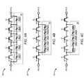
- FIG. 4A is a schematic diagram depicting a first embodiment of an RF switch branch that incorporates a plurality of series coupled harmonic cancellation circuits coupled across a corresponding one of a plurality of series coupled transistor switches making up the RF switch branch.
- FIG. 4B is a schematic diagram depicting a second embodiment of the RF switch branch that incorporates the plurality of series coupled harmonic cancellation circuits that are coupled across only a portion of the plurality of series coupled transistor switches excluding ones of the plurality of series coupled transistor switches adjacent to a first port and a second port of the RF switch branch.
- FIG. 4C is a schematic diagram depicting a third embodiment of the RF switch branch having degeneration resistors coupled between the plurality of series coupled harmonic cancellation circuits and the plurality of series coupled transistor switches.
- FIG. 5 is a schematic diagram depicting the RF switch branch depicted in FIG. 4C implemented using harmonic cancellation circuits based upon the harmonic cancellation circuit of FIG. 2B .
- FIG. 6 is a graph depicting a third harmonic generated by an off-state RF switch branch combined with an inverse phase third harmonic generated by a harmonic cancellation circuit.
- FIG. 7 is a graph depicting receiver power measured in dBm for a signal transmitted in band 17 (B17) versus band 4 (B4) input power as predicted by a simulation of the RF switch branch depicted in FIG. 4A .
- FIG. 8 is a graph showing the bounds of a one hundred run Monte Carlo simulation for process variation for harmonic cancellation according to the present disclosure.
- Off-state switches are slightly nonlinear and produce harmonics. Circuits of the present disclosure add other harmonic generators such that a set of combined harmonics cancel out.
- the present disclosure provides circuits having structures designed to provide third harmonic (H3) generation that cancels third harmonics generated by off-state switch branches.
- the presently disclosed circuits are directed to body-contacted switch branches.
- FIG. 1A is a schematic depicting a prior art RF switch branch 10 having a parallel bias scheme
- FIG. 1B is a schematic depicting a prior art RF switch branch 12 having a series bias scheme
- Both RF switch branch 10 and RF switch branch 12 are constructed using a series stack of NFETs M1-M5, with resistors R G , R B , R GC , and R BC setting a bias point for either an on-state or off-state operation.
- the present disclosure is specific to off-state cancellation of an H3 generated by RF switch branches such as RF switch branch 10 and RF switch branch 12 .
- the RF switch branch 10 can be put into an off-state by applying a gate voltage V G that is equal to a body voltage V B , and lower than the voltages at a first port RFA and a second port RFB. Moreover, if a voltage V RFA at the first port RFA and a voltage V RFB at the second port RFB are set to 0 V, and the gate voltage V G and the body voltage V B are set to ⁇ 2.5V, the RF switch branch 12 will be turned off.
- the RF switch branch 12 can be turned off by setting the voltage V RFA at the first port RFA and a voltage V RFB at the second port RFB are set to +2.5V, and the gate voltage V G and the body voltage V B are set to 0 V.
- Each field effect transistor (FET) in a stack of FETs making up either RF switch branch 10 or RF switch branch 12 that is in the off-state has an approximately equal part of a total RF voltage across the FET, and each FET acts as a nonlinear harmonic generator.
- source S and drain D terminals are at 0 V
- gate G and base B terminals are biased to a negative voltage.
- the RF voltage occurs across the source S terminals and drain D terminals.
- a basic circuit which generates a cancelling harmonic also uses one or more FET(s) and resistor(s).
- the FET and resistor technology can be the same FET and resistor technology used to construct the RF switch branch 10 and the RF switch branch 12 .
- a capacitance for each FET is relatively small, and nearly constant with voltage. However, there is a slight voltage dependent capacitance that urges a FET to generate harmonics.
- An exemplary change in capacitance measured for FETs typically used to implement the harmonic cancellation of the present disclosure is less than 1%.
- the voltage V in this case is the source-drain voltage.
- the nonlinearity responsible for generating a third harmonic is coefficient C2 of equation 1 above.
- a change of total capacitance for a first transistor and a second transistor making up a harmonic cancellation circuit ranges from around about 0.1% to around about 1%.
- the nonlinear capacitance C2 value ranges from around about 1 fF/V 2 to around about 3 fF/V 2 .
- FIGS. 2A , 2 B, and 2 C are schematics depicting three harmonic cancellation circuit variants that generate inverse phase H3 signals that are usable to cancel or at least reduce H3 signals generated by an RF switch branch such as RF switch branch 10 ( FIG. 1A ) or RF switch branch 12 ( FIG. 1B ).
- RF switch branch 10 FIG. 1A
- RF switch branch 12 FIG. 1B
- Each circuit depicted in FIGS. 2A , 2 B, and 2 C have practically identical parameters and a symmetrical die layout.
- resistors with the same element numbers/labels have practically identical values.
- FIG. 2A depicts a related art harmonic cancellation circuit 14 that is constructed with a first transistor M6 and a relatively identical second transistor M7 along with a first resistor R1 coupled between a first gate G1 and a second gate G2.
- the first transistor M6 and the second transistor M7 are each a field effect transistor (FET) type.
- the related art harmonic cancellation circuit 14 has a first coupling node A′ and a second coupling node B′ for coupling to additional harmonic cancellation circuits and for coupling to an RF switch branch for which H3 is to be cancelled.
- the voltages between source terminals S1 and S2, drain terminals D1 and D2, and body terminals B1 and B2 are equal.
- the first transistor M6 and the second transistor M7 are placed on a die (not shown) with symmetry so that there is no impact from second harmonic generation.
- the related art harmonic cancellation circuit 14 will produce out-of-phase third harmonics as long as the gate to source voltage for the FET does not exceed a threshold voltage VT.
- FIG. 2B is a schematic diagram depicting an embodiment of an improved harmonic cancellation circuit 16 that is in accordance with the present disclosure.
- a source-body voltage is not zero.
- a gate to source voltage V GS for the improved harmonic cancellation circuit 16 is reduced by more than one half if the voltage between the gate G1 and the gate G2 is the same as the voltage between the first coupling node A′ and the second coupling node B′ of the related art harmonic cancellation circuit 14 .
- the body-source bias changes the threshold voltage of the first transistor M6 and the second transistor M7, making it higher. In this way, neither the first transistor M6 nor the second transistor M7 reach their threshold voltage VT until a higher voltage across the first coupling node A′′ and the second coupling node B′′ is reached.
- FIG. 2C depicts a further improved embodiment, wherein the gate-source and source-body voltages can be tuned to provide more freedom, in particular, the voltage needed across a first coupling node A′′′ and a second coupling node B′′′ to reach a state wherein the gate to source voltage V GS equals the threshold voltage VT is even higher.
- the harmonic cancellation circuits shown in FIGS. 2B-3B can be further tuned by an application of a control voltage, as shown in FIGS. 3A and 3B .
- the resistors R1-R3 of the improved harmonic cancellation circuit 18 could be adjusted in value by replacing one or more of resistors R1-R3 with analog or digitally adjustable resistors, which are typically made up of a combination of resistors and FETs as known in the art.
- a resistance value of a resistor such as resistor R3 is made adjustable as shown in FIG. 3A .
- Resistance values for R1 range between around about 80 ohms to around about 1000 ohms
- R2 resistance values range between around about 480 ohms to 2000 ohms.
- Resistance values for R3 range from around about 80 ohms to around about 2000 ohms.
- Another method of tuning the circuit is to disconnect the source and drain of each of the first transistor M6 and the second transistor M7 from a resistor bias string made up of the resistors R1-R3, and connect the source and drain of each of the first transistor M6 and the second transistor M7 to bias inputs N1 and N2 for receiving biasing voltages V1 and V2, respectively.
- a position of a notch at which a maximum H3 cancellation occurs can be adjusted for input power, frequency, and temperature, etc.
- the input biases to V1 and V2 should be made through bias resistors, which can be implemented with the series bias scheme shown in FIG. 1B .
- FIGS. 4A , 4 B, and 4 C are schematics that depict several structures for RF switch branches having harmonic cancellation circuits.
- harmonic cancellation circuits such as the disclosed improved harmonic cancellation circuits 16 ( FIG. 2B ), 18 ( FIG. 2C ), 20 ( FIG. 3A ), and 22 ( FIG. 3B ) are represented by varactor symbols HC1-HC5.
- the gate bias resistors R G and body bias resistors R B are omitted for clarity.
- the same voltage that causes an RF switch branch 24 to generate an H3 signal is coupled to a harmonic cancellation block 26 made up of a plurality of series coupled harmonic cancellation circuits HC1-HC5.
- Each of the plurality of series coupled harmonic cancellation circuits HC1-HC5 are coupled across a corresponding one of plurality of series coupled transistor switches M1-M5 making up the RF switch branch 24 .
- An advantage of the configuration for the RF switch branch 24 is immunity to voltage stacking non-uniformity. Other combinations can also be used, such as two harmonic cancellation blocks per each transistor switch making up the RF switch branch 24 , etc.
- an RF switch branch 28 includes a harmonic cancellation block 30 that is connected at two nodes within the RF switch branch 28 .
- the plurality of series coupled harmonic cancellation circuits HC1-HC5 are coupled across only a portion of the plurality of series coupled transistor switches M1-M5 excluding ones of the plurality of series coupled transistor switches M1-M5 adjacent to a first port RFA and a second port RFB, which in this case excludes transistor switch M1 and transistor switch M5, respectively.
- FIG. 4C maintains the overall structure of RF switch branch 28 ( FIG. 4B ) in an RF switch branch 32 while also including degeneration resistors R DG1 and R DG2 in a harmonic cancellation block 34 to increase linearity of the RF switch branch 32 . Resistance values for degeneration resistors R DG1 and R DG2 range from around about 100 ohms to around about 10,000 ohms.
- FIG. 5 is a schematic diagram depicting the RF switch branch 32 depicted in FIG. 4C implemented using harmonic cancellation circuits based upon the improved harmonic cancellation circuit 16 ( FIG. 2B ).
- Each harmonic cancellation circuit HC1-HC3 is made up of the harmonic cancellation circuit 16 .
- any of the other harmonic cancellation circuits such as improved harmonic cancellation circuit 18 ( FIG. 2C ), harmonic cancellation circuit 20 ( FIG. 3A ), and harmonic cancellation circuit 22 ( FIG. 3B ) can be used to make up any of the harmonic cancellation circuits HC1-HC5 for the RF switch branch 24 ( FIG. 4A ), the RF switch branch 28 ( FIG. 4B ), and the RF switch branch 32 ( FIG. 4C ).
- FIG. 6 is a graph showing third harmonic production versus input power that results from the RF switch branch 24 ( FIG. 4A ) coupled with the harmonic cancellation circuit 22 ( FIG. 3B ).
- a magnitude of an H3 signal shown in dotted and dashed line
- an inverse phase H3 signal shown in dashed line
- the RF switch branch 24 produces an undesirable H3 signal that is closely matched by an inverse H3 signal generated by the harmonic cancellation circuit 22 over a desired input power (PIN) range.
- Resistances and transistor parameters for the harmonic cancellation circuit 22 are adjusted such that the harmonics of the harmonic cancellation circuit 22 are close to the harmonics generated by the plurality of series coupled transistor switches M1-M5 making up the RF switch branch 24 over a predetermined critical range of input voltages and/or input powers. Since the harmonic cancellation circuit 22 produces an H3 signal that is out of phase with the H3 signal generated by the plurality of series coupled transistor switches M1-M5 making up the RF switch branch 24 , a resultant H3 signal output to an RF system (not shown) associated with RF switch branch 24 is reduced.
- FIG. 7 is a graph depicting receiver power measured in dBm for a signal transmitted in band 17 (B17) versus band 4 (B4) input power as predicted by a simulation of the RF switch branch 24 depicted in FIG. 4A .
- a dotted and dashed straight line represents an H3 signal level for a relatively large RF switch branch and a dashed only straight line represents an H3 signal generated by a relatively smaller RF switch branch during operation of a band 17 (B17) transmit signal at a frequency of 710 MHz. These levels of H3 signal would degrade receiver sensitivity in an associated radio receiver in B4 (not shown).
- a relatively large reduction in H3 signal over an RF switch branch with a harmonic cancellation (HC) block is depicted by a star on a solid curved line at a critical input power of 24 dBm.
- B17 is a relatively large TX output signal at 710 MHz.
- the undesirable H3 is at three times 710 MHz, which at 2100 MHz is in the B4 RX band.
- the TX output signal generates an undesirable H3 signal in B4.
- This undesirable H3 signal is then interpreted by the receiver, which is located on the same phone, as a received signal.
- the TX output signal is sent on the same antenna that is receiving the B4 signal.
- the undesirable H3 signal of B17 is jamming the B4 RX.
- FIG. 8 is a graph showing the bounds of a one hundred run Monte Carlo simulation for process variation for harmonic cancellation circuits taught in accordance with the present disclosure. Although there is a lot of variation, notches and reduced H3 signal levels are sufficient to reduce the H3 typical RF applications. Additionally, FIG. 8 shows that in simulation, process variations do not seriously degrade the performance of the harmonic cancellation circuits and blocks taught by the present disclosure.
Landscapes
- Electronic Switches (AREA)
- Physics & Mathematics (AREA)
- Nonlinear Science (AREA)
Abstract
Description
C(V)=C0+V*C1+V*V*C2 (1)
Claims (24)
Priority Applications (1)
| Application Number | Priority Date | Filing Date | Title |
|---|---|---|---|
| US14/212,831 US9240770B2 (en) | 2013-03-15 | 2014-03-14 | Harmonic cancellation circuit for an RF switch branch |
Applications Claiming Priority (2)
| Application Number | Priority Date | Filing Date | Title |
|---|---|---|---|
| US201361789422P | 2013-03-15 | 2013-03-15 | |
| US14/212,831 US9240770B2 (en) | 2013-03-15 | 2014-03-14 | Harmonic cancellation circuit for an RF switch branch |
Publications (2)
| Publication Number | Publication Date |
|---|---|
| US20140266415A1 US20140266415A1 (en) | 2014-09-18 |
| US9240770B2 true US9240770B2 (en) | 2016-01-19 |
Family
ID=51524892
Family Applications (1)
| Application Number | Title | Priority Date | Filing Date |
|---|---|---|---|
| US14/212,831 Active 2034-07-18 US9240770B2 (en) | 2013-03-15 | 2014-03-14 | Harmonic cancellation circuit for an RF switch branch |
Country Status (1)
| Country | Link |
|---|---|
| US (1) | US9240770B2 (en) |
Cited By (4)
| Publication number | Priority date | Publication date | Assignee | Title |
|---|---|---|---|---|
| US20160085256A1 (en) * | 2014-02-18 | 2016-03-24 | Acco | Body Biasing for RF Switch Optimization |
| US20170288659A1 (en) * | 2016-03-31 | 2017-10-05 | Qorvo Us, Inc. | Apparatus with main transistor-based switch and on-state linearization network |
| DE102018211896A1 (en) * | 2018-07-17 | 2020-01-23 | Infineon Technologies Ag | RF switch |
| US11641204B2 (en) | 2020-12-31 | 2023-05-02 | Skyworks Solutions, Inc. | Switch linearization with asymmetrical anti-series varactor pair |
Families Citing this family (20)
| Publication number | Priority date | Publication date | Assignee | Title |
|---|---|---|---|---|
| USRE48965E1 (en) | 2005-07-11 | 2022-03-08 | Psemi Corporation | Method and apparatus improving gate oxide reliability by controlling accumulated charge |
| US20080076371A1 (en) * | 2005-07-11 | 2008-03-27 | Alexander Dribinsky | Circuit and method for controlling charge injection in radio frequency switches |
| US9236957B2 (en) * | 2013-05-07 | 2016-01-12 | Rf Micro Devices, Inc. | Technique to reduce the third harmonic of an on-state RF switch |
| US10491209B2 (en) * | 2013-07-17 | 2019-11-26 | Qualcomm Incorporated | Switch linearizer |
| CN103986450B (en) * | 2014-05-12 | 2017-04-12 | 华为技术有限公司 | Switch, tuner of antenna and radio frequency device |
| US10032731B2 (en) * | 2014-09-08 | 2018-07-24 | Skyworks Solutions, Inc. | Voltage compensated switch stack |
| US9503074B2 (en) | 2015-03-06 | 2016-11-22 | Qualcomm Incorporated | RF circuit with switch transistor with body connection |
| US10374595B1 (en) * | 2018-01-22 | 2019-08-06 | Infineon Technologies Ag | Self-adjustable RF switch cell |
| CN109088626B (en) * | 2018-07-21 | 2022-05-24 | 安徽矽磊电子科技有限公司 | Ultralow-power-consumption biased radio frequency switch |
| US11177802B2 (en) * | 2018-12-07 | 2021-11-16 | Skyworks Solutions, Inc. | Amplitude-phase canceling circuit for switch linearity |
| US10715133B1 (en) | 2019-05-30 | 2020-07-14 | Qorvo Us, Inc. | Radio frequency switch |
| US11296688B2 (en) | 2019-12-18 | 2022-04-05 | Skyworks Solutions, Inc. | Switching time reduction of an RF switch |
| CN112272017B (en) * | 2020-09-30 | 2022-04-05 | 锐石创芯(深圳)科技股份有限公司 | Radio frequency switch circuit |
| US11418190B2 (en) * | 2020-12-07 | 2022-08-16 | Nxp Usa, Inc. | Switch circuits and transistor stacks with capacitor networks for balancing off-state RF voltages and methods of their operation |
| US12028060B2 (en) * | 2021-06-17 | 2024-07-02 | Murata Manufacturing Co., Ltd. | Switch capacitance cancellation circuit |
| US11923884B2 (en) | 2021-09-24 | 2024-03-05 | Qualcomm Incorporated | Configurable harmonic rejection mixer (HRM) |
| US12160229B2 (en) | 2021-12-28 | 2024-12-03 | Skyworks Solutions, Inc. | Switching time reduction of an RF switch |
| US12199594B2 (en) | 2022-01-06 | 2025-01-14 | Skyworks Solutions, Inc. | Switching time reduction of an RF switch |
| CN116232296A (en) * | 2022-09-08 | 2023-06-06 | 上海迦美信芯通讯技术有限公司 | A RF Switching Circuit for Optimizing the Third Harmonic |
| CN119995574B (en) * | 2025-01-02 | 2025-10-31 | 锐石创芯(深圳)半导体有限公司 | RF switches, RF front-end modules and electronic devices |
Citations (13)
| Publication number | Priority date | Publication date | Assignee | Title |
|---|---|---|---|---|
| US20080079514A1 (en) * | 2006-10-02 | 2008-04-03 | Skyworks Solutions, Inc. | Harmonic phase tuning filter for RF switches |
| US20080290928A1 (en) * | 2007-05-24 | 2008-11-27 | Kabushiki Kaisha Toshiba | Switching circuit |
| US7492209B2 (en) * | 2006-04-17 | 2009-02-17 | Skyworks Solutions, Inc. | High-frequency switching device with reduced harmonics |
| US20090206910A1 (en) * | 2006-05-23 | 2009-08-20 | Nec Corporation | High-frequency switch circuit |
| US20100069020A1 (en) * | 2006-11-09 | 2010-03-18 | Renesas Technology Corp. | Semiconductor integrated circuit, rf module using the same, and radio communication terminal device using the same |
| US20100225377A1 (en) * | 2009-03-06 | 2010-09-09 | Nec Electronics Corporation | Switch circuit |
| US20110133816A1 (en) * | 2009-12-03 | 2011-06-09 | Nxp B.V. | Switch-body pmos switch with switch-body dummies |
| US20110260774A1 (en) * | 2010-04-27 | 2011-10-27 | Rf Micro Devices, Inc. | High power fet switch |
| US8461903B1 (en) * | 2009-09-11 | 2013-06-11 | Rf Micro Devices, Inc. | SOI switch enhancement |
| US20140062575A1 (en) * | 2012-08-29 | 2014-03-06 | Newport Fab, Llc Dba Jazz Semiconductor | RF Switch Branch Having Improved Linearity |
| US8786002B2 (en) * | 2010-06-29 | 2014-07-22 | Renesas Electronics Corporation | Semiconductor device |
| US20140335801A1 (en) * | 2013-05-07 | 2014-11-13 | Rf Micro Devices, Inc. | Technique to reduce the third harmonic of an on-state rf switch |
| US8922268B2 (en) * | 2012-07-07 | 2014-12-30 | Skyworks Solutions, Inc. | Adjustable gate and/or body resistance for improved intermodulation distortion performance of radio-frequency switch |
-
2014
- 2014-03-14 US US14/212,831 patent/US9240770B2/en active Active
Patent Citations (13)
| Publication number | Priority date | Publication date | Assignee | Title |
|---|---|---|---|---|
| US7492209B2 (en) * | 2006-04-17 | 2009-02-17 | Skyworks Solutions, Inc. | High-frequency switching device with reduced harmonics |
| US20090206910A1 (en) * | 2006-05-23 | 2009-08-20 | Nec Corporation | High-frequency switch circuit |
| US20080079514A1 (en) * | 2006-10-02 | 2008-04-03 | Skyworks Solutions, Inc. | Harmonic phase tuning filter for RF switches |
| US20100069020A1 (en) * | 2006-11-09 | 2010-03-18 | Renesas Technology Corp. | Semiconductor integrated circuit, rf module using the same, and radio communication terminal device using the same |
| US20080290928A1 (en) * | 2007-05-24 | 2008-11-27 | Kabushiki Kaisha Toshiba | Switching circuit |
| US20100225377A1 (en) * | 2009-03-06 | 2010-09-09 | Nec Electronics Corporation | Switch circuit |
| US8461903B1 (en) * | 2009-09-11 | 2013-06-11 | Rf Micro Devices, Inc. | SOI switch enhancement |
| US20110133816A1 (en) * | 2009-12-03 | 2011-06-09 | Nxp B.V. | Switch-body pmos switch with switch-body dummies |
| US20110260774A1 (en) * | 2010-04-27 | 2011-10-27 | Rf Micro Devices, Inc. | High power fet switch |
| US8786002B2 (en) * | 2010-06-29 | 2014-07-22 | Renesas Electronics Corporation | Semiconductor device |
| US8922268B2 (en) * | 2012-07-07 | 2014-12-30 | Skyworks Solutions, Inc. | Adjustable gate and/or body resistance for improved intermodulation distortion performance of radio-frequency switch |
| US20140062575A1 (en) * | 2012-08-29 | 2014-03-06 | Newport Fab, Llc Dba Jazz Semiconductor | RF Switch Branch Having Improved Linearity |
| US20140335801A1 (en) * | 2013-05-07 | 2014-11-13 | Rf Micro Devices, Inc. | Technique to reduce the third harmonic of an on-state rf switch |
Cited By (10)
| Publication number | Priority date | Publication date | Assignee | Title |
|---|---|---|---|---|
| US20160085256A1 (en) * | 2014-02-18 | 2016-03-24 | Acco | Body Biasing for RF Switch Optimization |
| US20170288659A1 (en) * | 2016-03-31 | 2017-10-05 | Qorvo Us, Inc. | Apparatus with main transistor-based switch and on-state linearization network |
| US10116298B2 (en) * | 2016-03-31 | 2018-10-30 | Qorvo Us, Inc. | Apparatus with main transistor-based switch and on-state linearization network |
| DE102018211896A1 (en) * | 2018-07-17 | 2020-01-23 | Infineon Technologies Ag | RF switch |
| DE102018211896B4 (en) | 2018-07-17 | 2020-06-25 | Infineon Technologies Ag | RF switch |
| US10734987B2 (en) | 2018-07-17 | 2020-08-04 | Infineon Technologies Ag | RF switch |
| DE102018211896B9 (en) * | 2018-07-17 | 2020-12-31 | Infineon Technologies Ag | RF switch |
| US11641204B2 (en) | 2020-12-31 | 2023-05-02 | Skyworks Solutions, Inc. | Switch linearization with asymmetrical anti-series varactor pair |
| US20250119139A1 (en) * | 2020-12-31 | 2025-04-10 | Skyworks Solutions, Inc. | Switch linearization with asymmetrical anti-series varactor pair |
| US12562737B2 (en) * | 2020-12-31 | 2026-02-24 | Skyworks Solutions, Inc. | Switch linearization with asymmetrical anti-series varactor pair |
Also Published As
| Publication number | Publication date |
|---|---|
| US20140266415A1 (en) | 2014-09-18 |
Similar Documents
| Publication | Publication Date | Title |
|---|---|---|
| US9240770B2 (en) | Harmonic cancellation circuit for an RF switch branch | |
| US9923594B2 (en) | Voltage swing uniformity in radio-frequency switches | |
| KR101712269B1 (en) | System and method for a radio frequency switch | |
| US8288895B2 (en) | High-power tunable capacitor | |
| US9899988B2 (en) | Switch, antenna tuner, and radio frequency apparatus | |
| US10630264B2 (en) | Attenuator | |
| US8994454B2 (en) | Amplifier circuit | |
| US10491209B2 (en) | Switch linearizer | |
| US9281802B2 (en) | System and method for a switchable capacitance | |
| Kwon et al. | A hybrid transformer-based CMOS duplexer with a single-ended notch-filtered LNA for highly integrated tunable RF front-ends | |
| EP3211792B1 (en) | Apparatus and methods for high linearity voltage variable attenuators | |
| US20160006409A1 (en) | Radio frequency switching system with improved linearity | |
| JP2015122628A (en) | Switching circuit and semiconductor module | |
| US11936357B2 (en) | Integrated isolator circuit in a time division duplex transceiver | |
| US9590561B2 (en) | Power amplifier | |
| US10469121B2 (en) | Non-linear shunt circuit for third order harmonic reduction in RF switches | |
| US10103712B2 (en) | Voltage variable attenuator, an integrated circuit and a method of attenuation | |
| US9166542B2 (en) | High frequency module and portable terminal using same |
Legal Events
| Date | Code | Title | Description |
|---|---|---|---|
| AS | Assignment |
Owner name: RF MICRO DEVICES, INC., NORTH CAROLINA Free format text: ASSIGNMENT OF ASSIGNORS INTEREST;ASSIGNORS:KERR, DANIEL CHARLES;BOLTON, ERIC K.;PHELPS, ROBERT ANDREW;SIGNING DATES FROM 20150930 TO 20151009;REEL/FRAME:036770/0958 |
|
| STCF | Information on status: patent grant |
Free format text: PATENTED CASE |
|
| AS | Assignment |
Owner name: QORVO US, INC., NORTH CAROLINA Free format text: MERGER;ASSIGNOR:RF MICRO DEVICES, INC.;REEL/FRAME:039196/0941 Effective date: 20160330 |
|
| FEPP | Fee payment procedure |
Free format text: MAINTENANCE FEE REMINDER MAILED (ORIGINAL EVENT CODE: REM.); ENTITY STATUS OF PATENT OWNER: LARGE ENTITY |
|
| FEPP | Fee payment procedure |
Free format text: SURCHARGE FOR LATE PAYMENT, LARGE ENTITY (ORIGINAL EVENT CODE: M1554); ENTITY STATUS OF PATENT OWNER: LARGE ENTITY |
|
| MAFP | Maintenance fee payment |
Free format text: PAYMENT OF MAINTENANCE FEE, 4TH YEAR, LARGE ENTITY (ORIGINAL EVENT CODE: M1551); ENTITY STATUS OF PATENT OWNER: LARGE ENTITY Year of fee payment: 4 |
|
| MAFP | Maintenance fee payment |
Free format text: PAYMENT OF MAINTENANCE FEE, 8TH YEAR, LARGE ENTITY (ORIGINAL EVENT CODE: M1552); ENTITY STATUS OF PATENT OWNER: LARGE ENTITY Year of fee payment: 8 |