US9240666B2 - Optical amplification device and method of controlling optical module - Google Patents
Optical amplification device and method of controlling optical module Download PDFInfo
- Publication number
- US9240666B2 US9240666B2 US14/257,298 US201414257298A US9240666B2 US 9240666 B2 US9240666 B2 US 9240666B2 US 201414257298 A US201414257298 A US 201414257298A US 9240666 B2 US9240666 B2 US 9240666B2
- Authority
- US
- United States
- Prior art keywords
- emission
- optical module
- input
- light
- optical
- Prior art date
- Legal status (The legal status is an assumption and is not a legal conclusion. Google has not performed a legal analysis and makes no representation as to the accuracy of the status listed.)
- Expired - Fee Related
Links
Images


Classifications
-
- H—ELECTRICITY
- H01—ELECTRIC ELEMENTS
- H01S—DEVICES USING THE PROCESS OF LIGHT AMPLIFICATION BY STIMULATED EMISSION OF RADIATION [LASER] TO AMPLIFY OR GENERATE LIGHT; DEVICES USING STIMULATED EMISSION OF ELECTROMAGNETIC RADIATION IN WAVE RANGES OTHER THAN OPTICAL
- H01S3/00—Lasers, i.e. devices using stimulated emission of electromagnetic radiation in the infrared, visible or ultraviolet wave range
- H01S3/05—Construction or shape of optical resonators; Accommodation of active medium therein; Shape of active medium
- H01S3/06—Construction or shape of active medium
- H01S3/063—Waveguide lasers, i.e. whereby the dimensions of the waveguide are of the order of the light wavelength
- H01S3/067—Fibre lasers
- H01S3/06754—Fibre amplifiers
-
- H—ELECTRICITY
- H01—ELECTRIC ELEMENTS
- H01S—DEVICES USING THE PROCESS OF LIGHT AMPLIFICATION BY STIMULATED EMISSION OF RADIATION [LASER] TO AMPLIFY OR GENERATE LIGHT; DEVICES USING STIMULATED EMISSION OF ELECTROMAGNETIC RADIATION IN WAVE RANGES OTHER THAN OPTICAL
- H01S5/00—Semiconductor lasers
- H01S5/06—Arrangements for controlling the laser output parameters, e.g. by operating on the active medium
- H01S5/068—Stabilisation of laser output parameters
- H01S5/06825—Protecting the laser, e.g. during switch-on/off, detection of malfunctioning or degradation
-
- H—ELECTRICITY
- H01—ELECTRIC ELEMENTS
- H01S—DEVICES USING THE PROCESS OF LIGHT AMPLIFICATION BY STIMULATED EMISSION OF RADIATION [LASER] TO AMPLIFY OR GENERATE LIGHT; DEVICES USING STIMULATED EMISSION OF ELECTROMAGNETIC RADIATION IN WAVE RANGES OTHER THAN OPTICAL
- H01S5/00—Semiconductor lasers
- H01S5/50—Amplifier structures not provided for in groups H01S5/02 - H01S5/30
- H01S5/5027—Concatenated amplifiers, i.e. amplifiers in series or cascaded
-
- H—ELECTRICITY
- H04—ELECTRIC COMMUNICATION TECHNIQUE
- H04B—TRANSMISSION
- H04B10/00—Transmission systems employing electromagnetic waves other than radio-waves, e.g. infrared, visible or ultraviolet light, or employing corpuscular radiation, e.g. quantum communication
- H04B10/29—Repeaters
- H04B10/291—Repeaters in which processing or amplification is carried out without conversion of the main signal from optical form
-
- H—ELECTRICITY
- H01—ELECTRIC ELEMENTS
- H01S—DEVICES USING THE PROCESS OF LIGHT AMPLIFICATION BY STIMULATED EMISSION OF RADIATION [LASER] TO AMPLIFY OR GENERATE LIGHT; DEVICES USING STIMULATED EMISSION OF ELECTROMAGNETIC RADIATION IN WAVE RANGES OTHER THAN OPTICAL
- H01S5/00—Semiconductor lasers
- H01S5/04—Processes or apparatus for excitation, e.g. pumping, e.g. by electron beams
- H01S5/041—Optical pumping
-
- H—ELECTRICITY
- H01—ELECTRIC ELEMENTS
- H01S—DEVICES USING THE PROCESS OF LIGHT AMPLIFICATION BY STIMULATED EMISSION OF RADIATION [LASER] TO AMPLIFY OR GENERATE LIGHT; DEVICES USING STIMULATED EMISSION OF ELECTROMAGNETIC RADIATION IN WAVE RANGES OTHER THAN OPTICAL
- H01S5/00—Semiconductor lasers
- H01S5/06—Arrangements for controlling the laser output parameters, e.g. by operating on the active medium
- H01S5/0617—Arrangements for controlling the laser output parameters, e.g. by operating on the active medium using memorised or pre-programmed laser characteristics
-
- H—ELECTRICITY
- H01—ELECTRIC ELEMENTS
- H01S—DEVICES USING THE PROCESS OF LIGHT AMPLIFICATION BY STIMULATED EMISSION OF RADIATION [LASER] TO AMPLIFY OR GENERATE LIGHT; DEVICES USING STIMULATED EMISSION OF ELECTROMAGNETIC RADIATION IN WAVE RANGES OTHER THAN OPTICAL
- H01S5/00—Semiconductor lasers
- H01S5/06—Arrangements for controlling the laser output parameters, e.g. by operating on the active medium
- H01S5/062—Arrangements for controlling the laser output parameters, e.g. by operating on the active medium by varying the potential of the electrodes
- H01S5/06209—Arrangements for controlling the laser output parameters, e.g. by operating on the active medium by varying the potential of the electrodes in single-section lasers
- H01S5/06216—Pulse modulation or generation
-
- H—ELECTRICITY
- H04—ELECTRIC COMMUNICATION TECHNIQUE
- H04B—TRANSMISSION
- H04B2210/00—Indexing scheme relating to optical transmission systems
- H04B2210/08—Shut-down or eye-safety
Definitions
- a certain aspect of embodiments described herein relates to an optical amplification device and a method of controlling an optical module.
- an optical module for optical amplification amplifies an optical signal in order to amplify a maximum output of the optical signal
- Document 1 Japanese Patent Application Publications No. 2005-244305 (hereinafter referred to as Document 1) and No. 2010-279956 (hereinafter referred to as Document 2) disclose a countermeasure against an erroneous light emission.
- Document 1 and Document 2 lack in safety measure during canceling an light emission.
- an optical amplification device including: an optical module that outputs an amplified light; and a controller that makes the optical module emit a light when an emission command is input into the controller, wherein the controller cancels an inputting of the emission command until a predetermined time passes, when a protection for forbidding a light emission of the optical module is canceled.
- a method of controlling an optical module comprising canceling inputting of an emission command until a predetermined time passes, when a protection for forbidding a light emission of an optical module that outputs an amplified light when a light emission command is input is canceled.
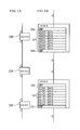
- FIG. 1A and FIG. 1B illustrate a schematic view of an optical transmission system to which an optical amplification device in accordance with an embodiment is applied;
- FIG. 2 illustrates a structure of an optical amplification device
- FIG. 3 illustrates a flowchart of an operation example of a control device
- FIG. 4 illustrates a time chart of an operation of a control device
- FIG. 5A and FIG. 5B illustrate a register-write test
- FIG. 5C and FIG. 5D illustrate a case where a plurality of estimations are sequentially performed.
- FIG. 6 illustrates a flowchart of another example of an operation of a control device
- FIG. 7 illustrates a flowchart of another example of an operation of a control device.
- FIG. 8A and FIG. 8B illustrate a time chart of an operation of a flowchart of FIG. 7 .
- FIG. 1A and FIG. 1B illustrate a schematic view of an optical transmission system to which an optical amplification device in accordance with an embodiment is applied.
- the optical transmission device has a structure in which an optical transmission device 200 provided in each station is coupled with each other via an optical fiber.
- the optical transmission device 200 has an optical amplification device 101 , a process device 102 , an optical amplification device 103 , and so on.
- the optical amplification device 101 amplifies an optical signal received from the optical transmission device 200 of another station to a power which the process device 102 can process.
- the process device 102 processes the optical signal amplified by the optical amplification device 101 .
- the optical amplification device 103 amplifies the optical signal processed by the process device 102 to a power allowing a transmission of the optical signal to a next station.
- FIG. 2 illustrates a structure of the optical amplification device 103 .
- the optical amplification device 103 has an optical module 10 , a control device 20 , a CPU 30 and so on.
- the optical module 10 is a module for outputting an amplified light, and has an optical amplifier 11 , a light source 12 and so on.
- the optical amplifier 11 amplifies a signal from the process device 102 with use of a light from the light source 12 .
- the optical amplifier 11 is a semiconductor optical amplifier.
- the light source 12 is, for example, a laser diode.
- the control device 20 is a control unit for controlling the optical module 10 .
- the control device 20 is, for example, structured with a FPGA (Field Programmable Gate Array) or the like.
- the CPU 30 is a Central Processing Unit. The CPU 30 performs a control of each device, collects an alarm or the like, and writes a command in a register of the control device 20 in accordance with an instruction from an outer component.
- the command written in the control device 20 by the CPU 30 includes a protection cancel command, an emission command and so on.
- the projection cancel command is a command for cancelling a protection prohibiting an emission of the optical module 10 .
- the emission command is a command for making the light source 12 emit a light.
- the protection cancel command and the emission command are written in a register of the control device 20 .
- the control device 20 prohibits the emission of the optical module 10 until a predetermined condition of the emission is satisfied, when the control device 20 receives a protection cancel command from the CPU 30 .
- the control device 20 activates an output enable for a predetermined time after a predetermined time passes after receiving the protection cancel command from the CPU 30 .
- the activation of the output enable is performed by an On/Off timer unit of the control device 20 .
- the control device 20 inputs an emission command that is input for a time when the output enable is activated into the light source 12 , and cancels the emission command that is input for a time when the output enable command is not activated.
- the light source 12 inputs a light into the optical amplifier 11 when the emission command is input from the control device 20 .
- a predetermined condition relating to an emission is that the emission command is input for a time when the output enable is activated.
- the optical module 10 emits a light when the predetermined condition is satisfied.
- FIG. 3 illustrates a flowchart of an operation example of the control device 20 .
- the control device 20 holds it until a protection cancel command is input by the CPU 30 (Step S 1 ).
- the control device 20 determines whether an output enable is activated or not
- Step S 2 When it is determined as “No” in the Step S 2 , the control device 20 cancels an emission command input by the CPU 30 (Step S 3 ). After the Step S 3 , the Step S 2 is executed again.
- Step S 4 the control device 20 determines whether an emission command is input or not.
- Step S 4 the Step S 2 is executed again.
- the control device 20 determines whether the output enable is activated or not (Step S 5 ).
- Step S 6 the control device 20 cancels the emission command confirmed in the Step S 4 (Step S 6 ).
- Step S 1 the Step S 1 is executed again.
- the control device 20 inputs an emission signal into the light source 12 (Step S 7 ).
- the light source 12 outputs a light to the optical amplifier 11 .
- the optical amplifier 11 amplifies the light and outputs the amplified light.
- FIG. 4 illustrates a time chart of an operation of the control device 20 .
- the control device 20 activates an output enable for a predetermined time after a predetermined time passes after inputting of a protection cancel command.
- the output enable is activated in a period A.
- An emission command for a period when the output enable is not activated is canceled.
- the control device 20 inputs an emission signal into the light source 12 when an emission command is input in the period A.
- the optical module 10 starts outputting of an optical signal.
- the optical outputting of the optical module 10 continues the optical outputting even if a period of the output enable is terminated.
- the optical module 10 cancels an emission command until a predetermined time passes after the protection is canceled.
- the emission is forbidden. Accordingly, a safety measure is taken when the emission is allowed. For example, an erroneous emission is prevented in a continuous access such as a register-write test.
- an emission command is canceled even if the emission command is input in a second estimation under a condition that a protection is missed in a first estimation, because an emission enable is limited to a predetermined period after a predetermined time passes. Therefore, an erroneous emission is prevented in a continuous test or the like.
- FIG. 5A and FIG. 5B illustrate the register-write test.
- an optical module when an emission command is input sequentially after a protection cancel command in the register-write test, an optical module emits a light under ordinary circumstances when an emission command is input.
- the emission command is canceled until a predetermined time passes after a protection is canceled. In this case, the optical module does not emit a light in a continuous access. Therefore, an erroneous emission is prevented.
- FIG. 5C and FIG. 5D illustrate a case where a plurality of estimations are sequentially performed.
- the optical module emits a light when an emission command is input, in a case where the emission command is input in a second estimation under a condition that a protection is missed in a first estimation.
- an emission command is canceled even if the emission command is input in a second estimation under a condition that a protection is missed in a first estimation. That is, a cancelling of the protection is required in every estimation. Therefore, an erroneous light emission is prevented.
- FIG. 6 illustrates a flowchart of another example of an operation of the control device 20 .
- the flowchart of FIG. 6 is executed when the optical module 10 starts to emit a light in the flowchart of FIG. 3 .
- an output enable is activated again for a predetermined time when a predetermined time (for example, one minute) passes after the last output enable is inactivated.
- the control device 20 determines whether the above-mentioned predetermined time passes or not after an emission signal is output (Step S 11 ). When it is determined as “No” in the Step S 11 , the Step S 11 is executed again.
- Step S 12 determines whether an output enable is activated or not.
- Step S 13 the control device 20 stops the light emission of the optical module 10 (Step S 13 ). After that, the execution of the flowchart is terminated.
- Step S 14 determines whether an emission command is input in a period when the output enable is activated.
- Step S 13 is executed.
- the control device 20 continues the light emission (Step S 15 ). After that, the execution of the flowchart is terminated. After the execution of the Step S 15 , the flowchart of FIG. 6 is executed again. In this way, an erroneous continuation of the light emission of the optical module 10 is prevented by confirming whether a predetermined condition of the light emission is satisfied at predetermined intervals when the optical output of the optical module 10 is started.
- FIG. 7 illustrates a flowchart of another example of an operation of the control device 20 .
- a flowchart of FIG. 7 is different from the flowchart of FIG. 3 in a point that Steps S 41 to S 43 are executed instead of the Step S 4 .
- the Steps S 41 to S 43 are described.
- the control device 20 determines whether an emission command 2 is input or not (Step S 42 ). When it is determined as “No” in the Step S 42 , the step S 1 is executed again. When it is determined as “Yes” in the Step S 42 , the control device 20 determines whether an emission command 3 is input or not (Step S 43 ). When it is determined as “No” in the Step S 43 , the Step S 1 is executed again. When it is determined as “Yes” in the Step S 43 , the control device 20 executes the Step S 5 . In this way, in the flowchart of FIG. 7 , the predetermined condition of the light emission is that a plurality of different emission commands are input in a predetermined order for a period when the output enable is activated.
- FIG. 8A and FIG. 8B illustrate a time chart of the operation of the flowchart of FIG. 7 .
- the control device 20 activates an output enable only for a predetermined period (a period A) after a predetermined time passes after a protection cancel command is input. An emission command for a period when the output enable is not activated is canceled.
- the control device 20 inputs an emission signal into the light source 12 .
- the optical module 10 starts to output an optical signal.
- the control device 20 cancels the emission signal.
- the predetermined condition is that a plurality of different emission commands are input in a predetermined order.
- the predetermined condition may be that a plurality of different emission commands are input regardless of the order.
- the emission of the optical module 10 may be stopped when a predetermined condition of the emission is confirmed at a predetermined interval and the predetermined condition is not satisfied, as well as the flowchart of FIG. 6 .
Landscapes
- Physics & Mathematics (AREA)
- Electromagnetism (AREA)
- Optics & Photonics (AREA)
- Condensed Matter Physics & Semiconductors (AREA)
- General Physics & Mathematics (AREA)
- Engineering & Computer Science (AREA)
- Computer Networks & Wireless Communication (AREA)
- Signal Processing (AREA)
- Plasma & Fusion (AREA)
- Optical Communication System (AREA)
- Semiconductor Lasers (AREA)
Abstract
Description
Claims (10)
Applications Claiming Priority (2)
| Application Number | Priority Date | Filing Date | Title |
|---|---|---|---|
| JP2013-104558 | 2013-05-16 | ||
| JP2013104558A JP2014225809A (en) | 2013-05-16 | 2013-05-16 | Optical amplifier and control method of optical module |
Publications (2)
| Publication Number | Publication Date |
|---|---|
| US20140340739A1 US20140340739A1 (en) | 2014-11-20 |
| US9240666B2 true US9240666B2 (en) | 2016-01-19 |
Family
ID=51895577
Family Applications (1)
| Application Number | Title | Priority Date | Filing Date |
|---|---|---|---|
| US14/257,298 Expired - Fee Related US9240666B2 (en) | 2013-05-16 | 2014-04-21 | Optical amplification device and method of controlling optical module |
Country Status (2)
| Country | Link |
|---|---|
| US (1) | US9240666B2 (en) |
| JP (1) | JP2014225809A (en) |
Citations (3)
| Publication number | Priority date | Publication date | Assignee | Title |
|---|---|---|---|---|
| US6583899B1 (en) * | 1998-12-31 | 2003-06-24 | Cisco Photonics Italy S.R.L. | Automatic protection system for an optical transmission system |
| US20050185957A1 (en) | 2004-02-24 | 2005-08-25 | Fujitsu Limited | Optical output control method for use in optical transmission node and optical output control apparatus for use in the same |
| JP2010279956A (en) | 2009-06-02 | 2010-12-16 | Miyachi Technos Corp | Laser processing equipment |
Family Cites Families (1)
| Publication number | Priority date | Publication date | Assignee | Title |
|---|---|---|---|---|
| DE69929934T2 (en) * | 1998-12-31 | 2006-08-10 | Cisco Systems International B.V. | Automatic protection system for an optical transmission system |
-
2013
- 2013-05-16 JP JP2013104558A patent/JP2014225809A/en active Pending
-
2014
- 2014-04-21 US US14/257,298 patent/US9240666B2/en not_active Expired - Fee Related
Patent Citations (5)
| Publication number | Priority date | Publication date | Assignee | Title |
|---|---|---|---|---|
| US6583899B1 (en) * | 1998-12-31 | 2003-06-24 | Cisco Photonics Italy S.R.L. | Automatic protection system for an optical transmission system |
| US20050185957A1 (en) | 2004-02-24 | 2005-08-25 | Fujitsu Limited | Optical output control method for use in optical transmission node and optical output control apparatus for use in the same |
| JP2005244305A (en) | 2004-02-24 | 2005-09-08 | Fujitsu Ltd | Optical output control method and optical output control apparatus in optical transmission node |
| US7519300B2 (en) * | 2004-02-24 | 2009-04-14 | Fujitsu Limited | Optical output control method for use in optical transmission node and optical output control apparatus for use in the same |
| JP2010279956A (en) | 2009-06-02 | 2010-12-16 | Miyachi Technos Corp | Laser processing equipment |
Also Published As
| Publication number | Publication date |
|---|---|
| JP2014225809A (en) | 2014-12-04 |
| US20140340739A1 (en) | 2014-11-20 |
Similar Documents
| Publication | Publication Date | Title |
|---|---|---|
| US8090993B2 (en) | I/O unit and industrial controller | |
| CN105637433B (en) | Control device and control method | |
| US9258062B2 (en) | Optical amplification device and optical amplification method | |
| ITSV20020056A1 (en) | DEVICE AND METHOD OF VERIFICATION OF LOGIC SOFTWARE MOTORS TO COMMAND RAILWAY SYSTEMS, IN PARTICULAR OF STATION SYSTEMS | |
| WO2005099342A3 (en) | A generic framework for runtime interception and execution control of interpreted languages | |
| AU2014385912B2 (en) | Air conditioner, air conditioner system, and rewrite control program | |
| US20190091864A1 (en) | Robot system | |
| US9240666B2 (en) | Optical amplification device and method of controlling optical module | |
| CN103901877B (en) | Breakdown judge based on fault attribute data and processing method | |
| EP4138314A4 (en) | OPTICAL MODULE AND PARAMETER TRANSMISSION METHOD, DETECTION METHOD AND CONTROL METHOD THEREOF AND FORWARD TRANSMISSION SYSTEM | |
| US9989936B2 (en) | Transport control system | |
| US11726066B2 (en) | Inspection device and inspection method | |
| KR102751245B1 (en) | Status notification device, control method of status notification device, information processing program, and recording medium | |
| US10083138B2 (en) | Controller, bus circuit, control method, and recording medium | |
| CA2674781C (en) | Optical communication device, optical communication system, optical output control method and program | |
| US9494999B2 (en) | Method for operating a bus control unit, and bus control unit | |
| KR101386821B1 (en) | Leakage signal cancellation apparatus of rfid system | |
| CN107677450B (en) | Method and system for detecting and responding to laser fault, storage medium and laser | |
| JP6263479B2 (en) | Signal transmission method and apparatus | |
| CN107577562B (en) | Data interaction method and device and computer readable storage medium | |
| KR102298846B1 (en) | Method of controlling radiographic imaging system | |
| US20080199179A1 (en) | Transmission system and system startup method | |
| EP4099105A1 (en) | Programmable device and control controller using the same | |
| US20140277657A1 (en) | Manufacturing system | |
| KR102329631B1 (en) | Diagnosis system and operation method thereof |
Legal Events
| Date | Code | Title | Description |
|---|---|---|---|
| AS | Assignment |
Owner name: FUJITSU LIMITED, JAPAN Free format text: ASSIGNMENT OF ASSIGNORS INTEREST;ASSIGNORS:KAWASHITA, MITSUYA;ZHANG, JINLIN;MAEDA, EIJI;AND OTHERS;SIGNING DATES FROM 20140314 TO 20140407;REEL/FRAME:032719/0420 |
|
| AS | Assignment |
Owner name: FUJITSU LIMITED, JAPAN Free format text: CORRECTIVE ASSIGNMENT TO CORRECT THE OMITTED SECOND ASSIGNEE TO FUJITSU TELECOM NETWORKS LIMITED PREVIOUSLY RECORDED ON REEL 032719 FRAME 0420. ASSIGNOR(S) HEREBY CONFIRMS THE ORIGINAL EXECUTED ASSIGNMENT;ASSIGNORS:KAWASHITA, MITSUYA;ZHANG, JINLIN;MAEDA, EIJI;AND OTHERS;SIGNING DATES FROM 20140314 TO 20140407;REEL/FRAME:033606/0031 Owner name: FUJITSU TELECOM NETWORKS LIMITED, JAPAN Free format text: CORRECTIVE ASSIGNMENT TO CORRECT THE OMITTED SECOND ASSIGNEE TO FUJITSU TELECOM NETWORKS LIMITED PREVIOUSLY RECORDED ON REEL 032719 FRAME 0420. ASSIGNOR(S) HEREBY CONFIRMS THE ORIGINAL EXECUTED ASSIGNMENT;ASSIGNORS:KAWASHITA, MITSUYA;ZHANG, JINLIN;MAEDA, EIJI;AND OTHERS;SIGNING DATES FROM 20140314 TO 20140407;REEL/FRAME:033606/0031 |
|
| AS | Assignment |
Owner name: FUJITSU LIMITED, JAPAN Free format text: ASSIGNMENT OF ASSIGNORS INTEREST;ASSIGNOR:FUJITSU TELECOM NETWORKS LIMITED;REEL/FRAME:037034/0241 Effective date: 20150930 |
|
| STCF | Information on status: patent grant |
Free format text: PATENTED CASE |
|
| FEPP | Fee payment procedure |
Free format text: MAINTENANCE FEE REMINDER MAILED (ORIGINAL EVENT CODE: REM.); ENTITY STATUS OF PATENT OWNER: LARGE ENTITY |
|
| LAPS | Lapse for failure to pay maintenance fees |
Free format text: PATENT EXPIRED FOR FAILURE TO PAY MAINTENANCE FEES (ORIGINAL EVENT CODE: EXP.); ENTITY STATUS OF PATENT OWNER: LARGE ENTITY |
|
| STCH | Information on status: patent discontinuation |
Free format text: PATENT EXPIRED DUE TO NONPAYMENT OF MAINTENANCE FEES UNDER 37 CFR 1.362 |
|
| FP | Lapsed due to failure to pay maintenance fee |
Effective date: 20200119 |