US9240427B2 - CFA resist silylation for limiting color interactions and improving crosstalk - Google Patents
CFA resist silylation for limiting color interactions and improving crosstalk Download PDFInfo
- Publication number
- US9240427B2 US9240427B2 US13/223,594 US201113223594A US9240427B2 US 9240427 B2 US9240427 B2 US 9240427B2 US 201113223594 A US201113223594 A US 201113223594A US 9240427 B2 US9240427 B2 US 9240427B2
- Authority
- US
- United States
- Prior art keywords
- color filter
- silylating agent
- color
- pattern
- groups
- Prior art date
- Legal status (The legal status is an assumption and is not a legal conclusion. Google has not performed a legal analysis and makes no representation as to the accuracy of the status listed.)
- Expired - Fee Related, expires
Links
- 230000003993 interaction Effects 0.000 title description 5
- 238000006884 silylation reaction Methods 0.000 title description 3
- 239000003795 chemical substances by application Substances 0.000 claims abstract description 92
- 239000000758 substrate Substances 0.000 claims abstract description 8
- 239000000049 pigment Substances 0.000 claims abstract description 4
- 229920002120 photoresistant polymer Polymers 0.000 claims description 22
- 239000000463 material Substances 0.000 claims description 18
- -1 acetoxy, mercapto, amino Chemical group 0.000 claims description 10
- 230000008021 deposition Effects 0.000 claims description 10
- WDVUXWDZTPZIIE-UHFFFAOYSA-N trichloro(2-trichlorosilylethyl)silane Chemical compound Cl[Si](Cl)(Cl)CC[Si](Cl)(Cl)Cl WDVUXWDZTPZIIE-UHFFFAOYSA-N 0.000 claims description 7
- 239000001056 green pigment Substances 0.000 claims description 5
- 125000001183 hydrocarbyl group Chemical group 0.000 claims description 5
- 125000000217 alkyl group Chemical group 0.000 claims description 4
- 125000003118 aryl group Chemical group 0.000 claims description 4
- 150000001875 compounds Chemical class 0.000 claims description 4
- 239000001054 red pigment Substances 0.000 claims description 4
- 239000001055 blue pigment Substances 0.000 claims description 3
- 125000000962 organic group Chemical group 0.000 claims description 3
- WGGNJZRNHUJNEM-UHFFFAOYSA-N 2,2,4,4,6,6-hexamethyl-1,3,5,2,4,6-triazatrisilinane Chemical compound C[Si]1(C)N[Si](C)(C)N[Si](C)(C)N1 WGGNJZRNHUJNEM-UHFFFAOYSA-N 0.000 claims description 2
- 229910007266 Si2O Inorganic materials 0.000 claims description 2
- NIXOWILDQLNWCW-UHFFFAOYSA-M acrylate group Chemical group C(C=C)(=O)[O-] NIXOWILDQLNWCW-UHFFFAOYSA-M 0.000 claims description 2
- 125000003342 alkenyl group Chemical group 0.000 claims description 2
- 125000004093 cyano group Chemical group *C#N 0.000 claims description 2
- 125000000524 functional group Chemical group 0.000 claims description 2
- 125000005843 halogen group Chemical group 0.000 claims 1
- 238000000151 deposition Methods 0.000 abstract description 13
- 238000000034 method Methods 0.000 abstract description 4
- 239000000126 substance Substances 0.000 description 14
- 238000005229 chemical vapour deposition Methods 0.000 description 12
- 239000010410 layer Substances 0.000 description 10
- 230000003287 optical effect Effects 0.000 description 7
- XUIMIQQOPSSXEZ-UHFFFAOYSA-N Silicon Chemical group [Si] XUIMIQQOPSSXEZ-UHFFFAOYSA-N 0.000 description 6
- KPUWHANPEXNPJT-UHFFFAOYSA-N disiloxane Chemical class [SiH3]O[SiH3] KPUWHANPEXNPJT-UHFFFAOYSA-N 0.000 description 6
- 238000003491 array Methods 0.000 description 5
- 238000007385 chemical modification Methods 0.000 description 5
- 239000000203 mixture Substances 0.000 description 5
- 230000007547 defect Effects 0.000 description 4
- BLRPTPMANUNPDV-UHFFFAOYSA-N Silane Chemical group [SiH4] BLRPTPMANUNPDV-UHFFFAOYSA-N 0.000 description 3
- 239000006227 byproduct Substances 0.000 description 3
- 239000003086 colorant Substances 0.000 description 3
- 238000004132 cross linking Methods 0.000 description 3
- 239000003431 cross linking reagent Substances 0.000 description 3
- 238000003618 dip coating Methods 0.000 description 3
- 238000004519 manufacturing process Methods 0.000 description 3
- 230000004048 modification Effects 0.000 description 3
- 238000012986 modification Methods 0.000 description 3
- 229920000642 polymer Polymers 0.000 description 3
- 229920005989 resin Polymers 0.000 description 3
- 239000011347 resin Substances 0.000 description 3
- 229910000077 silane Inorganic materials 0.000 description 3
- 229910052710 silicon Inorganic materials 0.000 description 3
- 238000004528 spin coating Methods 0.000 description 3
- 238000007740 vapor deposition Methods 0.000 description 3
- 241001428800 Cell fusing agent virus Species 0.000 description 2
- 241000579895 Chlorostilbon Species 0.000 description 2
- UFHFLCQGNIYNRP-UHFFFAOYSA-N Hydrogen Chemical compound [H][H] UFHFLCQGNIYNRP-UHFFFAOYSA-N 0.000 description 2
- BOTDANWDWHJENH-UHFFFAOYSA-N Tetraethyl orthosilicate Chemical compound CCO[Si](OCC)(OCC)OCC BOTDANWDWHJENH-UHFFFAOYSA-N 0.000 description 2
- 230000015572 biosynthetic process Effects 0.000 description 2
- 238000006243 chemical reaction Methods 0.000 description 2
- IJOOHPMOJXWVHK-UHFFFAOYSA-N chlorotrimethylsilane Chemical compound C[Si](C)(C)Cl IJOOHPMOJXWVHK-UHFFFAOYSA-N 0.000 description 2
- 230000007423 decrease Effects 0.000 description 2
- 229910052876 emerald Inorganic materials 0.000 description 2
- 239000010976 emerald Substances 0.000 description 2
- FFUAGWLWBBFQJT-UHFFFAOYSA-N hexamethyldisilazane Chemical compound C[Si](C)(C)N[Si](C)(C)C FFUAGWLWBBFQJT-UHFFFAOYSA-N 0.000 description 2
- 239000001257 hydrogen Substances 0.000 description 2
- 229910052739 hydrogen Inorganic materials 0.000 description 2
- 238000003384 imaging method Methods 0.000 description 2
- 208000036971 interstitial lung disease 2 Diseases 0.000 description 2
- 230000009467 reduction Effects 0.000 description 2
- 150000004756 silanes Chemical class 0.000 description 2
- 239000004971 Cross linker Substances 0.000 description 1
- 230000004075 alteration Effects 0.000 description 1
- 125000003368 amide group Chemical group 0.000 description 1
- 125000003277 amino group Chemical group 0.000 description 1
- 230000008901 benefit Effects 0.000 description 1
- 125000003178 carboxy group Chemical group [H]OC(*)=O 0.000 description 1
- 238000000576 coating method Methods 0.000 description 1
- 238000009833 condensation Methods 0.000 description 1
- 230000005494 condensation Effects 0.000 description 1
- 238000012864 cross contamination Methods 0.000 description 1
- 230000001419 dependent effect Effects 0.000 description 1
- OSXYHAQZDCICNX-UHFFFAOYSA-N dichloro(diphenyl)silane Chemical compound C=1C=CC=CC=1[Si](Cl)(Cl)C1=CC=CC=C1 OSXYHAQZDCICNX-UHFFFAOYSA-N 0.000 description 1
- 238000009792 diffusion process Methods 0.000 description 1
- 150000004820 halides Chemical group 0.000 description 1
- 125000004435 hydrogen atom Chemical group [H]* 0.000 description 1
- 230000007062 hydrolysis Effects 0.000 description 1
- 238000006460 hydrolysis reaction Methods 0.000 description 1
- 125000002887 hydroxy group Chemical group [H]O* 0.000 description 1
- 239000007788 liquid Substances 0.000 description 1
- 238000005259 measurement Methods 0.000 description 1
- 125000004430 oxygen atom Chemical group O* 0.000 description 1
- 239000011241 protective layer Substances 0.000 description 1
- 239000004065 semiconductor Substances 0.000 description 1
- 238000000926 separation method Methods 0.000 description 1
- 239000010703 silicon Substances 0.000 description 1
- 238000001228 spectrum Methods 0.000 description 1
- 238000006467 substitution reaction Methods 0.000 description 1
- QHAHOIWVGZZELU-UHFFFAOYSA-N trichloro(trichlorosilyloxy)silane Chemical compound Cl[Si](Cl)(Cl)O[Si](Cl)(Cl)Cl QHAHOIWVGZZELU-UHFFFAOYSA-N 0.000 description 1
- DENFJSAFJTVPJR-UHFFFAOYSA-N triethoxy(ethyl)silane Chemical compound CCO[Si](CC)(OCC)OCC DENFJSAFJTVPJR-UHFFFAOYSA-N 0.000 description 1
- 239000005051 trimethylchlorosilane Substances 0.000 description 1
Images


Classifications
-
- H—ELECTRICITY
- H01—ELECTRIC ELEMENTS
- H01L—SEMICONDUCTOR DEVICES NOT COVERED BY CLASS H10
- H01L27/00—Devices consisting of a plurality of semiconductor or other solid-state components formed in or on a common substrate
- H01L27/14—Devices consisting of a plurality of semiconductor or other solid-state components formed in or on a common substrate including semiconductor components sensitive to infrared radiation, light, electromagnetic radiation of shorter wavelength or corpuscular radiation and specially adapted either for the conversion of the energy of such radiation into electrical energy or for the control of electrical energy by such radiation
- H01L27/144—Devices controlled by radiation
- H01L27/146—Imager structures
- H01L27/14601—Structural or functional details thereof
- H01L27/1462—Coatings
- H01L27/14621—Colour filter arrangements
-
- H—ELECTRICITY
- H01—ELECTRIC ELEMENTS
- H01L—SEMICONDUCTOR DEVICES NOT COVERED BY CLASS H10
- H01L27/00—Devices consisting of a plurality of semiconductor or other solid-state components formed in or on a common substrate
- H01L27/14—Devices consisting of a plurality of semiconductor or other solid-state components formed in or on a common substrate including semiconductor components sensitive to infrared radiation, light, electromagnetic radiation of shorter wavelength or corpuscular radiation and specially adapted either for the conversion of the energy of such radiation into electrical energy or for the control of electrical energy by such radiation
- H01L27/144—Devices controlled by radiation
- H01L27/146—Imager structures
- H01L27/14601—Structural or functional details thereof
- H01L27/14625—Optical elements or arrangements associated with the device
- H01L27/14627—Microlenses
-
- H—ELECTRICITY
- H04—ELECTRIC COMMUNICATION TECHNIQUE
- H04N—PICTORIAL COMMUNICATION, e.g. TELEVISION
- H04N25/00—Circuitry of solid-state image sensors [SSIS]; Control thereof
- H04N25/10—Circuitry of solid-state image sensors [SSIS]; Control thereof for transforming different wavelengths into image signals
- H04N25/11—Arrangement of colour filter arrays [CFA]; Filter mosaics
- H04N25/13—Arrangement of colour filter arrays [CFA]; Filter mosaics characterised by the spectral characteristics of the filter elements
- H04N25/134—Arrangement of colour filter arrays [CFA]; Filter mosaics characterised by the spectral characteristics of the filter elements based on three different wavelength filter elements
-
- H—ELECTRICITY
- H04—ELECTRIC COMMUNICATION TECHNIQUE
- H04N—PICTORIAL COMMUNICATION, e.g. TELEVISION
- H04N23/00—Cameras or camera modules comprising electronic image sensors; Control thereof
- H04N23/10—Cameras or camera modules comprising electronic image sensors; Control thereof for generating image signals from different wavelengths
-
- H04N9/045—
Definitions
- the invention described herein relates generally to imaging devices and, more specifically, to novel color filter arrays for use in electronic imagers to limit color interactions, improve crosstalk and limit optical loss.
- a single image sensor can be a pixel array wherein each pixel includes a photo sensor which generates photoelectrons from photons. Additional circuitry next to each photo sensor converts the photoelectrons to a voltage. Extra circuitry on the pixel array may be included to convert the voltage to digital data.
- a color filter array on a pixel array enables each pixel or photo sensor to capture the intensity of light across a color spectrum.
- a microlens array is generally placed over the color filter array to focus the received light onto the photo sensors.
- Color filter arrays and microlenses used in electronic imagers and sensors are often made of photoresist material. Different chemicals may be used to give the material desired property variations to be suitable for use as color filters.
- certain mechanical and chemical properties of the photoresist material such as hardness, chemical resistance, durability, resistance to humidity and other atmospheric stresses, determine the selection of a photoresist material.
- Chemical and physical changes may occur in the exposed areas of the photoresist layer. For example, chemical bonds may be formed or destroyed between some of adjacent photoresist color filters causing defects at the surface of the color filter array.
- crosstalk a phenomenon where photon or electron leakages cause an interaction between neighboring pixels, increases as the distances between pixels decreases.
- the nature of the crosstalk in image sensors has various origins: electron diffusion in the photo screen, insufficient optical separation of pixels or even electrical crosstalk in the readout sensor.
- the crosstalk in image sensors can desaturate colors and blur image details. Thus, when crosstalk occurs, resolution decreases in the image sensor, causing distortion in images produced by the sensor.
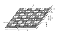
- FIG. 1 is a perspective view of a color filter array (CFA) in an electronic imager according to an embodiment of the invention.
- CFA color filter array
- FIG. 2 is a cross-sectional view of the color filter array in the electronic imager according to the invention taken along the line I-II in FIG. 1 .
- FIG. 3 is a top view of the color filter array in the electronic imager according to the invention.
- FIG. 4 is a SEM (scanning electron microscope) image of the color filter array (CFA) showing the silylating agent causes a cross linking of the photoresist material according to the invention.
- FIG. 5 is a graph of quantum efficiency versus wavelength showing reduced crosstalk between pixels according to an embodiment of the invention.
- FIG. 6 is a graph of quantum efficiency versus wavelength showing reduced crosstalk between pixels according to another embodiment of the invention.
- FIGS. 7A and 7B are sectional views of other alternative embodiments of the color filter array.
- FIGS. 8A , 8 B and 8 C are sectional views of a microlens array disposed on different embodiments of the color filter array in the electronic imager according to the invention.
- FIGS. 9A , 9 B and 9 C are sectional views of the silylating agent formed on a microlens array disposed on different embodiments of the color filter array in the electronic imager according to the invention.
- FIGS. 10A , 10 B, 10 C, 10 D and 10 E are perspective views illustrating a method of manufacturing the color filter array in the electronic imager according to the invention.
- FIG. 11 is a sectional view illustrating the method of manufacturing the color filter array in the electronic imager according to the invention taken along the line III-IV in FIG. 10D , wherein a silylating agent is formed on a first color pattern of the color filter array.
- FIG. 12 is a sectional view illustrating the method of manufacturing the color filter array in the electronic imager according to the invention taken along the line V-VI in FIG. 10E , wherein a silylating agent is formed on a first color pattern of the color filter array.
- the photoresist materials are inherently soft (on a hardness scale) and also of refractive index, e.g., 1.63. It is desirable to modify the CFAs, particularly in their outer layers, to make a harder and lower refraction index CFAs to limit optical losses.
- FIG. 1 to FIG. 3 An example of a color filter array (CFA) 1 in an electronic imager according to the present invention, as illustrated in FIG. 1 to FIG. 3 , is provided with a substrate 10 , a pixel sensor array 20 (shown in FIGS. 2 and 10A ), a plurality elements 300 of the color filter array 1 and a silylating agent 40 .
- the pixel sensor array 20 is formed on the substrate 10 .
- the plurality elements 300 of the color filter array 1 containing respective pigments form multiple color filter patterns 30 on the pixel sensor array 20 .
- the multiple color filter patterns 30 include a first color pattern 31 , a second color pattern 32 and a third color pattern 33 .
- the silylating agent 40 is formed between the first color filter pattern 31 and the second/third color patterns 32 , 33 of the multiple color patterns 30 .
- FIG. 1 to FIG. 3 illustrate the silylating agent 40 being formed between the first color filter pattern 31 and the second/third color patterns 32 , 33
- the silylating agent 40 can also be formed on each individual element 300 of the color filter array 1 .
- the multiple different color filter patterns 30 may be formed on the color filter array 1 including employing different color filters and arranging these color filters into different patterns.
- a Bayer pattern of RGBG is selected.
- color filter arrays having non-Bayer patterns are also applicable.
- Those non-Bayer patterns include alternative color filter array to the Bayer pattern, and/or non-conventional patterns, colors and sequences for the color deposition.
- non-Bayer patters examples include RGBE pattern (red, green, blue, emerald), CYGM pattern (cyan, yellow, green, magenta), CYYM filter (one cyan, two yellow, and one magenta), RGBW pattern (red, green, blue, white), CMYW pattern (cyan, magenta, yellow, and white), RGBW Bayer pattern (traditional RGBW similar to Bayer and RGBE patterns), and any other existing and prospective color filter patterns.
- the multiple color filter patterns 30 include the first color pattern 31 having elements 301 that contain a green pigment, the second color pattern 32 having elements 302 that contain a red pigment and the third color pattern 33 having elements 303 that contain a blue pigment.
- the plurality elements 300 of the color filter array 1 includes the elements 301 that contain the green pigment, the elements 302 that contain the red pigment and the elements 303 that contains the blue pigment.
- the pixel array 20 has pixel elements 200 .
- the example pixel elements 200 include pixel elements 201 and pixel elements 202 .
- the first color pattern 31 is formed on the pixel elements 201 .
- the second color pattern 31 and the third color pattern 32 are formed on the pixel elements 202 .
- the pixel elements 200 is illustrated as cubical structure, any other shapes and sizes may be applied.
- the silylating agent 40 is formed on the first color pattern 31 containing the green pigment and also formed on the pixel elements 202 between respective elements 301 of the first color pattern 31 .
- the silylating agent 40 includes a side portion 41 formed on vertical sides of the elements 301 of the first color pattern 31 , a top portion 42 formed on the top side of the elements 301 of the first color pattern 31 and a bottom portion 43 formed on the top side of the pixel elements 202 between the respective elements 301 of the first color pattern 31 .
- Each individual element 302 of the second color pattern 32 and each individual element 303 of the third color pattern 33 (not shown in FIG.
- the side portions 41 form a boundary layer 44 between each individual element 300 of the color filter array 1 , which prevents the elements 301 , 302 and 303 of the color filter array 1 from reacting with each other.
- some elements 301 , 302 and 303 of the color filter array 1 may react with each other producing crystalline byproducts that may cause defects at the surface of the color filter array 1 , and at the interfaces of the individual pixel elements 200 .
- the chemical silylation modification with the silylating agent 40 on the color filter array 1 prevents each elements 301 , 302 and 303 of the color filter array 1 from reacting with the surrounded elements, so as to limit the photoresist interaction.
- a silylating agent is a silane that substitutes an active hydrogen in an organic molecule including polymers and resins with an organosilicon group to form a siloxane.
- the active hydrogen is usually hydroxyl group, amino group, carboxyl group, or amide group and the silane is usually a compound that contains at least one silicon atom.
- One of the purposes of substitution is to protect reactive group during chemical reaction.
- silanes are used as cross linking agents to form siloxanes to improve chemical resistances.
- the cross-linking agent is a compound that has the capability to chemically connect other molecules in order to create a network of molecules linked together.
- Siloxanes are compounds composed of units of the form R 2 SiO, where R is a hydrogen atom or a hydrocarbon group, with branched or unbranched backbones consisting of alternating silicon and oxygen atoms —Si—O—Si—O—, with side chains R attached to the silicon atoms.
- the siloxanes have many properties including chemical resistance, tunable refractive index, tunable mechanical properties, excellent photo-stability and good thermal stability.
- Siloxanes polymers and resins can be viewed as organic-inorganic hybrids that combine many desirable properties of conventional organic and inorganic components. Many of the optical, electrical, and mechanical properties of siloxane materials can be efficiently tuned through a combination of organic groups and material structures.
- the refractive index of a siloxane polymer is composition dependent and generally ranges from 1.4 to 1.54. Introduction of composition modification can further expand, the refractive index range to between 1.15 and 1.63.
- the siloxanes are generally prepared by hydrolysis and condensation of a chloro- or alkoxy silanes.
- the silylating agent 40 in the present invention used to create the boundary layers 44 on the color filter array 1 is a silane cross-linking agent containing at least one silicon atom.
- 1,2-Bis(trichlorosilyl)ethane, Cl 3 SiCH 2 CH 2 SiCl 3 is used as the silylating agent 40 .
- Cl 3 SiCH 2 CH 2 SiCl 3 used herein functions as a cross linker having a linking ability to chemically bond the photoresist material together, i.e.
- Cl 3 SiCH 2 CH 2 SiCl 3 is a colorless, transparent liquid at room temperature and can be deposited on the color filter array 1 by means of vapor deposition or solution deposition.
- silylating agents in the present invention include the silanes contain silicon atoms, and the mixture thereof. These silylating agents have general formula as follows. SiR x (OR′) 4-x , SiR x (O 2 R′) 4-x , SiCl y R 4-y , Si 2 O(OR) 6 , Si 2 OCl y R 4-y , Si 3 O 2 Cl y R 8-y
- R and R′ stand for independently substituted or unsubstituted hydrocarbyl groups including alkyl groups, aryl groups, halogenated alkyl groups, halogenated aryl groups or alkenyl groups, or organic groups having a (meth)acryloxy, acetoxy, mercapto, amino or cyano group.
- Examples of the useful silylating agents are (tetraethoxy)silane (Si(OC 2 H 5 ) 4 ), hexachlorodisiloxane (Si 2 OCl 6 ), ethyltriethoxysilane (Si(OC 2 H 5 ) 3 (C 2 H 5 )), diphenyldichlorosilane (Si(C 6 H 5 ) 2 Cl 2 ).
- the letter “x” and “y” are each independently 0, 1, 2, 3, or 4.
- trisilanes containing three silicon atoms include trisilanes containing three silicon atoms.
- An example of trisilanes is a silazanes, hexamethylcyclotrisilazane C 6 H 21 N 3 Si 3 .
- silylating agents may be used.
- a mixture of trimethylchlorosilane and hexamethyldisilazane may be more reactive than either silylating agent alone.
- the chemical modification of the multiple color filter patterns 30 employing the silylating agent 40 to form siloxanes between at least one color filter pattern of the multiple color filter patterns 30 provides useful properties of the color filter array 1 in electronic imagers. Those properties include hardness, lower refractive index compared to the photoresist materials, chemical resistance, and good thermal stability.
- FIG. 4 is a scanning electron microscope (SEM) image showing the boundary layer 44 formed with Cl 3 SiCH 2 CH 2 SiCl 3 by chemical vapor deposition (CVD).
- silylating agent formation on the color filter array 1 is that the silylation of the color filter array 1 , in particular, forming the bottom portion 43 of the silylating agent 40 on the pixel elements 202 , has been shown to improve the optical crosstalk between the pixel elements 200 .
- An 1% reduction in cross-talk reduction is achieved, as shown in the quantum efficiency (QE) measurements shown in FIGS. 5 and 6 .
- much higher blue QE, higher red QE toward longer wavelength and slightly lower green QE may be obtained with silylating agent deposited by chemical vapor deposition (CVD).
- the slightly lower green QE is due to thicker green filters. Thinner green filters may increase the QE peak of the green filters.
- the overall cross-talk may be reduced from 12% to 10.56%.
- the QE peak and QE width toward longer wavelength of the red filters may be increased consistently and significantly with silylating agent deposited by CVD due to less cross contamination from the green photoresist material.
- the cross-talk for example, may be reduced by 1%.
- the green QE peak is lower with silylating agent deposited by CVD is because of thicker green filters. With adjustment of thickness, the green QE peak may be recovered.
- the silylating agent 50 includes a side portion 51 formed on vertical sides of the elements 301 of the first color pattern 31 and a bottom portion 53 formed on the top side of the pixel elements 202 between the respective elements 301 of the first color pattern 31 .
- the silylating agent is not formed on the top of the first color pattern 31 .
- This structure may be formed, for example by planarization the surface after depositing the red and blue filters to remove the silylating agent from the top of the green filter.
- Example thicknesses of the green, red and blue filters are from 500 nm to 1 um.
- the thicknesses of the green, red and blue filters can be anything in between 500 nm and 1 um and do not have to be same for each color, as shown in FIGS. 7A , 8 B and 9 B.
- the silylating agent 60 includes a side portion 61 formed on vertical sides of the elements 301 of the first color pattern 31 , a first top portion 62 formed on the top side of each individual elements 301 of the first color pattern 31 , a bottom portion 63 formed on the top side of the pixel elements 202 between the respective elements 301 of the first color pattern 31 and a second top portion 64 formed on the top side of each individual elements 302 of the second color pattern 32 and each individual element 303 of the third color pattern 33 (not shown in FIG. 7B ).
- the silylating agent 60 is additionally formed on the top of the elements 302 of the second color pattern 32 and on the top of the elements 303 of the third color pattern 33 .
- a microlens array 70 may be disposed on the color filter array 1 .
- the microlens array 70 includes a plurality of microlenses 700 disposed on the color filter array 1 .
- each individual microlens 700 is disposed on each individual color element 300 .
- the silylating agent 40 includes the side portion 41 , the top portion 42 and the bottom portion 43 .
- each individual microlens 700 is disposed on each individual color element 300
- the silylating agent 50 includes the side portion 51 and the bottom portion 53 .
- each individual microlens 700 is disposed on each individual color element 300 , and the silylating agent 60 includes the side portion 61 , the first top portion 62 , the bottom portion 63 and the second top portion 64 .
- the chemical modification using the silylating agent may also be applied to the microlens array 70 to form a microlens array that is harder and has a lower refractive index.
- the silylating agent 80 is formed on the microlens array 70 by means of vapor deposition, for example in an CVD chamber, or solution deposition.
- FIG. 9A shows the microlens array 70 with the silylating agent 80 disposed on the embodiment of the color filter array 1 , shown in FIG. 2 .
- FIG. 9B shows the microlens array 70 with the silylating agent 80 disposed on another embodiment of the color filter array 1 , shown in FIG. 7A .
- FIG. 9C shows the microlens array 70 with the silylating agent 80 disposed on yet another embodiment of the color filter array 1 , shown in FIG. 7B .
- the silylating agent may be further hydrolyzed or oxidized, either during the deposition, or prior to the application of the silylating agent, forming a siloxane.
- the silylating agent may be formed in a very thin layer on individual color filters, on one or more color filter patterns, on microlenses, and on pixel sensors having many different sizes and shapes.
- the example silylating agents react with the photoresist materials and generates a cross-linking of the photoresist materials so as to create a boundary protective layer to prevent the color filters from reacting with each other.
- the color filter interaction in the color filter array 1 is limited.
- the silylating agent deposited on the surface of the color filters or the color filter patterns or the pixels has a thickness in the range of 1 nanometer to 1000 nanometer. In example embodiments, the silylating agent deposited on the surface of the color filters or the color filter patterns or the pixels has a thickness in the range of 5 nanometer to 20 nanometer.
- the pixel array 20 may be formed in the substrate 10 such that each pixel element 200 is embedded in the substrate 10 .
- the first color pattern 31 containing green pigment is disposed on the pixel array 20 .
- the elements 301 of the first color pattern 31 are alternately disposed on respective pixel elements 201 , as shown in FIG. 10B .
- the silylating agent 40 is deposited on the first color filter pattern 31 after disposing the first color filter pattern 31 on the pixel sensor array 20 , as shown in FIG. 10C .
- the silylating agent 40 may be deposited on the first color pattern 31 by means of vapor deposition, for example CVD in a CVD chamber, or by solution deposition including spin-coating or dip-coating in a chemical bath.
- FIG. 10D shows a sectional view of the elements 302 of the second color filter pattern 32 containing red pigment are disposed on the bottom portion 43 of the silylating agent 40 between respective elements 301 of the first color filter pattern 31 with respect to their corresponding locations in the Bayer pattern of RGRG.
- FIG. 11 shows a sectional view of the disposals of the second color filter pattern 32 on the first color filter pattern 31 , wherein the silylating agent 40 is formed on the first color pattern 31 of the color filter array 1 .
- the elements 303 of the third color filter pattern 33 are disposed on the bottom portion 43 of the silylating agent 40 between respective elements 301 of the first color filter pattern 31 with respect to their corresponding locations in the Bayer pattern of BGBG.
- FIG. 12 shows a sectional view of the disposals of the third color filter pattern 33 on the first color filter pattern 31 , wherein the silylating agent 40 is formed on the first color pattern 31 of the color filter array 1 .
- the top portion 42 of the silylating agent 40 may be removed.
- another layer of the silylating agent 60 may be deposited on the color filter array 1 , for example, by means of chemical vapor deposition (CVD) in a chamber or solution deposition including spin-coating or dip-coating in a chemical bath.
- CVD chemical vapor deposition
- the second top portion 64 of the silylating agent 60 may be formed on the elements 302 of the second color pattern 32 and the elements 303 of the third color pattern 33 (not shown in FIG. 7B ).
- embodiments of the invention may be used with color filter arrays having non-Bayer patterns.
- Those non-Bayer patterns include alternative color filter array to the Bayer pattern, and/or non-conventional patterns, colors and sequences for the color deposition.
- Examples of such non-Bayer patters include RGBE pattern (red, green, blue, emerald), CYGM pattern (cyan, yellow, green, magenta), CYYM filter (one cyan, two yellow, and one magenta), RGBW pattern (red, green, blue, white), CMYW pattern (cyan, magenta, yellow, and white), RGBW Bayer pattern (traditional RGBW similar to Bayer and RGBE patterns), and any other existing and prospective color filter patterns.
- the elements of the first color pattern may be alternately disposed on respective pixel elements, as with the green pattern in the Bayer pattern of RGBG.
- the silylating agent may be deposited on the first color filter pattern.
- the elements of the second, third, fourth and other color filter patterns may be disposed on the bottom portion of the silylating agent between the respective elements of the first color filter pattern with respect to their corresponding positions in the color filter pattern applied in the embodiment.
- An alternative embodiment of the color filter pattern applied in the embodiment may be, before or after disposing the elements of the second, third, fourth and other color filter patterns on the bottom portion of the silylating agent, removing the top portion of the silylating agent, as disclosed for the Bayer pattern of RGBG shown in FIG. 7A .
- An another alternative embodiment of the color filter pattern applied in the embodiment may be, after disposing all elements of the color filter pattern applied on the bottom portion of the silylating agent, depositing another layer of the silylating agent on the color filter pattern.
- all elements of the color filter pattern applied in the embodiment may have a top portion of the silylating agent, as disclosed for the Bayer pattern of RGBG shown in FIG. 7B .
- the microlens array 70 may be formed on the color filter array 1 , as shown in FIG. 8A to 8C .
- FIG. 8A to 8C show the microlens array 70 disposed on the different embodiments of the color filter array 1 as described above referring to FIG. 2 and FIGS. 7A and 7B .
- the silylating agent 80 may be deposited on the microlens array 70 , for example, by means of chemical vapor deposition in a chamber or solution deposition including spin-coating or dip-coating in a chemical bath, corresponding to the different embodiments of the color filter array 1 shown in FIG. 8A to 8C .
- the silylating agent may be formed on individual color filters, on one or more color filter patterns with Bayer patterns or non-Bayer patterns or any other existing or prospective color filter patterns, on microlenses, and on pixel sensors having many different sizes and shapes.
- the silylating agent may be further hydrolyzed or oxidized, either during the deposition, or prior to the application of the silylating agent, forming a siloxane.
- the chemical modification of the silylating agent according to the invention for a color filter array 1 for an electronic imager crystalline byproducts that may generated through the reaction of individual color filter materials causing defects at the surface of the color filter array and at the interfaces of the individual pixels can be reduced.
- the properties of the silylating agents such as, chemical resistance, tunable refractive index, tunable mechanical properties, excellent photo-stability and good thermal stability, the outer layers of the photoresist material and the microlenses may be made harder and also to have a lower the refraction index to limit optical losses.
- the imager sensor of the invention has a pixel sensor array formed on a substrate, a plurality elements of a color filter array containing respective pigments form multiple color filter patterns on the pixel sensor array.
- a silylating agent is formed between at least first and second ones of the multiple color filter patterns.
- a method for forming the color filter array includes forming multiple color filter patterns in an electronic imager including a pixel sensor array on a substrate. The method comprises forming a first color filter pattern of the multiple color filter patterns on the pixel sensor array, depositing a silylating agent on the first color filter pattern and disposing elements of a second color filter pattern of the multiple color filter patterns on the silylating agent between respective elements of the first color filter pattern.
Abstract
Description
SiRx(OR′)4-x, SiRx(O2R′)4-x, SiClyR4-y, Si2O(OR)6, Si2OClyR4-y, Si3O2ClyR8-y
Claims (13)
Priority Applications (1)
| Application Number | Priority Date | Filing Date | Title |
|---|---|---|---|
| US13/223,594 US9240427B2 (en) | 2011-04-28 | 2011-09-01 | CFA resist silylation for limiting color interactions and improving crosstalk |
Applications Claiming Priority (2)
| Application Number | Priority Date | Filing Date | Title |
|---|---|---|---|
| US201161480034P | 2011-04-28 | 2011-04-28 | |
| US13/223,594 US9240427B2 (en) | 2011-04-28 | 2011-09-01 | CFA resist silylation for limiting color interactions and improving crosstalk |
Publications (2)
| Publication Number | Publication Date |
|---|---|
| US20120273905A1 US20120273905A1 (en) | 2012-11-01 |
| US9240427B2 true US9240427B2 (en) | 2016-01-19 |
Family
ID=47067261
Family Applications (1)
| Application Number | Title | Priority Date | Filing Date |
|---|---|---|---|
| US13/223,594 Expired - Fee Related US9240427B2 (en) | 2011-04-28 | 2011-09-01 | CFA resist silylation for limiting color interactions and improving crosstalk |
Country Status (1)
| Country | Link |
|---|---|
| US (1) | US9240427B2 (en) |
Citations (3)
| Publication number | Priority date | Publication date | Assignee | Title |
|---|---|---|---|---|
| US20060266921A1 (en) * | 2005-05-25 | 2006-11-30 | Kang Shin J | Image sensor for semiconductor light-sensing device and image processing apparatus using the same |
| US20100160474A1 (en) * | 2007-09-04 | 2010-06-24 | Cheil Industries Inc. | Photosensitive Resin Composition for Color Filter and Color Filter Made Using the Same |
| US20120012959A1 (en) * | 2010-07-16 | 2012-01-19 | Visera Technologies Company Limited | Image sensors and fabrication method thereof |
-
2011
- 2011-09-01 US US13/223,594 patent/US9240427B2/en not_active Expired - Fee Related
Patent Citations (3)
| Publication number | Priority date | Publication date | Assignee | Title |
|---|---|---|---|---|
| US20060266921A1 (en) * | 2005-05-25 | 2006-11-30 | Kang Shin J | Image sensor for semiconductor light-sensing device and image processing apparatus using the same |
| US20100160474A1 (en) * | 2007-09-04 | 2010-06-24 | Cheil Industries Inc. | Photosensitive Resin Composition for Color Filter and Color Filter Made Using the Same |
| US20120012959A1 (en) * | 2010-07-16 | 2012-01-19 | Visera Technologies Company Limited | Image sensors and fabrication method thereof |
Also Published As
| Publication number | Publication date |
|---|---|
| US20120273905A1 (en) | 2012-11-01 |
Similar Documents
| Publication | Publication Date | Title |
|---|---|---|
| TWI419311B (en) | Self-aligned filter for an image sensor | |
| US8766386B2 (en) | Solid-state imaging device | |
| US7875947B2 (en) | Filter, color filter array, method of manufacturing the color filter array, and image sensor | |
| CN107425023B (en) | Solid state image pickup device, the manufacturing method of solid state image pickup device and electronic equipment | |
| JP5437432B2 (en) | CMOS image sensor and method for forming an image sensor | |
| TWI548072B (en) | Dielectric barriers for pixel arrays | |
| CN106057832B (en) | For making light input more consistent stacking grid | |
| US9253456B2 (en) | Solid-state imaging device, method of manufacturing solid-state imaging device, and electronic apparatus | |
| CN106129077B (en) | Imaging device and electronic equipment | |
| US20090189055A1 (en) | Image sensor and fabrication method thereof | |
| US8030115B2 (en) | Solid-state image pickup device with color filter and method of manufacturing the same | |
| KR100644521B1 (en) | Image sensor with enlarged outward appearance of microlens and method for fabrication thereof | |
| CN103426890A (en) | Image sensor structure to reduce cross-talk and improve quantum efficiency | |
| KR20120024361A (en) | Antireflective layer for backside illuminated image sensor and method of manufacturing same | |
| TWI691551B (en) | Composition for forming an optical functional layer, solid imaging element and camera module using the composition for forming an optical functional layer | |
| CN101677082A (en) | CMOS image sensor and method for fabricating the same | |
| JP2004047682A (en) | Solid-state image pickup device | |
| US20080150062A1 (en) | Image sensor fabricating method | |
| US7439554B2 (en) | Semiconductor device and method for fabricating the same | |
| US9240427B2 (en) | CFA resist silylation for limiting color interactions and improving crosstalk | |
| US8053801B2 (en) | Monolithic photodetector | |
| US20090072285A1 (en) | Cmos image sensor and method for fabricating the same | |
| KR100636765B1 (en) | Solid- state imaging apparatus | |
| JP2024046470A (en) | Solid-state imaging device | |
| JP2023056460A (en) | Solid-state image sensor |
Legal Events
| Date | Code | Title | Description |
|---|---|---|---|
| AS | Assignment |
Owner name: APTINA IMAGING CORPORATION, CAYMAN ISLANDS Free format text: ASSIGNMENT OF ASSIGNORS INTEREST;ASSIGNORS:VAARTSTRA, BRIAN;HOLSCHER, RICHARD;REEL/FRAME:026856/0813 Effective date: 20110829 |
|
| AS | Assignment |
Owner name: SEMICONDUCTOR COMPONENTS INDUSTRIES, LLC, ARIZONA Free format text: ASSIGNMENT OF ASSIGNORS INTEREST;ASSIGNOR:APTINA IMAGING CORPORATION;REEL/FRAME:034673/0001 Effective date: 20141217 |
|
| ZAAA | Notice of allowance and fees due |
Free format text: ORIGINAL CODE: NOA |
|
| ZAAB | Notice of allowance mailed |
Free format text: ORIGINAL CODE: MN/=. |
|
| STCF | Information on status: patent grant |
Free format text: PATENTED CASE |
|
| AS | Assignment |
Owner name: DEUTSCHE BANK AG NEW YORK BRANCH, NEW YORK Free format text: SECURITY INTEREST;ASSIGNOR:SEMICONDUCTOR COMPONENTS INDUSTRIES, LLC;REEL/FRAME:038620/0087 Effective date: 20160415 |
|
| AS | Assignment |
Owner name: DEUTSCHE BANK AG NEW YORK BRANCH, AS COLLATERAL AG Free format text: CORRECTIVE ASSIGNMENT TO CORRECT THE INCORRECT PATENT NUMBER 5859768 AND TO RECITE COLLATERAL AGENT ROLE OF RECEIVING PARTY IN THE SECURITY INTEREST PREVIOUSLY RECORDED ON REEL 038620 FRAME 0087. ASSIGNOR(S) HEREBY CONFIRMS THE SECURITY INTEREST;ASSIGNOR:SEMICONDUCTOR COMPONENTS INDUSTRIES, LLC;REEL/FRAME:039853/0001 Effective date: 20160415 Owner name: DEUTSCHE BANK AG NEW YORK BRANCH, AS COLLATERAL AGENT, NEW YORK Free format text: CORRECTIVE ASSIGNMENT TO CORRECT THE INCORRECT PATENT NUMBER 5859768 AND TO RECITE COLLATERAL AGENT ROLE OF RECEIVING PARTY IN THE SECURITY INTEREST PREVIOUSLY RECORDED ON REEL 038620 FRAME 0087. ASSIGNOR(S) HEREBY CONFIRMS THE SECURITY INTEREST;ASSIGNOR:SEMICONDUCTOR COMPONENTS INDUSTRIES, LLC;REEL/FRAME:039853/0001 Effective date: 20160415 |
|
| MAFP | Maintenance fee payment |
Free format text: PAYMENT OF MAINTENANCE FEE, 4TH YEAR, LARGE ENTITY (ORIGINAL EVENT CODE: M1551); ENTITY STATUS OF PATENT OWNER: LARGE ENTITY Year of fee payment: 4 |
|
| AS | Assignment |
Owner name: FAIRCHILD SEMICONDUCTOR CORPORATION, ARIZONA Free format text: RELEASE OF SECURITY INTEREST IN PATENTS RECORDED AT REEL 038620, FRAME 0087;ASSIGNOR:DEUTSCHE BANK AG NEW YORK BRANCH, AS COLLATERAL AGENT;REEL/FRAME:064070/0001 Effective date: 20230622 Owner name: SEMICONDUCTOR COMPONENTS INDUSTRIES, LLC, ARIZONA Free format text: RELEASE OF SECURITY INTEREST IN PATENTS RECORDED AT REEL 038620, FRAME 0087;ASSIGNOR:DEUTSCHE BANK AG NEW YORK BRANCH, AS COLLATERAL AGENT;REEL/FRAME:064070/0001 Effective date: 20230622 |
|
| FEPP | Fee payment procedure |
Free format text: MAINTENANCE FEE REMINDER MAILED (ORIGINAL EVENT CODE: REM.); ENTITY STATUS OF PATENT OWNER: LARGE ENTITY |
|
| LAPS | Lapse for failure to pay maintenance fees |
Free format text: PATENT EXPIRED FOR FAILURE TO PAY MAINTENANCE FEES (ORIGINAL EVENT CODE: EXP.); ENTITY STATUS OF PATENT OWNER: LARGE ENTITY |
|
| STCH | Information on status: patent discontinuation |
Free format text: PATENT EXPIRED DUE TO NONPAYMENT OF MAINTENANCE FEES UNDER 37 CFR 1.362 |
|
| FP | Lapsed due to failure to pay maintenance fee |
Effective date: 20240119 |