US9236295B2 - Semiconductor chip, semiconductor apparatus having the same and method of arranging the same - Google Patents
Semiconductor chip, semiconductor apparatus having the same and method of arranging the same Download PDFInfo
- Publication number
- US9236295B2 US9236295B2 US14/013,932 US201314013932A US9236295B2 US 9236295 B2 US9236295 B2 US 9236295B2 US 201314013932 A US201314013932 A US 201314013932A US 9236295 B2 US9236295 B2 US 9236295B2
- Authority
- US
- United States
- Prior art keywords
- tsv
- unit
- insertion unit
- bank
- tsv insertion
- Prior art date
- Legal status (The legal status is an assumption and is not a legal conclusion. Google has not performed a legal analysis and makes no representation as to the accuracy of the status listed.)
- Active
Links
Images


Classifications
-
- H—ELECTRICITY
- H10—SEMICONDUCTOR DEVICES; ELECTRIC SOLID-STATE DEVICES NOT OTHERWISE PROVIDED FOR
- H10W—GENERIC PACKAGES, INTERCONNECTIONS, CONNECTORS OR OTHER CONSTRUCTIONAL DETAILS OF DEVICES COVERED BY CLASS H10
- H10W42/00—Arrangements for protection of devices
-
- H01L21/76877—
-
- H—ELECTRICITY
- H10—SEMICONDUCTOR DEVICES; ELECTRIC SOLID-STATE DEVICES NOT OTHERWISE PROVIDED FOR
- H10W—GENERIC PACKAGES, INTERCONNECTIONS, CONNECTORS OR OTHER CONSTRUCTIONAL DETAILS OF DEVICES COVERED BY CLASS H10
- H10W20/00—Interconnections in chips, wafers or substrates
- H10W20/01—Manufacture or treatment
- H10W20/031—Manufacture or treatment of conductive parts of the interconnections
- H10W20/056—Manufacture or treatment of conductive parts of the interconnections by filling conductive material into holes, grooves or trenches
-
- G—PHYSICS
- G11—INFORMATION STORAGE
- G11C—STATIC STORES
- G11C5/00—Details of stores covered by group G11C11/00
- G11C5/02—Disposition of storage elements, e.g. in the form of a matrix array
- G11C5/025—Geometric lay-out considerations of storage- and peripheral-blocks in a semiconductor storage device
-
- G—PHYSICS
- G11—INFORMATION STORAGE
- G11C—STATIC STORES
- G11C5/00—Details of stores covered by group G11C11/00
- G11C5/06—Arrangements for interconnecting storage elements electrically, e.g. by wiring
- G11C5/063—Voltage and signal distribution in integrated semi-conductor memory access lines, e.g. word-line, bit-line, cross-over resistance, propagation delay
-
- H01L22/32—
-
- H01L23/481—
-
- H—ELECTRICITY
- H10—SEMICONDUCTOR DEVICES; ELECTRIC SOLID-STATE DEVICES NOT OTHERWISE PROVIDED FOR
- H10P—GENERIC PROCESSES OR APPARATUS FOR THE MANUFACTURE OR TREATMENT OF DEVICES COVERED BY CLASS H10
- H10P74/00—Testing or measuring during manufacture or treatment of wafers, substrates or devices
- H10P74/27—Structural arrangements therefor
- H10P74/273—Interconnections for measuring or testing, e.g. probe pads
-
- H—ELECTRICITY
- H10—SEMICONDUCTOR DEVICES; ELECTRIC SOLID-STATE DEVICES NOT OTHERWISE PROVIDED FOR
- H10W—GENERIC PACKAGES, INTERCONNECTIONS, CONNECTORS OR OTHER CONSTRUCTIONAL DETAILS OF DEVICES COVERED BY CLASS H10
- H10W20/00—Interconnections in chips, wafers or substrates
- H10W20/20—Interconnections within wafers or substrates, e.g. through-silicon vias [TSV]
-
- H—ELECTRICITY
- H10—SEMICONDUCTOR DEVICES; ELECTRIC SOLID-STATE DEVICES NOT OTHERWISE PROVIDED FOR
- H10W—GENERIC PACKAGES, INTERCONNECTIONS, CONNECTORS OR OTHER CONSTRUCTIONAL DETAILS OF DEVICES COVERED BY CLASS H10
- H10W72/00—Interconnections or connectors in packages
-
- G—PHYSICS
- G11—INFORMATION STORAGE
- G11C—STATIC STORES
- G11C5/00—Details of stores covered by group G11C11/00
- G11C5/02—Disposition of storage elements, e.g. in the form of a matrix array
- G11C5/04—Supports for storage elements, e.g. memory modules; Mounting or fixing of storage elements on such supports
-
- G—PHYSICS
- G11—INFORMATION STORAGE
- G11C—STATIC STORES
- G11C8/00—Arrangements for selecting an address in a digital store
- G11C8/12—Group selection circuits, e.g. for memory block selection, chip selection, array selection
-
- H01L2224/0401—
-
- H01L2224/06136—
-
- H01L2224/16145—
-
- H01L2224/16225—
-
- H01L2225/06513—
-
- H01L2225/06517—
-
- H01L2225/06544—
-
- H01L24/06—
-
- H01L24/16—
-
- H01L25/0657—
-
- H—ELECTRICITY
- H10—SEMICONDUCTOR DEVICES; ELECTRIC SOLID-STATE DEVICES NOT OTHERWISE PROVIDED FOR
- H10W—GENERIC PACKAGES, INTERCONNECTIONS, CONNECTORS OR OTHER CONSTRUCTIONAL DETAILS OF DEVICES COVERED BY CLASS H10
- H10W72/00—Interconnections or connectors in packages
- H10W72/20—Bump connectors, e.g. solder bumps or copper pillars; Dummy bumps; Thermal bumps
- H10W72/29—Bond pads specially adapted therefor
-
- H—ELECTRICITY
- H10—SEMICONDUCTOR DEVICES; ELECTRIC SOLID-STATE DEVICES NOT OTHERWISE PROVIDED FOR
- H10W—GENERIC PACKAGES, INTERCONNECTIONS, CONNECTORS OR OTHER CONSTRUCTIONAL DETAILS OF DEVICES COVERED BY CLASS H10
- H10W72/00—Interconnections or connectors in packages
- H10W72/90—Bond pads, in general
- H10W72/941—Dispositions of bond pads
- H10W72/944—Dispositions of multiple bond pads
- H10W72/9445—Top-view layouts, e.g. mirror arrays
-
- H—ELECTRICITY
- H10—SEMICONDUCTOR DEVICES; ELECTRIC SOLID-STATE DEVICES NOT OTHERWISE PROVIDED FOR
- H10W—GENERIC PACKAGES, INTERCONNECTIONS, CONNECTORS OR OTHER CONSTRUCTIONAL DETAILS OF DEVICES COVERED BY CLASS H10
- H10W90/00—Package configurations
-
- H—ELECTRICITY
- H10—SEMICONDUCTOR DEVICES; ELECTRIC SOLID-STATE DEVICES NOT OTHERWISE PROVIDED FOR
- H10W—GENERIC PACKAGES, INTERCONNECTIONS, CONNECTORS OR OTHER CONSTRUCTIONAL DETAILS OF DEVICES COVERED BY CLASS H10
- H10W90/00—Package configurations
- H10W90/20—Configurations of stacked chips
- H10W90/297—Configurations of stacked chips characterised by the through-semiconductor vias [TSVs] in the stacked chips
-
- H—ELECTRICITY
- H10—SEMICONDUCTOR DEVICES; ELECTRIC SOLID-STATE DEVICES NOT OTHERWISE PROVIDED FOR
- H10W—GENERIC PACKAGES, INTERCONNECTIONS, CONNECTORS OR OTHER CONSTRUCTIONAL DETAILS OF DEVICES COVERED BY CLASS H10
- H10W90/00—Package configurations
- H10W90/701—Package configurations characterised by the relative positions of pads or connectors relative to package parts
- H10W90/721—Package configurations characterised by the relative positions of pads or connectors relative to package parts of bump connectors
- H10W90/722—Package configurations characterised by the relative positions of pads or connectors relative to package parts of bump connectors between stacked chips
-
- H—ELECTRICITY
- H10—SEMICONDUCTOR DEVICES; ELECTRIC SOLID-STATE DEVICES NOT OTHERWISE PROVIDED FOR
- H10W—GENERIC PACKAGES, INTERCONNECTIONS, CONNECTORS OR OTHER CONSTRUCTIONAL DETAILS OF DEVICES COVERED BY CLASS H10
- H10W90/00—Package configurations
- H10W90/701—Package configurations characterised by the relative positions of pads or connectors relative to package parts
- H10W90/721—Package configurations characterised by the relative positions of pads or connectors relative to package parts of bump connectors
- H10W90/724—Package configurations characterised by the relative positions of pads or connectors relative to package parts of bump connectors between a chip and a stacked insulating package substrate, interposer or RDL
Definitions
- Various embodiments relate to a semiconductor apparatus, and more particularly, to a semiconductor apparatus including a plurality of semiconductor chips stacked therein.
- the plurality of semiconductor chips included in the stack package may be electrically connected using a interconnecting member such as a wire which connects between each chip and a package board.
- the stack package may decrease a fabricating cost, have various performances and be mass-produced. However, with the increase in the number of stacked semiconductor chips, an interconnection space for electrical connection in the stack package is reduced and a height of the stack package increase.
- TSV through-silicon via
- the TSVs are formed in each of the semiconductor chips.
- the TSVs are formed to penetrate the each of the semiconductor chips.
- the one or more semiconductor chips are physically and electrically stacked and coupled through a connection between TSVs.
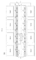
- the first semiconductor chip of the conventional stack package includes a bank unit 110 , a TSV insertion unit 120 , a pad unit 130 , and a TSV control unit 140 .
- the bank unit 110 includes a plurality of banks BANK 0 to BANK 7 for storing data.
- the TSV insertion unit 120 includes a plurality of TSVs. For stacking the chips, a TSV of a first semiconductor chip (not shown) is physically and electrically coupled to that of a second semiconductor chip (not shown).
- the pad unit 130 includes a plurality of power pads 131 , a plurality of signal pads 132 , and a plurality of probe pad 133 which are alternately arranged.
- the TSV control unit 140 is configured to control the TSV formed through the TSV insertion unit 120 .
- a selected TSV of the first semiconductor chip has to be electrically connected with a selected pad of the pad unit 130 which are formed in the first semiconductor chip. Since the TSV insertion unit 120 is arranged between the bank unit 110 and the pad unit 130 to occupy a predetermined area, the size of the semiconductor chip inevitably increases. Further, it needs a plurality of interconnection lines for connecting between the TSVs and the pads.
- a semiconductor chip comprises: a bank unit including a plurality of banks configured to store data; a pad unit including a plurality of pads arranged therein, and configured to provide external signals to the bank unit and to arranged in a pad area; and a TSV insertion unit including one or more through-silicon via, wherein the TSV insertion unit is arranged in the pad area.
- a semiconductor apparatus in which a plurality of semiconductor chips stacked in a vertical direction.
- Each of the semiconductor chips comprises: a bank area comprising a plurality of banks configured to store data; and a peripheral area including a pad area in which a plurality of pads configured to receive signals for controlling the bank area and a plurality of TSV for electrically connecting the plurality of pads, respectively.
- a method of arranging a semiconductor chip comprises: defining a bank area and a peripheral area; dividing the peripheral area into a pad area to be arranged a plurality of pads and a peripheral circuit area; forming a plurality of pads in the pad area; and forming a plurality of TSVs in the TSV insertion unit area.
- FIG. 1 is a configuration diagram illustrating a part of a first semiconductor chip of a conventional semiconductor apparatus
- FIG. 2 is a configuration diagram illustrating a part of a first semiconductor chip of a semiconductor apparatus according to an embodiment of the present invention
- FIG. 3 is a configuration diagram illustrating a part of a first semiconductor chip of a semiconductor apparatus according to another embodiment of the present invention.
- FIG. 4 is a configuration diagram illustrating a part of a first semiconductor chip of a semiconductor apparatus according to another embodiment of the present invention.
- the semiconductor apparatus that is, a semiconductor stack package according to the embodiment of the present invention may have a structure in which one or more semiconductor chips are stacked.
- a first semiconductor chip 200 may include a bank area 210 and a peripheral area 220 .
- the bank area 210 may include a plurality of banks BANK 0 to BANK 7 for storing data.
- the peripheral area 220 may include a peripheral circuit area PC to be formed a plurality of control circuits for controlling operations of the respective banks BANK 0 to BANK 7 l included in the bank area 210 and a pad area PA to be formed pads.
- the bank area 210 may have a half bank structure which may be divided into an up bank 211 and a down bank 212 based on a half line HL of the first semiconductor chip 200 or the peripheral area 220 .
- the up bank 211 and the down bank 212 may be spaced from each other with the peripheral area 220 provided there between.
- the peripheral area 220 may include a pad unit 221 , a TSV insertion unit 222 , and a TSV control unit 223 .
- the pad unit 221 may include a plurality of power pads 221 a related to power of the first semiconductor chip 200 , a plurality of signal pads 221 b configured to receive an external signal, and a plurality of probe pads 221 c configured to locally check whether a semiconductor chip has a defect or not.
- the pad unit 221 may be arranged in the pad area PA.
- the TSV insertion unit 222 may include a plurality of TSVs. The TSVs may provide external signals to circuit devices which are integrated in the first semiconductor chip 200 through the pads.
- the TSVs of the first semiconductor chip 200 may be connected to a second semiconductor chip (not shown) which is stacked on or under the first semiconductor chip, through an external connecting member, for example, bumps.
- the TSV insertion unit 221 may be formed to correspond to the up bank 211 and the down bank 212 , respectively.
- the TSV control unit 223 may be configured to control a plurality of TSVs arranged in the TSV insertion units 222 .
- the peripheral area 220 may further include a plurality of control circuits for controlling the operation of the bank area 210 , for example, a decoding block.
- the TSV insertion unit 222 may be arranged in the pad unit 221 . That is, the TSV insertion unit 222 and the pad unit 221 may be arranged in the pad area PA. For example, the TSV insertion unit 222 and the pad unit 221 may be arranged to form a substantial a same line (or row).
- the pad unit 221 may include a plurality of pads having a same function.
- an area in which the TSV insertion unit 222 will be formed may be provided.
- the removed pads may be the power pads 221 a.
- the position of the TSV insertion unit 222 may be changed depending on the position of the TSV control unit 223 .
- the TSV insertion unit 222 may be disposed at a position close to the TSV control unit 223 , in order to reduce signal loading with the TSV control unit 223 .
- FIG. 3 illustrates that the TSV insertion unit 222 corresponds to each of the up bank 211 and the down bank 212 .
- the structure is not limited thereto, but the TSV insertion unit 222 may be selectively disposed nearby the up bank 211 or the down bank 212 .
- the plurality of TSVs may be constituted of TSVs 222 a receiving GIO signals and DQ signals (for example, signals or data loaded on global input/output lines), TSVs 222 b receiving address clocks and TSVs 222 c receiving command clocks.
- the TSVs 222 may be sorted and arranged by function types, that is, signals inputted to TSVs.
- the TSV control unit 223 may include a first TSV control unit 223 a , a second TSV control unit 223 b , and a third TSV control unit 223 c .
- the first TSV control unit 223 a may be configured to control the TSVs 222 a receiving GIO signals and DQ signals.
- the second TSV control unit 223 b may be configured to control the TSVs 222 b receiving address clocks
- the third TSV control unit may be configured to control TSVs receiving the command clocks.
- the TSVs receiving the GIO signals and DQ signals may be disposed close to the first TSV control unit 223 a .
- the TSVs receiving the GIO signals and DQ signals may be disposed to face with the first TSV control unit 223 a .
- the TSVs 222 b receiving the address clocks may be disposed close to the second TSV control unit 223 b .
- the TSVs 222 b receiving the address clocks may be disposed to face with the second TSV control unit 223 b .
- the TSVs 222 c receiving the command clocks may be disposed close to the third TSV control unit 223 c .
- the TSVs 222 c receiving the address clocks may be disposed to face with the second TSV control unit 223 b.
- the divided TSV control units 223 are arranged close to the TSVs sorted by the function types, signal characteristics, such as the signal loading is improved.
- the TSV insertion unit 222 may be arranged in a central part of the pad area PA and the TSV control unit may be arranged in a central part of the pad circuit area PC to face with the TSV insertion unit 222 .
- the distance between the TSV insertion unit 222 and the TSV control unit 223 in the peripheral area 220 may be reduced.
- signal loading and interference with another global signal may occur may be reduced.
- an effective net die is improved.
Landscapes
- Engineering & Computer Science (AREA)
- Microelectronics & Electronic Packaging (AREA)
- Semiconductor Integrated Circuits (AREA)
Abstract
Description
Claims (19)
Applications Claiming Priority (2)
| Application Number | Priority Date | Filing Date | Title |
|---|---|---|---|
| KR1020130060142A KR20140139735A (en) | 2013-05-28 | 2013-05-28 | Semicondcutor apparatus |
| KR10-2013-0060142 | 2013-05-28 |
Publications (2)
| Publication Number | Publication Date |
|---|---|
| US20140353664A1 US20140353664A1 (en) | 2014-12-04 |
| US9236295B2 true US9236295B2 (en) | 2016-01-12 |
Family
ID=51984126
Family Applications (1)
| Application Number | Title | Priority Date | Filing Date |
|---|---|---|---|
| US14/013,932 Active US9236295B2 (en) | 2013-05-28 | 2013-08-29 | Semiconductor chip, semiconductor apparatus having the same and method of arranging the same |
Country Status (2)
| Country | Link |
|---|---|
| US (1) | US9236295B2 (en) |
| KR (1) | KR20140139735A (en) |
Cited By (2)
| Publication number | Priority date | Publication date | Assignee | Title |
|---|---|---|---|---|
| US20180366443A1 (en) * | 2017-06-16 | 2018-12-20 | Micron Technology, Inc. | Finer grain dynamic random access memory |
| US12477751B2 (en) * | 2022-04-14 | 2025-11-18 | Samsung Electronics Co., Ltd. | SRAM device and 3D semiconductor integrated circuit thereof |
Citations (4)
| Publication number | Priority date | Publication date | Assignee | Title |
|---|---|---|---|---|
| US20090278251A1 (en) | 2008-05-12 | 2009-11-12 | Taiwan Semiconductor Manufacturing Co., Ltd. | Pad Structure for 3D Integrated Circuit |
| US20100020583A1 (en) * | 2008-07-25 | 2010-01-28 | Kang Uk-Song | Stacked memory module and system |
| US20110156736A1 (en) * | 2009-12-28 | 2011-06-30 | Hynix Semiconductor Inc. | Semiconductor apparatus and probe test method thereof |
| US20120105093A1 (en) * | 2010-10-29 | 2012-05-03 | Hynix Semiconductor Inc. | Semiconductor apparatus and method of testing and manufacturing the same |
-
2013
- 2013-05-28 KR KR1020130060142A patent/KR20140139735A/en not_active Withdrawn
- 2013-08-29 US US14/013,932 patent/US9236295B2/en active Active
Patent Citations (4)
| Publication number | Priority date | Publication date | Assignee | Title |
|---|---|---|---|---|
| US20090278251A1 (en) | 2008-05-12 | 2009-11-12 | Taiwan Semiconductor Manufacturing Co., Ltd. | Pad Structure for 3D Integrated Circuit |
| US20100020583A1 (en) * | 2008-07-25 | 2010-01-28 | Kang Uk-Song | Stacked memory module and system |
| US20110156736A1 (en) * | 2009-12-28 | 2011-06-30 | Hynix Semiconductor Inc. | Semiconductor apparatus and probe test method thereof |
| US20120105093A1 (en) * | 2010-10-29 | 2012-05-03 | Hynix Semiconductor Inc. | Semiconductor apparatus and method of testing and manufacturing the same |
Cited By (5)
| Publication number | Priority date | Publication date | Assignee | Title |
|---|---|---|---|---|
| US20180366443A1 (en) * | 2017-06-16 | 2018-12-20 | Micron Technology, Inc. | Finer grain dynamic random access memory |
| US11527510B2 (en) * | 2017-06-16 | 2022-12-13 | Micron Technology, Inc. | Finer grain dynamic random access memory |
| US20230063029A1 (en) * | 2017-06-16 | 2023-03-02 | Micron Technology, Inc. | Finer grain dynamic random access memory |
| US11791317B2 (en) * | 2017-06-16 | 2023-10-17 | Micron Technology, Inc. | Finer grain dynamic random access memory |
| US12477751B2 (en) * | 2022-04-14 | 2025-11-18 | Samsung Electronics Co., Ltd. | SRAM device and 3D semiconductor integrated circuit thereof |
Also Published As
| Publication number | Publication date |
|---|---|
| KR20140139735A (en) | 2014-12-08 |
| US20140353664A1 (en) | 2014-12-04 |
Similar Documents
| Publication | Publication Date | Title |
|---|---|---|
| US12222880B2 (en) | Stacked semiconductor device assembly in computer system | |
| US7834450B2 (en) | Semiconductor package having memory devices stacked on logic device | |
| US7791175B2 (en) | Method for stacking serially-connected integrated circuits and multi-chip device made from same | |
| US20140048947A1 (en) | System package | |
| US20170256290A1 (en) | Stacked dram device and method of manufacture | |
| US9356000B2 (en) | Semiconductor integrated circuit and semiconductor system with the same | |
| US20110161583A1 (en) | Memory card and memory system including semiconductor chips in stacked structure | |
| US9559079B2 (en) | Semiconductor stack packages | |
| CN113012742A (en) | Semiconductor device with a plurality of semiconductor chips | |
| US20130093099A1 (en) | Semiconductor apparatus | |
| US20120049361A1 (en) | Semiconductor integrated circuit | |
| US10679956B2 (en) | Semiconductor memory chip, semiconductor memory package, and electronic system using the same | |
| JP2014071932A (en) | Multi-chip memory module | |
| US9224682B2 (en) | Semiconductor device | |
| JP6207228B2 (en) | Integrated circuit device and configuration method thereof | |
| US20120273961A1 (en) | Semiconductor apparatus | |
| US9236295B2 (en) | Semiconductor chip, semiconductor apparatus having the same and method of arranging the same | |
| JP7033332B2 (en) | Semiconductor module | |
| KR20130131548A (en) | Stacked semiconductor module | |
| KR20140028209A (en) | Semiconductor chip, semiconductor stack package having the chip and chip selection method for the same | |
| US20080116572A1 (en) | Semiconductor memory modules, methods of arranging terminals therein, and methods of using thereof | |
| KR101013565B1 (en) | Laminated Semiconductor Packages | |
| KR20110131683A (en) | Semiconductor memory device | |
| KR20110131578A (en) | Semiconductor device for efficiently supplying power to stacked memory chips | |
| US20130043601A1 (en) | Universal printed circuit board and memory card including the same |
Legal Events
| Date | Code | Title | Description |
|---|---|---|---|
| AS | Assignment |
Owner name: SK HYNIX INC., KOREA, REPUBLIC OF Free format text: ASSIGNMENT OF ASSIGNORS INTEREST;ASSIGNORS:YOON, YOUNG HEE;LEE, KANG SEOL;REEL/FRAME:031112/0832 Effective date: 20130809 |
|
| STCF | Information on status: patent grant |
Free format text: PATENTED CASE |
|
| FEPP | Fee payment procedure |
Free format text: PAYOR NUMBER ASSIGNED (ORIGINAL EVENT CODE: ASPN); ENTITY STATUS OF PATENT OWNER: LARGE ENTITY |
|
| MAFP | Maintenance fee payment |
Free format text: PAYMENT OF MAINTENANCE FEE, 4TH YEAR, LARGE ENTITY (ORIGINAL EVENT CODE: M1551); ENTITY STATUS OF PATENT OWNER: LARGE ENTITY Year of fee payment: 4 |
|
| MAFP | Maintenance fee payment |
Free format text: PAYMENT OF MAINTENANCE FEE, 8TH YEAR, LARGE ENTITY (ORIGINAL EVENT CODE: M1552); ENTITY STATUS OF PATENT OWNER: LARGE ENTITY Year of fee payment: 8 |
|
| AS | Assignment |
Owner name: MIMIRIP LLC, TEXAS Free format text: ASSIGNMENT OF ASSIGNORS INTEREST;ASSIGNOR:SK HYNIX INC.;REEL/FRAME:067335/0246 Effective date: 20240311 |