US9229164B2 - Butt-coupled buried waveguide photodetector - Google Patents
Butt-coupled buried waveguide photodetector Download PDFInfo
- Publication number
- US9229164B2 US9229164B2 US13/868,477 US201313868477A US9229164B2 US 9229164 B2 US9229164 B2 US 9229164B2 US 201313868477 A US201313868477 A US 201313868477A US 9229164 B2 US9229164 B2 US 9229164B2
- Authority
- US
- United States
- Prior art keywords
- region
- optical waveguide
- forming
- semiconductor optical
- germanium material
- Prior art date
- Legal status (The legal status is an assumption and is not a legal conclusion. Google has not performed a legal analysis and makes no representation as to the accuracy of the status listed.)
- Expired - Fee Related
Links
Images


Classifications
-
- G—PHYSICS
- G02—OPTICS
- G02B—OPTICAL ELEMENTS, SYSTEMS OR APPARATUS
- G02B6/00—Light guides; Structural details of arrangements comprising light guides and other optical elements, e.g. couplings
- G02B6/10—Light guides; Structural details of arrangements comprising light guides and other optical elements, e.g. couplings of the optical waveguide type
- G02B6/12—Light guides; Structural details of arrangements comprising light guides and other optical elements, e.g. couplings of the optical waveguide type of the integrated circuit kind
- G02B6/13—Integrated optical circuits characterised by the manufacturing method
-
- G—PHYSICS
- G02—OPTICS
- G02B—OPTICAL ELEMENTS, SYSTEMS OR APPARATUS
- G02B6/00—Light guides; Structural details of arrangements comprising light guides and other optical elements, e.g. couplings
- G02B6/10—Light guides; Structural details of arrangements comprising light guides and other optical elements, e.g. couplings of the optical waveguide type
- G02B6/12—Light guides; Structural details of arrangements comprising light guides and other optical elements, e.g. couplings of the optical waveguide type of the integrated circuit kind
- G02B6/12004—Combinations of two or more optical elements
-
- G—PHYSICS
- G02—OPTICS
- G02B—OPTICAL ELEMENTS, SYSTEMS OR APPARATUS
- G02B6/00—Light guides; Structural details of arrangements comprising light guides and other optical elements, e.g. couplings
- G02B6/10—Light guides; Structural details of arrangements comprising light guides and other optical elements, e.g. couplings of the optical waveguide type
- G02B6/12—Light guides; Structural details of arrangements comprising light guides and other optical elements, e.g. couplings of the optical waveguide type of the integrated circuit kind
- G02B6/13—Integrated optical circuits characterised by the manufacturing method
- G02B6/132—Integrated optical circuits characterised by the manufacturing method by deposition of thin films
Definitions
- the present invention generally relates to semiconductor devices, and particularly to integrated photonic semiconductor devices.
- an integrated photonic device may include both photodetector and CMOS type devices that may be fabricated on a single substrate.
- CMOS devices While engaging in the fabrication of one type of device (i.e., photonic devices); other device types (i.e., CMOS devices) may be impacted.
- CMOS devices While engaging in the fabrication of one type of device (i.e., photonic devices); other device types (i.e., CMOS devices) may be impacted.
- CMOS devices complementary metal-oxidedode-based on silicon dioxide.
- a method of forming an integrated photonic semiconductor structure having a photodetector device and a CMOS device may include forming a well region for the CMOS device, forming an isolation region for electrically isolating the photodetector device from the well region, and forming a semiconductor optical waveguide for propagating optical signals.
- germanium material is deposited adjacent to an end facet of the semiconductor optical waveguide, whereby the deposited germanium material forms an active region of the photodetector device for receiving the propagating optical signals from the end facet of the semiconductor optical waveguide structure.
- a method of forming an integrated photonic semiconductor structure having a photodetector device and a CMOS device may include forming the CMOS device on a first silicon-on-insulator region and forming a silicon optical waveguide on a second silicon-on-insulator region.
- a shallow trench isolation region surrounding the silicon optical waveguide is also formed such that the shallow trench isolation electrically isolates the first and the second silicon-on-insulator region.
- germanium material is deposited adjacent an end facet of the semiconductor optical waveguide, whereby the deposited germanium material forms an active region of the photodetector device for receiving propagating optical signals from the end facet of the semiconductor optical waveguide.
- an integrated photonic semiconductor structure may include a substrate, an isolation region, a CMOS device located on the substrate, and a semiconductor optical waveguide structure located on the substrate and electrically isolated from the CMOS device by the isolation region, whereby the semiconductor optical waveguide structure has an end facet.
- the integrated photonic semiconductor structure further includes a photodetector located within the isolation region such that the photodetector has a germanium active region located adjacent to the end facet of the waveguide structure. The germanium active region receives propagating optical signals from the end facet of the semiconductor optical waveguide.
- a design structure tangibly embodied in a machine readable medium for designing, manufacturing, or testing an integrated circuit may include a substrate, an isolation region, a CMOS device located on the substrate, and a semiconductor optical waveguide structure located on the substrate and electrically isolated from the CMOS device by the isolation region, whereby the semiconductor optical waveguide structure has an end facet.
- the integrated photonic semiconductor structure further includes a photodetector located within the isolation region such that the photodetector has a germanium active region located adjacent to the end facet of the waveguide structure. The germanium active region receives propagating optical signals from the end facet of the semiconductor optical waveguide.
- FIG. 1 is a plan view of an integrated photonic semiconductor device structure including a seed window according to an exemplary embodiment
- FIGS. 2 A- 2 J′ are cross-sectional views corresponding to the fabrication of the integrated photonic semiconductor device structure of FIG. 1 , according to an exemplary embodiment.
- FIG. 3 is a flow diagram of a design process used in semiconductor design, manufacture, and/or test according to an exemplary embodiment.
- the integrated photonic semiconductor device structure includes a butt-coupled buried waveguide photodetector device created within a shallow trench isolation (STI) region that electrically isolates the photodetector device from one or more adjacent CMOS devices.
- STI shallow trench isolation
- CMOS integrated nanophotonics device that includes, for example, both a photonic device such as a germanium (Ge) photodetector and a CMOS device such as an FET.
- a photonic device such as a germanium (Ge) photodetector
- CMOS device such as an FET.
- crystalline materials such as germanium or III-V compounds may be utilized as an active element of the photodetector component based on their high quantum efficiency.
- films e.g., germanium
- PVD physical vapor deposition
- RPCVD reduced pressure chemical vapor deposition
- PECVD plasma enhanced chemical vapor deposition
- RTCVD rapid thermal chemical vapor deposition
- a deposited amorphous state germanium film may be crystallized by heating the semiconductor wafer over which the germanium film is deposited to about 1100 degrees centigrade (° C.). At around 940° C., the germanium film transforms from a solid state to a liquid state. During a subsequent cooling stage, the liquid germanium is transformed back to a solid as a single crystalline germanium material for forming, for example, a photodetector active region.
- FIG. 1 is a plan view of an integrated photonic semiconductor device structure 100 including a seed window 102 according to one exemplary embodiment.
- a photodetector structure 104 may include a substantially rectangular region 105 formed adjacent the end facet 107 of a semiconductor waveguide structure 108 .
- an optical signal e.g., 1310 nm or 1550 nm wavelength
- the optical signal propagates within the waveguide 108 along the direction of arrow X
- the optical signal is directly coupled to the photodetector 104 via end facet 107 of the waveguide structure 108 .
- the rectangular region 105 of the photodetector 104 which forms the active region, is fabricated within STI region 114 of the integrated photonic semiconductor device structure 100 .
- active regions 116 a and 116 b may be utilized to fabricate CMOS devices such as one or more FET transistor devices (not shown), whereby the active regions 116 a , 116 b are electrically isolated from the photodetector 104 and waveguide structure 108 via the STI region 114 .
- the seed window 102 facilitates the establishment of contact between the deposited germanium film material with the silicon material of optical waveguide 108 . This contact enables the germanium film to utilize the silicon material of optical waveguide 108 as a seed layer during the crystallization process described above. Consequently, upon crystallization, the germanium active region including region 105 is formed.
- the optical waveguiding may be provided based on the waveguide structure 108 acting as a core having a first refractive index, and the surrounding STI material, as defined by C cl , functioning as a cladding having a second refractive index.
- light is internally guided within the waveguide structure 108 and subsequently directly couples to the rectangular active region 105 of the photodetector 104 .
- guided light may be efficiently received by the rectangular active region 105 of the photodetector 104 as a result of the direct coupling (i.e., butt-coupling) between the photodetector 104 and the semiconductor waveguide structure 108 .
- the footprint or size of the photodetector 104 may be reduced in favor of an increased operating speed.
- FIGS. 2 A- 2 J′ are cross-sectional views corresponding to the fabrication of the integrated photonic semiconductor device structure 100 of FIG. 1 , according to an exemplary embodiment.
- FIGS. 2 A- 2 J′ illustrate integrated photonic semiconductor device processes for forming a photonic device such as a photodetector within an STI region utilized for electrically isolating the photodetector from CMOS devices such FET transistors.
- the figures i.e., FIGS. 2 A- 2 J′
- FIGS. 2 A- 2 J′ include two cross sectional view taken along axis A-A′, and B-B′ of FIG. 1 .
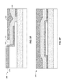
- FIG. 2A is a cross sectional view of a semiconductor structure taken across axis A-A′ of FIG. 1
- FIG. 2 A′ is a cross sectional view of the same semiconductor structure taken across axis B-B′ of FIG. 1 .
- FIG. 2A refers to a cross sectional view of integrated photonic semiconductor structure 200 taken along axis A-A′ of FIG. 1 .
- structure 200 includes a silicon (Si) substrate 202 , a buried oxide (BOX) layer 204 formed over the Si substrate 202 , and a silicon-on-insulator (SOI) region 206 corresponding to the waveguide structure 108 formed over the BOX layer 204 .
- the SOI region 206 may be utilized as an active (Rx) region for creating both photonic (e.g., silicon optical waveguides) and CMOS (e.g., FET transistor devices) type device structures.
- photonic e.g., silicon optical waveguides
- CMOS e.g., FET transistor devices
- the SOI region 206 may have a thickness, as defined by T th , of, for example, 220 nm for 1550 nm optical wavelengths and 170 nm for 1310 nm optical wavelengths.
- a silicon nitride (Si 3 N 4 ) layer 208 may be deposited over a protective oxide layer 203 formed on the SOI region 206 , whereby the nitride (Si 3 N 4 ) layer 208 may, for example, act as a polish stop during subsequent process steps.
- a thin layer of oxide 210 having a thickness of about 20-40 nm is deposited over a portion 212 of the BOX layer 204 , a portion 214 of the SOI region 206 , and over the silicon nitride layer 208 .
- Region 212 may be formed by photolithographic patterning and dry etching (e.g., RIE) of a SOI layer (not shown) located over BOX layer 204 .
- a subsequent photolithographic patterning and partial dry etching (e.g., RIE etching) process may be carried out in order to then form portion 214 of the SOI region 206 .
- portion 214 is created in the shape of a step having a thickness of about 50 nm.
- region 214 may be used to form a seed window 102 ( FIG. 1 ) for the crystallization of the deposited germanium material used to create the active region of the photodetector 104 ( FIG. 1 ).
- FIG. 2 A′ refers to a cross sectional view of integrated photonic semiconductor structure 200 taken along axis B-B′ of FIG. 1 .
- structure 200 along B-B′ also includes Si substrate 202 , BOX layer 204 formed over the Si substrate 202 , and SOI region 206 formed over the BOX layer 204 .
- oxide 210 may be deposited over region 214 of the SOI layer 206 .
- FIG. 2B refers to a cross sectional view of integrated photonic semiconductor structure 215 taken along axis A-A′ of FIG. 1 .
- the integrated photonic semiconductor structure 215 may be formed by patterned and etched anti-reflection coating 218 and photoresist layer 220 , which are deposited over integrated photonic semiconductor structure 200 ( FIG. 2A ).
- the anti-reflection coating 218 may be deposited over the structure 200 ( FIG. 2A ) to create a planar surface for receiving a photoresist layer, which is then patterned to create patterned photoresist layer 220 .
- the opening 222 in the patterned photoresist layer 220 is utilized in order to form the seed window 102 ( FIG. 1 ) described above.
- the oxide layer 210 may be etched (e.g., RIE) selective to region 228 of the SOI layer 206 with minimal overetch into region 231 of BOX layer 204 .
- RIE etching
- the dotted regions 230 , 232 of the oxide layer 210 are etched away leaving oxide liner regions 233 and 234 , which are protected by the patterned photoresist layer 220 .
- the deposited amorphous germanium material contacts silicon region 228 to produce a Ge seed layer.
- FIG. 2 B′ refers to a cross sectional view of the integrated photonic semiconductor structure 215 taken along axis B-B′ of FIG. 1 .
- the deposited anti-reflection coating 218 conformally covers oxide region 234 .
- FIG. 2C refers to a cross sectional view of integrated photonic semiconductor structure 235 taken along axis A-A′ of FIG. 1 .
- the integrated photonic semiconductor structure 235 may be formed by depositing a layer of germanium material 236 over integrated photonic semiconductor structure 215 ( FIG. 2B ) once the anti-reflection coating 218 ( FIG. 2B ) and the patterned photoresist 220 ( FIG. 2B ) layers have been stripped away.
- the Ge layer 236 may be deposited using PVD, PECVD, RTCVD, or RPCVD deposition methods. The thickness of the deposited layer of germanium material may be about 50-200 nm.
- Ge layer 236 may be formed by photolithographically patterning and etching (not shown) the integrated photonic semiconductor structure 235 in a manner that removes excess germanium material from the sidewalls S w ( FIG. 1 ) of the semiconductor waveguide structure 108 .
- FIG. 2 C′ refers to a cross sectional view of the integrated photonic semiconductor structure 235 taken along axis B-B′ of FIG. 1 .
- the deposited Ge layer 236 conformally covers the SOI region 206 .
- FIG. 2D refers to a cross sectional view of integrated photonic semiconductor structure 240 taken along axis A-A′ of FIG. 1 .
- the integrated photonic semiconductor structure 240 may be formed by depositing an undoped thick oxide fill layer 242 over the deposited Ge layer 236 of integrated photonic semiconductor structure 235 ( FIG. 2C ) using, for example, a high density plasma (HDP) deposition technique.
- the thick oxide fill 242 may act as an electrical insulating material utilized within the shallow trench isolation region 114 ( FIG. 1 ), which electrically isolates the active regions 116 a , 116 b ( FIG. 1 ), other active regions (not shown), and the waveguide structure 108 ( FIG. 1 ).
- a photodetector may be formed adjacent to the end facet 243 of the waveguide structure 108 .
- the thick oxide fill 242 e.g., SiO 2
- the thick oxide fill 242 may include a silicon dioxide (SiO 2 ) material having a thickness in the range of about 3000-6000 Angstroms ( ⁇ ).
- FIG. 2 D′ refers to a cross sectional view of the integrated photonic semiconductor structure 240 taken along axis B-B′ of FIG. 1 .
- the deposited oxide fill layer 242 conformally cover the deposited Ge layer 236 located over the oxide liner region 234 .
- FIG. 2E refers to a cross sectional view of integrated photonic semiconductor structure 245 taken along axis A-A′ of FIG. 1 .
- the integrated photonic semiconductor structure 245 may be formed by planarizing integrated photonic semiconductor structure 240 using chemical mechanical polishing (CMP). As depicted, the entire oxide fill 242 ( FIG. 2D ), the Ge layer 236 ( FIG. 2D ), and the oxide liner 234 ( FIG. 2D ) located above silicon nitride layer 208 is removed. During the CMP process, approximately 10-20% of the silicon nitride layer 208 may also be removed in order to ensure that no residual material remains on the surface of the silicon nitride layer 208 . Also, region 241 ( FIG.
- oxide fill 266 , oxide liner 268 , and Ge layer 248 adjacent the silicon nitride layer 208 may be recessed to about 50% of the thickness t sn of the silicon nitride layer 208 .
- FIG. 2 E′ refers to a cross sectional view of the integrated photonic semiconductor structure 245 taken along axis B-B′ of FIG. 1 . As depicted, following the CMP process, a portion 269 of the oxide fill region 269 (FIG. 2 D′) is removed.
- FIG. 2F refers to a cross sectional view of integrated photonic semiconductor structure 270 taken along axis A-A′ of FIG. 1 .
- the integrated photonic semiconductor structure 270 may be formed by creating recess region 272 .
- Recess region 272 may be formed by etching (e.g., RIE etch) portion 273 ( FIG. 2E ) of Ge region 248 ( FIG. 2E ) corresponding to integrated photonic semiconductor structure 245 ( FIG. 2E ).
- the exposed surface S Ge of the Ge region 248 may be subjected to chemical attack during subsequent processing steps that may use, for example, various cleaning agents and acids.
- the formed recess region 272 depicted in FIG. 2F is utilized to form a plug (see FIG. 2G ) that encapsulates the Ge region 248 for protection during the subsequent processing of the integrated photonic semiconductor structure 270 .
- FIG. 2 F′ refers to a cross sectional view of the integrated photonic semiconductor structure 270 taken along axis B-B′ of FIG. 1 . As depicted, FIG. 2 F′ remains identical with that of FIG. 2 E′, whereby, following the CMP process, portion 269 (FIG. 2 D′) of the oxide fill region 242 (FIG. 2 D′) is removed.
- FIG. 2G refers to a cross sectional view of integrated photonic semiconductor structure 275 taken along axis A-A′ of FIG. 1 .
- FIG. 2 G′ refers to a cross sectional view of integrated photonic semiconductor structure 275 taken along axis B-B′ of FIG. 1 .
- the integrated photonic semiconductor structure 275 may be formed by filling recess region 272 (also see FIG. 2F ) with silicon nitride fill material 279 (i.e., a silicon nitride plug).
- FIG. 2 G′ also shows the deposited silicon nitride fill material 279 .
- Ge region 248 is now encapsulated and, thus, protected by the deposited silicon nitride fill material 279 .
- FIG. 2H refers to a cross sectional view of integrated photonic semiconductor structure 280 taken along axis A-A′ of FIG. 1 .
- the integrated photonic semiconductor structure 280 may be formed by stripping, using hot phosphoric acid (H 3 PO 4 ), silicon nitride material layer 208 ( FIG. 2G ) and the entire silicon nitride fill material 279 ( FIG. 2G ) located over the oxide fill layer 266 .
- silicon nitride plug 282 remains over, and facilitates, the encapsulation of Ge region 248 in order to, as previously described, protect the germanium material from subsequent fabrication processes such as cleans.
- the slow etch rate of oxide layer 203 protects the underlying SOI region 206 during the hot phosphoric acid (H 3 PO 4 ) stripping of silicon nitride layer 208 ( FIG. 2G ).
- FIG. 2 H′ refers to a cross sectional view of integrated photonic semiconductor structure 280 taken along axis B-B′ of FIG. 1 .
- the nitride stripping process removes silicon nitride fill material 279 (FIG. 2 G′).
- FIG. 2I refers to a cross sectional view of integrated photonic semiconductor structure 290 taken along axis A-A of FIG. 1 .
- FET transistor 291 may be formed adjacent photodetector region 294 within an SOI region of another active region 116 c ( FIG. 1 ) separated by STI region 114 (also see FIG. 1 ).
- dopant implants e.g., phosphorus for N-well regions and boron for P-well regions
- a well region 292 FIG. 2I
- CMOS device such as an FET 291 .
- a thermal anneal process may be carried out for simultaneously initiating both the activation of the well dopants within the well region 292 and the crystallization of the germanium region 248 ( FIG. 2H ) that forms photodetector active region 249 a .
- the thermal anneal process may include heating integrated photonic semiconductor structure 290 to a temperature of about 1030° C. for a period of approximately 5 seconds.
- the crystallization of the Ge region 248 ( FIG. 2H ) and forming active region 249 a is accomplished via seed window 102 ( FIG. 2H ), whereby the germanium material at region 249 ( FIG. 2H ) contacts the silicon material of SOI layer 206 at surface S SOI ( FIG. 2H ) for facilitating such crystallization.
- region 251 is patterned and etched in order to remove both germanium material from region 251 ( FIG. 2H ) and oxide fill 266 ( FIG. 2H ).
- This germanium material is etched away in order to remove the germanium seed window 102 ( FIG. 2H ) that was used in the crystallization process.
- subsequent process steps may cause recrystallization of the germanium region 248 ( FIG. 2H ), which causes the formation of a polycrystalline germanium material.
- the formed polycrystalline germanium material may adversely affect the photodetection performance by, for example, reducing the photodetector's responsivity. Thus, recrystallization is eliminated by removing the seed window as described.
- both the germanium 248 and oxide fill 266 are etched selective to the SOI region 206 .
- Oxide region 233 remains intact.
- the etch process may be carried-out in two stages, whereby, firstly the oxide fill 266 within region 251 is etched, followed by the germanium 248 within region 251 .
- the etched region may be filled with 1000-2000 ⁇ of, for example, spacer oxide or spacer nitride material, which may be deposited during the formation of spacers for the CMOS FET transistor 291 .
- CMOS FET transistor 291 is formed adjacent to the photodetector region 294 via STI isolation region 114 .
- the photodetector region 294 includes Ge active region 249 a , whereby the Ge active region 249 a is formed adjacent the end facet 243 of optical waveguide 108 .
- FIG. 1 depicted exemplary embodiment of FIG.
- the formed CMOS FET transistor 291 may include a gate dielectric 213 , a polysilicon gate electrode 217 , spacer oxide regions 219 , spacer nitride regions 221 , source/drain (S/D) regions 294 a , 294 b , and halo and extension implants (not shown).
- Well region 292 and the S/D regions 294 a , 294 b of FET transistor 291 may be formed within active region 116 c ( FIG. 1 ) of silicon-on-insulator (SOI) layer 207 ( FIG. 1 ).
- a lithographically patterned and etched layer of silicon nitride may be formed over the photodetector region 294 having Ge active region 249 a .
- the patterned layer of silicon nitride may serve to further protect the photodetector active region 249 a during the formation of respective silicide regions 298 a , 298 b , and 298 c on the S/D regions 294 a , 294 b and the gate electrode 217 .
- the photodetector active region 249 a is encapsulated by silicon nitride plug 282 , oxide liner 234 , oxide layer 255 , and silicon dioxide/silicon nitride fill material 254 .
- An optical signal as denoted by O sig , is guided along waveguide structure 108 , and coupled to the photodetector active region 249 a via the oxide liner 234 located between the active region 249 a and the end facet 243 of waveguide 108 .
- oxide liner 234 may be about 20 ⁇ -40 ⁇ , although greater or lesser thickness values may also be contemplated.
- the presence of the oxide liner 234 between the end facet 243 of the waveguide 108 and the active region 249 a inhibits any direct contact between the germanium material of the active region 249 a and the silicon material of the waveguide 108 .
- the active region 249 a of the photodetector abuts the end facet 243 of the waveguide 108 via the thin oxide liner 234 and, therefore, receives substantially the entire optical signal O sig propagating within the waveguide 108 and incident on the end facet 243 of the waveguide 108 .
- the geometric size of the photodetector and, therefore, the active region 249 a area may be reduced. By reducing the size of the photodetector's active region 249 a area, less device capacitance and higher operational speeds may be achieved.
- FET transistor 291 is illustrated as an adjacent device to the photodetector region 294 , it may be appreciated that multiple other adjacent transistor devices can be fabricated within other active regions surrounding the photodetector region 294 , such as, for example, active regions 116 a ( FIG. 1) and 116 b ( FIG. 1 ). In some implementations, one or more FETs may be electrically connected to one or more photodetectors in order to form optical receiver circuitry.
- FIG. 2 I′ refers to a cross sectional view of integrated photonic semiconductor structure 290 taken along axis B-B′ of FIG. 1 .
- the prior nitride stripping process removed silicon nitride fill material 279 (FIG. 2 G′).
- FIG. 2J refers to a cross sectional view of integrated photonic semiconductor structure 295 taken along axis B-B′ of FIG. 1 .
- Integrated photonic semiconductor structure 295 may be formed by creating electrical contacts for the photodetector region 294 and CMOS FET transistor 291 of integrated photonic semiconductor structure 290 ( FIG. 2I ).
- integrated photonic semiconductor structure 295 may be formed by depositing an interlayer dielectric material 223 over integrated photonic semiconductor structure 290 ( FIG. 2I ).
- the interlayer dielectric material 223 may, for example, include 5000-10,000 ⁇ of BPSG material.
- the contacts 299 a - 299 f may be formed by etching into the interlayer dielectric 223 .
- contacts 299 a - 299 c establish electrically conductive connections with Ge active region 249 a of photodetector region 294
- contact 299 d establishes an electrically conductive connection with silicide region 298 a of S/D region 294 a
- contact 299 e establishes an electrically conductive connection with gate silicide region 298 c
- contact 299 f establishes an electrically conductive connection with silicide region 298 b of S/D region 294 b.
- FIG. 2 J′ refers to a cross sectional view of integrated photonic semiconductor structure 295 taken along axis B-B′ of FIG. 1 .
- contacts 299 a - 299 c establish electrically conductive connections with Ge active region 249 a of photodetector region 294 .
- FIG. 3 shows a block diagram of an exemplary design flow 900 used for example, in semiconductor IC logic design, simulation, test, layout, and manufacture.
- Design flow 900 includes processes and mechanisms for processing design structures or devices to generate logically or otherwise functionally equivalent representations of the design structures and/or devices described above and shown in FIG. 2J .
- the design structure processed and/or generated by design flow 900 may be encoded on machine-readable transmission or storage media to include data and/or instructions that when executed or otherwise processed on a data processing system generate a logically, structurally, mechanically, or otherwise functionally equivalent representation of hardware components, circuits, devices, or systems.
- Design flow 900 may vary depending on the type of representation being designed. For example, a design flow 900 for building an application specific IC (ASIC) may differ from a design flow 900 for designing a standard component or from a design flow 900 for instantiating the design into a programmable array, for example a programmable gate array (PGA) or a field programmable gate array (FPGA) offered by Altera® Inc. or Xilinx® Inc.
- ASIC application specific IC
- PGA programmable gate array
- FPGA field programmable gate array
- FIG. 3 illustrates multiple such design structures including an input design structure 920 that is preferably processed by a design process 910 .
- the design structure 920 comprises design data used in a design process and comprising information describing the embodiments of the invention with respect to the structure as shown in FIG. 2J .
- the design data in the form of schematics or HDL, a hardware-description language (e.g., Verilog, VHDL, C, etc.) may be embodied on one or more machine readable media.
- design structure 920 may be a text file, numerical data or a graphical representation of the embodiment of the invention shown in FIG. 2J .
- Design structure 920 may be a logical simulation design structure generated and processed by design process 910 to produce a logically equivalent functional representation of a hardware device.
- Design structure 920 may also or alternatively comprise data and/or program instructions that when processed by design process 910 , generate a functional representation of the physical structure of a hardware device. Whether representing functional and/or structural design features, design structure 920 may be generated using electronic computer-aided design (ECAD) such as implemented by a core developer/designer.
- ECAD electronic computer-aided design
- design structure 920 When encoded on a machine-readable data transmission, gate array, or storage medium, design structure 920 may be accessed and processed by one or more hardware and/or software modules within design process 910 to simulate or otherwise functionally represent an electronic component, circuit, electronic or logic module, apparatus, device, or system such as that shown in FIG. 2J .
- design structure 920 may comprise files or other data structures including human and/or machine-readable source code, compiled structures, and computer-executable code structures that when processed by a design or simulation data processing system, functionally simulate or otherwise represent circuits or other levels of hardware logic design.
- Such data structures may include hardware-description language (HDL) design entities or other data structures conforming to and/or compatible with lower-level HDL design languages such as Verilog and VHDL, and/or higher level design languages such as C or C++.
- HDL hardware-description language
- Design process 910 preferably employs and incorporates hardware and/or software modules for synthesizing, translating, or otherwise processing a design/simulation functional equivalent of the components, circuits, devices, or logic structure shown in FIG. 2J to generate a netlist 980 which may contain a design structure such as design structure 920 .
- Netlist 980 may comprise, for example, compiled or otherwise processed data structures representing a list of wires, discrete components, logic gates, control circuits, I/O devices, models, etc. that describes the connections to other elements and circuits in an integrated circuit design.
- Netlist 980 may be synthesized using an iterative process in which netlist 980 is resynthesized one or more times depending on design specifications and parameters for the device.
- netlist 980 may be recorded on a machine-readable data storage medium or programmed into a programmable gate array.
- the medium may be a non-volatile storage medium such as a magnetic or optical disk drive, a programmable gate array, a compact flash, or other flash memory. Additionally, or in the alternative, the medium may be a system or cache memory, buffer space, or electrically or optically conductive devices and materials on which data packets may be transmitted and intermediately stored via the Internet, or other networking suitable means.
- Design process 910 may include hardware and software modules for processing a variety of input data structure types including netlist 980 .
- data structure types may reside, for example, within library elements 930 and include a set of commonly used elements, circuits, and devices, including models, layouts, and symbolic representations, for a given manufacturing technology (e.g., different technology nodes, 20, 32 nm, 45 nm, 90 nm, etc.).
- the data structure types may further include design specifications 940 , characterization data 950 , verification data 960 , design rules 970 , and test data files 985 which may include input test patterns, output test results, and other testing information.
- Design process 910 may further include, for example, standard mechanical design processes such as stress analysis, thermal analysis, mechanical event simulation, process simulation for operations such as casting, molding, and die press forming, etc.
- standard mechanical design processes such as stress analysis, thermal analysis, mechanical event simulation, process simulation for operations such as casting, molding, and die press forming, etc.
- One of ordinary skill in the art of mechanical design can appreciate the extent of possible mechanical design tools and applications used in design process 910 without deviating from the scope and spirit of the invention.
- Design process 910 may also include modules for performing standard circuit design processes such as timing analysis, verification, design rule checking, place and route operations, etc.
- Design process 910 employs and incorporates logic and physical design tools such as HDL compilers and simulation model build tools to process design structure 920 together with some or all of the depicted supporting data structures along with any additional mechanical design or data (if applicable), to generate a second design structure 990 comprising second design data embodied on a storage medium in a data format used for the exchange of layout data of integrated circuits and/or symbolic data format (e.g. information stored in a GDSII (GDS2), GL1, OASIS, map files, or any other suitable format for storing such design structures).
- the second design data resides on a storage medium or programmable gate array in a data format used for the exchange of data of mechanical devices and structures (e.g.
- design structure 990 preferably comprises one or more files, data structures, or other computer-encoded data or instructions that reside on transmission or data storage media and that when processed by an ECAD system generate a logically or otherwise functionally equivalent form of the embodiment of the invention shown in FIG. 2J .
- design structure 990 may comprise a compiled, executable HDL simulation model that functionally simulates the device shown in FIG. 2J .
- Design structure 990 may also employ a data format used for the exchange of layout data of integrated circuits and/or symbolic data format (e.g. information stored in a GDSII (GDS2), GL1, OASIS, map files, or any other suitable format for storing such design data structures).
- GDSII GDS2
- GL1 GL1, OASIS, map files, or any other suitable format for storing such design data structures.
- Design structure 990 may comprise information such as, for example, symbolic data, map files, test data files, design content files, manufacturing data, layout parameters, wires, levels of metal, vias, shapes, data for routing through the manufacturing line, and any other data required by a manufacturer or other designer/developer to produce a device or structure as described above and shown in FIG. 2J .
- Design structure 990 may then proceed to a stage 995 where, for example, design structure 990 : proceeds to tape-out, is released to manufacturing, is released to a mask house, is sent to another design house, is sent back to the customer, etc.
Landscapes
- Physics & Mathematics (AREA)
- Engineering & Computer Science (AREA)
- Microelectronics & Electronic Packaging (AREA)
- General Physics & Mathematics (AREA)
- Optics & Photonics (AREA)
- Optical Integrated Circuits (AREA)
- Manufacturing & Machinery (AREA)
- Metal-Oxide And Bipolar Metal-Oxide Semiconductor Integrated Circuits (AREA)
- Light Receiving Elements (AREA)
Abstract
Description
Claims (19)
Priority Applications (2)
| Application Number | Priority Date | Filing Date | Title |
|---|---|---|---|
| US13/868,477 US9229164B2 (en) | 2013-04-23 | 2013-04-23 | Butt-coupled buried waveguide photodetector |
| CN201410163915.4A CN104124304B (en) | 2013-04-23 | 2014-04-23 | Butt-coupling bury Waveguide electric explorer underground |
Applications Claiming Priority (1)
| Application Number | Priority Date | Filing Date | Title |
|---|---|---|---|
| US13/868,477 US9229164B2 (en) | 2013-04-23 | 2013-04-23 | Butt-coupled buried waveguide photodetector |
Publications (2)
| Publication Number | Publication Date |
|---|---|
| US20140312443A1 US20140312443A1 (en) | 2014-10-23 |
| US9229164B2 true US9229164B2 (en) | 2016-01-05 |
Family
ID=51728395
Family Applications (1)
| Application Number | Title | Priority Date | Filing Date |
|---|---|---|---|
| US13/868,477 Expired - Fee Related US9229164B2 (en) | 2013-04-23 | 2013-04-23 | Butt-coupled buried waveguide photodetector |
Country Status (2)
| Country | Link |
|---|---|
| US (1) | US9229164B2 (en) |
| CN (1) | CN104124304B (en) |
Cited By (5)
| Publication number | Priority date | Publication date | Assignee | Title |
|---|---|---|---|---|
| US20150303229A1 (en) * | 2013-08-20 | 2015-10-22 | International Business Machines Corporation | Cmos protection during germanium photodetector processing |
| US10830968B2 (en) | 2018-04-12 | 2020-11-10 | Samsung Electronics Co., Ltd. | Photodetector structure |
| US10910503B1 (en) | 2019-08-19 | 2021-02-02 | Globalfoundries Inc. | Semiconductor detectors with butt-end coupled waveguide and method of forming the same |
| US11075307B2 (en) | 2019-07-18 | 2021-07-27 | International Business Machines Corporation | Compact electro-optical devices with laterally grown contact layers |
| US11495700B2 (en) | 2020-02-23 | 2022-11-08 | Globalfoundries U.S. Inc. | Photodetectors and semiconductor devices |
Families Citing this family (11)
| Publication number | Priority date | Publication date | Assignee | Title |
|---|---|---|---|---|
| US9117946B2 (en) | 2013-01-15 | 2015-08-25 | International Business Machines Corporation | Buried waveguide photodetector |
| US9229164B2 (en) | 2013-04-23 | 2016-01-05 | Globalfoundries Inc. | Butt-coupled buried waveguide photodetector |
| KR102124207B1 (en) * | 2013-06-03 | 2020-06-18 | 삼성전자주식회사 | Semiconductor device and method for forming the same |
| FR3015114B1 (en) * | 2013-12-13 | 2016-01-01 | Commissariat Energie Atomique | METHOD FOR MANUFACTURING A PHOTO-DETECTOR |
| US9678273B2 (en) * | 2015-06-01 | 2017-06-13 | International Business Machines Corporation | Device for propagating light and method for fabricating a device |
| US9658400B2 (en) | 2015-06-01 | 2017-05-23 | International Business Machines Corporation | Method for fabricating a device for propagating light |
| US9466753B1 (en) | 2015-08-27 | 2016-10-11 | Globalfoundries Inc. | Photodetector methods and photodetector structures |
| US10103280B1 (en) * | 2017-04-13 | 2018-10-16 | International Business Machines Corporation | Rapid melt growth photodetector |
| US11215753B2 (en) | 2020-02-27 | 2022-01-04 | Taiwan Semiconductor Manufacturing Company, Ltd. | Photonic semiconductor device and method |
| WO2022071861A1 (en) * | 2020-10-01 | 2022-04-07 | Fingerprint Cards Anacatum Ip Ab | A biometric imaging arrangement for infrared imaging comprising a waveguide formed on an image sensor |
| US11353651B2 (en) * | 2020-11-02 | 2022-06-07 | Globalfoundries U.S. Inc. | Multi-mode optical waveguide structures with isolated absorbers |
Citations (16)
| Publication number | Priority date | Publication date | Assignee | Title |
|---|---|---|---|---|
| US6307242B1 (en) | 1998-02-19 | 2001-10-23 | Nec Corporation | Semiconductor photo-detector with square-shaped optical wave-guide |
| US6897498B2 (en) | 2003-03-31 | 2005-05-24 | Sioptical, Inc. | Polycrystalline germanium-based waveguide detector integrated on a thin silicon-on-insulator (SOI) platform |
| US7151881B2 (en) | 2003-05-29 | 2006-12-19 | Applied Materials, Inc. | Impurity-based waveguide detectors |
| US20070170536A1 (en) | 2006-01-25 | 2007-07-26 | Sharp Laboratories Of America, Inc. | Liquid phase epitaxial GOI photodiode with buried high resistivity germanium layer |
| US20070189688A1 (en) * | 2006-02-15 | 2007-08-16 | Gabriel Dehlinger | Waveguide photodetector |
| WO2008080428A1 (en) | 2006-12-29 | 2008-07-10 | Pgt Photonics S.P.A. | Waveguide photodetector in germanium on silicon |
| US7418166B1 (en) | 2006-02-24 | 2008-08-26 | The Board Of Trustees Of The Leland Stanford Junior University | Device and approach for integration of optical devices and waveguides therefor |
| US7453132B1 (en) | 2002-06-19 | 2008-11-18 | Luxtera Inc. | Waveguide photodetector with integrated electronics |
| US20090101909A1 (en) * | 2007-10-17 | 2009-04-23 | Nano Photonics, Inc. | Semiconductor photodetectors |
| US7749876B2 (en) | 2002-09-20 | 2010-07-06 | Infineon Technologies Ag | Method for the production of a buried stop zone in a semiconductor component and semiconductor component comprising a buried stop zone |
| US20100327381A1 (en) | 2009-06-30 | 2010-12-30 | Morse Michael T | Sidewall photodetector |
| US20110037133A1 (en) * | 2009-08-17 | 2011-02-17 | Tzung-I Su | Semiconductor Photodetector Structure and the Fabrication Method Thereof |
| US20110049660A1 (en) | 2009-08-31 | 2011-03-03 | Electronics And Telecommunications Research Institute | Waveguide photo-detector |
| US20120129302A1 (en) * | 2010-11-22 | 2012-05-24 | International Business Machines Corporation | Fabricating photonics devices fully integrated into a cmos manufacturing process |
| US20140197507A1 (en) * | 2013-01-15 | 2014-07-17 | International Business Machines Corporation | Buried waveguide photodetector |
| CN104124304A (en) | 2013-04-23 | 2014-10-29 | 国际商业机器公司 | Butt-coupled buried waveguide photodetector |
Family Cites Families (1)
| Publication number | Priority date | Publication date | Assignee | Title |
|---|---|---|---|---|
| CN102944912B (en) * | 2012-11-22 | 2014-04-23 | 中国科学院半导体研究所 | A SOI-based three-dimensional cross waveguide and its manufacturing method |
-
2013
- 2013-04-23 US US13/868,477 patent/US9229164B2/en not_active Expired - Fee Related
-
2014
- 2014-04-23 CN CN201410163915.4A patent/CN104124304B/en not_active Expired - Fee Related
Patent Citations (19)
| Publication number | Priority date | Publication date | Assignee | Title |
|---|---|---|---|---|
| US6307242B1 (en) | 1998-02-19 | 2001-10-23 | Nec Corporation | Semiconductor photo-detector with square-shaped optical wave-guide |
| US7453132B1 (en) | 2002-06-19 | 2008-11-18 | Luxtera Inc. | Waveguide photodetector with integrated electronics |
| US7616904B1 (en) | 2002-06-19 | 2009-11-10 | Luxtera, Inc. | Waveguide photodetector with integrated electronics |
| US7749876B2 (en) | 2002-09-20 | 2010-07-06 | Infineon Technologies Ag | Method for the production of a buried stop zone in a semiconductor component and semiconductor component comprising a buried stop zone |
| US6897498B2 (en) | 2003-03-31 | 2005-05-24 | Sioptical, Inc. | Polycrystalline germanium-based waveguide detector integrated on a thin silicon-on-insulator (SOI) platform |
| US7151881B2 (en) | 2003-05-29 | 2006-12-19 | Applied Materials, Inc. | Impurity-based waveguide detectors |
| US20070170536A1 (en) | 2006-01-25 | 2007-07-26 | Sharp Laboratories Of America, Inc. | Liquid phase epitaxial GOI photodiode with buried high resistivity germanium layer |
| US20070189688A1 (en) * | 2006-02-15 | 2007-08-16 | Gabriel Dehlinger | Waveguide photodetector |
| US7418166B1 (en) | 2006-02-24 | 2008-08-26 | The Board Of Trustees Of The Leland Stanford Junior University | Device and approach for integration of optical devices and waveguides therefor |
| WO2008080428A1 (en) | 2006-12-29 | 2008-07-10 | Pgt Photonics S.P.A. | Waveguide photodetector in germanium on silicon |
| US20090101909A1 (en) * | 2007-10-17 | 2009-04-23 | Nano Photonics, Inc. | Semiconductor photodetectors |
| US20100327381A1 (en) | 2009-06-30 | 2010-12-30 | Morse Michael T | Sidewall photodetector |
| US20110037133A1 (en) * | 2009-08-17 | 2011-02-17 | Tzung-I Su | Semiconductor Photodetector Structure and the Fabrication Method Thereof |
| US20110049660A1 (en) | 2009-08-31 | 2011-03-03 | Electronics And Telecommunications Research Institute | Waveguide photo-detector |
| US20120129302A1 (en) * | 2010-11-22 | 2012-05-24 | International Business Machines Corporation | Fabricating photonics devices fully integrated into a cmos manufacturing process |
| US8633067B2 (en) | 2010-11-22 | 2014-01-21 | International Business Machines Corporation | Fabricating photonics devices fully integrated into a CMOS manufacturing process |
| US20140197507A1 (en) * | 2013-01-15 | 2014-07-17 | International Business Machines Corporation | Buried waveguide photodetector |
| WO2014113440A1 (en) | 2013-01-15 | 2014-07-24 | International Business Machines Corporation | Buried waveguide photodetector |
| CN104124304A (en) | 2013-04-23 | 2014-10-29 | 国际商业机器公司 | Butt-coupled buried waveguide photodetector |
Non-Patent Citations (4)
| Title |
|---|
| Cervantes-Gonzalez et al., "Germanium metal-semiconductor-metal photodetectors evanescently coupled with upper-level silicon oxynitride dielectric waveguides," Applied Physics Letters, Dec. 28, 2012, vol. 101, Issue 261109, American Institute of Physics. |
| European Patent Office, "Notification of Transmittal of the International Search Report and the Written Opinion of the International Searching Authority, or the Declaration," May 27, 2014, International Application No. PCT/US2014/011629. |
| Masini et al., "Near-infared waveguide photodetectors based on polycrystalline Ge on silicon-on-insulator substrates," Optical Materials, May 30, 2000, p. 243-246, vol. 17, Elsevier Science B.V. |
| Pending U.S. Appl. No. 13/741,416, filed Jan. 15, 2013, Entitled: "Buried Waveguide Photodetector". |
Cited By (7)
| Publication number | Priority date | Publication date | Assignee | Title |
|---|---|---|---|---|
| US20150303229A1 (en) * | 2013-08-20 | 2015-10-22 | International Business Machines Corporation | Cmos protection during germanium photodetector processing |
| US9590001B2 (en) * | 2013-08-20 | 2017-03-07 | Globalfoundries Inc. | CMOS protection during germanium photodetector processing |
| US10830968B2 (en) | 2018-04-12 | 2020-11-10 | Samsung Electronics Co., Ltd. | Photodetector structure |
| US11428877B2 (en) | 2018-04-12 | 2022-08-30 | Samsung Electronics Co., Ltd. | Photodetector structure |
| US11075307B2 (en) | 2019-07-18 | 2021-07-27 | International Business Machines Corporation | Compact electro-optical devices with laterally grown contact layers |
| US10910503B1 (en) | 2019-08-19 | 2021-02-02 | Globalfoundries Inc. | Semiconductor detectors with butt-end coupled waveguide and method of forming the same |
| US11495700B2 (en) | 2020-02-23 | 2022-11-08 | Globalfoundries U.S. Inc. | Photodetectors and semiconductor devices |
Also Published As
| Publication number | Publication date |
|---|---|
| CN104124304A (en) | 2014-10-29 |
| CN104124304B (en) | 2016-08-31 |
| US20140312443A1 (en) | 2014-10-23 |
Similar Documents
| Publication | Publication Date | Title |
|---|---|---|
| US9229164B2 (en) | Butt-coupled buried waveguide photodetector | |
| US9117946B2 (en) | Buried waveguide photodetector | |
| US9036959B2 (en) | Intergrating a silicon photonics photodetector with CMOS devices | |
| US8765536B2 (en) | Stress engineered multi-layers for integration of CMOS and Si nanophotonics | |
| US11164980B2 (en) | Silicon photonics integration method and structure | |
| US10622496B2 (en) | Integrated photodetector waveguide structure with alignment tolerance | |
| US7109051B2 (en) | Method of integrating optical devices and electronic devices on an integrated circuit | |
| US9590001B2 (en) | CMOS protection during germanium photodetector processing |
Legal Events
| Date | Code | Title | Description |
|---|---|---|---|
| AS | Assignment |
Owner name: INTERNATIONAL BUSINESS MACHINES CORPORATION, NEW Y Free format text: ASSIGNMENT OF ASSIGNORS INTEREST;ASSIGNORS:ASSEFA, SOLOMON;GREEN, WILLIAM M.;SHANK, STEVEN M.;AND OTHERS;SIGNING DATES FROM 20130418 TO 20130423;REEL/FRAME:030267/0162 |
|
| AS | Assignment |
Owner name: GLOBALFOUNDRIES U.S. 2 LLC, NEW YORK Free format text: ASSIGNMENT OF ASSIGNORS INTEREST;ASSIGNOR:INTERNATIONAL BUSINESS MACHINES CORPORATION;REEL/FRAME:036550/0001 Effective date: 20150629 |
|
| AS | Assignment |
Owner name: GLOBALFOUNDRIES INC., CAYMAN ISLANDS Free format text: ASSIGNMENT OF ASSIGNORS INTEREST;ASSIGNORS:GLOBALFOUNDRIES U.S. 2 LLC;GLOBALFOUNDRIES U.S. INC.;REEL/FRAME:036779/0001 Effective date: 20150910 |
|
| STCF | Information on status: patent grant |
Free format text: PATENTED CASE |
|
| AS | Assignment |
Owner name: WILMINGTON TRUST, NATIONAL ASSOCIATION, DELAWARE Free format text: SECURITY AGREEMENT;ASSIGNOR:GLOBALFOUNDRIES INC.;REEL/FRAME:049490/0001 Effective date: 20181127 |
|
| FEPP | Fee payment procedure |
Free format text: MAINTENANCE FEE REMINDER MAILED (ORIGINAL EVENT CODE: REM.); ENTITY STATUS OF PATENT OWNER: LARGE ENTITY |
|
| LAPS | Lapse for failure to pay maintenance fees |
Free format text: PATENT EXPIRED FOR FAILURE TO PAY MAINTENANCE FEES (ORIGINAL EVENT CODE: EXP.); ENTITY STATUS OF PATENT OWNER: LARGE ENTITY |
|
| STCH | Information on status: patent discontinuation |
Free format text: PATENT EXPIRED DUE TO NONPAYMENT OF MAINTENANCE FEES UNDER 37 CFR 1.362 |
|
| FP | Lapsed due to failure to pay maintenance fee |
Effective date: 20200105 |
|
| AS | Assignment |
Owner name: GLOBALFOUNDRIES INC., CAYMAN ISLANDS Free format text: RELEASE BY SECURED PARTY;ASSIGNOR:WILMINGTON TRUST, NATIONAL ASSOCIATION;REEL/FRAME:054636/0001 Effective date: 20201117 |
|
| AS | Assignment |
Owner name: GLOBALFOUNDRIES U.S. INC., NEW YORK Free format text: RELEASE BY SECURED PARTY;ASSIGNOR:WILMINGTON TRUST, NATIONAL ASSOCIATION;REEL/FRAME:056987/0001 Effective date: 20201117 Owner name: GLOBALFOUNDRIES U.S. INC., NEW YORK Free format text: RELEASE OF SECURITY INTEREST;ASSIGNOR:WILMINGTON TRUST, NATIONAL ASSOCIATION;REEL/FRAME:056987/0001 Effective date: 20201117 |