US9222977B2 - Semiconductor test system and method - Google Patents

Semiconductor test system and method Download PDF

Info

Publication number
US9222977B2
US9222977B2 US14/807,214 US201514807214A US9222977B2 US 9222977 B2 US9222977 B2 US 9222977B2 US 201514807214 A US201514807214 A US 201514807214A US 9222977 B2 US9222977 B2 US 9222977B2
Authority
US
United States
Prior art keywords
output
input
die
test
scan
Prior art date
Legal status (The legal status is an assumption and is not a legal conclusion. Google has not performed a legal analysis and makes no representation as to the accuracy of the status listed.)
Expired - Fee Related
Application number
US14/807,214
Other versions
US20150323601A1 (en
Inventor
Lee D. Whetsel
Current Assignee (The listed assignees may be inaccurate. Google has not performed a legal analysis and makes no representation or warranty as to the accuracy of the list.)
Texas Instruments Inc
Original Assignee
Texas Instruments Inc
Priority date (The priority date is an assumption and is not a legal conclusion. Google has not performed a legal analysis and makes no representation as to the accuracy of the date listed.)
Filing date
Publication date
Priority claimed from US13/870,238 external-priority patent/US8572446B2/en
Application filed by Texas Instruments Inc filed Critical Texas Instruments Inc
Priority to US14/807,214 priority Critical patent/US9222977B2/en
Publication of US20150323601A1 publication Critical patent/US20150323601A1/en
Priority to US14/944,903 priority patent/US9417283B2/en
Application granted granted Critical
Publication of US9222977B2 publication Critical patent/US9222977B2/en
Anticipated expiration legal-status Critical
Expired - Fee Related legal-status Critical Current

Links

Images

Classifications

    • GPHYSICS
    • G01MEASURING; TESTING
    • G01RMEASURING ELECTRIC VARIABLES; MEASURING MAGNETIC VARIABLES
    • G01R31/00Arrangements for testing electric properties; Arrangements for locating electric faults; Arrangements for electrical testing characterised by what is being tested not provided for elsewhere
    • G01R31/28Testing of electronic circuits, e.g. by signal tracer
    • G01R31/317Testing of digital circuits
    • G01R31/3177Testing of logic operation, e.g. by logic analysers
    • GPHYSICS
    • G01MEASURING; TESTING
    • G01RMEASURING ELECTRIC VARIABLES; MEASURING MAGNETIC VARIABLES
    • G01R31/00Arrangements for testing electric properties; Arrangements for locating electric faults; Arrangements for electrical testing characterised by what is being tested not provided for elsewhere
    • G01R31/28Testing of electronic circuits, e.g. by signal tracer
    • G01R31/317Testing of digital circuits
    • G01R31/31703Comparison aspects, e.g. signature analysis, comparators
    • GPHYSICS
    • G01MEASURING; TESTING
    • G01RMEASURING ELECTRIC VARIABLES; MEASURING MAGNETIC VARIABLES
    • G01R31/00Arrangements for testing electric properties; Arrangements for locating electric faults; Arrangements for electrical testing characterised by what is being tested not provided for elsewhere
    • G01R31/28Testing of electronic circuits, e.g. by signal tracer
    • G01R31/317Testing of digital circuits
    • G01R31/3181Functional testing
    • G01R31/3185Reconfiguring for testing, e.g. LSSD, partitioning
    • G01R31/318505Test of Modular systems, e.g. Wafers, MCM's
    • G01R31/318511Wafer Test
    • GPHYSICS
    • G01MEASURING; TESTING
    • G01RMEASURING ELECTRIC VARIABLES; MEASURING MAGNETIC VARIABLES
    • G01R31/00Arrangements for testing electric properties; Arrangements for locating electric faults; Arrangements for electrical testing characterised by what is being tested not provided for elsewhere
    • G01R31/28Testing of electronic circuits, e.g. by signal tracer
    • G01R31/317Testing of digital circuits
    • G01R31/3181Functional testing
    • G01R31/3185Reconfiguring for testing, e.g. LSSD, partitioning
    • G01R31/318533Reconfiguring for testing, e.g. LSSD, partitioning using scanning techniques, e.g. LSSD, Boundary Scan, JTAG
    • G01R31/318536Scan chain arrangements, e.g. connections, test bus, analog signals
    • GPHYSICS
    • G01MEASURING; TESTING
    • G01RMEASURING ELECTRIC VARIABLES; MEASURING MAGNETIC VARIABLES
    • G01R31/00Arrangements for testing electric properties; Arrangements for locating electric faults; Arrangements for electrical testing characterised by what is being tested not provided for elsewhere
    • G01R31/28Testing of electronic circuits, e.g. by signal tracer
    • G01R31/317Testing of digital circuits
    • G01R31/3181Functional testing
    • G01R31/3185Reconfiguring for testing, e.g. LSSD, partitioning
    • G01R31/318533Reconfiguring for testing, e.g. LSSD, partitioning using scanning techniques, e.g. LSSD, Boundary Scan, JTAG
    • G01R31/318541Scan latches or cell details
    • GPHYSICS
    • G01MEASURING; TESTING
    • G01RMEASURING ELECTRIC VARIABLES; MEASURING MAGNETIC VARIABLES
    • G01R31/00Arrangements for testing electric properties; Arrangements for locating electric faults; Arrangements for electrical testing characterised by what is being tested not provided for elsewhere
    • G01R31/28Testing of electronic circuits, e.g. by signal tracer
    • G01R31/317Testing of digital circuits
    • G01R31/3181Functional testing
    • G01R31/3185Reconfiguring for testing, e.g. LSSD, partitioning
    • G01R31/318533Reconfiguring for testing, e.g. LSSD, partitioning using scanning techniques, e.g. LSSD, Boundary Scan, JTAG
    • G01R31/318544Scanning methods, algorithms and patterns
    • GPHYSICS
    • G01MEASURING; TESTING
    • G01RMEASURING ELECTRIC VARIABLES; MEASURING MAGNETIC VARIABLES
    • G01R31/00Arrangements for testing electric properties; Arrangements for locating electric faults; Arrangements for electrical testing characterised by what is being tested not provided for elsewhere
    • G01R31/28Testing of electronic circuits, e.g. by signal tracer
    • G01R31/317Testing of digital circuits
    • G01R31/3181Functional testing
    • G01R31/3185Reconfiguring for testing, e.g. LSSD, partitioning
    • G01R31/318533Reconfiguring for testing, e.g. LSSD, partitioning using scanning techniques, e.g. LSSD, Boundary Scan, JTAG
    • G01R31/318566Comparators; Diagnosing the device under test
    • GPHYSICS
    • G01MEASURING; TESTING
    • G01RMEASURING ELECTRIC VARIABLES; MEASURING MAGNETIC VARIABLES
    • G01R31/00Arrangements for testing electric properties; Arrangements for locating electric faults; Arrangements for electrical testing characterised by what is being tested not provided for elsewhere
    • G01R31/28Testing of electronic circuits, e.g. by signal tracer
    • G01R31/317Testing of digital circuits
    • G01R31/3181Functional testing
    • G01R31/3185Reconfiguring for testing, e.g. LSSD, partitioning
    • G01R31/318533Reconfiguring for testing, e.g. LSSD, partitioning using scanning techniques, e.g. LSSD, Boundary Scan, JTAG
    • G01R31/318572Input/Output interfaces
    • GPHYSICS
    • G01MEASURING; TESTING
    • G01RMEASURING ELECTRIC VARIABLES; MEASURING MAGNETIC VARIABLES
    • G01R31/00Arrangements for testing electric properties; Arrangements for locating electric faults; Arrangements for electrical testing characterised by what is being tested not provided for elsewhere
    • G01R31/28Testing of electronic circuits, e.g. by signal tracer
    • G01R31/317Testing of digital circuits
    • G01R31/3181Functional testing
    • G01R31/319Tester hardware, i.e. output processing circuits
    • G01R31/31917Stimuli generation or application of test patterns to the device under test [DUT]
    • G01R31/31926Routing signals to or from the device under test [DUT], e.g. switch matrix, pin multiplexing
    • GPHYSICS
    • G01MEASURING; TESTING
    • G01RMEASURING ELECTRIC VARIABLES; MEASURING MAGNETIC VARIABLES
    • G01R31/00Arrangements for testing electric properties; Arrangements for locating electric faults; Arrangements for electrical testing characterised by what is being tested not provided for elsewhere
    • G01R31/28Testing of electronic circuits, e.g. by signal tracer
    • G01R31/317Testing of digital circuits
    • G01R31/3181Functional testing
    • G01R31/319Tester hardware, i.e. output processing circuits
    • G01R31/3193Tester hardware, i.e. output processing circuits with comparison between actual response and known fault free response
    • G01R31/31932Comparators
    • GPHYSICS
    • G06COMPUTING; CALCULATING OR COUNTING
    • G06FELECTRIC DIGITAL DATA PROCESSING
    • G06F11/00Error detection; Error correction; Monitoring
    • G06F11/22Detection or location of defective computer hardware by testing during standby operation or during idle time, e.g. start-up testing
    • G06F11/26Functional testing
    • G06F11/273Tester hardware, i.e. output processing circuits
    • G06F11/277Tester hardware, i.e. output processing circuits with comparison between actual response and known fault-free response

Definitions

  • the present invention relates generally to integrated circuits and, more particularly, to systems and methods for testing integrated circuits.
  • ICs integrated circuits
  • This trend is beneficial for the electronics industry since it enables development of smaller, lower power electronic consumer products, such as cell phones and hand held computers.
  • IC circuit density increases, the testing of ICs becomes more complex and costly for the IC manufacturers. Reducing the cost of manufacturing ICs is a primary goal for every IC manufacturer. By reducing IC manufacturing cost, an IC manufacturer can advantageously cost-differentiate its IC products from other IC manufacturers.
  • FIG. 1A illustrates a semiconductor wafer 101 comprising multiple die 102 circuits.
  • FIG. 1B illustrates one of the die circuits 101 on wafer 101 .
  • the die contains core circuitry 103 , which provides the functionality of the die, and pad locations 104 for providing contacts for accessing the core circuitry.
  • FIG. 1C illustrates a conventional test arrangement for contacting and testing a single die 102 of wafer 101 .
  • the test arrangement includes a tester 105 , a single die probe mechanism 109 , and a die 102 to be tested.
  • Tester 105 comprises a controller 106 , stimulus circuitry 108 , and response circuitry 107 .
  • Controller 106 regulates the stimulus circuitry 108 via interface 117 to output test stimulus signals to die 102 via stimulus bus 111 .
  • Controller 106 regulates the response circuitry 107 via interface 118 to receive test response signals from die 102 via response bus 110 .
  • Probe mechanism 109 comprises the stimulus bus 111 and response bus 110 connection channels between tester 105 and die 102 .
  • the probe mechanism contacts the input 115 and output 116 die pads via small probe needles 112 . While only a pair of input and output probe needles 112 are shown in this simple illustration, it is understood that all die input and output pads will be similarly contacted by the probe mechanism 109 using additional probe needles 112 .
  • the input pads 115 transfer stimulus signals to core 103 via input buffers 113
  • the output pads 116 transfer test response signals from core 103 via output buffers 114 .
  • the testing of the die 102 in FIG. 1C occurs through the process of inputting stimulus signals to the die and receiving response signals from the die.
  • FIG. 2 illustrates in more detail the stimulus 108 and response 107 circuitry of tester 105 .
  • Stimulus circuitry 108 typically comprises a large stimulus data memory 201 for storing the stimulus data to be applied to the die.
  • Controller 106 controls the loading of the stimulus data memory 201 from a source, such as a hard disk, prior to testing, and then controls the stimulus data memory to output the loaded stimulus data to the die during test, via stimulus bus 111 .
  • Response circuitry 107 typically comprises a large mask and expected data memory 203 , a comparator 204 , and a fail flag memory 202 .
  • the mask and expected data memory 203 stores mask and expected data to be used by the comparator 204 to determine if the response data from the die passes or fails.
  • the comparator 204 inputs response signals from the die via response bus 110 , and mask (M) and expected (E) data signals from memory 203 via mask and expected data buses 206 and 207 . If not masked, by mask signal input from memory 203 , a given response signal from the die is compared against a corresponding expected data signal from memory 203 . If masked, by mask signal input from memory 203 , a given response signal from the die is not compared against an expected data signal from memory 203 . If a non-masked response signal matches the expected signal, the compare test passes for that signal.
  • the compare test fails for that signal and the comparator outputs a corresponding fail signal on bus 205 to fail flag memory 202 .
  • the controller 106 reads the fail flag memory to determine if the die test passed or failed.
  • the single die test may be halted immediately upon the controller receiving a compare fail indication from the fail flag memory 202 , via the interface 118 between controller 106 and response circuitry 107 , to reduce wafer test time.
  • the probe mechanism is relocated to make contact to another single die 102 of wafer 101 and the single die test is repeated. The wafer test completes after all die 102 of wafer 101 have each been contacted and tested as described above.
  • FIG. 3 illustrates a conventional test arrangement for simultaneously contacting and testing multiple die 102 of wafer 101 .
  • the test arrangement includes tester 105 , multiple die probe mechanism 301 , and a multiple die 1 -N 102 to be tested.
  • the difference between the single and multiple die test arrangements of FIGS. 2 and 3 is in the use of the multiple die probe mechanism 301 .
  • the connection between probe mechanism 301 and tester 105 is as previously described.
  • the connection between probe mechanism 301 and die 1 -N is different.
  • Each stimulus bus signal from the tester uniquely probes common pad inputs on each die 1 -N.
  • the stimulus 1 (S 1 ) signal from the stimulus bus probes all common input pads 303 of all die 1 -N via connection 302 .
  • stimulus 2 -N (S 2 -N) signals from the stimulus bus would each similarly probe all other common input pads of all die 1 -N. This allows the stimulus bus signals to simultaneously input the same stimulus to all die 1 -N during the test.
  • each common output pad 304 requires use of a dedicated response signal connection.
  • output pad 304 of die 1 uses a response signal connection 305
  • output pad 304 of die 2 uses a response signal connection 306
  • output pad 304 of die 3 uses a response signal connection 307
  • output pad 304 of die N uses a response signal connection 308 .
  • All other output pads of die 1 -N would similarly use a dedicated response signal connection. All dedicated response signal connections are channeled into the response bus to tester 105 , as seen in FIG. 3 .
  • the tester outputs stimulus to all die 1 -N and receives response outputs from all die 1 -N.
  • the test time of testing multiple die in FIG. 3 is the same as testing single die in FIG. 2 .
  • the test operates in the masked/non-masked compare mode as described in FIGS. 1C and 2 .
  • a production test preferably runs to completion even though an early compare may occur on one or more of the die being tested. This is done because typically most of the die will pass the production test and aborting the multiple die production test on a failure indication would actually increase the test time, since the test would need to be re-run later to complete the testing of the passing die.
  • the limitation of the multiple die test arrangement in FIG. 3 lies in the number of dedicated response inputs 305 - 308 the tester 105 can accept on its response bus. For example, if the tester can accept 300 response input signals and each die has 100 output pads, the multiple die test arrangement of FIG. 3 is limited to only being able to test 3 die at a time. Testing 300 die on a wafer with this 3 die per test limitation would require having to relocate the probe mechanism 301 approximately 100 times to contact and test three die at a time. The time required to relocate the probe mechanism and repeat the die test say 100 times consumes test time which increases the cost to manufacture the die. It is possible to widen the response bus input of the tester to say 600 inputs to allow testing 6 die at a time, but adding circuitry to the tester to increase its response bus input width is expensive and that expense would increase the cost of manufacturing die.
  • FIG. 1A illustrates a semiconductor wafer
  • FIG. 1B illustrates one of the die circuits on the wafer of FIG. 1A .
  • FIG. 1C illustrates a test arrangement for contacting and testing a single die in accordance with the prior art.
  • FIG. 2 illustrates the stimulus and response circuitry of the test arrangement of FIG. 1C .
  • FIG. 3 illustrates a test arrangement for simultaneously contacting and testing multiple die on a wafer in accordance with the prior art.
  • FIG. 4 illustrates a tester in accordance with the invention.
  • FIG. 5A illustrates an example of one of a plurality of mask and expected data encoding circuits existing within the mask and expected data circuit of FIG. 4 .
  • FIG. 5B is a truth table illustrating the operation of the encoding circuit of FIG. 5A .
  • FIG. 6A illustrates a die having test circuits in accordance with one embodiment of the invention.
  • FIG. 6B illustrates the test circuit of FIG. 6A in greater detail.
  • FIG. 7A illustrates the compare circuit of FIG. 6B in greater detail.
  • FIG. 7B is a truth table illustrating the operation of the compare circuit of FIG. 7A .
  • FIG. 7C illustrates the pass/fail scan memory of FIG. 7A in greater detail.
  • FIG. 8A illustrates the trinary gate circuit of FIG. 7A in greater detail.
  • FIG. 8B is a truth table illustrating the operation of the trinary gate circuit of FIG. 8A .
  • FIG. 9A illustrates a die having test circuits in accordance with another embodiment of the invention.
  • FIG. 9B illustrates the test circuit of FIG. 9A in greater detail.
  • FIG. 10A illustrates the compare circuit of FIG. 9B in greater detail.
  • FIG. 10B is a truth table illustrating the operation of the compare circuit of FIG. 10A .
  • FIG. 11A illustrates a die having test circuits in accordance with another embodiment of the invention.
  • FIG. 11B illustrates the test circuit of FIG. 11A in greater detail.
  • FIG. 12A illustrates the compare circuit of FIG. 11B in greater detail.
  • FIG. 12B is a truth table illustrating the operation of the compare circuit of FIG. 12A .
  • FIG. 13A illustrates the pass/fail scan memory of FIG. 12A in greater detail.
  • FIG. 13B illustrates a die having test circuits in accordance with the invention coupled to a tester.
  • FIG. 14 illustrates a test system according to the present invention.
  • FIG. 15 illustrates an alternate view of the test system of FIG. 14 .
  • FIG. 16 illustrates in detail the functional testing of the die in FIG. 15 .
  • FIG. 17 illustrates in detail the parallel scan testing of the die in FIG. 15 .
  • FIG. 18A illustrates an IC having embedded cores and a test circuit in accordance with the invention.
  • FIG. 18B illustrates the test circuit of FIG. 18A in greater detail.
  • FIG. 19 illustrates a wafer that has been processed to include built-in connections for accessing common die input and common die output pads.
  • FIG. 19A illustrates a multiple wafer test system in accordance with the invention.
  • FIG. 20 illustrates a test system according to the present invention for simultaneously testing multiple packaged ICs.
  • the present invention provides improvements that overcome the limitations stated above using conventional multiple die testing arrangements. Most notably, the present invention provides for significantly increasing the number of die that may be tested in parallel, without having to increase the width of the tester's response bus.
  • the present invention improves multiple die testing by; (1) adapting testers to communicate with multiple die using a novel response signaling technique, and (2) adapting the die to be receptive to the tester's novel response signaling technique. Also, the present invention improves connectivity to multiple die on wafer by processing stimulus and response interconnects on the wafer to improve access to multiple die during test. In addition to its ability to improve the testing of multiple die on wafer, the present invention may also be used advantageously to improve the testing of multiple packaged ICs.
  • FIG. 4 illustrates a tester 401 according to the present invention.
  • Tester 401 is similar to tester 105 in that it includes a controller 402 similar to controller 106 , stimulus circuitry 403 similar to stimulus circuitry 108 , and response circuitry 404 .
  • Controller 402 is connected to stimulus 403 and response 404 circuitry via interfaces 414 and 415 respectively.
  • Response circuitry 404 includes the previously described response circuitry section 107 and a new response circuitry section 405 .
  • Response circuitry 405 is the previously mentioned adaptation of the tester to support the new response signaling technique for testing multiple die according the present invention.
  • Response circuitry 405 comprises an enable, mask, and expected data memory 406 , and mask (M) and expected (E) data encoding circuitry 407 .
  • Memory 406 outputs a mask (MSK) data bus 410 , expected (EXP) data bus 409 , and an enable (ENA) bus 408 to encoding circuitry 407 .
  • Encoding circuitry 407 outputs an encoded response bus 411 .
  • the encoded response bus 411 of response circuitry 405 differs from the response bus 110 of response circuitry 107 in that the encoded response bus 411 is an output bus and the response bus 110 is an input bus. Both response busses 411 and 110 reside on the input/output bus 413 to response circuitry 404 .
  • response bus 110 of circuit 107 is reduced when using tester 401 to test multiple die according to the present invention, as will be described later.
  • Memory 406 of response circuitry 405 is accessed by the controller 402 via interface 415 to load data into memory 406 prior to testing, and to operate the memory 406 to output mask, expected, and enable data to encoding circuitry 407 during test.
  • FIG. 5A illustrates an example of one of a plurality of mask and expected data encoding circuits 501 existing within the mask and expected data circuit 407 .
  • Circuit 501 receives a mask data signal 512 from bus 410 , an expected data signal 513 from bus 409 , and an enable signal 514 from bus 408 , and outputs an encoded response signal 511 on bus 411 .
  • the mask 512 and expected 513 data signals are input to decoder 501 .
  • Decoder 501 decodes the mask and expected signal inputs and outputs control signals 506 - 508 to the control input terminal of switches, for example transistors, 503 - 505 .
  • One contact terminal of switch 503 is connected to a ground reference voltage (Gnd) and the other terminal contact is connected to the input 509 of voltage follower amplifier 510 .
  • One contact terminal of switch 504 is connected to a positive reference voltage (Vdd) and the other terminal contact is connected to the input 509 of voltage follower amplifier 510 .
  • One contact terminal of switch 505 is connected to a mid-point reference voltage between Vdd and Gnd (1 ⁇ 2 Vdd) and the other terminal contact is connected to the input 509 of voltage follower amplifier 510 .
  • Amplifier 510 receives the enable input 514 to enable or disable its output.
  • encoding circuit 501 is best understood via the truth table of FIG. 5B .
  • ENA enable input
  • EXP expected data input 513
  • Vdd High
  • Mask 1 ⁇ 2 Vdd
  • the encoding circuit 501 responds to MSK 512 , EXP 513 , and ENA 514 inputs to output appropriate Disable, Low, High, or Mask conditions on the encoded response output 511 .
  • multiple circuits 501 will exist in the encoding circuit 407 .
  • the encoded response bus 411 contains 300 individual encoded response signals 511
  • 300 circuits 501 will exist in the encoding circuit 407 .
  • the width of the MSK bus 410 , EXP bus 409 , and ENA bus 408 will be 300 signals wide each, to supply the MSK 512 , EXP 513 , and ENA 514 inputs to the 300 circuits 501 .
  • FIG. 6A illustrates how conventional 2-state output buffers of die 601 are adapted according to the present invention.
  • Die 601 is similar to die 102 in that it includes input pads 602 , output pads 603 , input buffer 604 , and core circuitry 605 .
  • Die 601 differs from die 102 in that it substitutes test circuits 606 for conventional 2-state output buffers 114 .
  • FIG. 6B illustrates test circuit 606 in more detail.
  • Test circuit 606 comprises a 3-state output buffer 607 coupled between the core output 610 and output pad 603 , and a compare circuit 608 .
  • Compare circuit 608 inputs the core output signal 610 , an input 614 from the output pad 603 , a scan input signal 611 , scan control signals 612 , a test enable signal 609 , and a compare strobe signal 613 .
  • Compare circuit 608 outputs a scan output signal 615 .
  • the test enable signal 609 is also connected to the control input of the 3-state output buffer 607 .
  • Test enable 609 , scan control 612 , and compare strobe 613 are inputs to the die 601 from tester 401 via stimulus bus 111 .
  • Scan input 611 and scan output 615 of multiple compare circuits 608 are daisy-chained to allow the tester 401 to serially input and output to multiple compare circuits 608 via stimulus bus 111 and response bus 112 .
  • output buffer 607 operates functionally as a 2-state output buffer.
  • the reason buffer 607 is selected to be a 3-state type output buffer is for when test circuit 606 is placed into a test mode by the test enable input 609 .
  • test enable 609 is low which enables output buffer 607 and disables compare circuit 608 .
  • test circuit 606 operates as a conventional 2-state output buffer from die 601 .
  • test enable 609 is high which disables output buffer 607 and enables compare circuit 608 .
  • test circuit 606 stops operating as a conventional 2-state output buffer and starts operating in the test mode as defined by the present invention.
  • tester 401 inputs encoded response signals from the encoded response bus 411 to compare circuit 608 via the output pad 603 and connection 614 .
  • FIG. 7A illustrate the compare circuit 608 in more detail.
  • Compare circuit 608 comprises trinary gate 701 , exclusive OR (XOR) gate 702 , AND gate 703 , and pass/fail scan memory 704 .
  • Trinary gate 701 inputs an encoded response signal 511 from a circuit 501 via connection 614 , and outputs an expected (EXP) data signal 705 and a mask (MSK) data signal 706 .
  • XOR gate 702 inputs the core output signal 610 and the EXP data output signal 705 , and outputs a compare signal 707 .
  • AND gate 708 inputs the compare signal 707 and the MSK data signal 706 , and outputs a compare out signal 708 .
  • Pass/fail scan memory 704 inputs the compare out signal 708 , compare strobe signal 613 , scan input signal 611 , scan control signals 612 , and the test enable signal 609 , and outputs the scan output signal 615 .
  • the test enable signal 609 is also input to trinary gate 701 , XOR gate 702 , and AND gate 703 .
  • test enable When test enable is low (i.e. functional mode of die) it disables the operation of gates 701 - 707 such that they are not active to consume power or produce signal noise during functional operation of the die.
  • the pass/fail latch (described below) of pass/fail scan memory 704 is initialized to the pass indication state.
  • FIG. 7C illustrates in more detail the pass/fail scan memory 704 .
  • Pass/fail scan memory 704 comprises pass/fail latch comprising a D-FF 709 (or other type of single bit memory) and OR gate 713 , and a scan cell comprising multiplexer 710 and D-FF 711 .
  • the pass/fail latch i.e. Or gate 713 and FF 709 ) receives the compare output 708 , compare strobe 613 , and test enable 609 .
  • Test enable 609 is input to the FF 709 reset input to initialize FF 709 to a pass indication condition.
  • Compare strobe 613 is input to the FF 709 clock input.
  • Compare out 708 and the Q output 712 of FF 709 are input to OR gate 713 , which inputs to the D input of FF 709 .
  • the scan cell i.e. multiplexer 710 and FF 711 ) receives the Q output 712 from FF 709 , the scan input signal 611 , and scan control inputs 612 , and outputs the scan output signal 615 .
  • the scan cell may receive a boundary scan input 714 so that the scan cell may be used as the capture and shift stage of an IEEE 1149.1 boundary scan cell in addition to its use as a pass/fail indication scan cell by the present invention.
  • the boundary scan input 714 would be connected to core output signal 610 to allow the scan cell to capture the data output from the core then shift the captured data from the IC, as described in the IEEE 1149.1 standard.
  • the scan cell is operable in response to the scan control inputs 612 to capture the stored Q output signal 712 into FF 711 via multiplexer 710 , then shift data from scan input 611 to scan output 615 via multiplexer 710 .
  • the scan control inputs 612 may come from a tester as previously mentioned, or they may be selectively connected to a test port on the die, such as an IEEE 1149.1 test access port. When operating the scan cells 704 as IEEE 1149.1 capture shift and stage elements, the scan control 612 to the scan cells will be coupled to the 1149.1 test access port to allow IEEE 1149.1 control of the scan cells during boundary scan testing.
  • compare circuit 608 is best understood via the truth table of FIG. 7B .
  • compare circuit 608 is disabled except for the scan cell ( 710 , 711 ) which remains operable to capture and shift data.
  • the reason the scan cell remains enabled is because the scan cell may be shared between being used as a pass/fail indication scan cell by the present invention and also as an IEEE 1149.1 boundary scan cell associated with the output pad 603 of die 601 , as mentioned above.
  • the sharing of the scan cell as both a pass/fail indication scan cell and as an IEEE 1149.1 boundary scan cell advantageously reduces test circuit area in the die.
  • test enable 609 is high, the compare circuit 608 is enabled to perform testing according to the present invention.
  • test enable 609 While test enable 609 is high, a Gnd (Low) encoded response input 614 from tester 401 causes trinary gate 701 to output a high on MSK 706 and a low on EXP 705 .
  • This test condition compares for an expected low logic level on core output 610 . If the core output 610 is low, the compare output 708 from gate 703 will input a low (pass condition) to pass/fail latch ( 713 , 709 ). In response to the compare strobe 613 that accompanies each encoded response input 614 from the tester 401 , the low input on compare output 708 will be clocked into FF 709 of the pass/fail latch to store the passing compare test result.
  • the compare output 708 will input a high (fail condition) to the pass/fail latch. Again, in response to the accompanying compare strobe 613 , the high input on compare output 708 will be clocked into FF 709 to store the failing compare test result. If a high (a fail condition) is clocked into FF 709 , FF 709 will latch up with a high (fail condition) on its Q output, via the connection 712 to OR gate 713 , and remain-latched high through out the remainder of test. This latch up is required to prevent the high (fail condition) from being overwritten during subsequent compare strobe inputs 613 to FF 709 .
  • This compare low operation of the present invention realizes the compare low operation described in regard to tester 105 of FIGS. 1C and 2 .
  • test enable 609 While test enable 609 is high, a Vdd (High) encoded response input 614 from tester 401 causes trinary gate 701 to output a high on MSK 706 and a high on EXP 705 .
  • This test condition compares for an expected high logic level on core output 610 . If the core output 610 is high, the compare output 708 from gate 703 will input a low (pass condition) to pass/fail latch ( 713 , 709 ). In response to the accompanying compare strobe 613 the low input on compare output 708 will be clocked into FF 709 of the pass/fail latch to store the passing compare test result.
  • the compare output 708 will input a high (fail condition) to the pass/fail latch. Again, in response to the accompanying compare strobe 613 , the high input on compare output 708 will be clocked into FF 709 to store the failing compare test result. As mentioned above, if a high (a fail condition) is clocked into FF 709 , the pass/fail latch will latch up through out the remainder of the test to prevent the high failing condition from being overwritten during subsequent compare strobe inputs 613 to FF 709 .
  • This compare high operation of the present invention realizes the compare high operation described in regard to tester 105 of FIGS. 1C and 2 .
  • a 1 ⁇ 2 Vdd (Mask) encoded response input 614 from tester 401 causes trinary gate 701 to output a low on MSK 706 .
  • the low on MSK 706 forces the compare out 708 output of AND gate 703 low, which forces a pass condition to be clocked into the pass/fail latch, independent of the logic level output 707 from XOR gate 702 .
  • the tester inputs a 1 ⁇ 2 Vdd (Mask) encoded response input to trinary gate 701 whenever it is not desired to perform a compare operation against the logic level on core output 610 .
  • This mask operation of the present invention realizes the mask operation described in regard to tester 105 of FIGS. 1C and 2 .
  • FIG. 8A illustrates an example trinary gate 701 circuit.
  • Trinary gate 701 comprises p-channel transistor 801 , current source 802 , current source 803 , n-channel transistor 804 , OR gate 805 , inverter 806 , and transmission gate switches 807 and 808 .
  • Transistor 801 and current source 802 form a first path between Vdd and Gnd.
  • Transistor 804 and current source 803 form a second path between Vdd and Gnd.
  • a first node between transistor 801 and current source 802 is connected to an inverted input of OR gate 805 .
  • a second node between transistor 804 and current source 803 is connected to the other input of OR gate 805 and to inverter 806 .
  • OR gate 805 The output of OR gate 805 is the Mask (MSK) Data signal 706 .
  • the output of inverter 806 is the Expected (EXP) Data signal 705 .
  • the test enable 609 signal is connected as a control input to switches 807 and 808 . When test enable 609 is low, switch 807 connects the gate input of transistor 801 to Vdd and switch 808 connects the gate input of transistor 804 to Gnd, turning both transistor off and setting the first and second nodes low and high respectively. When test enable 609 is high, switches 807 and 808 connect the gate inputs of transistors 801 and 804 to the encoded response signal 614 , enabling the transistors to respond to the encoded response signal.
  • trinary gate 701 is best understood via the truth table of FIG. 8B .
  • test enable 609 When the test enable 609 is low, transistors 801 and 804 are disabled from responding to the encoded response signal 614 and the MSK 706 and EXP 705 outputs are forced high and low respectively. While test enable 609 is low, the trinary gate 701 is disabled to reduce power consumption and noise during functional mode of the die, as previously mentioned. While test enable 609 is high, and when a Gnd (Low) signal is input on the encoded response input 614 , the first and second nodes are high, producing a high on MSK signal 706 and a low on EXP signal 705 .
  • Gnd Low
  • test enable 609 is high, and when a Vdd (High) signal is input on the encoded response input 614 , the first and second nodes are low, producing a high on MSK signal 706 and a high on EXP signal 705 . While test enable 609 is high, and when a 1 ⁇ 2 Vdd (Mask) signal is input on the encoded response input 614 , the first node is high and the second node is low, producing a low on MSK signal 706 and a high on EXP signal 705 .
  • the logic level output on the EXP 705 signal is indicated in the truth table as a don't care (X) since the compare operation is masked by the low on MSK signal 706 .
  • test enable signal 609 input to XOR gate 702 and AND gate 703 can be used to disable their input threshold transistors and set their outputs to static DC low states similar to the way it is shown doing so in the trinary gate 701 of FIG. 8A . Again, this is done to reduce power and noise of comparators 608 during functional operation of die 601 .
  • FIG. 9A illustrates how conventional 3-state output buffers of die 601 are adapted according to the present invention.
  • Die 601 of FIG. 9A is the same as die 601 of FIG. 6A with the exception that FIG. 9A illustrates how test circuits 906 are substituted for conventional 3-state output buffers between core 605 and 3-state output pads 903 .
  • die 601 of FIG. 9A includes input pads 602 , input buffers 604 , core circuitry 605 , and 3-state output pads 903 as opposed to 2-state output pads 603 in FIG. 6A .
  • Die 601 of FIG. 9A differs from die 601 of FIG. 6A in that it illustrates the substitution of test circuits 906 for conventional 3-state output buffers at output pads 903 , instead of the substitution of test circuits 606 for conventional 2-state output buffers at pads 603 .
  • FIG. 9B illustrates test circuit 906 in more detail.
  • Test circuit 906 comprises a 3-state output buffer 907 coupled between the core output 910 and output pad 903 , an AND gate 901 , and a compare circuit 908 .
  • AND gate 901 receives an output control signal 911 from core 605 on one input and an inverted test enable signal 609 on the other input.
  • the AND gate 901 outputs a 3-state control signal 902 to the 3-state buffer 907 .
  • Compare circuit 908 inputs the core output signal 910 , core output control signal 911 , an input 914 from the output pad 903 , a scan input signal 611 , scan control signals 612 , a test enable signal 609 , and a compare strobe signal 613 .
  • Compare circuit 908 outputs a scan output signal 615 .
  • Scan input 611 and scan output 615 of multiple compare circuits 908 and 608 are daisy-chained to allow the tester 401 to serially input and output to multiple compare circuits 908 and 608 via stimulus bus 111 and response bus 112 .
  • output buffer 907 operates functionally as a 3-state output buffer, as opposed to output buffer 607 of FIG. 6B which operates functionally as a 2-state output buffer.
  • the output of buffer 907 is disabled when test circuit 906 is placed into a test mode by the test enable input 609 , via AND gate 901 .
  • test enable 609 is low which enables output control signal 911 from core 605 to pass through gate 901 to functionally enable and disable output buffer 907 .
  • a low input on output control 911 will disable the output of output buffer 907
  • a high input on output control 911 will enable the output of output buffer 907 .
  • a low on test enable 609 disables compare circuit 908 .
  • test circuit 906 operates as a conventional 3-state output buffer from die 601 .
  • test enable 609 is high which disables output buffer 907 , via gate 901 , and enables compare circuit 908 .
  • test circuit 906 stops operating as a conventional 3-state output buffer and starts operating in the test mode as defined by the present invention.
  • tester 401 inputs encoded response signals from the encoded response bus 411 to compare circuit 908 via the output pad 903 and connection 914 .
  • FIG. 10A illustrates the compare circuit 908 in more detail.
  • Compare circuit 908 comprises trinary gate 701 , XOR gate 702 , AND gate 1003 , and pass/fail scan memory 704 .
  • Trinary gate 701 inputs an encoded response signal 511 from a circuit 501 via connection 914 , and outputs an expected (EXP) data signal 705 and a mask (MSK) data signal 706 .
  • XOR gate 702 inputs the core output signal 910 and the EXP data output signal 705 , and outputs a compare signal 707 .
  • AND gate 708 inputs the compare signal 707 , output control signal 911 , and the MSK data signal 706 , and outputs a compare out signal 1008 .
  • Pass/fail scan memory 704 inputs the compare out signal 1008 , compare strobe signal 613 , scan input signal 611 , scan control signals 612 , and the test enable signal 609 , and outputs the scan output signal 615 .
  • the test enable signal 609 is also input to trinary gate 701 , XOR gate 702 , and AND gate 1003 to reduce power consumption and noise during functional die operation, as described previously in regard to comparator 608 .
  • the pass/fail scan memory operates as previously described in regard to FIG. 7C .
  • compare circuit 908 is best understood via the truth table of FIG. 10B .
  • compare circuit 908 is disabled except for the scan cell ( 710 , 711 ) of pass/fail scan memory 704 to enable sharing of the scan cell as both a pass/fail indication scan cell and as an IEEE 1149.1 boundary scan cell as mentioned in regard to FIG. 7C .
  • test enable 609 is high, the compare circuit 908 is enabled to perform testing according to the present invention.
  • a Gnd (Low) encoded response input 914 from tester 401 causes trinary gate 701 to output a high on MSK 706 and a low on EXP 705 .
  • This test condition compares for an expected low logic level on core output 910 . If the core output 910 is low, the compare output 1008 from gate 1003 will input a low (pass condition) to pass/fail latch ( 713 , 709 ). In response to the accompanying compare strobe 613 , the low input (pass condition) is stored into the pass/fail latch, as previously described in regard to FIG. 7C .
  • the compare output 1008 will input a high (fail condition) to the pass/fail latch.
  • the high (fail condition) is stored and latched in pass/fail latch as previously described in regard to FIG. 7C .
  • test enable 609 and output control 911 While test enable 609 and output control 911 is high, a Vdd (High) encoded response input 914 from tester 401 causes trinary gate 701 to output a high on MSK 706 and a high on EXP 705 .
  • This test condition compares for an expected high logic level on core output 910 . If the core output 910 is high, the compare output 1008 from gate 1003 will input a low (pass condition) to pass/fail latch ( 713 , 709 ). In response to the accompanying compare strobe 613 , the low input (pass condition) is stored into the pass/fail latch, as previously described in regard to FIG. 7C .
  • the compare output 1008 will input a high (fail condition) to the pass/fail latch.
  • the high (fail condition) is stored and latched in the pass/fail latch as previously described in regard to FIG. 7C .
  • a 1 ⁇ 2 Vdd (Mask) encoded response input 914 from tester 401 causes trinary gate 701 to output a low on MSK 706 .
  • the low on MSK 706 forces the compare out 1008 output of AND gate 1003 low, which forces a low (pass condition) to be stored into the pass/fail latch in response to the accompanying compare strobe 613 , independent of the logic level output 707 from XOR gate 702 .
  • the tester inputs a 1 ⁇ 2 Vdd (Mask) encoded response input to trinary gate 701 whenever it is not desired to perform a compare operation against the logic level on core output 910 , as previously described in regard to FIGS. 7A and 7B .
  • test enable 609 is high and output control 911 is low
  • a low (pass condition) is forced on the compare output 1008 of AND gate 1003 .
  • This forced pass condition is different from the forced pass condition controlled by tester 401 using the 1 ⁇ 2 Vdd input, since the core's output control signal 911 regulates the masking of the compare operation.
  • This new mode of compare masking enables testing the core's output control signal 911 .
  • an intentionally failing encoded response signal 914 can be input to the trinary gate 701 . If the control output signal 911 is functioning properly, it will mask the intentional failure input and force the compare output 1008 of gate 1003 low (pass condition). However, if the output control signal 911 fails to function properly, it will not mask the intentional failure input and the compare output signal 1008 will be set high (fail condition). There is a possibility that a faulty core output signal 910 may compare equal to the intentional failure input signal 914 , which will mask the test for a faulty output control signal 911 .
  • a faulty output control signal 911 may remain high (first fault) to allow a faulty core output signal 910 to pass the compare test (second fault) and input a low (pass condition) to the pass/fail latch.
  • first fault the first fault
  • second fault the compare test
  • pass condition the pass/fail latch.
  • two tests are run. A first test using the intentional failure input, and a second test using the actual expected data input. If both tests pass, then both the output control signal 911 and core output signal 910 are functioning properly.
  • FIG. 11A illustrates how conventional input/output (I/O) buffers of die 601 are adapted according to the present invention. Similar to die 601 of FIG. 9A , die 601 of FIG. 11A includes input pads 602 , input buffers 604 , core circuitry 605 , and I/O pads 1103 as opposed to 2-state and 3-state output pads 603 and 903 in FIGS. 6A and 9A . Die 601 of FIG. 11A differs from die 601 of FIGS. 6A and 9A in that it substitutes test circuits 1106 for conventional I/O buffers at output pads 1103 , instead of the substitution of test circuits 606 and 906 for conventional 2-state and 3-state output buffers at pads 603 and 903 .
  • FIG. 11B illustrates test circuit 1106 in more detail.
  • Test circuit 1106 comprises a 3-state output buffer 907 coupled between core output 1110 and I/O pad 1103 , an input buffer 1115 coupled between I/O pad 1103 and core input 1112 , an AND gate 901 , and a compare circuit 908 .
  • AND gate 901 receives an I/O control signal 1111 from core 605 on one input and an inverted test enable signal 609 on the other input.
  • the AND gate 901 outputs a 3-state control signal 902 to the 3-state buffer 907 .
  • Compare circuit 908 inputs the core output signal 1110 , core I/O control signal 1111 , an input 1114 from I/O pad 1103 , a scan input signal 611 , scan control signals 612 , a test enable signal 609 , and a compare strobe signal 613 .
  • Compare circuit 908 outputs a scan output signal 615 .
  • Scan input 611 and scan output 615 of multiple compare circuits 908 and 608 are daisy-chained to allow the tester 401 to serially input and output to multiple compare circuits 908 and 608 via stimulus bus 111 and response bus 112 .
  • FIG. 12B shows the compare circuit 908 of FIG. 11B in more detail.
  • the structure and operation of compare circuit 908 of FIG. 12A is the same as compare circuit 908 of FIG. 10A .
  • the only structural difference between the two compare circuits 908 is that the I/O control signal 1111 of FIG. 12A has been substituted for the output control signal 911 of FIG. 10A .
  • compare circuit 908 of FIG. 12A performs all the functions of compare circuit 908 of FIG. 10A .
  • compare circuit 908 of FIG. 12A supports the input stimulus function described below.
  • tester 105 of FIG. 1C inputs stimulus via stimulus bus 111 and outputs response via response bus 110 to conventional IC I/O pads.
  • tester 401 of FIG. 4 inputs stimulus using either stimulus bus 414 or encoded response bus 411 , and outputs encoded response via encoded response bus 411 to IC I/O pads 1103 .
  • the I/O control signal 1111 will select the input or output function by controlling the output condition of 3-state buffer 907 . For example, when the I/O control signal 1111 of test circuit 1106 in FIG. 11B is set low, the output of the 3-state buffer 907 is disabled to allow the tester 401 to input stimulus to core 605 from I/O pad 1103 .
  • the stimulus input from the tester 401 is input using conventional logic low (Gnd) and high (Vdd) voltage levels, which as mentioned can come from either the stimulus bus 414 or encoded response bus 411 .
  • the low on I/O control signal 1111 that selects the stimulus input mode also forces the output 1008 of AND gate 1003 low to input pass conditions to pass/fail flag in pass/fail scan memory 704 . This is done to prevent a high (fail condition) from being unintentionally stored and latched in the pass/fail flag, in response to accompanying compare strobes 613 , during times when the tester 401 is inputting stimulus.
  • the pass/fail scan memory 704 is modified as follows.
  • the pass/fail scan memory 704 is shown to include an additional transistor 1301 .
  • the transistor has one terminal connected to Gnd and the other terminal connected to a fail output signal 1302 , which is externally output from the pass/fail scan memory 704 .
  • the gate input of transistor 1301 is connected to the Q output signal 712 of FF 709 . While the Q output 712 is low (pass condition), the transistor is off and the fail output signal 1302 is isolated from Gnd. When the Q output is high (fail condition), the transistor is on and a conduction path is enabled between fail output signal 1302 and Gnd.
  • transistor 1301 operates as an open drain, isolating the fail output signal 1302 from Gnd while Q is low (pass condition), and connecting the fail output signal 1302 to Gnd when Q is high (fail condition).
  • FIG. 13B illustrates and a die 1303 coupled to a tester 401 .
  • Die 1303 includes mixtures of the previously described test circuits 608 and 908 .
  • the test circuits 608 and 908 each contain the pass/fail fail output 1302 equipped scan memory 704 of FIG. 13A .
  • the fail outputs 1302 of each test circuit 608 and 908 are externally available to be connected to a bussed fail output signal 1304 within the die.
  • the bussed fail output signal 1304 is also connected to a current source 1305 , which serves as a pull element for the bussed fail output signal 1304 .
  • the bussed fail output signal 1304 is externally output from the die as a fail output to tester 401 . While the pull up element 1304 is shown existing inside the die, it could exist external of the die as well, i.e. the tester 401 could provide the pull up element 1305 .
  • Diagnostic testing of multiple die 1303 using the present invention is similar to the previously described production test using the present invention. However, unlike production testing, diagnostic testing will be halted upon the first compare failure to enable identification of the die test pattern that failed, so that the nature of the failure may be analyzed.
  • the test circuits 608 , 908 of the multiple die perform the compare operations between the core outputs 610 , 910 , 1110 and encoded response inputs 614 , 914 , 1114 .
  • FIG. 13A when a first high (fail condition) is stored and latched in FF 709 , the gate of transistor 1301 is driven high by the Q output of FF 709 .
  • the transistor 1301 With the gate input high, the transistor 1301 is on and forms a conduction path between fail output 1302 and Gnd.
  • the bussed fail output connection 1304 is pulled low (Gnd).
  • the tester responds to this low level transition on the fail output to halt the diagnostic test and to scan out the pass/fail flags of the daisy-chained test circuits 608 / 908 . By inspecting the scanned out pass/fail flag bits, the tester can determine which one or more core output signal(s) failed.
  • the present invention supports diagnostic testing of multiple die if the pass/fail scan memory 704 of FIG. 13A is used in place of the previously described pass/fail scan memory 704 of FIG. 7C .
  • FIG. 14 illustrates a test system according to the present invention.
  • the test system comprises a tester 401 , a multiple die probe mechanism 1401 , and die 1 -N to be tested.
  • the probe mechanism 1401 is similar to the probe mechanism 301 of FIG. 3 in that it has a stimulus channel 302 for probing all common input pads 303 of die 1 -N.
  • Probe mechanism 1401 differs from probe mechanism 301 in that it has an encoded response channel for probing all common output pads 1402 of die 1 -N.
  • all die 1 -N receive a common stimulus input on each common input pad input 303
  • all die 1 -N receive a common encoded response input on each common output pad 1402 . From inspection of the probe mechanism of FIG.
  • test system of the present invention does not suffer from the previously mentioned tester response channel limitation mentioned in regard to the conventional test system of FIG. 3 .
  • the tester 401 has 300 stimulus channels and 300 response channels
  • die 1 -N have 300 or less input pads and 300 or less output pads
  • any number of die 1 -N may be simultaneously tested using the test system of the present invention.
  • use of the test system of FIG. 14 reduces the test time of the die on wafer, and therefore reduces the cost to manufacture the die.
  • FIG. 15 illustrates an alternate view of the test system of FIG. 14 .
  • Tester 401 is illustrated as the outer layer
  • probe mechanism 1401 is illustrated as being inside the tester 401 layer
  • wafer 1501 with die 1 -N is illustrated as being inside the probe mechanism layer 1401 .
  • Each die 1 -N are identical and each have inputs 1 -M connected to input pads 1502 - 1504 and 2-state outputs 1 -N connected to output pads 1505 - 1507 .
  • the stimulus bus 414 from the tester passes through the probe mechanism to the die input pads 1502 - 1504 .
  • the encoded response bus 411 and response bus 110 from the tester pass through the probe mechanism to the die output pads 1505 - 1507 .
  • Common input pads 1502 of die 1 -N are connected together and to one stimulus channel from stimulus bus 414 via the probe mechanism, common input pads 1503 are connected together and to another stimulus channel from stimulus bus 414 via the probe mechanism, and inputs pads 1504 are connected together and to a further stimulus channel from stimulus bus 414 via the probe mechanism.
  • Common output pads 1505 of die 1 -N are connected together and to one encoded response channel from encoded response bus 411 via the probe mechanism, common output pads 1506 are connected together and to another encoded response channel from encoded response bus 411 via the probed mechanism, and common output pads 1507 are connected together and to a further encoded response channel from encoded response bus 411 via the probe mechanism.
  • the pass/fail scan input 611 from the tester passes through the probe mechanism 1401 to the scan input of die 1 , through the daisy-chained scan path of die 1 -N to be output on the pass/fail scan output 615 to the tester via probe mechanism 1401 .
  • the scan input 611 uses one of the stimulus input channels of stimulus bus 414 and the scan output uses one of the response output channels of response output bus 110 . While the scan control signals 612 , test enable signal 609 , and compare strobe signal 613 are not explicitly shown in FIG. 15 , they are also connected to die 1 -N inputs 1 -M via stimulus channels from stimulus input bus 414 .
  • test circuits 606 are shown existing on die 1 -N 2-state output pads 1505 - 1507 , it should be clear that test circuits 906 would exist on die 1 -N 3-state output pads 1505 - 1507 , and test circuits 1106 would exist on die 1 -N I/O pads 1505 - 1507 . If test circuits 1106 were used on die I/O pads 1505 - 1507 , then the encoded response bus 411 would be used to input stimulus data to the I/O pads 1505 - 1507 , via probe mechanism 1401 , as described in regard to FIGS. 12A and 12B . Thus is this example, the encoded response bus 411 serves the dual role of; (1) inputting encoded response signals to I/O pads during compare/mask operations, and (2) inputting stimulus data to I/O pads during stimulus input operations.
  • FIG. 16 illustrates in detail the functional testing of die 1 -N ( 1601 - 1603 ) of FIG. 15 .
  • Tester 401 inputs stimulus from stimulus bus 414 to common die inputs 1502 - 1504 via the connections 1609 - 1611 , to allow all die 1 -N to receive the same stimulus at their common inputs during test.
  • Connections 1609 - 1611 are provided by the probe mechanism 1401 of FIGS. 14 and 15 .
  • tester 401 inputs stimulus from stimulus bus 414 to the scan input 611 of die 1 via the probe mechanism.
  • Tester 401 inputs encoded response inputs from encoded response bus 411 to common die outputs and I/Os 1505 - 1507 via the connections 1606 - 1608 , to allow all die 1 -N to receive the same encoded response inputs at their common outputs and I/Os during test. Connections 1606 - 1608 are provided by the probe mechanism 1401 of FIGS. 14 and 15 . Tester 401 inputs a combined fail output signal from die 1 -N to response bus 110 via the fail output connection 1605 provided by the probe mechanism. Also, tester 401 inputs the scan output signal 615 from die N to the response bus 110 .
  • Connection 1604 illustrates the daisy-chaining of the pass/fail scan output from die 1 to the pass/fail scan input of die 2 , and so on to die N. Connection 1604 is provided by the probe mechanism. As seen in FIG. 16 , encoded response input 1505 is coupled to 1 -N 2-state test circuits 606 , encoded response input 1506 is coupled to 1 -N 3-state test circuits 906 , and encoded response input 1507 is coupled to 1 -N I/O test circuits 1106 .
  • tester 401 places the die 1 -N in the test mode of the present invention and inputs stimulus patterns to die 1 -N inputs via connections 1502 - 1504 and inputs encoded response patterns to die 1 -N test circuits 606 , 906 , and 1106 via connections 1505 - 1507 .
  • die 1 -N operates to output data to test circuits 606 , output data and control to test circuits 906 , and input and output data and control to test circuits 1106 .
  • tester 401 inputs the compare strobe to test circuits 606 , 906 , and 1106 as previously described to store the compare results between the functional output data and the encoded response input data from the tester. If the test is a production test, the fail output from connection 1605 is ignored during the test for the reasons previously mentioned in regard to FIG. 3 . If the test is a diagnostic test, the fail output from connection 1605 is monitored by the tester 401 for the reasons previously mentioned in regard to FIGS. 13A and 13B . At the end of a functional production test or at the stopping of a functional diagnostic test, tester 401 scans out the pass/fail flags in the pass/fail scan memories of die 1 -N via the scan input 611 and scan output 615 connections. From the pass/fail scan operation, the tester can determine if a failure occurred in die 1 -N and if so identify the location of the failure.
  • FIG. 17 illustrates in detail the parallel scan testing of die 1 -N ( 1701 - 1703 ) of FIG. 15 .
  • the difference between die 1 -N of FIG. 16 and die 1 -N of FIG. 17 is that die 1 -N of FIG. 17 have been designed to be tested using a parallel scan design for test approach, whereas die 1 -N were not and had to be tested functionally.
  • die 1 -N When die 1 -N are placed in the parallel scan test configuration, the data inputs of scan paths 1 -N are connected to die inputs 1502 - 1504 and the data outputs of scan paths 1 -N are connected to the inputs 910 of test circuits 606 .
  • Tester 401 inputs scan stimulus from bus 414 to die 1 -N scan paths 1 -N via the common die input connections 1502 - 1504 and 1609 - 1611 , to allow all die 1 -N to receive the same scan stimulus during test. Also, tester 401 inputs stimulus from bus 414 to the scan input 611 of die 1 via the probe mechanism.
  • Tester 401 inputs encoded scan response from bus 411 to common die output connections 1505 - 1507 and 1606 - 1608 , to allow all die 1 -N to compare against the same response during test.
  • Tester 401 inputs a combined fail output signal from die 1 -N to response bus 110 via the fail output connection 1605 .
  • tester 401 inputs the scan output signal 615 from die N to the response bus 110 .
  • Connection 1604 illustrates the daisy-chaining of the pass/fail scan output from die 1 to the pass/fail scan input of die 2 , and so on to die N.
  • encoded scan response inputs 1505 - 1507 are coupled to 1 -N 2-state test circuits 606 .
  • tester 401 places the die 1 -N in the test mode of the present invention and inputs stimulus patterns to scan paths 1 -N of die 1 -N via inputs 1502 - 1504 and inputs encoded response patterns to test circuits 606 of die 1 -N via outputs 1505 - 1507 .
  • the scan paths operate, in response to conventional scan path control input from tester 401 , to shift in the stimulus patterns from inputs 1502 - 1504 , capture response patterns, and shift out the captured response patterns to test circuits 606 .
  • tester 401 inputs the compare strobe to test circuits 606 as previously described to store the compare results between the captured response data from scan paths 1 -N and the encoded response input data from tester 401 .
  • test is a production test
  • the fail output from connection 1605 is ignored during the test for the reasons previously mentioned in regard to FIG. 3 .
  • test is a diagnostic test
  • the fail output from connection 1605 is monitored by the tester 401 for the reasons previously mentioned in regard to FIGS. 13A and 13B .
  • tester 401 scans out the pass/fail flags in the pass/fail scan memories of die 1 -N via the scan input 611 and scan output 615 connections. From the pass/fail scan operation, the tester can determine if a failure occurred in die 1 -N and if so identify the location of the failure.
  • FIG. 18A illustrates an IC comprising embedded cores 1 - 3 .
  • the cores are connected together via functional connections 1814 and 1815 to form a system on the IC. The following describes how such systems on ICs can be tested using the present invention.
  • test connections 1810 and connection circuits 1808 and 1809 are added to allow input pads 1803 to be selectively connected to the inputs of cores 1 - 3 .
  • test connections 1811 , 1812 and 1818 are added to allow the outputs of cores 1 - 3 to be connected to test circuits 1813 , which are coupled to output pads 1802 . As seen in FIG.
  • test circuit 1813 is similar to test circuit 606 with the exception that it contains a multiplexer 1816 for receiving core 1 - 3 outputs 1811 , 1812 , and 1818 and a core select input 1817 for selecting which of the core 1 - 3 outputs 1811 , 1812 , or 1818 will be selected for input to buffer 607 and compare circuit 608 .
  • the IC of FIG. 18A is configured such that the inputs to core 1 are coupled to input pads 1803 and the outputs from core 1 are coupled to test circuits 1813 via connections 1811 .
  • test circuit 1813 is configured by the core select signals 1816 to connect the core 1 outputs to compare circuits 608 .
  • core 1 is rendered testable using the present invention by inputting stimulus to core 1 via pads 1803 and inputting encoded response to test circuit 1813 via pads 1802 to compare against the outputs from core 1 .
  • the testing of core 1 is as previously described in FIGS. 6A and 6B .
  • the IC of FIG. 18A is configured such that the inputs to core 2 are coupled to input pads 1803 , via connection 1810 and connection circuit 1808 , and the outputs from core 2 are coupled to test circuits 1813 via connections 1812 .
  • test circuit 1813 is configured by the core select signals 1816 to connect the core 2 outputs to compare circuits 608 .
  • core 2 is rendered testable using the present invention by inputting stimulus to core 2 via pads 1803 and inputting encoded response to test circuit 1813 via pads 1802 to compare against the outputs from core 2 .
  • the testing of core 2 is as previously described in FIGS. 6A and 6B .
  • the IC of FIG. 18A is configured such that the inputs to core 3 are coupled to input pads 1803 , via connection 1810 and connection circuit 1809 , and the outputs from core 3 are coupled to test circuits 1813 via connections 1818 .
  • test circuit 1813 is configured by the core select signals 1816 to connect the core 3 outputs to compare circuits 608 .
  • core 3 is rendered testable using the present invention by inputting stimulus to core 3 via pads 1803 and inputting encoded response to test circuit 1813 via pads 1802 to compare against the outputs from core 3 .
  • the testing of core 3 is as previously described in FIGS. 6A and 6B .
  • the individual core 1 - 3 tests described above could be performed simultaneously on multiple ICs of FIG. 18A as described in regard FIG. 15 , which would lower the cost to manufacture the ICs of FIG. 18A .
  • FIG. 19 illustrates a wafer 1901 which has been processed to include built-in connections for accessing common die input (S 1 ) and common die output (R 1 ) pads.
  • the wafer comprises; (1) die 1 -N each with input (S 1 ) pads and output (R 1 ) pads, (2) stimulus input grid lines 1904 connected to common die input pads, (3) encoded response input grid lines 1905 connected to common die output pads, (4) pad fuses 1906 connected in series between grid lines 1905 and pad connection lines 1907 , 1908 , 1909 , and 1910 , (5) tester probe contacts 1903 for connecting to stimulus grid lines 1904 , and (6) tester probe contacts 1902 for connecting to encoded response grid lines 1905 .
  • Tester 401 probes grid line contacts 1903 , 1902 using a simplified external probe mechanism to input stimulus to the commonly connected die input pads and to input encoded response to the commonly connected die output pads. Testing occurs on the die as previously described.
  • the difference between the test systems of FIG. 19 and FIG. 14 is that in FIG. 19 most of the common pad connections are provided on the wafer 1901 , whereas in FIG. 14 most of the common pad connections are provided by the external probe mechanism 1401 .
  • the fuses 1906 are included between grid lines 1905 and common pad connections 1907 - 1910 to provide for the case where a faulty die output cannot be disabled by the test enable signal 609 .
  • the tester 401 sets the test enable signal 609 high to enable testing using the present invention, and the output pad of die 3 remains enabled outputting a logic level
  • the fuse 1906 between gird line 1905 and the enabled output pad of die 3 will blow whenever the tester inputs an oppose logic level on grid line 1905 . Without the fuse, the logic level maintained on the output pad of die 3 could prevent testing of the other die on wafer due to logic state contention on grid line 1905 .
  • a resistive element could be substituted for each fuse 1906 to provide current limiting between a faulty die output pad and tester to enable testing of the other die.
  • the pad connecting grid lines, probe contacts, and fuses/resistive elements can be polished off the wafer 1901 .
  • tester 401 could probe multiple ones of the wafers 1901 at common probe contacts 1903 and 1902 to enable simultaneous testing of multiple wafers 1901 . Being able to test multiple wafers simultaneously using one tester 401 would bring about further reductions in test time and cost of manufacturing die.
  • FIG. 19A an example illustration of the above described multiple wafer test approach is depicted in FIG. 19A .
  • tester 401 makes contact to probe contacts 1903 and 1902 of wafers 1901 via the previously described multiple wafer probe mechanism 1401 of FIG. 14 .
  • FIGS. 14 and 19A The only difference between FIGS. 14 and 19A is that in FIG. 14 multiple die are tested whereas in FIG. 19A multiple wafers are tested.
  • FIG. 20 illustrates a test system according to the present invention for simultaneously testing multiple packaged ICs 1 -N.
  • the test system comprises a tester 401 , a multiple IC probe mechanism 2001 , and identical packaged ICs 1 -N to be tested.
  • ICs 1 -N each comprise a die 601 , a package 2002 for holding die 601 , bond wires 2003 for connecting the output pads 603 of die 601 to package output leads 2004 , and bond wires 2005 for connecting input pads 602 of die 601 to package input leads 2006 .
  • each IC 1 -N has package leads available for the test enable 609 , scan control 612 , scan input 611 , scan output 615 , compare strobe 613 , and fail output 1302 signals. However, if not all the signals are available on package leads, they may be provided by sharing functional package leads or by generating the signals internal to the die using test interfaces such as the EEE standard 1149.1 test access port interface.

Abstract

A test controller applies test stimulus signals to the input pads of plural die on a wafer in parallel. The test controller also applies encoded test response signals to the output pads of the plural die in parallel. The encoded test response signals are decoded on the die and compared to core test response signals produced from applying the test stimulus signals to core circuits on the die. The comparison produces pass/fail signals that are loaded in to scan cells of an IEEE 1149.1 scan path. The pass/fail signals then may be scanned out of the die to determine the results of the test.

Description

CROSS REFERENCE TO RELATED APPLICATIONS
This application is a Divisional of application Ser. No. 14/637,098, filed Mar. 3, 2015, now U.S. Pat. No. 9,121,906, issued Sep. 1, 2015;
Which was a divisional of application Ser. No. 14/504,649, filed Oct. 2, 2014, now U.S. Pat. No. 9,003,249, issued Apr. 7, 2015;
Which was a divisional of application Ser. No. 14/191,964, filed Feb. 27, 2014, now U.S. Pat. No. 8,880,967, issued Nov. 4, 2014;
Which was a Divisional of application Ser. No. 14/074,402, filed Nov. 7, 2013, now U.S. Pat. No. 8,700,963, issued Apr. 15, 2014;
Which was a Divisional of application Ser. No. 13/909,384, filed Jun. 4, 2013, now U.S. Pat. No. 8,607,109, issued Dec. 10, 2013;
Which was a Divisional of application Ser. No. 13/870,238, filed Apr. 25, 2013, now U.S. Pat. No. 8,572,446, issued Oct. 29, 2013;
Which was a Divisional of application Ser. No. 13/523,470, filed Jun. 14, 2012, now U.S. Pat. No. 8,453,024, issued May 28, 2013;
Which was a Divisional of application Ser. No. 13/198,336, filed Aug. 4, 2011, now U.S. Pat. No. 8,219,862, issued Jul. 10, 2012;
Which was a Divisional of application Ser. No. 11/623,370, filed Jan. 16, 2007, now U.S. Pat. No. 8,020,057, issued Sep. 13, 2011;
Which was a Divisional of application Ser. No. 10/806,546, filed Mar. 23, 2004, now U.S. Pat. No. 7,183,789, issued Feb. 27, 2007;
which was a Divisional of application Ser. No. 09/896,467, filed Jun. 29, 2001, now U.S. Pat. No. 6,717,429, issued Apr. 6, 2004;
which claims priority under priority under 35 USC 119(e) (1) of Provisional Application No. 60/215,247, filed Jun. 30, 2000.
FIELD OF THE INVENTION
The present invention relates generally to integrated circuits and, more particularly, to systems and methods for testing integrated circuits.
BACKGROUND OF THE INVENTION
As transistor geometry continues to shrink, more and more functional circuitry may be embedded within integrated circuits (ICs). This trend is beneficial for the electronics industry since it enables development of smaller, lower power electronic consumer products, such as cell phones and hand held computers. However, as IC circuit density increases, the testing of ICs becomes more complex and costly for the IC manufacturers. Reducing the cost of manufacturing ICs is a primary goal for every IC manufacturer. By reducing IC manufacturing cost, an IC manufacturer can advantageously cost-differentiate its IC products from other IC manufacturers.
FIG. 1A illustrates a semiconductor wafer 101 comprising multiple die 102 circuits. FIG. 1B illustrates one of the die circuits 101 on wafer 101. The die contains core circuitry 103, which provides the functionality of the die, and pad locations 104 for providing contacts for accessing the core circuitry.
FIG. 1C illustrates a conventional test arrangement for contacting and testing a single die 102 of wafer 101. The test arrangement includes a tester 105, a single die probe mechanism 109, and a die 102 to be tested. Tester 105 comprises a controller 106, stimulus circuitry 108, and response circuitry 107. Controller 106 regulates the stimulus circuitry 108 via interface 117 to output test stimulus signals to die 102 via stimulus bus 111. Controller 106 regulates the response circuitry 107 via interface 118 to receive test response signals from die 102 via response bus 110. Probe mechanism 109 comprises the stimulus bus 111 and response bus 110 connection channels between tester 105 and die 102. The probe mechanism contacts the input 115 and output 116 die pads via small probe needles 112. While only a pair of input and output probe needles 112 are shown in this simple illustration, it is understood that all die input and output pads will be similarly contacted by the probe mechanism 109 using additional probe needles 112. The input pads 115 transfer stimulus signals to core 103 via input buffers 113, and the output pads 116 transfer test response signals from core 103 via output buffers 114. The testing of the die 102 in FIG. 1C occurs through the process of inputting stimulus signals to the die and receiving response signals from the die.
FIG. 2 illustrates in more detail the stimulus 108 and response 107 circuitry of tester 105. Stimulus circuitry 108 typically comprises a large stimulus data memory 201 for storing the stimulus data to be applied to the die. Controller 106 controls the loading of the stimulus data memory 201 from a source, such as a hard disk, prior to testing, and then controls the stimulus data memory to output the loaded stimulus data to the die during test, via stimulus bus 111. Response circuitry 107 typically comprises a large mask and expected data memory 203, a comparator 204, and a fail flag memory 202. The mask and expected data memory 203 stores mask and expected data to be used by the comparator 204 to determine if the response data from the die passes or fails.
During test, the comparator 204 inputs response signals from the die via response bus 110, and mask (M) and expected (E) data signals from memory 203 via mask and expected data buses 206 and 207. If not masked, by mask signal input from memory 203, a given response signal from the die is compared against a corresponding expected data signal from memory 203. If masked, by mask signal input from memory 203, a given response signal from the die is not compared against an expected data signal from memory 203. If a non-masked response signal matches the expected signal, the compare test passes for that signal. However, if a non-masked response signal does not match the expected signal, the compare test fails for that signal and the comparator outputs a corresponding fail signal on bus 205 to fail flag memory 202. At the end of test, the controller 106 reads the fail flag memory to determine if the die test passed or failed. Alternately, and preferably in a production test mode, the single die test may be halted immediately upon the controller receiving a compare fail indication from the fail flag memory 202, via the interface 118 between controller 106 and response circuitry 107, to reduce wafer test time. At the end of the single die test, the probe mechanism is relocated to make contact to another single die 102 of wafer 101 and the single die test is repeated. The wafer test completes after all die 102 of wafer 101 have each been contacted and tested as described above.
FIG. 3 illustrates a conventional test arrangement for simultaneously contacting and testing multiple die 102 of wafer 101. The test arrangement includes tester 105, multiple die probe mechanism 301, and a multiple die 1-N 102 to be tested. The difference between the single and multiple die test arrangements of FIGS. 2 and 3 is in the use of the multiple die probe mechanism 301. As seen in FIG. 3, the connection between probe mechanism 301 and tester 105 is as previously described. However, the connection between probe mechanism 301 and die 1-N is different. Each stimulus bus signal from the tester uniquely probes common pad inputs on each die 1-N. For example, the stimulus 1 (S1) signal from the stimulus bus probes all common input pads 303 of all die 1-N via connection 302. While not shown, stimulus 2-N (S2-N) signals from the stimulus bus would each similarly probe all other common input pads of all die 1-N. This allows the stimulus bus signals to simultaneously input the same stimulus to all die 1-N during the test.
As seen in FIG. 3, the die response connection of probe mechanism 301 is different from the above described die stimulus connection. Whereas each common input pad 303 of die 1-N share a single stimulus signal connection 302, each common output pad 304 requires use of a dedicated response signal connection. For example, output pad 304 of die 1 uses a response signal connection 305, output pad 304 of die 2 uses a response signal connection 306, output pad 304 of die 3 uses a response signal connection 307, and output pad 304 of die N uses a response signal connection 308. All other output pads of die 1-N would similarly use a dedicated response signal connection. All dedicated response signal connections are channeled into the response bus to tester 105, as seen in FIG. 3. During test, the tester outputs stimulus to all die 1-N and receives response outputs from all die 1-N. The test time of testing multiple die in FIG. 3 is the same as testing single die in FIG. 2. The test operates in the masked/non-masked compare mode as described in FIGS. 1C and 2. When testing multiple die simultaneously, as opposed to testing a single die, a production test preferably runs to completion even though an early compare may occur on one or more of the die being tested. This is done because typically most of the die will pass the production test and aborting the multiple die production test on a failure indication would actually increase the test time, since the test would need to be re-run later to complete the testing of the passing die.
The limitation of the multiple die test arrangement in FIG. 3 lies in the number of dedicated response inputs 305-308 the tester 105 can accept on its response bus. For example, if the tester can accept 300 response input signals and each die has 100 output pads, the multiple die test arrangement of FIG. 3 is limited to only being able to test 3 die at a time. Testing 300 die on a wafer with this 3 die per test limitation would require having to relocate the probe mechanism 301 approximately 100 times to contact and test three die at a time. The time required to relocate the probe mechanism and repeat the die test say 100 times consumes test time which increases the cost to manufacture the die. It is possible to widen the response bus input of the tester to say 600 inputs to allow testing 6 die at a time, but adding circuitry to the tester to increase its response bus input width is expensive and that expense would increase the cost of manufacturing die.
BRIEF DESCRIPTION OF THE DRAWINGS
FIG. 1A illustrates a semiconductor wafer.
FIG. 1B illustrates one of the die circuits on the wafer of FIG. 1A.
FIG. 1C illustrates a test arrangement for contacting and testing a single die in accordance with the prior art.
FIG. 2 illustrates the stimulus and response circuitry of the test arrangement of FIG. 1C.
FIG. 3 illustrates a test arrangement for simultaneously contacting and testing multiple die on a wafer in accordance with the prior art.
FIG. 4 illustrates a tester in accordance with the invention.
FIG. 5A illustrates an example of one of a plurality of mask and expected data encoding circuits existing within the mask and expected data circuit of FIG. 4.
FIG. 5B is a truth table illustrating the operation of the encoding circuit of FIG. 5A.
FIG. 6A illustrates a die having test circuits in accordance with one embodiment of the invention.
FIG. 6B illustrates the test circuit of FIG. 6A in greater detail.
FIG. 7A illustrates the compare circuit of FIG. 6B in greater detail.
FIG. 7B is a truth table illustrating the operation of the compare circuit of FIG. 7A.
FIG. 7C illustrates the pass/fail scan memory of FIG. 7A in greater detail.
FIG. 8A illustrates the trinary gate circuit of FIG. 7A in greater detail.
FIG. 8B is a truth table illustrating the operation of the trinary gate circuit of FIG. 8A.
FIG. 9A illustrates a die having test circuits in accordance with another embodiment of the invention.
FIG. 9B illustrates the test circuit of FIG. 9A in greater detail.
FIG. 10A illustrates the compare circuit of FIG. 9B in greater detail.
FIG. 10B is a truth table illustrating the operation of the compare circuit of FIG. 10A.
FIG. 11A illustrates a die having test circuits in accordance with another embodiment of the invention.
FIG. 11B illustrates the test circuit of FIG. 11A in greater detail.
FIG. 12A illustrates the compare circuit of FIG. 11B in greater detail.
FIG. 12B is a truth table illustrating the operation of the compare circuit of FIG. 12A.
FIG. 13A illustrates the pass/fail scan memory of FIG. 12A in greater detail.
FIG. 13B illustrates a die having test circuits in accordance with the invention coupled to a tester.
FIG. 14 illustrates a test system according to the present invention.
FIG. 15 illustrates an alternate view of the test system of FIG. 14.
FIG. 16 illustrates in detail the functional testing of the die in FIG. 15.
FIG. 17 illustrates in detail the parallel scan testing of the die in FIG. 15.
FIG. 18A illustrates an IC having embedded cores and a test circuit in accordance with the invention.
FIG. 18B illustrates the test circuit of FIG. 18A in greater detail.
FIG. 19 illustrates a wafer that has been processed to include built-in connections for accessing common die input and common die output pads.
FIG. 19A illustrates a multiple wafer test system in accordance with the invention.
FIG. 20 illustrates a test system according to the present invention for simultaneously testing multiple packaged ICs.
DETAILED DESCRIPTION OF THE INVENTION
The present invention, as described in detail below, provides improvements that overcome the limitations stated above using conventional multiple die testing arrangements. Most notably, the present invention provides for significantly increasing the number of die that may be tested in parallel, without having to increase the width of the tester's response bus.
The present invention improves multiple die testing by; (1) adapting testers to communicate with multiple die using a novel response signaling technique, and (2) adapting the die to be receptive to the tester's novel response signaling technique. Also, the present invention improves connectivity to multiple die on wafer by processing stimulus and response interconnects on the wafer to improve access to multiple die during test. In addition to its ability to improve the testing of multiple die on wafer, the present invention may also be used advantageously to improve the testing of multiple packaged ICs.
FIG. 4 illustrates a tester 401 according to the present invention. Tester 401 is similar to tester 105 in that it includes a controller 402 similar to controller 106, stimulus circuitry 403 similar to stimulus circuitry 108, and response circuitry 404. Controller 402 is connected to stimulus 403 and response 404 circuitry via interfaces 414 and 415 respectively. Response circuitry 404 includes the previously described response circuitry section 107 and a new response circuitry section 405. Response circuitry 405 is the previously mentioned adaptation of the tester to support the new response signaling technique for testing multiple die according the present invention.
Response circuitry 405 comprises an enable, mask, and expected data memory 406, and mask (M) and expected (E) data encoding circuitry 407. Memory 406 outputs a mask (MSK) data bus 410, expected (EXP) data bus 409, and an enable (ENA) bus 408 to encoding circuitry 407. Encoding circuitry 407 outputs an encoded response bus 411. The encoded response bus 411 of response circuitry 405 differs from the response bus 110 of response circuitry 107 in that the encoded response bus 411 is an output bus and the response bus 110 is an input bus. Both response busses 411 and 110 reside on the input/output bus 413 to response circuitry 404. The role of response bus 110 of circuit 107 is reduced when using tester 401 to test multiple die according to the present invention, as will be described later. Memory 406 of response circuitry 405 is accessed by the controller 402 via interface 415 to load data into memory 406 prior to testing, and to operate the memory 406 to output mask, expected, and enable data to encoding circuitry 407 during test.
FIG. 5A illustrates an example of one of a plurality of mask and expected data encoding circuits 501 existing within the mask and expected data circuit 407. Circuit 501 receives a mask data signal 512 from bus 410, an expected data signal 513 from bus 409, and an enable signal 514 from bus 408, and outputs an encoded response signal 511 on bus 411. The mask 512 and expected 513 data signals are input to decoder 501. Decoder 501 decodes the mask and expected signal inputs and outputs control signals 506-508 to the control input terminal of switches, for example transistors, 503-505. One contact terminal of switch 503 is connected to a ground reference voltage (Gnd) and the other terminal contact is connected to the input 509 of voltage follower amplifier 510. One contact terminal of switch 504 is connected to a positive reference voltage (Vdd) and the other terminal contact is connected to the input 509 of voltage follower amplifier 510. One contact terminal of switch 505 is connected to a mid-point reference voltage between Vdd and Gnd (½ Vdd) and the other terminal contact is connected to the input 509 of voltage follower amplifier 510. Amplifier 510 receives the enable input 514 to enable or disable its output.
The operation of encoding circuit 501 is best understood via the truth table of FIG. 5B. When the enable input (ENA) 514 is low, the output of amplifier 510 is disabled from driving the encoded response output 511. When ENA 514 is high, the encoded response 511 output modes of circuit 501 are; (1) Gnd (Low) when mask data input 512 (MSK)=0 and expected data input 513 (EXP)=0, (2) Vdd (High) when MSK=0 and EXP=1, and (3) ½ Vdd (Mask) when MSK=1. So, the encoding circuit 501 responds to MSK 512, EXP 513, and ENA 514 inputs to output appropriate Disable, Low, High, or Mask conditions on the encoded response output 511. As mentioned, multiple circuits 501 will exist in the encoding circuit 407. For example, if the encoded response bus 411 contains 300 individual encoded response signals 511, 300 circuits 501 will exist in the encoding circuit 407. Also, the width of the MSK bus 410, EXP bus 409, and ENA bus 408 will be 300 signals wide each, to supply the MSK 512, EXP 513, and ENA 514 inputs to the 300 circuits 501.
FIG. 6A illustrates how conventional 2-state output buffers of die 601 are adapted according to the present invention. Die 601 is similar to die 102 in that it includes input pads 602, output pads 603, input buffer 604, and core circuitry 605. Die 601 differs from die 102 in that it substitutes test circuits 606 for conventional 2-state output buffers 114.
FIG. 6B illustrates test circuit 606 in more detail. Test circuit 606 comprises a 3-state output buffer 607 coupled between the core output 610 and output pad 603, and a compare circuit 608. Compare circuit 608 inputs the core output signal 610, an input 614 from the output pad 603, a scan input signal 611, scan control signals 612, a test enable signal 609, and a compare strobe signal 613. Compare circuit 608 outputs a scan output signal 615. The test enable signal 609 is also connected to the control input of the 3-state output buffer 607. Test enable 609, scan control 612, and compare strobe 613 are inputs to the die 601 from tester 401 via stimulus bus 111. Scan input 611 and scan output 615 of multiple compare circuits 608 are daisy-chained to allow the tester 401 to serially input and output to multiple compare circuits 608 via stimulus bus 111 and response bus 112. It should be noted that in this example that output buffer 607 operates functionally as a 2-state output buffer. The reason buffer 607 is selected to be a 3-state type output buffer is for when test circuit 606 is placed into a test mode by the test enable input 609.
During functional operation of the die, test enable 609 is low which enables output buffer 607 and disables compare circuit 608. In functional mode, test circuit 606 operates as a conventional 2-state output buffer from die 601. During test mode operation of the die, test enable 609 is high which disables output buffer 607 and enables compare circuit 608. In test mode, test circuit 606 stops operating as a conventional 2-state output buffer and starts operating in the test mode as defined by the present invention. During test mode, tester 401 inputs encoded response signals from the encoded response bus 411 to compare circuit 608 via the output pad 603 and connection 614.
FIG. 7A illustrate the compare circuit 608 in more detail. Compare circuit 608 comprises trinary gate 701, exclusive OR (XOR) gate 702, AND gate 703, and pass/fail scan memory 704. Trinary gate 701 inputs an encoded response signal 511 from a circuit 501 via connection 614, and outputs an expected (EXP) data signal 705 and a mask (MSK) data signal 706. XOR gate 702 inputs the core output signal 610 and the EXP data output signal 705, and outputs a compare signal 707. AND gate 708 inputs the compare signal 707 and the MSK data signal 706, and outputs a compare out signal 708. Pass/fail scan memory 704 inputs the compare out signal 708, compare strobe signal 613, scan input signal 611, scan control signals 612, and the test enable signal 609, and outputs the scan output signal 615. The test enable signal 609 is also input to trinary gate 701, XOR gate 702, and AND gate 703. When test enable is low (i.e. functional mode of die) it disables the operation of gates 701-707 such that they are not active to consume power or produce signal noise during functional operation of the die. Also while test enable 609 is low, the pass/fail latch (described below) of pass/fail scan memory 704 is initialized to the pass indication state.
FIG. 7C illustrates in more detail the pass/fail scan memory 704. Pass/fail scan memory 704 comprises pass/fail latch comprising a D-FF 709 (or other type of single bit memory) and OR gate 713, and a scan cell comprising multiplexer 710 and D-FF 711. The pass/fail latch (i.e. Or gate 713 and FF 709) receives the compare output 708, compare strobe 613, and test enable 609. Test enable 609 is input to the FF 709 reset input to initialize FF 709 to a pass indication condition. Compare strobe 613 is input to the FF 709 clock input. Compare out 708 and the Q output 712 of FF 709 are input to OR gate 713, which inputs to the D input of FF 709. The scan cell (i.e. multiplexer 710 and FF 711) receives the Q output 712 from FF 709, the scan input signal 611, and scan control inputs 612, and outputs the scan output signal 615. Optionally, the scan cell may receive a boundary scan input 714 so that the scan cell may be used as the capture and shift stage of an IEEE 1149.1 boundary scan cell in addition to its use as a pass/fail indication scan cell by the present invention. The boundary scan input 714 would be connected to core output signal 610 to allow the scan cell to capture the data output from the core then shift the captured data from the IC, as described in the IEEE 1149.1 standard. The scan cell is operable in response to the scan control inputs 612 to capture the stored Q output signal 712 into FF 711 via multiplexer 710, then shift data from scan input 611 to scan output 615 via multiplexer 710. The scan control inputs 612 may come from a tester as previously mentioned, or they may be selectively connected to a test port on the die, such as an IEEE 1149.1 test access port. When operating the scan cells 704 as IEEE 1149.1 capture shift and stage elements, the scan control 612 to the scan cells will be coupled to the 1149.1 test access port to allow IEEE 1149.1 control of the scan cells during boundary scan testing.
The operation of compare circuit 608 is best understood via the truth table of FIG. 7B. When the test enable 609 is low, compare circuit 608 is disabled except for the scan cell (710, 711) which remains operable to capture and shift data. The reason the scan cell remains enabled is because the scan cell may be shared between being used as a pass/fail indication scan cell by the present invention and also as an IEEE 1149.1 boundary scan cell associated with the output pad 603 of die 601, as mentioned above. The sharing of the scan cell as both a pass/fail indication scan cell and as an IEEE 1149.1 boundary scan cell advantageously reduces test circuit area in the die. When test enable 609 is high, the compare circuit 608 is enabled to perform testing according to the present invention.
While test enable 609 is high, a Gnd (Low) encoded response input 614 from tester 401 causes trinary gate 701 to output a high on MSK 706 and a low on EXP 705. This test condition compares for an expected low logic level on core output 610. If the core output 610 is low, the compare output 708 from gate 703 will input a low (pass condition) to pass/fail latch (713, 709). In response to the compare strobe 613 that accompanies each encoded response input 614 from the tester 401, the low input on compare output 708 will be clocked into FF 709 of the pass/fail latch to store the passing compare test result. If the core output 610 is high, the compare output 708 will input a high (fail condition) to the pass/fail latch. Again, in response to the accompanying compare strobe 613, the high input on compare output 708 will be clocked into FF 709 to store the failing compare test result. If a high (a fail condition) is clocked into FF 709, FF 709 will latch up with a high (fail condition) on its Q output, via the connection 712 to OR gate 713, and remain-latched high through out the remainder of test. This latch up is required to prevent the high (fail condition) from being overwritten during subsequent compare strobe inputs 613 to FF 709. This compare low operation of the present invention realizes the compare low operation described in regard to tester 105 of FIGS. 1C and 2.
While test enable 609 is high, a Vdd (High) encoded response input 614 from tester 401 causes trinary gate 701 to output a high on MSK 706 and a high on EXP 705. This test condition compares for an expected high logic level on core output 610. If the core output 610 is high, the compare output 708 from gate 703 will input a low (pass condition) to pass/fail latch (713, 709). In response to the accompanying compare strobe 613 the low input on compare output 708 will be clocked into FF 709 of the pass/fail latch to store the passing compare test result. If the core output 610 is low, the compare output 708 will input a high (fail condition) to the pass/fail latch. Again, in response to the accompanying compare strobe 613, the high input on compare output 708 will be clocked into FF 709 to store the failing compare test result. As mentioned above, if a high (a fail condition) is clocked into FF 709, the pass/fail latch will latch up through out the remainder of the test to prevent the high failing condition from being overwritten during subsequent compare strobe inputs 613 to FF 709. This compare high operation of the present invention realizes the compare high operation described in regard to tester 105 of FIGS. 1C and 2.
While test enable 609 is high, a ½ Vdd (Mask) encoded response input 614 from tester 401 causes trinary gate 701 to output a low on MSK 706. The low on MSK 706 forces the compare out 708 output of AND gate 703 low, which forces a pass condition to be clocked into the pass/fail latch, independent of the logic level output 707 from XOR gate 702. The tester inputs a ½ Vdd (Mask) encoded response input to trinary gate 701 whenever it is not desired to perform a compare operation against the logic level on core output 610. This mask operation of the present invention realizes the mask operation described in regard to tester 105 of FIGS. 1C and 2.
FIG. 8A illustrates an example trinary gate 701 circuit. Trinary gate 701 comprises p-channel transistor 801, current source 802, current source 803, n-channel transistor 804, OR gate 805, inverter 806, and transmission gate switches 807 and 808. Transistor 801 and current source 802 form a first path between Vdd and Gnd. Transistor 804 and current source 803 form a second path between Vdd and Gnd. A first node between transistor 801 and current source 802 is connected to an inverted input of OR gate 805. A second node between transistor 804 and current source 803 is connected to the other input of OR gate 805 and to inverter 806. The output of OR gate 805 is the Mask (MSK) Data signal 706. The output of inverter 806 is the Expected (EXP) Data signal 705. The test enable 609 signal is connected as a control input to switches 807 and 808. When test enable 609 is low, switch 807 connects the gate input of transistor 801 to Vdd and switch 808 connects the gate input of transistor 804 to Gnd, turning both transistor off and setting the first and second nodes low and high respectively. When test enable 609 is high, switches 807 and 808 connect the gate inputs of transistors 801 and 804 to the encoded response signal 614, enabling the transistors to respond to the encoded response signal.
The operation of trinary gate 701 is best understood via the truth table of FIG. 8B. When the test enable 609 is low, transistors 801 and 804 are disabled from responding to the encoded response signal 614 and the MSK 706 and EXP 705 outputs are forced high and low respectively. While test enable 609 is low, the trinary gate 701 is disabled to reduce power consumption and noise during functional mode of the die, as previously mentioned. While test enable 609 is high, and when a Gnd (Low) signal is input on the encoded response input 614, the first and second nodes are high, producing a high on MSK signal 706 and a low on EXP signal 705. While test enable 609 is high, and when a Vdd (High) signal is input on the encoded response input 614, the first and second nodes are low, producing a high on MSK signal 706 and a high on EXP signal 705. While test enable 609 is high, and when a ½ Vdd (Mask) signal is input on the encoded response input 614, the first node is high and the second node is low, producing a low on MSK signal 706 and a high on EXP signal 705. During a ½ Vdd (Mask) input, the logic level output on the EXP 705 signal is indicated in the truth table as a don't care (X) since the compare operation is masked by the low on MSK signal 706.
While not shown, the test enable signal 609 input to XOR gate 702 and AND gate 703 can be used to disable their input threshold transistors and set their outputs to static DC low states similar to the way it is shown doing so in the trinary gate 701 of FIG. 8A. Again, this is done to reduce power and noise of comparators 608 during functional operation of die 601.
FIG. 9A illustrates how conventional 3-state output buffers of die 601 are adapted according to the present invention. Die 601 of FIG. 9A is the same as die 601 of FIG. 6A with the exception that FIG. 9A illustrates how test circuits 906 are substituted for conventional 3-state output buffers between core 605 and 3-state output pads 903. Similar to die 601 of FIG. 6A, die 601 of FIG. 9A includes input pads 602, input buffers 604, core circuitry 605, and 3-state output pads 903 as opposed to 2-state output pads 603 in FIG. 6A. Die 601 of FIG. 9A differs from die 601 of FIG. 6A in that it illustrates the substitution of test circuits 906 for conventional 3-state output buffers at output pads 903, instead of the substitution of test circuits 606 for conventional 2-state output buffers at pads 603.
FIG. 9B illustrates test circuit 906 in more detail. Test circuit 906 comprises a 3-state output buffer 907 coupled between the core output 910 and output pad 903, an AND gate 901, and a compare circuit 908. AND gate 901 receives an output control signal 911 from core 605 on one input and an inverted test enable signal 609 on the other input. The AND gate 901 outputs a 3-state control signal 902 to the 3-state buffer 907. Compare circuit 908 inputs the core output signal 910, core output control signal 911, an input 914 from the output pad 903, a scan input signal 611, scan control signals 612, a test enable signal 609, and a compare strobe signal 613. Compare circuit 908 outputs a scan output signal 615. Scan input 611 and scan output 615 of multiple compare circuits 908 and 608 are daisy-chained to allow the tester 401 to serially input and output to multiple compare circuits 908 and 608 via stimulus bus 111 and response bus 112. It should be noted that in this example that output buffer 907 operates functionally as a 3-state output buffer, as opposed to output buffer 607 of FIG. 6B which operates functionally as a 2-state output buffer. As with buffer 607, the output of buffer 907 is disabled when test circuit 906 is placed into a test mode by the test enable input 609, via AND gate 901.
During functional operation of the die, test enable 609 is low which enables output control signal 911 from core 605 to pass through gate 901 to functionally enable and disable output buffer 907. In this example, and during functional operation, a low input on output control 911 will disable the output of output buffer 907, and a high input on output control 911 will enable the output of output buffer 907. When output control in low, Also a low on test enable 609 disables compare circuit 908. In functional mode, test circuit 906 operates as a conventional 3-state output buffer from die 601. During test mode operation of the die, test enable 609 is high which disables output buffer 907, via gate 901, and enables compare circuit 908. In test mode, test circuit 906 stops operating as a conventional 3-state output buffer and starts operating in the test mode as defined by the present invention. During test mode, tester 401 inputs encoded response signals from the encoded response bus 411 to compare circuit 908 via the output pad 903 and connection 914.
FIG. 10A illustrates the compare circuit 908 in more detail. Compare circuit 908 comprises trinary gate 701, XOR gate 702, AND gate 1003, and pass/fail scan memory 704. Trinary gate 701 inputs an encoded response signal 511 from a circuit 501 via connection 914, and outputs an expected (EXP) data signal 705 and a mask (MSK) data signal 706. XOR gate 702 inputs the core output signal 910 and the EXP data output signal 705, and outputs a compare signal 707. AND gate 708 inputs the compare signal 707, output control signal 911, and the MSK data signal 706, and outputs a compare out signal 1008. Pass/fail scan memory 704 inputs the compare out signal 1008, compare strobe signal 613, scan input signal 611, scan control signals 612, and the test enable signal 609, and outputs the scan output signal 615. The test enable signal 609 is also input to trinary gate 701, XOR gate 702, and AND gate 1003 to reduce power consumption and noise during functional die operation, as described previously in regard to comparator 608. The pass/fail scan memory operates as previously described in regard to FIG. 7C.
The operation of compare circuit 908 is best understood via the truth table of FIG. 10B. When the test enable 609 is low, compare circuit 908 is disabled except for the scan cell (710, 711) of pass/fail scan memory 704 to enable sharing of the scan cell as both a pass/fail indication scan cell and as an IEEE 1149.1 boundary scan cell as mentioned in regard to FIG. 7C. When test enable 609 is high, the compare circuit 908 is enabled to perform testing according to the present invention.
While test enable 609 and output control 911 is high, a Gnd (Low) encoded response input 914 from tester 401 causes trinary gate 701 to output a high on MSK 706 and a low on EXP 705. This test condition compares for an expected low logic level on core output 910. If the core output 910 is low, the compare output 1008 from gate 1003 will input a low (pass condition) to pass/fail latch (713, 709). In response to the accompanying compare strobe 613, the low input (pass condition) is stored into the pass/fail latch, as previously described in regard to FIG. 7C. If the core output 910 is high, the compare output 1008 will input a high (fail condition) to the pass/fail latch. In response to the accompanying compare strobe 613 the high (fail condition) is stored and latched in pass/fail latch as previously described in regard to FIG. 7C.
While test enable 609 and output control 911 is high, a Vdd (High) encoded response input 914 from tester 401 causes trinary gate 701 to output a high on MSK 706 and a high on EXP 705. This test condition compares for an expected high logic level on core output 910. If the core output 910 is high, the compare output 1008 from gate 1003 will input a low (pass condition) to pass/fail latch (713, 709). In response to the accompanying compare strobe 613, the low input (pass condition) is stored into the pass/fail latch, as previously described in regard to FIG. 7C. If the core output 910 is low, the compare output 1008 will input a high (fail condition) to the pass/fail latch. In response to the accompanying compare strobe 613 the high (fail condition) is stored and latched in the pass/fail latch as previously described in regard to FIG. 7C.
While test enable 609 and output control 911 is high, a ½ Vdd (Mask) encoded response input 914 from tester 401 causes trinary gate 701 to output a low on MSK 706. The low on MSK 706 forces the compare out 1008 output of AND gate 1003 low, which forces a low (pass condition) to be stored into the pass/fail latch in response to the accompanying compare strobe 613, independent of the logic level output 707 from XOR gate 702. The tester inputs a ½ Vdd (Mask) encoded response input to trinary gate 701 whenever it is not desired to perform a compare operation against the logic level on core output 910, as previously described in regard to FIGS. 7A and 7B.
While test enable 609 is high and output control 911 is low, a low (pass condition) is forced on the compare output 1008 of AND gate 1003. This forces a low (pass condition) to be stored into the pass/fail latch in response to the accompanying compare strobe 613, independent of the logic level output 707 from XOR gate 702. This forced pass condition is different from the forced pass condition controlled by tester 401 using the ½ Vdd input, since the core's output control signal 911 regulates the masking of the compare operation. This new mode of compare masking enables testing the core's output control signal 911. For example, if, during a time in the test when the output control signal 911 should be low, an intentionally failing encoded response signal 914 can be input to the trinary gate 701. If the control output signal 911 is functioning properly, it will mask the intentional failure input and force the compare output 1008 of gate 1003 low (pass condition). However, if the output control signal 911 fails to function properly, it will not mask the intentional failure input and the compare output signal 1008 will be set high (fail condition). There is a possibility that a faulty core output signal 910 may compare equal to the intentional failure input signal 914, which will mask the test for a faulty output control signal 911. For example, a faulty output control signal 911 may remain high (first fault) to allow a faulty core output signal 910 to pass the compare test (second fault) and input a low (pass condition) to the pass/fail latch. To test for this possibility, two tests are run. A first test using the intentional failure input, and a second test using the actual expected data input. If both tests pass, then both the output control signal 911 and core output signal 910 are functioning properly.
FIG. 11A illustrates how conventional input/output (I/O) buffers of die 601 are adapted according to the present invention. Similar to die 601 of FIG. 9A, die 601 of FIG. 11A includes input pads 602, input buffers 604, core circuitry 605, and I/O pads 1103 as opposed to 2-state and 3- state output pads 603 and 903 in FIGS. 6A and 9A. Die 601 of FIG. 11A differs from die 601 of FIGS. 6A and 9A in that it substitutes test circuits 1106 for conventional I/O buffers at output pads 1103, instead of the substitution of test circuits 606 and 906 for conventional 2-state and 3-state output buffers at pads 603 and 903.
FIG. 11B illustrates test circuit 1106 in more detail. Test circuit 1106 comprises a 3-state output buffer 907 coupled between core output 1110 and I/O pad 1103, an input buffer 1115 coupled between I/O pad 1103 and core input 1112, an AND gate 901, and a compare circuit 908. AND gate 901 receives an I/O control signal 1111 from core 605 on one input and an inverted test enable signal 609 on the other input. The AND gate 901 outputs a 3-state control signal 902 to the 3-state buffer 907. Compare circuit 908 inputs the core output signal 1110, core I/O control signal 1111, an input 1114 from I/O pad 1103, a scan input signal 611, scan control signals 612, a test enable signal 609, and a compare strobe signal 613. Compare circuit 908 outputs a scan output signal 615. Scan input 611 and scan output 615 of multiple compare circuits 908 and 608 are daisy-chained to allow the tester 401 to serially input and output to multiple compare circuits 908 and 608 via stimulus bus 111 and response bus 112.
FIG. 12B shows the compare circuit 908 of FIG. 11B in more detail. The structure and operation of compare circuit 908 of FIG. 12A is the same as compare circuit 908 of FIG. 10A. The only structural difference between the two compare circuits 908 is that the I/O control signal 1111 of FIG. 12A has been substituted for the output control signal 911 of FIG. 10A. As seen in truth table 12B, compare circuit 908 of FIG. 12A performs all the functions of compare circuit 908 of FIG. 10A. In addition to these functions, compare circuit 908 of FIG. 12A supports the input stimulus function described below.
During conventional testing, tester 105 of FIG. 1C inputs stimulus via stimulus bus 111 and outputs response via response bus 110 to conventional IC I/O pads. During testing according to the present invention, tester 401 of FIG. 4 inputs stimulus using either stimulus bus 414 or encoded response bus 411, and outputs encoded response via encoded response bus 411 to IC I/O pads 1103. In either test case, the I/O control signal 1111 will select the input or output function by controlling the output condition of 3-state buffer 907. For example, when the I/O control signal 1111 of test circuit 1106 in FIG. 11B is set low, the output of the 3-state buffer 907 is disabled to allow the tester 401 to input stimulus to core 605 from I/O pad 1103. The stimulus input from the tester 401 is input using conventional logic low (Gnd) and high (Vdd) voltage levels, which as mentioned can come from either the stimulus bus 414 or encoded response bus 411. As seen in FIG. 12A, the low on I/O control signal 1111 that selects the stimulus input mode also forces the output 1008 of AND gate 1003 low to input pass conditions to pass/fail flag in pass/fail scan memory 704. This is done to prevent a high (fail condition) from being unintentionally stored and latched in the pass/fail flag, in response to accompanying compare strobes 613, during times when the tester 401 is inputting stimulus.
As mentioned previously in regard to FIG. 3, production testing of multiple die preferably runs to completion without regard to one or more die incurring failures during the test. However, during diagnostic testing of multiple die it is advantageous to be able to detect a first failure to allow determining the exact test pattern that caused the failure. To provide for diagnostic testing using the present invention, the pass/fail scan memory 704 is modified as follows.
In FIG. 13A, the pass/fail scan memory 704 is shown to include an additional transistor 1301. The transistor has one terminal connected to Gnd and the other terminal connected to a fail output signal 1302, which is externally output from the pass/fail scan memory 704. The gate input of transistor 1301 is connected to the Q output signal 712 of FF 709. While the Q output 712 is low (pass condition), the transistor is off and the fail output signal 1302 is isolated from Gnd. When the Q output is high (fail condition), the transistor is on and a conduction path is enabled between fail output signal 1302 and Gnd. As can be seen, transistor 1301 operates as an open drain, isolating the fail output signal 1302 from Gnd while Q is low (pass condition), and connecting the fail output signal 1302 to Gnd when Q is high (fail condition).
FIG. 13B illustrates and a die 1303 coupled to a tester 401. Die 1303 includes mixtures of the previously described test circuits 608 and 908. The test circuits 608 and 908 each contain the pass/fail fail output 1302 equipped scan memory 704 of FIG. 13A. The fail outputs 1302 of each test circuit 608 and 908 are externally available to be connected to a bussed fail output signal 1304 within the die. The bussed fail output signal 1304 is also connected to a current source 1305, which serves as a pull element for the bussed fail output signal 1304. The bussed fail output signal 1304 is externally output from the die as a fail output to tester 401. While the pull up element 1304 is shown existing inside the die, it could exist external of the die as well, i.e. the tester 401 could provide the pull up element 1305.
Diagnostic testing of multiple die 1303 using the present invention is similar to the previously described production test using the present invention. However, unlike production testing, diagnostic testing will be halted upon the first compare failure to enable identification of the die test pattern that failed, so that the nature of the failure may be analyzed. During diagnostic testing, the test circuits 608, 908 of the multiple die perform the compare operations between the core outputs 610, 910, 1110 and encoded response inputs 614, 914, 1114. As can be seen from FIG. 13A, when a first high (fail condition) is stored and latched in FF 709, the gate of transistor 1301 is driven high by the Q output of FF 709. With the gate input high, the transistor 1301 is on and forms a conduction path between fail output 1302 and Gnd. As can be seen in FIG. 13B, when one or more transistors 1301 turn on in response to a fail condition, the bussed fail output connection 1304 is pulled low (Gnd). The tester responds to this low level transition on the fail output to halt the diagnostic test and to scan out the pass/fail flags of the daisy-chained test circuits 608/908. By inspecting the scanned out pass/fail flag bits, the tester can determine which one or more core output signal(s) failed. Thus the present invention supports diagnostic testing of multiple die if the pass/fail scan memory 704 of FIG. 13A is used in place of the previously described pass/fail scan memory 704 of FIG. 7C.
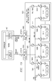
FIG. 14 illustrates a test system according to the present invention. The test system comprises a tester 401, a multiple die probe mechanism 1401, and die 1-N to be tested. The probe mechanism 1401 is similar to the probe mechanism 301 of FIG. 3 in that it has a stimulus channel 302 for probing all common input pads 303 of die 1-N. Probe mechanism 1401 differs from probe mechanism 301 in that it has an encoded response channel for probing all common output pads 1402 of die 1-N. During test, all die 1-N receive a common stimulus input on each common input pad input 303, and all die 1-N receive a common encoded response input on each common output pad 1402. From inspection of the probe mechanism of FIG. 14, it is seen that the test system of the present invention does not suffer from the previously mentioned tester response channel limitation mentioned in regard to the conventional test system of FIG. 3. For example, if the tester 401 has 300 stimulus channels and 300 response channels, and die 1-N have 300 or less input pads and 300 or less output pads, any number of die 1-N may be simultaneously tested using the test system of the present invention. Thus, use of the test system of FIG. 14 reduces the test time of the die on wafer, and therefore reduces the cost to manufacture the die.
FIG. 15 illustrates an alternate view of the test system of FIG. 14. Tester 401 is illustrated as the outer layer, probe mechanism 1401 is illustrated as being inside the tester 401 layer, and wafer 1501 with die 1-N is illustrated as being inside the probe mechanism layer 1401. Each die 1-N are identical and each have inputs 1-M connected to input pads 1502-1504 and 2-state outputs 1-N connected to output pads 1505-1507. The stimulus bus 414 from the tester passes through the probe mechanism to the die input pads 1502-1504. The encoded response bus 411 and response bus 110 from the tester pass through the probe mechanism to the die output pads 1505-1507. Common input pads 1502 of die 1-N are connected together and to one stimulus channel from stimulus bus 414 via the probe mechanism, common input pads 1503 are connected together and to another stimulus channel from stimulus bus 414 via the probe mechanism, and inputs pads 1504 are connected together and to a further stimulus channel from stimulus bus 414 via the probe mechanism. Common output pads 1505 of die 1-N are connected together and to one encoded response channel from encoded response bus 411 via the probe mechanism, common output pads 1506 are connected together and to another encoded response channel from encoded response bus 411 via the probed mechanism, and common output pads 1507 are connected together and to a further encoded response channel from encoded response bus 411 via the probe mechanism.
The pass/fail scan input 611 from the tester passes through the probe mechanism 1401 to the scan input of die 1, through the daisy-chained scan path of die 1-N to be output on the pass/fail scan output 615 to the tester via probe mechanism 1401. The scan input 611 uses one of the stimulus input channels of stimulus bus 414 and the scan output uses one of the response output channels of response output bus 110. While the scan control signals 612, test enable signal 609, and compare strobe signal 613 are not explicitly shown in FIG. 15, they are also connected to die 1-N inputs 1-M via stimulus channels from stimulus input bus 414. While test circuits 606 are shown existing on die 1-N 2-state output pads 1505-1507, it should be clear that test circuits 906 would exist on die 1-N 3-state output pads 1505-1507, and test circuits 1106 would exist on die 1-N I/O pads 1505-1507. If test circuits 1106 were used on die I/O pads 1505-1507, then the encoded response bus 411 would be used to input stimulus data to the I/O pads 1505-1507, via probe mechanism 1401, as described in regard to FIGS. 12A and 12B. Thus is this example, the encoded response bus 411 serves the dual role of; (1) inputting encoded response signals to I/O pads during compare/mask operations, and (2) inputting stimulus data to I/O pads during stimulus input operations.
FIG. 16 illustrates in detail the functional testing of die 1-N (1601-1603) of FIG. 15. Tester 401 inputs stimulus from stimulus bus 414 to common die inputs 1502-1504 via the connections 1609-1611, to allow all die 1-N to receive the same stimulus at their common inputs during test. Connections 1609-1611 are provided by the probe mechanism 1401 of FIGS. 14 and 15. Also, tester 401 inputs stimulus from stimulus bus 414 to the scan input 611 of die 1 via the probe mechanism.
Tester 401 inputs encoded response inputs from encoded response bus 411 to common die outputs and I/Os 1505-1507 via the connections 1606-1608, to allow all die 1-N to receive the same encoded response inputs at their common outputs and I/Os during test. Connections 1606-1608 are provided by the probe mechanism 1401 of FIGS. 14 and 15. Tester 401 inputs a combined fail output signal from die 1-N to response bus 110 via the fail output connection 1605 provided by the probe mechanism. Also, tester 401 inputs the scan output signal 615 from die N to the response bus 110. Connection 1604 illustrates the daisy-chaining of the pass/fail scan output from die 1 to the pass/fail scan input of die 2, and so on to die N. Connection 1604 is provided by the probe mechanism. As seen in FIG. 16, encoded response input 1505 is coupled to 1-N 2-state test circuits 606, encoded response input 1506 is coupled to 1-N 3-state test circuits 906, and encoded response input 1507 is coupled to 1-N I/O test circuits 1106.
During test, tester 401 places the die 1-N in the test mode of the present invention and inputs stimulus patterns to die 1-N inputs via connections 1502-1504 and inputs encoded response patterns to die 1- N test circuits 606, 906, and 1106 via connections 1505-1507. In response to the functional patterns to the inputs and I/Os, die 1-N operates to output data to test circuits 606, output data and control to test circuits 906, and input and output data and control to test circuits 1106. During the test, tester 401 inputs the compare strobe to test circuits 606, 906, and 1106 as previously described to store the compare results between the functional output data and the encoded response input data from the tester. If the test is a production test, the fail output from connection 1605 is ignored during the test for the reasons previously mentioned in regard to FIG. 3. If the test is a diagnostic test, the fail output from connection 1605 is monitored by the tester 401 for the reasons previously mentioned in regard to FIGS. 13A and 13B. At the end of a functional production test or at the stopping of a functional diagnostic test, tester 401 scans out the pass/fail flags in the pass/fail scan memories of die 1-N via the scan input 611 and scan output 615 connections. From the pass/fail scan operation, the tester can determine if a failure occurred in die 1-N and if so identify the location of the failure.
FIG. 17 illustrates in detail the parallel scan testing of die 1-N (1701-1703) of FIG. 15. The difference between die 1-N of FIG. 16 and die 1-N of FIG. 17 is that die 1-N of FIG. 17 have been designed to be tested using a parallel scan design for test approach, whereas die 1-N were not and had to be tested functionally. When die 1-N are placed in the parallel scan test configuration, the data inputs of scan paths 1-N are connected to die inputs 1502-1504 and the data outputs of scan paths 1-N are connected to the inputs 910 of test circuits 606. Tester 401 inputs scan stimulus from bus 414 to die 1-N scan paths 1-N via the common die input connections 1502-1504 and 1609-1611, to allow all die 1-N to receive the same scan stimulus during test. Also, tester 401 inputs stimulus from bus 414 to the scan input 611 of die 1 via the probe mechanism.
Tester 401 inputs encoded scan response from bus 411 to common die output connections 1505-1507 and 1606-1608, to allow all die 1-N to compare against the same response during test. Tester 401 inputs a combined fail output signal from die 1-N to response bus 110 via the fail output connection 1605. Also, tester 401 inputs the scan output signal 615 from die N to the response bus 110. Connection 1604 illustrates the daisy-chaining of the pass/fail scan output from die 1 to the pass/fail scan input of die 2, and so on to die N. As seen in FIG. 17, encoded scan response inputs 1505-1507 are coupled to 1-N 2-state test circuits 606.
During test, tester 401 places the die 1-N in the test mode of the present invention and inputs stimulus patterns to scan paths 1-N of die 1-N via inputs 1502-1504 and inputs encoded response patterns to test circuits 606 of die 1-N via outputs 1505-1507. The scan paths operate, in response to conventional scan path control input from tester 401, to shift in the stimulus patterns from inputs 1502-1504, capture response patterns, and shift out the captured response patterns to test circuits 606. During the test, tester 401 inputs the compare strobe to test circuits 606 as previously described to store the compare results between the captured response data from scan paths 1-N and the encoded response input data from tester 401. If the test is a production test, the fail output from connection 1605 is ignored during the test for the reasons previously mentioned in regard to FIG. 3. If the test is a diagnostic test, the fail output from connection 1605 is monitored by the tester 401 for the reasons previously mentioned in regard to FIGS. 13A and 13B. At the end of a parallel scan production test or at the stopping of a parallel scan diagnostic test, tester 401 scans out the pass/fail flags in the pass/fail scan memories of die 1-N via the scan input 611 and scan output 615 connections. From the pass/fail scan operation, the tester can determine if a failure occurred in die 1-N and if so identify the location of the failure.
It is becoming increasingly popular to design systems on ICs using pre-existing intellectual property core sub-circuits. Core sub-circuits provide embeddable functions such as DSP, CPU, and RAM. FIG. 18A illustrates an IC comprising embedded cores 1-3. The cores are connected together via functional connections 1814 and 1815 to form a system on the IC. The following describes how such systems on ICs can be tested using the present invention.
To test the embedded cores 1-3 of IC 1802, test connections 1810 and connection circuits 1808 and 1809 are added to allow input pads 1803 to be selectively connected to the inputs of cores 1-3. Also test connections 1811, 1812 and 1818 are added to allow the outputs of cores 1-3 to be connected to test circuits 1813, which are coupled to output pads 1802. As seen in FIG. 18B, test circuit 1813 is similar to test circuit 606 with the exception that it contains a multiplexer 1816 for receiving core 1-3 outputs 1811, 1812, and 1818 and a core select input 1817 for selecting which of the core 1-3 outputs 1811, 1812, or 1818 will be selected for input to buffer 607 and compare circuit 608.
During the testing of core 1, the IC of FIG. 18A is configured such that the inputs to core 1 are coupled to input pads 1803 and the outputs from core 1 are coupled to test circuits 1813 via connections 1811. Also test circuit 1813 is configured by the core select signals 1816 to connect the core 1 outputs to compare circuits 608. After the IC has been configured, core 1 is rendered testable using the present invention by inputting stimulus to core 1 via pads 1803 and inputting encoded response to test circuit 1813 via pads 1802 to compare against the outputs from core 1. The testing of core 1 is as previously described in FIGS. 6A and 6B.
During the testing of core 2, the IC of FIG. 18A is configured such that the inputs to core 2 are coupled to input pads 1803, via connection 1810 and connection circuit 1808, and the outputs from core 2 are coupled to test circuits 1813 via connections 1812. Also test circuit 1813 is configured by the core select signals 1816 to connect the core 2 outputs to compare circuits 608. After the IC has been configured, core 2 is rendered testable using the present invention by inputting stimulus to core 2 via pads 1803 and inputting encoded response to test circuit 1813 via pads 1802 to compare against the outputs from core 2. The testing of core 2 is as previously described in FIGS. 6A and 6B.
During the testing of core 3, the IC of FIG. 18A is configured such that the inputs to core 3 are coupled to input pads 1803, via connection 1810 and connection circuit 1809, and the outputs from core 3 are coupled to test circuits 1813 via connections 1818. Also test circuit 1813 is configured by the core select signals 1816 to connect the core 3 outputs to compare circuits 608. After the IC has been configured, core 3 is rendered testable using the present invention by inputting stimulus to core 3 via pads 1803 and inputting encoded response to test circuit 1813 via pads 1802 to compare against the outputs from core 3. The testing of core 3 is as previously described in FIGS. 6A and 6B.
The individual core 1-3 tests described above could be performed simultaneously on multiple ICs of FIG. 18A as described in regard FIG. 15, which would lower the cost to manufacture the ICs of FIG. 18A.
FIG. 19 illustrates a wafer 1901 which has been processed to include built-in connections for accessing common die input (S1) and common die output (R1) pads. The wafer comprises; (1) die 1-N each with input (S1) pads and output (R1) pads, (2) stimulus input grid lines 1904 connected to common die input pads, (3) encoded response input grid lines 1905 connected to common die output pads, (4) pad fuses 1906 connected in series between grid lines 1905 and pad connection lines 1907, 1908, 1909, and 1910, (5) tester probe contacts 1903 for connecting to stimulus grid lines 1904, and (6) tester probe contacts 1902 for connecting to encoded response grid lines 1905.
Tester 401 probes grid line contacts 1903, 1902 using a simplified external probe mechanism to input stimulus to the commonly connected die input pads and to input encoded response to the commonly connected die output pads. Testing occurs on the die as previously described. The difference between the test systems of FIG. 19 and FIG. 14 is that in FIG. 19 most of the common pad connections are provided on the wafer 1901, whereas in FIG. 14 most of the common pad connections are provided by the external probe mechanism 1401.
The fuses 1906 are included between grid lines 1905 and common pad connections 1907-1910 to provide for the case where a faulty die output cannot be disabled by the test enable signal 609. For example, if the tester 401 sets the test enable signal 609 high to enable testing using the present invention, and the output pad of die 3 remains enabled outputting a logic level, the fuse 1906 between gird line 1905 and the enabled output pad of die 3 will blow whenever the tester inputs an oppose logic level on grid line 1905. Without the fuse, the logic level maintained on the output pad of die 3 could prevent testing of the other die on wafer due to logic state contention on grid line 1905. Alternatively, a resistive element could be substituted for each fuse 1906 to provide current limiting between a faulty die output pad and tester to enable testing of the other die. After testing and prior to the die singulation step, the pad connecting grid lines, probe contacts, and fuses/resistive elements can be polished off the wafer 1901.
It should be noted that if wafers were processed to include the embedded pad connection scheme shown on wafer 1901 of FIG. 19, tester 401 could probe multiple ones of the wafers 1901 at common probe contacts 1903 and 1902 to enable simultaneous testing of multiple wafers 1901. Being able to test multiple wafers simultaneously using one tester 401 would bring about further reductions in test time and cost of manufacturing die. For clarity, an example illustration of the above described multiple wafer test approach is depicted in FIG. 19A. In the example, tester 401 makes contact to probe contacts 1903 and 1902 of wafers 1901 via the previously described multiple wafer probe mechanism 1401 of FIG. 14. The only difference between FIGS. 14 and 19A is that in FIG. 14 multiple die are tested whereas in FIG. 19A multiple wafers are tested.
While the present invention has been described thus far a being used to simultaneously test multiple die on wafer and, as mentioned in regard to FIG. 19, even multiple wafers, it can also be used to simultaneously test multiple packaged ICs as well. FIG. 20 illustrates a test system according to the present invention for simultaneously testing multiple packaged ICs 1-N. The test system comprises a tester 401, a multiple IC probe mechanism 2001, and identical packaged ICs 1-N to be tested. In this example, ICs 1-N each comprise a die 601, a package 2002 for holding die 601, bond wires 2003 for connecting the output pads 603 of die 601 to package output leads 2004, and bond wires 2005 for connecting input pads 602 of die 601 to package input leads 2006.
The process of testing ICs 1-N in FIG. 20 is the same as that described in the testing of die 1-N in FIG. 14. The only difference between the two tests is that the packaged die 601 of FIG. 20 are connected to the IC probe mechanism 2001 via bond wires 2005 and 2003 and input and output package leads 2006 and 2004. It is assumed in FIG. 20 that each IC 1-N has package leads available for the test enable 609, scan control 612, scan input 611, scan output 615, compare strobe 613, and fail output 1302 signals. However, if not all the signals are available on package leads, they may be provided by sharing functional package leads or by generating the signals internal to the die using test interfaces such as the EEE standard 1149.1 test access port interface.

Claims (5)

What is claimed is:
1. An integrated circuit comprising:
A. input pads;
B. output pads;
C. first core circuitry having an input coupled to an input pad and having an output;
D. second core circuitry having an input coupled to the output of the first core circuitry and having an output coupled to an output pad;
E. test connection circuitry having an input coupled with the input pad and having an output coupled with the input of the second core circuitry; and
F. output circuitry including:
i. a tri-state buffer having a core input, a data output coupled to an output pad, and a tristate enable input;
ii. comparator circuitry having a core input coupled to the core input of the tri-state buffer, a response input coupled to the output pad, and an enable input lead coupled to the tristate enable input of the tri-state buffer; and
iii. multiplex circuitry having a first input coupled to the output of the first core circuitry, a second input coupled to the output of the second core circuitry, a core select input, and a selected core output coupled to the core input of the tri-state buffer circuitry.
2. The integrated circuit of claim 1 in which the comparator circuitry includes a serial scan input lead, a serial scan output lead, a serial scan control input lead and a compare strobe input lead.
3. The integrated circuit of claim 1 in which the comparator circuitry includes compare gates, a pass/fail latch, and a scan cell, the compare gates being coupled to the core input lead and the response lead, the pass/fail latch being coupled to the output of the compare gates to store the result of a compare, and the scan cell being coupled to the output of the pass/fail latch and having an scan input lead, a scan output lead and a scan control lead.
4. The integrated circuit of claim 3 in which the pass/fail latch includes an AND gate coupled to the compare gates and a flip-flop coupled to the AND gate.
5. The integrated circuit of claim 3 in which the scan cell includes a multiplexer coupled to the output of the flip-flop, the scan input lead and the scan control lead, and a flip-flop coupled to the output of the multiplexer, the scan output lead and the scan control lead.
US14/807,214 2000-06-30 2015-07-23 Semiconductor test system and method Expired - Fee Related US9222977B2 (en)

Priority Applications (2)

Application Number Priority Date Filing Date Title
US14/807,214 US9222977B2 (en) 2000-06-30 2015-07-23 Semiconductor test system and method
US14/944,903 US9417283B2 (en) 2000-06-30 2015-11-18 Semiconductor test system and method

Applications Claiming Priority (13)

Application Number Priority Date Filing Date Title
US21524700P 2000-06-30 2000-06-30
US09/896,467 US6717429B2 (en) 2000-06-30 2001-06-29 IC having comparator inputs connected to core circuitry and output pad
US10/806,546 US7183789B2 (en) 2000-06-30 2004-03-23 Comparing on die response and expected response applied to outputs
US11/623,370 US8020057B2 (en) 2000-06-30 2007-01-16 Comparator circuitry connected to input and output of tristate buffer
US13/198,336 US8219862B2 (en) 2000-06-30 2011-08-04 Pass/fail scan memory with AND, OR and trinary gates
US13/523,470 US8453024B2 (en) 2000-06-30 2012-06-14 I/O and comparator circuitry with compare gate and mask circuitry
US13/870,238 US8572446B2 (en) 2000-06-30 2013-04-25 Output circuitry with tri-state buffer and comparator circuitry
US13/909,384 US8607109B2 (en) 2000-06-30 2013-06-04 Test circuitry including core output, expected response, and mask circuitry
US14/074,402 US8700963B2 (en) 2000-06-30 2013-11-07 Semiconductor test system and method
US14/191,964 US8880967B2 (en) 2000-06-30 2014-02-27 Semiconductor test system and method
US14/504,649 US9003249B2 (en) 2000-06-30 2014-10-02 IC test circuitry with tri-state buffer, comparator, and scan cell
US14/637,098 US9121906B2 (en) 2000-06-30 2015-03-03 Semiconductor test system and method
US14/807,214 US9222977B2 (en) 2000-06-30 2015-07-23 Semiconductor test system and method

Related Parent Applications (1)

Application Number Title Priority Date Filing Date
US14/637,098 Division US9121906B2 (en) 2000-06-30 2015-03-03 Semiconductor test system and method

Related Child Applications (1)

Application Number Title Priority Date Filing Date
US14/944,903 Division US9417283B2 (en) 2000-06-30 2015-11-18 Semiconductor test system and method

Publications (2)

Publication Number Publication Date
US20150323601A1 US20150323601A1 (en) 2015-11-12
US9222977B2 true US9222977B2 (en) 2015-12-29

Family

ID=26909860

Family Applications (12)

Application Number Title Priority Date Filing Date
US09/896,467 Expired - Lifetime US6717429B2 (en) 2000-06-30 2001-06-29 IC having comparator inputs connected to core circuitry and output pad
US10/806,546 Expired - Lifetime US7183789B2 (en) 2000-06-30 2004-03-23 Comparing on die response and expected response applied to outputs
US11/623,370 Expired - Fee Related US8020057B2 (en) 2000-06-30 2007-01-16 Comparator circuitry connected to input and output of tristate buffer
US13/198,336 Expired - Fee Related US8219862B2 (en) 2000-06-30 2011-08-04 Pass/fail scan memory with AND, OR and trinary gates
US13/523,470 Expired - Fee Related US8453024B2 (en) 2000-06-30 2012-06-14 I/O and comparator circuitry with compare gate and mask circuitry
US13/909,384 Expired - Fee Related US8607109B2 (en) 2000-06-30 2013-06-04 Test circuitry including core output, expected response, and mask circuitry
US14/074,402 Expired - Fee Related US8700963B2 (en) 2000-06-30 2013-11-07 Semiconductor test system and method
US14/191,964 Expired - Fee Related US8880967B2 (en) 2000-06-30 2014-02-27 Semiconductor test system and method
US14/504,649 Expired - Fee Related US9003249B2 (en) 2000-06-30 2014-10-02 IC test circuitry with tri-state buffer, comparator, and scan cell
US14/637,098 Expired - Fee Related US9121906B2 (en) 2000-06-30 2015-03-03 Semiconductor test system and method
US14/807,214 Expired - Fee Related US9222977B2 (en) 2000-06-30 2015-07-23 Semiconductor test system and method
US14/944,903 Expired - Fee Related US9417283B2 (en) 2000-06-30 2015-11-18 Semiconductor test system and method

Family Applications Before (10)

Application Number Title Priority Date Filing Date
US09/896,467 Expired - Lifetime US6717429B2 (en) 2000-06-30 2001-06-29 IC having comparator inputs connected to core circuitry and output pad
US10/806,546 Expired - Lifetime US7183789B2 (en) 2000-06-30 2004-03-23 Comparing on die response and expected response applied to outputs
US11/623,370 Expired - Fee Related US8020057B2 (en) 2000-06-30 2007-01-16 Comparator circuitry connected to input and output of tristate buffer
US13/198,336 Expired - Fee Related US8219862B2 (en) 2000-06-30 2011-08-04 Pass/fail scan memory with AND, OR and trinary gates
US13/523,470 Expired - Fee Related US8453024B2 (en) 2000-06-30 2012-06-14 I/O and comparator circuitry with compare gate and mask circuitry
US13/909,384 Expired - Fee Related US8607109B2 (en) 2000-06-30 2013-06-04 Test circuitry including core output, expected response, and mask circuitry
US14/074,402 Expired - Fee Related US8700963B2 (en) 2000-06-30 2013-11-07 Semiconductor test system and method
US14/191,964 Expired - Fee Related US8880967B2 (en) 2000-06-30 2014-02-27 Semiconductor test system and method
US14/504,649 Expired - Fee Related US9003249B2 (en) 2000-06-30 2014-10-02 IC test circuitry with tri-state buffer, comparator, and scan cell
US14/637,098 Expired - Fee Related US9121906B2 (en) 2000-06-30 2015-03-03 Semiconductor test system and method

Family Applications After (1)

Application Number Title Priority Date Filing Date
US14/944,903 Expired - Fee Related US9417283B2 (en) 2000-06-30 2015-11-18 Semiconductor test system and method

Country Status (1)

Country Link
US (12) US6717429B2 (en)

Families Citing this family (38)

* Cited by examiner, † Cited by third party
Publication number Priority date Publication date Assignee Title
US6551844B1 (en) * 1997-01-15 2003-04-22 Formfactor, Inc. Test assembly including a test die for testing a semiconductor product die
US6717429B2 (en) * 2000-06-30 2004-04-06 Texas Instruments Incorporated IC having comparator inputs connected to core circuitry and output pad
US8572446B2 (en) * 2000-06-30 2013-10-29 Texas Instruments Incorporated Output circuitry with tri-state buffer and comparator circuitry
TW498476B (en) * 2001-08-30 2002-08-11 Macronix Int Co Ltd Synchronization test method and circuit for the segment of memory
US6894308B2 (en) * 2001-11-28 2005-05-17 Texas Instruments Incorporated IC with comparator receiving expected and mask data from pads
US7412639B2 (en) * 2002-05-24 2008-08-12 Verigy (Singapore) Pte. Ltd. System and method for testing circuitry on a wafer
US7119567B2 (en) * 2002-09-12 2006-10-10 Infineon Technologies North America Corp. System and method for testing one or more dies on a semiconductor wafer
US7231552B2 (en) * 2002-10-24 2007-06-12 Intel Corporation Method and apparatus for independent control of devices under test connected in parallel
US6941232B2 (en) * 2003-01-28 2005-09-06 Texas Instruments Incorporated Method and apparatus for performing multi-site integrated circuit device testing
US6788095B1 (en) * 2003-01-31 2004-09-07 Xilinx, Inc. Method for gross input leakage functional test at wafer sort
US20050005436A1 (en) * 2003-07-09 2005-01-13 Jung-Chien Chang Method for preparing thin integrated circuits with multiple circuit layers
DE10335809B4 (en) * 2003-08-05 2010-07-01 Infineon Technologies Ag Integrated circuit with an electronic circuit under test and test system arrangement for testing the integrated circuit
KR100576824B1 (en) * 2003-11-27 2006-05-10 삼성전자주식회사 Semiconductor memory integrated circuit and layout method of the same
US20050147048A1 (en) * 2004-01-07 2005-07-07 Haehn Steven L. Low cost test option using redundant logic
US7356745B2 (en) 2004-02-06 2008-04-08 Texas Instruments Incorporated IC with parallel scan paths and compare circuitry
US7471098B2 (en) * 2004-10-28 2008-12-30 Seagate Technology Llc Testing device and method for an integrated circuit
US20060242508A1 (en) * 2005-04-26 2006-10-26 Texas Instruments Incorporation Simultaneous scan testing for identical modules
US20070051949A1 (en) * 2005-09-06 2007-03-08 Peter Schneider Method and arrangment for testing a stacked die semiconductor device
US7580807B2 (en) * 2006-06-15 2009-08-25 Texas Instruments Incorporated Test protocol manager for massive multi-site test
US8093919B2 (en) * 2006-11-10 2012-01-10 Nec Corporation Test circuit, method, and semiconductor device
US8115507B2 (en) * 2006-11-10 2012-02-14 Nec Corporation Circuit and method for parallel testing and semiconductor device
US8829940B2 (en) * 2008-09-26 2014-09-09 Nxp, B.V. Method for testing a partially assembled multi-die device, integrated circuit die and multi-die device
US8639855B2 (en) * 2008-10-20 2014-01-28 International Business Machines Corporation Information collection and storage for single core chips to 'N core chips
JP2011149775A (en) * 2010-01-20 2011-08-04 Renesas Electronics Corp Semiconductor integrated circuit and core test circuit
KR101294852B1 (en) * 2010-10-13 2013-08-08 엘지디스플레이 주식회사 Micro Controller, Driving Method thereof and Display Device using the same
TW201225529A (en) * 2010-12-03 2012-06-16 Fortune Semiconductor Corp Test mode controller and electronic apparatus with self-testing thereof
US9064074B2 (en) * 2011-11-14 2015-06-23 International Business Machines Corporation Retrieving odd net topology in hierarchical circuit designs
US9037931B2 (en) * 2011-12-21 2015-05-19 Advanced Micro Devices, Inc. Methods and systems for logic device defect tolerant redundancy
US9196329B1 (en) * 2012-11-29 2015-11-24 Marvell Israel (M.I.S.L) Ltd. Combinatorial flip flop with off-path scan multiplexer
US9032256B2 (en) * 2013-01-11 2015-05-12 International Business Machines Corporation Multi-core processor comparison encoding
KR102317023B1 (en) 2014-08-14 2021-10-26 삼성전자주식회사 semiconductor device, method and apparatus for manufacturing the same
US9829536B2 (en) * 2016-02-03 2017-11-28 Nvidia Corporation Performing on-chip partial good die identification
JP6782134B2 (en) * 2016-09-26 2020-11-11 ラピスセミコンダクタ株式会社 Scan circuits, collective scan circuits, semiconductor devices, and semiconductor device inspection methods
KR102615775B1 (en) * 2017-01-31 2023-12-20 에스케이하이닉스 주식회사 Semiconductor device
CN107422244A (en) * 2017-05-18 2017-12-01 苏州大学 The chaos source current method of fault detection
US10509074B2 (en) * 2018-02-22 2019-12-17 Taiwan Semiconductor Manufacturing Company, Ltd. Electrical testing apparatus for spintronics devices
US10845407B2 (en) * 2018-06-25 2020-11-24 Intel Corporation Scalable infield scan coverage for multi-chip module for functional safety mission application
TW202303161A (en) * 2021-06-25 2023-01-16 美商Ic分析有限責任公司 Apparatus and method for probing multiple test circuits in wafer scribe lines

Citations (12)

* Cited by examiner, † Cited by third party
Publication number Priority date Publication date Assignee Title
US6009026A (en) * 1997-07-28 1999-12-28 International Business Machines Corporation Compressed input/output test mode
US6169418B1 (en) * 1998-06-24 2001-01-02 S3 Incorporated Efficient routing from multiple sources to embedded DRAM and other large circuit blocks
US6215324B1 (en) * 1999-01-07 2001-04-10 Nippon Scientific Co., Ltd. Dynamic burn-in test equipment
US20030046622A1 (en) * 1998-06-19 2003-03-06 Whetsel Lee D. Integrated circuits carrying intellectual property cores and test ports
US6591211B1 (en) * 1999-08-27 2003-07-08 Intel Corporation Testing unit and self-evaluating device
US6618827B1 (en) * 2000-04-13 2003-09-09 Hewlett-Packard Development Company, L.P. System and method for parallel testing of IEEE 1149.1 compliant integrated circuits
US6694463B2 (en) * 2001-01-16 2004-02-17 Atmel Corporation Input/output continuity test mode circuit
US6694464B1 (en) * 1997-05-30 2004-02-17 Quickturn Design Systems, Inc. Method and apparatus for dynamically testing electrical interconnect
US6717429B2 (en) * 2000-06-30 2004-04-06 Texas Instruments Incorporated IC having comparator inputs connected to core circuitry and output pad
US20040199839A1 (en) * 1988-09-07 2004-10-07 Whetsel Lee D. Changing scan cell output signal states with a clock signal
US6894308B2 (en) * 2001-11-28 2005-05-17 Texas Instruments Incorporated IC with comparator receiving expected and mask data from pads
US7356745B2 (en) * 2004-02-06 2008-04-08 Texas Instruments Incorporated IC with parallel scan paths and compare circuitry

Family Cites Families (10)

* Cited by examiner, † Cited by third party
Publication number Priority date Publication date Assignee Title
US5032789A (en) * 1989-06-19 1991-07-16 Hewlett-Packard Company Modular/concurrent board tester
US5101150A (en) * 1991-02-22 1992-03-31 Genrad, Inc. Automatic circuit tester with separate instrument and scanner buses
US5406197A (en) * 1992-07-31 1995-04-11 International Business Machines Corporation Apparatus for controlling test inputs of circuits on an electronic module
JP3135378B2 (en) * 1992-08-10 2001-02-13 ローム株式会社 Semiconductor test equipment
US5912563A (en) * 1997-05-22 1999-06-15 Sun Microsystems, Inc. Trinary signal apparatus and method
KR100294021B1 (en) * 1998-09-08 2001-07-12 윤종용 Memory module test device
US6292415B1 (en) * 1999-09-28 2001-09-18 Aehr Test Systems, Inc. Enhancements in testing devices on burn-in boards
US6424583B1 (en) * 2000-11-30 2002-07-23 Taiwan Semiconductor Manufacturing Co., Ltd System and measuring access time of embedded memories
US6762614B2 (en) * 2002-04-18 2004-07-13 Agilent Technologies, Inc. Systems and methods for facilitating driver strength testing of integrated circuits
US20050204217A1 (en) * 2004-02-06 2005-09-15 Whetsel Lee D. Identical core testing using dedicated compare and mask circuitry

Patent Citations (23)

* Cited by examiner, † Cited by third party
Publication number Priority date Publication date Assignee Title
US20040199839A1 (en) * 1988-09-07 2004-10-07 Whetsel Lee D. Changing scan cell output signal states with a clock signal
US6694464B1 (en) * 1997-05-30 2004-02-17 Quickturn Design Systems, Inc. Method and apparatus for dynamically testing electrical interconnect
US6009026A (en) * 1997-07-28 1999-12-28 International Business Machines Corporation Compressed input/output test mode
US20030046622A1 (en) * 1998-06-19 2003-03-06 Whetsel Lee D. Integrated circuits carrying intellectual property cores and test ports
US6560734B1 (en) * 1998-06-19 2003-05-06 Texas Instruments Incorporated IC with addressable test port
US6169418B1 (en) * 1998-06-24 2001-01-02 S3 Incorporated Efficient routing from multiple sources to embedded DRAM and other large circuit blocks
US6215324B1 (en) * 1999-01-07 2001-04-10 Nippon Scientific Co., Ltd. Dynamic burn-in test equipment
US6591211B1 (en) * 1999-08-27 2003-07-08 Intel Corporation Testing unit and self-evaluating device
US6618827B1 (en) * 2000-04-13 2003-09-09 Hewlett-Packard Development Company, L.P. System and method for parallel testing of IEEE 1149.1 compliant integrated circuits
US6717429B2 (en) * 2000-06-30 2004-04-06 Texas Instruments Incorporated IC having comparator inputs connected to core circuitry and output pad
US20140181609A1 (en) * 2000-06-30 2014-06-26 Texas Instruments Incorporated Semiconductor test system and method
US7183789B2 (en) * 2000-06-30 2007-02-27 Texas Instruments Incorporated Comparing on die response and expected response applied to outputs
US8453024B2 (en) * 2000-06-30 2013-05-28 Texas Instruments Incorporated I/O and comparator circuitry with compare gate and mask circuitry
US8219862B2 (en) * 2000-06-30 2012-07-10 Texas Instruments Incorporated Pass/fail scan memory with AND, OR and trinary gates
US8020057B2 (en) * 2000-06-30 2011-09-13 Texas Instruments Incorporated Comparator circuitry connected to input and output of tristate buffer
US6694463B2 (en) * 2001-01-16 2004-02-17 Atmel Corporation Input/output continuity test mode circuit
US7842949B2 (en) * 2001-11-28 2010-11-30 Texas Instruments Incorporated IC with comparator receiving expected and mask data from pads
US7655946B2 (en) * 2001-11-28 2010-02-02 Texas Instruments Incorporated IC with comparator receiving expected and mask data from pads
US7491970B2 (en) * 2001-11-28 2009-02-17 Texas Instruments Incorporated IC with comparator receiving expected and mask data from pads
US8299464B2 (en) * 2001-11-28 2012-10-30 Texas Instruments Incorporated Comparator receiving expected and mask data from circuit pads
US20070114529A1 (en) * 2001-11-28 2007-05-24 Texas Instruments Incorporated Scan testing system, method and apparatus
US6894308B2 (en) * 2001-11-28 2005-05-17 Texas Instruments Incorporated IC with comparator receiving expected and mask data from pads
US7356745B2 (en) * 2004-02-06 2008-04-08 Texas Instruments Incorporated IC with parallel scan paths and compare circuitry

Non-Patent Citations (1)

* Cited by examiner, † Cited by third party
Title
Whetsel, L., "Addressable test ports an approach to testing embedded cores," Test Conference, 1999. Proceedings. International, vol., no., pp. 1055-1064, 1999. *

Also Published As

Publication number Publication date
US8880967B2 (en) 2014-11-04
US9003249B2 (en) 2015-04-07
US8020057B2 (en) 2011-09-13
US8700963B2 (en) 2014-04-15
US20140181609A1 (en) 2014-06-26
US9417283B2 (en) 2016-08-16
US20150019928A1 (en) 2015-01-15
US20140068363A1 (en) 2014-03-06
US20150177325A1 (en) 2015-06-25
US20020021140A1 (en) 2002-02-21
US20150323601A1 (en) 2015-11-12
US20070136630A1 (en) 2007-06-14
US20130275825A1 (en) 2013-10-17
US20040181721A1 (en) 2004-09-16
US6717429B2 (en) 2004-04-06
US20110296263A1 (en) 2011-12-01
US20120260140A1 (en) 2012-10-11
US8607109B2 (en) 2013-12-10
US7183789B2 (en) 2007-02-27
US9121906B2 (en) 2015-09-01
US20160069949A1 (en) 2016-03-10
US8453024B2 (en) 2013-05-28
US8219862B2 (en) 2012-07-10

Similar Documents

Publication Publication Date Title
US9417283B2 (en) Semiconductor test system and method
US10120025B2 (en) Functional core circuitry with serial scan test expected, mask circuitry
US8572446B2 (en) Output circuitry with tri-state buffer and comparator circuitry

Legal Events

Date Code Title Description
STCF Information on status: patent grant

Free format text: PATENTED CASE

MAFP Maintenance fee payment

Free format text: PAYMENT OF MAINTENANCE FEE, 4TH YEAR, LARGE ENTITY (ORIGINAL EVENT CODE: M1551); ENTITY STATUS OF PATENT OWNER: LARGE ENTITY

Year of fee payment: 4

FEPP Fee payment procedure

Free format text: MAINTENANCE FEE REMINDER MAILED (ORIGINAL EVENT CODE: REM.); ENTITY STATUS OF PATENT OWNER: LARGE ENTITY

LAPS Lapse for failure to pay maintenance fees

Free format text: PATENT EXPIRED FOR FAILURE TO PAY MAINTENANCE FEES (ORIGINAL EVENT CODE: EXP.); ENTITY STATUS OF PATENT OWNER: LARGE ENTITY

STCH Information on status: patent discontinuation

Free format text: PATENT EXPIRED DUE TO NONPAYMENT OF MAINTENANCE FEES UNDER 37 CFR 1.362

FP Lapsed due to failure to pay maintenance fee

Effective date: 20231229