US9203254B2 - Power management circuit for a portable electronic device including USB functionality and method for doing the same - Google Patents
Power management circuit for a portable electronic device including USB functionality and method for doing the same Download PDFInfo
- Publication number
- US9203254B2 US9203254B2 US13/819,168 US201113819168A US9203254B2 US 9203254 B2 US9203254 B2 US 9203254B2 US 201113819168 A US201113819168 A US 201113819168A US 9203254 B2 US9203254 B2 US 9203254B2
- Authority
- US
- United States
- Prior art keywords
- interface
- buck
- boost
- voltage
- circuit
- Prior art date
- Legal status (The legal status is an assumption and is not a legal conclusion. Google has not performed a legal analysis and makes no representation as to the accuracy of the status listed.)
- Active, expires
Links
Images


Classifications
-
- H02J7/0052—
-
- G—PHYSICS
- G06—COMPUTING; CALCULATING OR COUNTING
- G06F—ELECTRIC DIGITAL DATA PROCESSING
- G06F1/00—Details not covered by groups G06F3/00 - G06F13/00 and G06F21/00
- G06F1/26—Power supply means, e.g. regulation thereof
- G06F1/263—Arrangements for using multiple switchable power supplies, e.g. battery and AC
-
- H—ELECTRICITY
- H02—GENERATION; CONVERSION OR DISTRIBUTION OF ELECTRIC POWER
- H02J—CIRCUIT ARRANGEMENTS OR SYSTEMS FOR SUPPLYING OR DISTRIBUTING ELECTRIC POWER; SYSTEMS FOR STORING ELECTRIC ENERGY
- H02J1/00—Circuit arrangements for dc mains or dc distribution networks
- H02J1/10—Parallel operation of dc sources
- H02J1/102—Parallel operation of dc sources being switching converters
-
- H—ELECTRICITY
- H02—GENERATION; CONVERSION OR DISTRIBUTION OF ELECTRIC POWER
- H02J—CIRCUIT ARRANGEMENTS OR SYSTEMS FOR SUPPLYING OR DISTRIBUTING ELECTRIC POWER; SYSTEMS FOR STORING ELECTRIC ENERGY
- H02J7/00—Circuit arrangements for charging or depolarising batteries or for supplying loads from batteries
-
- H02J7/0055—
-
- H02J7/0065—
-
- H—ELECTRICITY
- H02—GENERATION; CONVERSION OR DISTRIBUTION OF ELECTRIC POWER
- H02J—CIRCUIT ARRANGEMENTS OR SYSTEMS FOR SUPPLYING OR DISTRIBUTING ELECTRIC POWER; SYSTEMS FOR STORING ELECTRIC ENERGY
- H02J7/00—Circuit arrangements for charging or depolarising batteries or for supplying loads from batteries
- H02J7/0068—Battery or charger load switching, e.g. concurrent charging and load supply
-
- H02J2007/0062—
-
- H—ELECTRICITY
- H02—GENERATION; CONVERSION OR DISTRIBUTION OF ELECTRIC POWER
- H02J—CIRCUIT ARRANGEMENTS OR SYSTEMS FOR SUPPLYING OR DISTRIBUTING ELECTRIC POWER; SYSTEMS FOR STORING ELECTRIC ENERGY
- H02J2207/00—Indexing scheme relating to details of circuit arrangements for charging or depolarising batteries or for supplying loads from batteries
- H02J2207/20—Charging or discharging characterised by the power electronics converter
-
- H—ELECTRICITY
- H02—GENERATION; CONVERSION OR DISTRIBUTION OF ELECTRIC POWER
- H02J—CIRCUIT ARRANGEMENTS OR SYSTEMS FOR SUPPLYING OR DISTRIBUTING ELECTRIC POWER; SYSTEMS FOR STORING ELECTRIC ENERGY
- H02J2207/00—Indexing scheme relating to details of circuit arrangements for charging or depolarising batteries or for supplying loads from batteries
- H02J2207/40—Indexing scheme relating to details of circuit arrangements for charging or depolarising batteries or for supplying loads from batteries adapted for charging from various sources, e.g. AC, DC or multivoltage
Definitions
- the invention relates to the field of electronic circuits and more particular to an Energy and Power management circuit for a telecommunication product, such as a mobile telephone offering different interfaces (USB, OTG, SIM . . . )
- a recent mobile telephone typically includes two separate battery charging circuits: the conventional AC/DC battery charging circuit and, recently, a DC/DC charging circuit for allowing the charging of the battery through the well-known Universal Serial Bus (USB) interface.
- USB Universal Serial Bus
- FIG. 1 illustrates the general architecture of a two-ways charging circuit for charging a battery 100 of a conventional mobile telephone.
- a first USB charger circuit is based on a buck converter 110 including two switches SA and SB referenced 111 and 112 ) in addition to a first coil 113 in series with a resistance 114 .
- a second charging circuit is connected to the mains and comprises second buck converter 120 including two switches SC and SC (resp. 121 and 122 ) in additional to a second coil 123 in series with a resistance 124 .
- Coils 113 and 123 are electronic components which are dedicated to remain outside of the integrated chip and, for the sake of clarity, the different “balls” of the integrated semiconductor have been represented in the figures under the reference 191 - 199 .
- FIG. 1 shows that, when the electronic mobile is plugged on the alternative mains, then it is the buck converter 120 of the figure which achieves recharging of battery 100 as known by the skilled man.
- the buck converter 110 is being active when the USB interface is plugged so as to receiver current which can be, after conversion by the buck converter 120 , used for charging battery 100 .
- buck converter 120 is used to serve as a pump charge or a boost converter so as to perform Step Up voltage conversion so as to generate the so-called On The Go (OTG) voltage required by the peripheral connected to the USB interface.
- OTG On The Go
- a modern mobile phone requires two distinctive buck converter, one being particularly a buck/boost converter for providing two battery charging circuits through mains/USB and also for achieving OTG compatibility.
- a Power Management circuit for a portable electronic device comprising an internal battery to be charged either through a first interface (USB) or through the conventional AC-DC conversion circuit.
- the circuit comprises a first buck/boost converter having a Switched Mode Power Supply (SMPS) mode which can be controlled either in a buck or a boost mode and also associated with a first coil so as to serve as a first charging circuit (USB) for the battery.
- SMPS Switched Mode Power Supply
- the circuit further includes a second buck/boost converter which can also be controlled either in a buck or a boost mode and serving to charge the battery through the mains, the second converter being also associated with a second external coil for the purpose of carrying out a second charging circuit for the battery.
- a second buck/boost converter which can also be controlled either in a buck or a boost mode and serving to charge the battery through the mains, the second converter being also associated with a second external coil for the purpose of carrying out a second charging circuit for the battery.
- the circuit further comprising by-pass circuits, under control of a control circuit, for the purpose of performing a by-pass of either the voltage of the battery or the voltage generated by one of the two buck/boost controllers when in boost mode so as to generate a voltage which can be used as a further interface (SIM/MMC).
- SIM/MMC further interface
- the first interface is a Universal Bus Interface (USB).
- USB Universal Bus Interface
- the second interface is a SIM interface.
- it can be a MMC interface for receiving a memory card.
- the Power Management circuit is used in a mobile telephone.
- the invention also achieves a method of power management for a portable electronic device comprising an internal battery to be charged either through a USB interface or a AC/DC interface.
- the method involves the steps of:
- the method further performing the steps of:
- FIG. 1 illustrates a conventional architecture of a conventional energy and power management circuit for a mobile telephone.
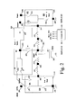
- FIG. 2 illustrates the circuit of one embodiment of an Energy and Power Management circuit in accordance with the invention.
- FIGS. 3 and 4 respectively illustrate the logic of the control circuit 250 for the purpose of generating the SIM or MMC voltage at the ball VIF.
- the invention will be particularly described in reference with a Universal Serial Bus interface which is today widely used for performing the charging of the battery, alternatively to the conventional AC/DC conversion.
- the embodiment illustrated in FIG. 2 thus includes two battery charging circuits based on two buck converters, 210 and 220 respectively, so as to achieve fast charging (typically 1500 mA/h) of a high capacity battery 200 .
- the circuit comprises a first buck/boost converter 210 associated with a first external coil 213 connected in series with a resistance 214 for the purpose of embodying a first battery charging circuit through an USB interface.
- the buck converter 210 is also arranged to be a boost converter so as to performing a UP conversion of the voltage of the battery in order to produce a higher voltage (5V) at the USB interface so as to supply current to a peripheral connected to said USB interface;
- the Energy and Power management circuit further includes a second buck converter 220 which is associated with a second external coil 223 in series with a resistance 224 so as embody an alternate charging circuit connected to the conventional AC/DC circuit connected to the mains.
- the second buck converter 220 is arranged, in the embodiment described in FIG. 2 , so as to achieve a second boost conversion of the voltage of the battery so as to generate a voltage superior to said battery.
- the Energy and Power Management circuit further comprises switching means for performing a by-pass of the either the voltage of the battery (which may vary), of the UP conversion of the voltage generated by one of the two buck/boost converters so as to provide a voltage which can be used for supplying current to a further interface, be it a MMC or a SIM interface.
- the control of the switching means is achieved in response to the sensing of the level of the battery voltage, and also to a logic taking into account of the different use cases possible and which will now be explained in details in the description below.
- the Energy and Power Management (EPM) circuit takes the form of an integrated circuit which comprises a set of balls serving for the coupling of external components.
- Buck/boost converter 210 comprises two switches SA and SB, respectively referred to as switch 211 and 212 , each having two terminals.
- Switch 211 comprises a first terminal connected to ball 295 (VBUS/OTG) available on the USB connector and also to a first terminal of a switch 234 S( 2 ).
- Switch 211 has a second terminal which is connected to a first terminal of switch 212 , the second terminal of which being connected to the ground via ball 294 .
- the common terminal of switch 211 and 212 is also connected to a first terminal of a switch 215 serving to achieve the “boost” conversion of buck/boost converter, a second terminal of which (VBUSbis) being connected to a first terminal of a switch 233 S( 3 ).
- the second terminal of both switches 233 S( 3 ) and 234 S( 2 ) are connected to ball 239 VIF which is used for supplying DC voltage to a second interface, such as a 3V SIM or a 3V MMC interface.
- switch 211 and 212 is connected to ball 293 connected to a first terminal of an external coil 213 , a second terminal of which is connected to ball 292 and then to a first terminal of a resistor 214 .
- Resistor 214 has a second terminal which is connected to the VBAT ball 291 .
- a decoupling capacitor 201 is also connected between ball VBAT 291 and the ground.
- second buck/boost converter 220 comprises two switches SC and SD, respectively referred to as switch 221 and 222 , each having two terminals.
- Switch 221 comprises a first terminal connected to ball 298 (Vmain) receiving the output of the AC/DC converter.
- Switch 221 has a second terminal which is connected to a first terminal of switch 222 , the second terminal of which being connected to the ground ( 299 ).
- the common terminal of switch 221 and 222 is also connected to a first terminal of a switch 225 serving to achieve the “boost” conversion of buck/boost converter 220 , a second terminal of which (Vmainbis) being connected to a first terminal of a switch 231 (S 0 ).
- the second terminal of switch 231 S( 0 ) is connected to ball 239 VIF.
- switch 221 and 222 are connected to ball 297 connected to a first terminal of external coil 223 , a second terminal of which is connected to ball 296 and then to a first terminal of resistor 224 .
- Resistor 224 has a second terminal which is connected to the VBAT ball 291 .
- the EPM circuit comprises a boost/Bypass circuit 230 which comprises the different switches S 0 , S 1 , S 2 and S 3 allowing the generation of the VIF voltage in accordance with the different use cases.
- a control circuit 250 is associated which comprises sensing means for sensing the value of the voltage at different points, including the VBAT the Vmain and the VBUS/OTG.
- control circuit provides the control signals to the different switches S 0 -S 3 so as to achieve the generation of the voltage required at the VIF ball, in accordance with the logic defined in FIGS. 3 and 4 .
- control circuit 250 controls the Switched Mode Power Supply (SMPS) of converters 210 and 220 in boost and buck modes, respectively, so as to generate the VIF voltage and simultaneously charge the battery via the mains.
- SMPS Switched Mode Power Supply
- Control logic 250 further controls the switches S( 0 ), S( 1 ), S( 2 ) and S( 3 ) as follows:
- control circuit 250 switches off the SMPS of the USB and controls the SMPS of converter 220 in buck mode.
- Control logic 250 further controls the switches S( 0 ), S( 1 ), S( 2 ) and S( 3 ) as follows:
- control circuit 250 controls the Switched Mode Power Supply (SMPS) of converters 210 and 220 in buck and boost modes, respectively, so as to generate the Vmainbis voltage and simultaneously charge the battery via the USB interface.
- SMPS Switched Mode Power Supply
- Control logic 250 further controls the switches S( 0 ), S( 1 ), S( 2 ) and S( 3 ) as follows:
- control circuit 250 switches off the SMPS of buck converter 220 and controls the SMPS of converter 210 in buck mode.
- Control logic 250 further controls the switches S( 0 ), S( 1 ), S( 2 ) and S( 3 ) as follows:
- control circuit 250 controls the Switched Mode Power Supply (SMPS) of both converters 210 and 220 in boost modes, so as to generate Vmainbis and the OTG.
- Control logic 250 further controls the switches S( 0 ), S( 1 ), S( 2 ) and S( 3 ) as follows:
- control circuit 250 switches off converter 220 and controls the Switched Mode Power Supply (SMPS) of converters 210 in boost mode so as to generate OTG.
- SMPS Switched Mode Power Supply
- Control logic 250 further controls the switches S( 0 ), S( 1 ), S( 2 ) and S( 3 ) as follows:
- control circuit 250 controls converters 210 and 220 in boost and buck modes, respectively, so as to generated OTG while charging the battery via the mains.
- Control logic 250 further controls the switches S( 0 ), S( 1 ), S( 2 ) and S( 3 ) as follows:
- Advanced Li-ion Mobile phone batteries have a voltage varying from 2.3 V up to 4.5 V minimum. Despite such significant variation of the battery voltage, the embodiment described below further provides compliance with 3V SIM interface, 3V MMC interface or even any other audio amplifier.
- the invention allows the minimization of the number of external components (2 coils and 4 capacitors) to reduce cost and size and to integrate both functions in the same monolithic device.
- the circuit which was described above allows the sharing of the external components as well as the internal switch so as to reduce the cost and size on silicon board.
Landscapes
- Engineering & Computer Science (AREA)
- Power Engineering (AREA)
- Theoretical Computer Science (AREA)
- Physics & Mathematics (AREA)
- General Engineering & Computer Science (AREA)
- General Physics & Mathematics (AREA)
- Charge And Discharge Circuits For Batteries Or The Like (AREA)
- Dc-Dc Converters (AREA)
- Power Sources (AREA)
Abstract
Description
-
- arranging a first buck/boost converter associated with a first external coil for the purpose of embodying a battery charging circuit through a first interface (USB), the buck/boost converter also achieving DC/DC up voltage conversion for converting the voltage from the battery to said USB interface so as to supply current to a peripheral connected to said USB interface;
- arranging a second buck/boost converter associated with a second external coil for the purpose of embodying a second battery charging circuit through an AC/DC interface;
- arranging said second buck/boost converter so as to perform boost conversion of the voltage of the batter for the purpose of generating a higher voltage;
-
- sensing the voltage of the battery as well as the voltage appearing on said USB bus and said mains;
- controlling, in response to said sensing step, said bypass so as to produce a voltage compliant with a second interface despite the actual level of said battery.
-
- USB connection to transfer data with other peripherals (DC-DC step-up converter).
- Battery charging through USB host or charger (DC-DC step-down converter).
- Buck boost converter
-
- DCDC down converter when an USB charger is connected and the battery has to be charged
- DCDC up converter when an USB OTG voltage has to be generated starting from mobile phone battery.
- Hybrid DC/DC Buck boost converter when none of the above function above are required
- DCDC down converter when an AC/DC charger is connected and the battery has to be charged
- DCDC up converter when an MAIN voltage has to be generated starting from mobile phone battery to supplies accessories
- Hybrid DC/DC boost/Bypass converter when none of the above function above are required*
- Can be extended to BUCK/BOOST with LDO introduction
Claims (12)
Priority Applications (1)
| Application Number | Priority Date | Filing Date | Title |
|---|---|---|---|
| US13/819,168 US9203254B2 (en) | 2010-08-26 | 2011-08-25 | Power management circuit for a portable electronic device including USB functionality and method for doing the same |
Applications Claiming Priority (6)
| Application Number | Priority Date | Filing Date | Title |
|---|---|---|---|
| EP10368034.4 | 2010-08-26 | ||
| EP10368034A EP2424067A1 (en) | 2010-08-26 | 2010-08-26 | Power management circuit for a portable electronic device including USB functionality and method for doing the same |
| EP10368034 | 2010-08-26 | ||
| US42151210P | 2010-12-09 | 2010-12-09 | |
| PCT/EP2011/004256 WO2012025231A2 (en) | 2010-08-26 | 2011-08-25 | Power management circuit for a portable electronic device including usb functionality and method for doing the same |
| US13/819,168 US9203254B2 (en) | 2010-08-26 | 2011-08-25 | Power management circuit for a portable electronic device including USB functionality and method for doing the same |
Publications (2)
| Publication Number | Publication Date |
|---|---|
| US20130154550A1 US20130154550A1 (en) | 2013-06-20 |
| US9203254B2 true US9203254B2 (en) | 2015-12-01 |
Family
ID=43466655
Family Applications (1)
| Application Number | Title | Priority Date | Filing Date |
|---|---|---|---|
| US13/819,168 Active 2032-07-10 US9203254B2 (en) | 2010-08-26 | 2011-08-25 | Power management circuit for a portable electronic device including USB functionality and method for doing the same |
Country Status (3)
| Country | Link |
|---|---|
| US (1) | US9203254B2 (en) |
| EP (1) | EP2424067A1 (en) |
| WO (1) | WO2012025231A2 (en) |
Cited By (5)
| Publication number | Priority date | Publication date | Assignee | Title |
|---|---|---|---|---|
| US20170294790A1 (en) * | 2015-09-22 | 2017-10-12 | Guangdong Oppo Mobile Telecommunications Corp., Ltd. | Charge control method and device, and electronic device |
| US20200076138A1 (en) * | 2018-09-05 | 2020-03-05 | Assa Abloy Ab | Systems and devices for authentication |
| US10673260B2 (en) | 2015-06-24 | 2020-06-02 | Apple Inc. | Systems and methods for bidirectional two-port battery charging with boost functionality |
| US10778026B2 (en) | 2016-09-23 | 2020-09-15 | Apple Inc. | Multi-phase buck-boost charger |
| US11152808B2 (en) | 2014-09-02 | 2021-10-19 | Apple Inc. | Multi-phase battery charging with boost bypass |
Families Citing this family (33)
| Publication number | Priority date | Publication date | Assignee | Title |
|---|---|---|---|---|
| US9489002B2 (en) * | 2010-09-20 | 2016-11-08 | Nokia Technologies Oy | Providing power to a component |
| US20130300343A1 (en) * | 2012-05-09 | 2013-11-14 | Jace William Files | Charging electronic devices |
| KR102158288B1 (en) * | 2012-07-09 | 2020-09-21 | 삼성전자주식회사 | Method for charging battery and an electronic device thereof |
| CN103107575B (en) * | 2013-01-18 | 2015-07-29 | 华为终端有限公司 | Charging method, mobile device, charging device and charging system |
| CN105518969A (en) * | 2013-09-09 | 2016-04-20 | 苹果公司 | Battery charger with buck-boost operation |
| US10476283B2 (en) * | 2013-09-27 | 2019-11-12 | Intel Corporation | Bi-directional charger for battery device with control logic based on sensed voltage and device type |
| US20150229228A1 (en) * | 2014-02-10 | 2015-08-13 | GlobTek, Inc. | Usb power conversion device |
| WO2015147503A1 (en) * | 2014-03-28 | 2015-10-01 | Samsung Electronics Co., Ltd. | Method for charging battery and electronic device |
| US9007015B1 (en) | 2014-07-03 | 2015-04-14 | The Noco Company | Portable vehicle battery jump start apparatus with safety protection |
| CA2916782C (en) * | 2014-07-03 | 2016-08-09 | The Noco Company | Portable vehicle battery jump start apparatus with safety protection |
| US11458851B2 (en) | 2014-07-03 | 2022-10-04 | The Noco Company | Jump starting apparatus |
| WO2016038612A1 (en) * | 2014-09-09 | 2016-03-17 | Power Me Tech Ltd. | Multi-layer sticker containing a flat electronic circuit |
| US9843211B2 (en) | 2014-09-22 | 2017-12-12 | Qualcomm Incorporated | Multiple power chargers for mobile terminals |
| CN104638930A (en) * | 2014-12-30 | 2015-05-20 | 国家电网公司 | High-voltage large-capacity DC/DC (Direct Current) converter suitable for DC power supply |
| US9843220B2 (en) | 2015-01-28 | 2017-12-12 | Motorola Solutions, Inc. | Method and apparatus for operating an internal charger system of a portable electronic device |
| US11369956B2 (en) | 2015-01-30 | 2022-06-28 | Hewlett-Packard Development Company, L.P. | Voltage upconverter |
| US9997940B2 (en) | 2015-04-23 | 2018-06-12 | Apple Inc. | Smart power bank system for efficient energy transfer |
| CN106339339B (en) * | 2015-07-07 | 2019-05-07 | 瑞昱半导体股份有限公司 | The USB control circuit of bist signal repeat circuit |
| US11088549B2 (en) * | 2016-03-22 | 2021-08-10 | Intersil Americas LLC | Multiple chargers configuration in one system |
| US10594152B1 (en) | 2016-03-25 | 2020-03-17 | Intersil Americas LLC | Method and system for a battery charger |
| US10142117B2 (en) * | 2016-04-11 | 2018-11-27 | Dell Products L.P. | Information handling system selective local and remote charger control |
| CN107732954B (en) * | 2017-11-22 | 2020-06-09 | 南京南瑞继保电气有限公司 | Online input control method and device for voltage source converter unit |
| CN106786869A (en) * | 2016-12-16 | 2017-05-31 | 深圳市亿道数码技术有限公司 | A kind of charging automatic identification switching circuit |
| CN106786887B (en) * | 2016-12-23 | 2019-08-23 | 捷开通讯(深圳)有限公司 | A kind of charge control system |
| US12074434B2 (en) | 2017-09-22 | 2024-08-27 | The Noco Company | Portable vehicle battery jump starter with air pump |
| CN107733230B (en) * | 2017-11-21 | 2019-11-05 | 西安特锐德智能充电科技有限公司 | A kind of BuckBoost circuit and its control method |
| GB2582520B (en) | 2017-12-14 | 2022-08-10 | Noco Co | Portable vehicle battery jump starter with air pump |
| CN108649826B (en) * | 2018-05-03 | 2020-06-19 | 浙江大学 | Modulation method of modular multilevel converter suitable for intermediate multiplexing submodule |
| CN108964197B (en) * | 2018-08-07 | 2020-11-17 | 深圳宝砾微电子有限公司 | Charging circuit and power supply device |
| CN111277998B (en) * | 2019-01-18 | 2021-08-10 | 维沃移动通信有限公司 | Wireless communication method and terminal equipment |
| CN110007742B (en) * | 2019-03-27 | 2022-03-29 | 合肥联宝信息技术有限公司 | Power management circuit and electronic equipment |
| US11456611B2 (en) * | 2019-12-26 | 2022-09-27 | Dialog Semiconductor (Uk) Limited | Power management circuit |
| KR20230020257A (en) * | 2021-08-03 | 2023-02-10 | 삼성전자주식회사 | A method of providing power through a bypass path and an electronic device applying the same |
Citations (16)
| Publication number | Priority date | Publication date | Assignee | Title |
|---|---|---|---|---|
| US20040121793A1 (en) * | 2002-12-24 | 2004-06-24 | Weigele Ingo W. | Methods and apparatus for controlling power to electrical circuitry of a wireless communication device having a subscriber identity module (SIM) interface |
| US20040184100A1 (en) * | 2003-03-21 | 2004-09-23 | Amir Shahindoust | Wireless wide area network printing |
| US20050057225A1 (en) | 2001-11-09 | 2005-03-17 | Didier Marquet | Method and device for supplying electric energy power to an appliance |
| US20050253560A1 (en) | 2004-05-14 | 2005-11-17 | Vlad Mihail Popescu-Stanesti | Power management system |
| US20080054855A1 (en) | 2006-09-05 | 2008-03-06 | Summit Microelectronics, Inc. | Circuits and methods for controlling power in a battery operated system |
| WO2008075140A1 (en) | 2006-12-21 | 2008-06-26 | Nokia Corporation | Charging unit with two power source inputs |
| US20080265839A1 (en) * | 2007-04-27 | 2008-10-30 | Broadcom Corporation | Multi-mode power management unit with shared inductor |
| US20080278136A1 (en) * | 2007-05-07 | 2008-11-13 | Simo Murtojarvi | Power supplies for RF power amplifier |
| US7560898B1 (en) * | 2005-09-30 | 2009-07-14 | National Semiconductor Corporation | Apparatus and method for dual source, single inductor magnetic battery charger |
| WO2009089230A2 (en) | 2008-01-09 | 2009-07-16 | Freescale Semiconductor Inc. | Multiple function switching regulator for use in mobile electronic devices |
| US20100134964A1 (en) * | 2004-03-08 | 2010-06-03 | Originatic Llc | Electronic Device |
| US20100194344A1 (en) * | 2009-02-05 | 2010-08-05 | Infineon Technologies Ag | Combining Two or More DC to DC Converters to Limit External Coils |
| US20100205462A1 (en) * | 2006-07-18 | 2010-08-12 | Agere Systems Inc. | Systems and Methods for Modular Power Management |
| US20110195749A1 (en) * | 2010-02-09 | 2011-08-11 | Mediatek Inc. | Methods for accessing subscriber identity cards each via a dedicated interface and systems containing subscriber identity cards each with a dedicated interface |
| US8145198B2 (en) * | 2006-04-06 | 2012-03-27 | Wavecom | Method of initializing an electronic radio communication module, method of compressing and decompressing calibration parameters, corresponding computer programme product and storage means |
| US20120157162A1 (en) * | 2009-06-02 | 2012-06-21 | St-Ericsson Sa | Process for Computing a Frequency Offset for a UMTS Communication System Based on the CPICH Pilot Signals |
-
2010
- 2010-08-26 EP EP10368034A patent/EP2424067A1/en not_active Withdrawn
-
2011
- 2011-08-25 WO PCT/EP2011/004256 patent/WO2012025231A2/en active Application Filing
- 2011-08-25 US US13/819,168 patent/US9203254B2/en active Active
Patent Citations (16)
| Publication number | Priority date | Publication date | Assignee | Title |
|---|---|---|---|---|
| US20050057225A1 (en) | 2001-11-09 | 2005-03-17 | Didier Marquet | Method and device for supplying electric energy power to an appliance |
| US20040121793A1 (en) * | 2002-12-24 | 2004-06-24 | Weigele Ingo W. | Methods and apparatus for controlling power to electrical circuitry of a wireless communication device having a subscriber identity module (SIM) interface |
| US20040184100A1 (en) * | 2003-03-21 | 2004-09-23 | Amir Shahindoust | Wireless wide area network printing |
| US20100134964A1 (en) * | 2004-03-08 | 2010-06-03 | Originatic Llc | Electronic Device |
| US20050253560A1 (en) | 2004-05-14 | 2005-11-17 | Vlad Mihail Popescu-Stanesti | Power management system |
| US7560898B1 (en) * | 2005-09-30 | 2009-07-14 | National Semiconductor Corporation | Apparatus and method for dual source, single inductor magnetic battery charger |
| US8145198B2 (en) * | 2006-04-06 | 2012-03-27 | Wavecom | Method of initializing an electronic radio communication module, method of compressing and decompressing calibration parameters, corresponding computer programme product and storage means |
| US20100205462A1 (en) * | 2006-07-18 | 2010-08-12 | Agere Systems Inc. | Systems and Methods for Modular Power Management |
| US20080054855A1 (en) | 2006-09-05 | 2008-03-06 | Summit Microelectronics, Inc. | Circuits and methods for controlling power in a battery operated system |
| WO2008075140A1 (en) | 2006-12-21 | 2008-06-26 | Nokia Corporation | Charging unit with two power source inputs |
| US20080265839A1 (en) * | 2007-04-27 | 2008-10-30 | Broadcom Corporation | Multi-mode power management unit with shared inductor |
| US20080278136A1 (en) * | 2007-05-07 | 2008-11-13 | Simo Murtojarvi | Power supplies for RF power amplifier |
| WO2009089230A2 (en) | 2008-01-09 | 2009-07-16 | Freescale Semiconductor Inc. | Multiple function switching regulator for use in mobile electronic devices |
| US20100194344A1 (en) * | 2009-02-05 | 2010-08-05 | Infineon Technologies Ag | Combining Two or More DC to DC Converters to Limit External Coils |
| US20120157162A1 (en) * | 2009-06-02 | 2012-06-21 | St-Ericsson Sa | Process for Computing a Frequency Offset for a UMTS Communication System Based on the CPICH Pilot Signals |
| US20110195749A1 (en) * | 2010-02-09 | 2011-08-11 | Mediatek Inc. | Methods for accessing subscriber identity cards each via a dedicated interface and systems containing subscriber identity cards each with a dedicated interface |
Cited By (8)
| Publication number | Priority date | Publication date | Assignee | Title |
|---|---|---|---|---|
| US11152808B2 (en) | 2014-09-02 | 2021-10-19 | Apple Inc. | Multi-phase battery charging with boost bypass |
| US10673260B2 (en) | 2015-06-24 | 2020-06-02 | Apple Inc. | Systems and methods for bidirectional two-port battery charging with boost functionality |
| US20170294790A1 (en) * | 2015-09-22 | 2017-10-12 | Guangdong Oppo Mobile Telecommunications Corp., Ltd. | Charge control method and device, and electronic device |
| US10833518B2 (en) * | 2015-09-22 | 2020-11-10 | Guangdong Oppo Mobile Telecommunications Corp., Ltd. | Charge control method and device, and electronic device |
| US20200412139A1 (en) * | 2015-09-22 | 2020-12-31 | Guangdong Oppo Mobile Telecommunications Corp., Ltd. | Charge Control Method and Device, and Electronic Device |
| US10778026B2 (en) | 2016-09-23 | 2020-09-15 | Apple Inc. | Multi-phase buck-boost charger |
| US20200076138A1 (en) * | 2018-09-05 | 2020-03-05 | Assa Abloy Ab | Systems and devices for authentication |
| US10944221B2 (en) * | 2018-09-05 | 2021-03-09 | Assa Abloy Ab | Systems and devices for authentication |
Also Published As
| Publication number | Publication date |
|---|---|
| US20130154550A1 (en) | 2013-06-20 |
| WO2012025231A2 (en) | 2012-03-01 |
| WO2012025231A3 (en) | 2012-04-26 |
| EP2424067A1 (en) | 2012-02-29 |
Similar Documents
| Publication | Publication Date | Title |
|---|---|---|
| US9203254B2 (en) | Power management circuit for a portable electronic device including USB functionality and method for doing the same | |
| CN108718020B (en) | Concentrator | |
| US11088549B2 (en) | Multiple chargers configuration in one system | |
| US10574073B2 (en) | Electronic device and method for controlling power supply | |
| WO2016013451A1 (en) | Charging circuit, electronic device using same, and charger | |
| US20180074564A1 (en) | Reverse high-voltage power transfer | |
| CN110741528B (en) | Battery power supply circuit, equipment to be charged and charging control method | |
| CN114498803B (en) | Charging and discharging circuit and electronic equipment | |
| US9722654B2 (en) | Smart ultra box and protective case with the same | |
| EP3031119A2 (en) | Universal power adapter | |
| US9190908B2 (en) | Protection cover allowing handheld device to reversely discharge | |
| US11575267B2 (en) | Charger integrated circuit for charging battery device and electronic device including same | |
| CN114243871B (en) | Charging and discharging circuit, electronic equipment and electronic system | |
| US11588391B1 (en) | Power conversion structure, system, method, electronic device including power conversion structure, and chip unit | |
| CN114079302A (en) | Charging circuit, charging chip, electronic device and charging method | |
| KR20210064736A (en) | Electronic apparatus and charging method thereof | |
| US11916478B2 (en) | Parallel charger circuit with battery feedback control | |
| KR20120009890A (en) | Gender For Personal Potable Device | |
| KR200463271Y1 (en) | Gender for Charging Battery of Portable Equipment and Transmitting and Receiving Data Between Portable Equipments | |
| CN117614088B (en) | Electric energy processing circuit, method and electronic equipment | |
| US12074469B2 (en) | Electronic device for charging battery based on direct charging and operating method of the electronic device | |
| CN216649243U (en) | Charging management circuit, charging box and wireless earphone system | |
| KR20170137314A (en) | Input output integration battery pack | |
| CN118300232A (en) | Battery equalization circuit, method and electronic equipment | |
| CN117792024A (en) | Voltage adjusting circuit, voltage conversion system and electronic equipment |
Legal Events
| Date | Code | Title | Description |
|---|---|---|---|
| AS | Assignment |
Owner name: ST-ERICSSON SA, SWITZERLAND Free format text: ASSIGNMENT OF ASSIGNORS INTEREST;ASSIGNORS:BALMEFREZOL, ALEXANDRE;MILAZZO, PATRIZIA;PLATANIA, GIUSEPPE;AND OTHERS;REEL/FRAME:029878/0455 Effective date: 20110330 |
|
| STCF | Information on status: patent grant |
Free format text: PATENTED CASE |
|
| AS | Assignment |
Owner name: ST-ERICSSON SA, EN LIQUIDATION, SWITZERLAND Free format text: STATUS CHANGE-ENTITY IN LIQUIDATION;ASSIGNOR:ST-ERICSSON SA;REEL/FRAME:037739/0493 Effective date: 20150223 |
|
| MAFP | Maintenance fee payment |
Free format text: PAYMENT OF MAINTENANCE FEE, 4TH YEAR, LARGE ENTITY (ORIGINAL EVENT CODE: M1551); ENTITY STATUS OF PATENT OWNER: LARGE ENTITY Year of fee payment: 4 |
|
| AS | Assignment |
Owner name: OPTIS CIRCUIT TECHNOLOGY, LLC,, TEXAS Free format text: ASSIGNMENT OF ASSIGNORS INTEREST;ASSIGNOR:ST-ERICSSON SA, EN LIQUIDATION;REEL/FRAME:048504/0519 Effective date: 20160831 |
|
| AS | Assignment |
Owner name: TELEFONAKTIEBOLAGET L M ERICSSON (PUBL), SWEDEN Free format text: ASSIGNMENT OF ASSIGNORS INTEREST;ASSIGNOR:OPTIS CIRCUIT TECHNOLOGY, LLC,;REEL/FRAME:048529/0510 Effective date: 20181130 |
|
| CC | Certificate of correction | ||
| MAFP | Maintenance fee payment |
Free format text: PAYMENT OF MAINTENANCE FEE, 8TH YEAR, LARGE ENTITY (ORIGINAL EVENT CODE: M1552); ENTITY STATUS OF PATENT OWNER: LARGE ENTITY Year of fee payment: 8 |