US9202712B2 - Lead frame and a method of manufacturing thereof - Google Patents
Lead frame and a method of manufacturing thereof Download PDFInfo
- Publication number
- US9202712B2 US9202712B2 US14/158,321 US201414158321A US9202712B2 US 9202712 B2 US9202712 B2 US 9202712B2 US 201414158321 A US201414158321 A US 201414158321A US 9202712 B2 US9202712 B2 US 9202712B2
- Authority
- US
- United States
- Prior art keywords
- base material
- planar side
- portions
- conductive
- partially
- Prior art date
- Legal status (The legal status is an assumption and is not a legal conclusion. Google has not performed a legal analysis and makes no representation as to the accuracy of the status listed.)
- Active
Links
Images


Classifications
-
- H—ELECTRICITY
- H10—SEMICONDUCTOR DEVICES; ELECTRIC SOLID-STATE DEVICES NOT OTHERWISE PROVIDED FOR
- H10W—GENERIC PACKAGES, INTERCONNECTIONS, CONNECTORS OR OTHER CONSTRUCTIONAL DETAILS OF DEVICES COVERED BY CLASS H10
- H10W70/00—Package substrates; Interposers; Redistribution layers [RDL]
- H10W70/01—Manufacture or treatment
- H10W70/04—Manufacture or treatment of leadframes
- H10W70/042—Etching
-
- H01L21/4828—
-
- H01L23/49548—
-
- H01L23/49582—
-
- H01L23/49861—
-
- H01L24/97—
-
- H—ELECTRICITY
- H10—SEMICONDUCTOR DEVICES; ELECTRIC SOLID-STATE DEVICES NOT OTHERWISE PROVIDED FOR
- H10W—GENERIC PACKAGES, INTERCONNECTIONS, CONNECTORS OR OTHER CONSTRUCTIONAL DETAILS OF DEVICES COVERED BY CLASS H10
- H10W70/00—Package substrates; Interposers; Redistribution layers [RDL]
- H10W70/40—Leadframes
- H10W70/421—Shapes or dispositions
- H10W70/424—Cross-sectional shapes
-
- H—ELECTRICITY
- H10—SEMICONDUCTOR DEVICES; ELECTRIC SOLID-STATE DEVICES NOT OTHERWISE PROVIDED FOR
- H10W—GENERIC PACKAGES, INTERCONNECTIONS, CONNECTORS OR OTHER CONSTRUCTIONAL DETAILS OF DEVICES COVERED BY CLASS H10
- H10W70/00—Package substrates; Interposers; Redistribution layers [RDL]
- H10W70/40—Leadframes
- H10W70/456—Materials
- H10W70/457—Materials of metallic layers on leadframes
-
- H—ELECTRICITY
- H10—SEMICONDUCTOR DEVICES; ELECTRIC SOLID-STATE DEVICES NOT OTHERWISE PROVIDED FOR
- H10W—GENERIC PACKAGES, INTERCONNECTIONS, CONNECTORS OR OTHER CONSTRUCTIONAL DETAILS OF DEVICES COVERED BY CLASS H10
- H10W70/00—Package substrates; Interposers; Redistribution layers [RDL]
- H10W70/40—Leadframes
- H10W70/479—Leadframes on or in insulating or insulated package substrates, interposers, or redistribution layers
-
- H01L21/561—
-
- H01L2224/32245—
-
- H01L2224/48091—
-
- H01L2224/48247—
-
- H01L2224/73265—
-
- H01L2224/83—
-
- H01L2224/85—
-
- H01L2224/97—
-
- H01L23/3121—
-
- H01L2924/00—
-
- H01L2924/00014—
-
- H—ELECTRICITY
- H10—SEMICONDUCTOR DEVICES; ELECTRIC SOLID-STATE DEVICES NOT OTHERWISE PROVIDED FOR
- H10W—GENERIC PACKAGES, INTERCONNECTIONS, CONNECTORS OR OTHER CONSTRUCTIONAL DETAILS OF DEVICES COVERED BY CLASS H10
- H10W72/00—Interconnections or connectors in packages
- H10W72/01—Manufacture or treatment
- H10W72/0198—Manufacture or treatment batch processes
-
- H—ELECTRICITY
- H10—SEMICONDUCTOR DEVICES; ELECTRIC SOLID-STATE DEVICES NOT OTHERWISE PROVIDED FOR
- H10W—GENERIC PACKAGES, INTERCONNECTIONS, CONNECTORS OR OTHER CONSTRUCTIONAL DETAILS OF DEVICES COVERED BY CLASS H10
- H10W72/00—Interconnections or connectors in packages
- H10W72/851—Dispositions of multiple connectors or interconnections
- H10W72/874—On different surfaces
- H10W72/884—Die-attach connectors and bond wires
-
- H—ELECTRICITY
- H10—SEMICONDUCTOR DEVICES; ELECTRIC SOLID-STATE DEVICES NOT OTHERWISE PROVIDED FOR
- H10W—GENERIC PACKAGES, INTERCONNECTIONS, CONNECTORS OR OTHER CONSTRUCTIONAL DETAILS OF DEVICES COVERED BY CLASS H10
- H10W74/00—Encapsulations, e.g. protective coatings
-
- H—ELECTRICITY
- H10—SEMICONDUCTOR DEVICES; ELECTRIC SOLID-STATE DEVICES NOT OTHERWISE PROVIDED FOR
- H10W—GENERIC PACKAGES, INTERCONNECTIONS, CONNECTORS OR OTHER CONSTRUCTIONAL DETAILS OF DEVICES COVERED BY CLASS H10
- H10W74/00—Encapsulations, e.g. protective coatings
- H10W74/01—Manufacture or treatment
- H10W74/014—Manufacture or treatment using batch processing
-
- H—ELECTRICITY
- H10—SEMICONDUCTOR DEVICES; ELECTRIC SOLID-STATE DEVICES NOT OTHERWISE PROVIDED FOR
- H10W—GENERIC PACKAGES, INTERCONNECTIONS, CONNECTORS OR OTHER CONSTRUCTIONAL DETAILS OF DEVICES COVERED BY CLASS H10
- H10W74/00—Encapsulations, e.g. protective coatings
- H10W74/10—Encapsulations, e.g. protective coatings characterised by their shape or disposition
- H10W74/111—Encapsulations, e.g. protective coatings characterised by their shape or disposition the semiconductor body being completely enclosed
- H10W74/114—Encapsulations, e.g. protective coatings characterised by their shape or disposition the semiconductor body being completely enclosed by a substrate and the encapsulations
-
- H—ELECTRICITY
- H10—SEMICONDUCTOR DEVICES; ELECTRIC SOLID-STATE DEVICES NOT OTHERWISE PROVIDED FOR
- H10W—GENERIC PACKAGES, INTERCONNECTIONS, CONNECTORS OR OTHER CONSTRUCTIONAL DETAILS OF DEVICES COVERED BY CLASS H10
- H10W90/00—Package configurations
- H10W90/701—Package configurations characterised by the relative positions of pads or connectors relative to package parts
- H10W90/731—Package configurations characterised by the relative positions of pads or connectors relative to package parts of die-attach connectors
- H10W90/736—Package configurations characterised by the relative positions of pads or connectors relative to package parts of die-attach connectors between a chip and a stacked lead frame, conducting package substrate or heat sink
-
- H—ELECTRICITY
- H10—SEMICONDUCTOR DEVICES; ELECTRIC SOLID-STATE DEVICES NOT OTHERWISE PROVIDED FOR
- H10W—GENERIC PACKAGES, INTERCONNECTIONS, CONNECTORS OR OTHER CONSTRUCTIONAL DETAILS OF DEVICES COVERED BY CLASS H10
- H10W90/00—Package configurations
- H10W90/701—Package configurations characterised by the relative positions of pads or connectors relative to package parts
- H10W90/751—Package configurations characterised by the relative positions of pads or connectors relative to package parts of bond wires
- H10W90/756—Package configurations characterised by the relative positions of pads or connectors relative to package parts of bond wires between a chip and a stacked lead frame, conducting package substrate or heat sink
Definitions
- This invention relates to a lead frame and a method of fabricating the lead frame that is particularly, but not exclusively, for supporting semiconductor dies during semiconductor packaging.
- Lead frames are typically used during semiconductor packaging to serve as an electrical interconnect between semiconductor dies of semiconductor packages and external circuitries. Lead frames are also commonly used in the fabrication of semiconductor packages because they provide an efficient form of heat dissipation.
- Semiconductor packaging first involves dicing a semiconductor wafer to separate semiconductor dies on the semiconductor wafer. After dicing of the semiconductor wafer has been completed, the semiconductor dies are then individually attached to respective die pads of the lead frame via die bonding, and thereafter, electrical connections are formed between each semiconductor die and the respective leads of the lead frame via wire bonding using fine wires. Subsequently, the lead frame is encased within a mold to encapsulate each of the semiconductor dies with an encapsulant (e.g. epoxy resin) by injection molding or compression molding.
- an encapsulant e.g. epoxy resin
- FIG. 1 a shows a first metal layer 120 and a second metal layer 130 that are formed on a conductive carrier 110 by electrolytic plating. Specifically, it can be seen from FIG. 1 a that the first metal layer 120 forms a plurality of lead pads 121 and a die-attach pad 122 , while the second metal layer 130 forms a plurality of bond pads 131 and die-attach barriers 132 .
- FIG. 1 a shows a first metal layer 120 and a second metal layer 130 that are formed on a conductive carrier 110 by electrolytic plating.
- the first metal layer 120 forms a plurality of lead pads 121 and a die-attach pad 122
- the second metal layer 130 forms a plurality of bond pads 131 and die-attach barriers 132 .
- FIG. 1 b shows that whilst the first and second metal layers 120 , 130 are being supported on the conductive carrier 110 , a semiconductor die 160 is bonded to the die-attach pad 122 and electrical interconnections are formed between the semiconductor die 160 and the bond pads 131 .
- the first and second metal layers 120 , 130 and the semiconductor die 160 are then encapsulated by an encapsulation layer 170 as shown in FIG. 1 c , and the conductive carrier 110 is thereafter removed from the semiconductor package structure as shown in FIG. 1 d.
- the separation between the bond pads 131 and the die-attach barriers 132 may be reduced to increase the density of electrical interconnections between the semiconductor die 160 and the bond pads 131 .
- one limitation of the approach used in US 2011/0267789 is the need to remove the conductive carrier 110 by chemical etching after the encapsulation layer 170 has been formed. Accordingly, the step of removing the conductive carrier 110 presents an additional process in the fabrication that may increase the complexity and costs of fabricating the semiconductor package structure.
- a first aspect of the invention is a method of manufacturing a lead frame, the method comprising the steps of: providing an electrically-conductive base material having first and second planar sides; forming a patterned conductive layer on the first planar side of the base material; etching the second planar side of the base material at portions with respect to exposed portions on the first planar side of the base material comprising the patterned conductive layer, to form partially-etched portions on the second planar side of the base material; providing a non-conductive filling material over the second planar side of the base material, wherein the filling material fills spaces inside the partially-etched portions on the second planar side of the base material to form adjacent portions of the filling material and a plurality of conductive portions on the second planar side of the base material; and etching the exposed portions of the first planar side of the base material comprising the patterned conductive layer to form partially-etched portions on the first planar side of the base material that combine with the partially-etched portions on the second planar side of the base material to thereby form
- the patterned conductive layer on the first planar side of the base material could serve as a mask for the later step of etching the exposed portions of the first planar side of the base material to form the partially-etched portions thereon, and therefore, a separate photoresist mask would not be required.
- the invention may include the further step of plating the conductive portions on the second planar side of the base material.
- a step may be performed after the filling material is filled inside the partially-etched portions on the second planar side of the base material.
- the filling material inside the partially-etched portions serves as a mask for plating the conductive portions on the second planar side of the base material and, therefore, the use of a separate photoresist mask would not be required.
- a second aspect of the invention is a semiconductor package fabricated using a lead frame manufactured as defined above.
- FIGS. 1 a to 1 d show the steps of a known method of fabricating a semiconductor package structure
- FIG. 2 a shows a planar side of the lead frame onto which a semiconductor die is bonded according to a preferred embodiment of the invention, while FIG. 2 b shows a cross-sectional view of the lead frame;
- FIGS. 3 a - 3 e show the steps of fabricating the lead frame of FIGS. 2 a and 2 b according to a first embodiment of the invention
- FIGS. 4 a - 4 f show the steps of fabricating the lead frame of FIGS. 2 a and 2 b according to a second embodiment of the invention
- FIGS. 5 a - 5 e show the steps of fabricating the lead frame of FIGS. 2 a and 2 b according to a third embodiment of the invention.
- FIGS. 6 a - 6 c show the steps of fabricating a final semiconductor package structure using the lead frame of FIGS. 2 a and 2 b.
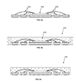
- FIG. 2 a shows a region on a planar side of a lead frame onto which semiconductor dies are bonded according to a preferred embodiment of the invention
- FIG. 2 b shows a cross-sectional view of the region on the lead frame.
- the region on the planar side of the lead frame as shown in FIG. 2 a defines leads 206 and a die-attach pad 208 .
- the leads 206 are arranged in inner and outer rings to increase the density of electrical interconnections within the lead frame, and are electrically insulated from the die-attach pad 208 via a non-conductive filling compound 306 to form a plurality of separate conductive regions on the planar side of the lead frame.
- bonding wires are used to form electrical interconnections between the semiconductor die and the leads 206 of the die-attach region 204 .
- the leads 206 of the die-attach region 204 includes a fine pitch configuration, wherein the pitch distance between adjacent leads 206 measures about 90 microns.
- the conductive regions are operative to electrically connect the semiconductor die to corresponding conductive pads on a printed circuit board (PCB).
- FIG. 2 b shows a cross-sectional view of the region of the lead frame. It can be seen that the plurality of conductive regions comprising the leads 206 and the die-attach pad 208 each has a larger surface area than its corresponding conductive contact 209 on an opposite planar side of the lead frame. Such a configuration provides strong mechanical interlocking which improves the pull strength of the leads 206 and the die-attach pad 208 , and properly secures the leads 206 and the die-attach pad 208 inside an encapsulation mold when the final semiconductor package has been formed.
- the overall package reliability of a final semiconductor package can be improved.
- FIGS. 3 a - 3 e show the steps of fabricating the lead frame according to a first embodiment of the invention.
- an electrically-conductive base material 300 having first and second planar sides 300 a , 300 b is provided as shown in FIG. 3 a .
- the conductive base material 300 is a copper alloy having a thickness of about 4 to 20 mils (i.e. about 0.1 mm to 0.5 mm). It should, however, be appreciated that the base material 300 may also comprise other types of metallic alloy so long as they are electrically conductive.
- photoresist layers 305 a , 305 b are coated on the first and second planar sides 300 a , 300 b respectively.
- the photoresist layers 305 a , 305 b comprise openings 307 a , 307 b on the first and second planar sides 300 a , 300 b of the base material 300 at positions corresponding to the patterned conductive layer 204 and the conductive contacts 209 of the lead frame respectively.
- Each of the photoresist layers 305 a , 305 b may be formed by first coating uniform photoresist layers on the first and second planar sides 300 a , 300 b by lamination, screen-printing or spin-coating.
- required images corresponding to the patterned conductive layer 204 and the conductive contacts 209 are imprinted on the uniform photoresist layers using UV radiation, so as to remove portions of the uniform photoresist layers corresponding to the patterned conductive layer 204 and the conductive contacts 209 to form suitable photoresist masks.
- the patterned conductive layer 204 and the conductive contacts 209 are thereby formed in the openings 307 a , 307 b of the photoresist layers 305 a , 305 b on the first and second planar side 300 a , 300 b of the conductive base material 300 , as shown in FIG. 3 b .
- the photoresist layers 305 a , 305 b are then removed from the base material 300 . Removal of the photoresist layers 305 a , 305 b may be accomplished by way of aqueous dissolution in an alkaline solution.
- the patterned conductive layer 204 and the conductive contacts may comprise any conductive material that is suitable for wire bonding and soldering. Examples of suitable conductive materials include Silver (Ag), Nickel-Palladium-Gold (Ni—Pd—Au) alloy, and Nickel-Silver alloy (Ni—Ag).
- the patterned conductive layer 204 and the conductive contacts 209 may also be formed by printing a conductive material, such as copper paste or copper ink, directly on the desired portions of the first and second planar sides 300 a , 300 b of the base material 300 , followed by a curing or sintering process to allow the conductive material to solidify.
- a conductive material such as copper paste or copper ink
- the exposed portions of the second planar side 300 b of the base material 300 comprising the conductive contacts 209 are etched through using an etching solution, such as cupric chloride, ferric chloride, or an ammonia-based alkaline, to form partially-etched portions 309 on the second planar side 300 b of the base material 300 , as shown in FIG. 3 c .
- an etching solution such as cupric chloride, ferric chloride, or an ammonia-based alkaline
- the etching depth of the second planar side 300 b of the base material 300 is controlled at more than 60% of the base material thickness to form the partially-etched portions 309 which are generally dome-shaped.
- Such an etched depth of the partially-etched portions 309 enhances structural support of the base material 300 because a sufficiently large volume of the non-conductive filling compound 306 can be filled therein.
- the dome-shaped of the partially-etched portions 309 also enhances structural support of the base material 300 when the conductive filling compound 307 is introduced therein.
- the non-conductive filling compound 306 is provided over the second planar side 300 b of the base material 300 such that the filling compound 306 fills the spaces inside the partially-etched portions 309 to form adjacent portions of the filling material 306 and the conductive contacts 209 on the second planar side 300 b of the base material 300 , as shown in FIG. 3 d .
- the filling compound 306 is preferably a thermoset type of plastic molding compound that is commonly used in the semiconductor packaging industry.
- the filling compound 306 may comprise any material (e.g. an epoxy molding compound) so long as it is not electrically conductive.
- the step of providing the filling compound 306 over the second planar side 300 b of the base material 300 may involve allowing the filling compound 306 to overflow from the partially-etched portions 309 , whereby a thickness of the filling compound 306 that overflows from the partially-etched portions 309 is about 4 mils (about 0.1 mm). However, it should be appreciated that the filling compound 306 may also overflow from the partially-etched portions 309 by any predetermined thickness. Deflashing of the filling compound 306 by either chemical deflashing or mechanical deflashing (e.g. grinding) is then carried out to remove the excess filling compound 306 , such that the conductive contacts 209 are exposed from the second planar side 300 b of the base material 300 as shown in FIG. 3 d.
- the exposed portions of the first planar side 300 a of the base material 300 comprising the patterned conductive layer 204 are etched through using an etching solution, such as cupric chloride, ferric chloride, or an ammonia-based alkaline, to form partially-etched portions 311 that are generally dome-shaped on the first planar side 300 a of the base material 300 , as shown in FIG. 3 e .
- an etching solution such as cupric chloride, ferric chloride, or an ammonia-based alkaline
- the partially-etched portions 311 on the first planar side 300 a of the base material 300 combine with the respective partially-etched portions 309 on the second planar side 300 b of the base material 300 , to form a plurality of separate conductive regions on the first planar side 300 a of the base material 300 which define the leads 206 and the die-attach pads 208 .
- each conductive region is electrically conductive with at least a respective one of the conductive contacts 209 on the second planar side 300 b of the base material 300 .
- FIGS. 4 a - 4 f show the steps of fabricating the lead frame according to a second embodiment of the invention.
- the electrically-conductive base material 300 having the first and second planar sides 300 a , 300 b is first provided, before the photoresist layers 305 a , 305 c are coated on the first and second planar sides 300 a , 300 b of the base material 300 respectively.
- a masking layer 401 is provided over the second planar side 300 b of the base material 300 for protection (see FIG. 4 b ), before the patterned conductive layer 204 is formed on the first planar side 300 a of the base material 300 .
- the masking material 401 may be a tape or any other suitable non-conductive protective material.
- the masking layer 401 is then removed (see FIG. 4 c ). Subsequently, the exposed portions of the second planar side 300 b of the base material 300 comprising the photoresist layer 305 c are etched through to form the partially-etched portions 309 before the photoresist layer 305 c on the second planar side 300 b of the base material 300 is removed (see FIG. 4 d ).
- the non-conductive filling compound 306 is provided over the second planar side 300 b of the base material 300 such that the filling compound 306 fills the spaces inside the partially-etched portions 309 (see FIG. 4 e ).
- the exposed portions of the first planar side 300 a of the base material 300 comprising the patterned conductive layer 204 are etched through to form the partially-etched portions 311 on the first planar side 300 a of the base material 300 (see FIG. 4 f ).
- the partially-etched portions 311 on the first planar side 300 a of the base material 300 combine with the respective partially-etched portions 309 on the second planar side 300 b of the base material 300 , to form a plurality of separate conductive regions on the first planar side 300 a of the base material 300 which define the leads 206 and the die-attach pads 208 .
- each conductive region is electrically conductive with at least a respective one of the conductive contacts 209 on the second planar side 300 b of the base material 300 .
- the second planar side 300 a of the base material 300 is plated (not shown) to form the conductive contacts 209 and the fabrication of the lead frame is completed.
- the filling material inside the partially-etched portions 309 on the second planar side 300 b of the base material 300 serves as a mask for plating the conductive portions 209 on the second planar side of the base material 300 , and therefore, a separate photoresist mask would not be required.
- the filling material 306 on the second planar side 300 b of the base material 300 can act as a photoresist layer for plating the second planar side 300 a of the base material 300 to form the conductive contacts 209 . It should also be appreciated that similar processes of the first embodiment of the invention as described above also apply to the second embodiment of the invention.
- FIGS. 5 a - 5 e show the steps of fabricating the lead frame according to a third embodiment of the invention.
- the electrically-conductive base material 300 having the first and second planar sides 300 a , 300 b is first provided, before the photoresist layers 305 a , 305 d are coated on the first and second planar sides 300 a , 300 b of the base material 300 respectively (see FIG. 5 a ).
- the photoresist layer 305 d on the second planar side 300 b of the base material 300 is a uniform layer of photoresist layer.
- the photoresist layer 305 c on the second planar side 300 b of the base material 300 is subject to UV radiation to form the photoresist layer 305 c (see FIG. 5 b ).
- the exposed portions of the second planar side 300 b of the base material 300 comprising the photoresist layer 305 c are etched through to form the partially-etched portions 309 before the photoresist layer 305 c on the second planar side 300 b of the base material 300 is removed (see FIG. 5 c ).
- the non-conductive filling compound 306 is provided over the second planar side 300 b of the base material 300 such that the filling compound 306 fills the spaces inside the partially-etched portions 309 (see FIG. 5 d ).
- the exposed portions of the first planar side 300 a of the base material 300 comprising the patterned conductive layer 204 are etched through to form the partially-etched portions 311 on the first planar side 300 a of the base material 300 (see FIG. 5 e ).
- the partially-etched portions 311 on the first planar side 300 a of the base material 300 combine with the respective partially-etched portions 309 on the second planar side 300 b of the base material 300 , to form a plurality of separate conductive regions on the first planar side 300 a of the base material 300 which define the leads 206 and the die-attach pads 208 .
- each conductive region is electrically conductive with at least a respective one of the conductive contacts 209 on the second planar side 300 b of the base material 300 .
- the second planar side 300 a of the base material 300 is plated (not shown) to form the conductive contacts 209 and the fabrication of the lead frame is completed.
- the filling material 306 on the second planar side 300 b of the base material 300 can act as a photoresist layer for plating the second planar side 300 a of the base material 300 to form the conductive contacts 209 . It should also be appreciated that similar processes of the first embodiment of the invention as described above also apply to the third embodiment of the invention.
- FIGS. 6 a - 6 c show the steps of fabricating the final semiconductor package structure using the lead frame.
- FIG. 4 a shows a semiconductor die 400 attached to the die-attach pad 208 via die bonding. Electrical connections are also formed between the semiconductor die 400 and the respective leads 206 of the lead frame via wire bonding using bonding wires 403 .
- FIG. 6 b shows the semiconductor die 400 being encapsulated by an encapsulant 405 (e.g. an epoxy molding compound), preferably by injection molding or compression molding, to form a final semiconductor package structure 402 .
- FIG. 6 c shows the final semiconductor package structure 402 being separated from the lead frame, preferably by a singulation process.
- an encapsulant 405 e.g. an epoxy molding compound
- the lead frame comprises regions onto which semiconductor dies are respectively bonded thereto. These regions may be in arranged in multiple arrays, each array comprising multiple rows and columns of individual regions onto which individual semiconductor dies (not shown) are bonded thereto.
Landscapes
- Lead Frames For Integrated Circuits (AREA)
- Physics & Mathematics (AREA)
- Geometry (AREA)
Abstract
Description
Claims (10)
Priority Applications (1)
| Application Number | Priority Date | Filing Date | Title |
|---|---|---|---|
| US14/158,321 US9202712B2 (en) | 2013-01-24 | 2014-01-17 | Lead frame and a method of manufacturing thereof |
Applications Claiming Priority (2)
| Application Number | Priority Date | Filing Date | Title |
|---|---|---|---|
| US201361756111P | 2013-01-24 | 2013-01-24 | |
| US14/158,321 US9202712B2 (en) | 2013-01-24 | 2014-01-17 | Lead frame and a method of manufacturing thereof |
Publications (2)
| Publication Number | Publication Date |
|---|---|
| US20140203418A1 US20140203418A1 (en) | 2014-07-24 |
| US9202712B2 true US9202712B2 (en) | 2015-12-01 |
Family
ID=51207087
Family Applications (1)
| Application Number | Title | Priority Date | Filing Date |
|---|---|---|---|
| US14/158,321 Active US9202712B2 (en) | 2013-01-24 | 2014-01-17 | Lead frame and a method of manufacturing thereof |
Country Status (2)
| Country | Link |
|---|---|
| US (1) | US9202712B2 (en) |
| SG (1) | SG2014004857A (en) |
Families Citing this family (5)
| Publication number | Priority date | Publication date | Assignee | Title |
|---|---|---|---|---|
| US9559077B2 (en) * | 2014-10-22 | 2017-01-31 | Nxp Usa, Inc. | Die attachment for packaged semiconductor device |
| KR101999594B1 (en) * | 2018-02-23 | 2019-10-01 | 해성디에스 주식회사 | Method for manufacturing semiconductor package substrate, semiconductor package substratemanufactured using the same, Method for manufacturing semiconductor package and semiconductor package manufactured using the same |
| CN112147270B (en) * | 2020-11-10 | 2022-04-12 | 佛山市南海正业建设工程质量检测有限公司 | Sampling and sample conveying device of energy-saving material monomer combustion testing machine |
| US20220157707A1 (en) * | 2020-11-17 | 2022-05-19 | Panjit International Inc. | Thin semiconductor package and manufacturing method thereof |
| CN117855147A (en) * | 2024-01-05 | 2024-04-09 | 山东瑞启微电子科技有限公司 | A thermally matched TMV carrier and a manufacturing method thereof |
Citations (7)
| Publication number | Priority date | Publication date | Assignee | Title |
|---|---|---|---|---|
| US20080061414A1 (en) * | 2006-08-30 | 2008-03-13 | United Test And Assembly Center Ltd. | Method of Producing a Semiconductor Package |
| US20090032943A1 (en) * | 2007-07-31 | 2009-02-05 | Seiko Epson Corporation | Substrate, substrate fabrication, semiconductor device, and semiconductor device fabrication |
| US20090283884A1 (en) * | 2008-05-16 | 2009-11-19 | Samsung Techwin Co., Ltd. | Lead frame, semiconductor package including the same, and method of manufacturing the lead frame and the semiconductor package |
| US20110267789A1 (en) | 2010-04-28 | 2011-11-03 | Advanpack Solutions Pte Ltd. | Etch-back type semiconductor package, substrate and manufacturing method thereof |
| US20120104588A1 (en) * | 2006-12-27 | 2012-05-03 | Nan-Jang Chen | Method for manufacturing leadframe, packaging method for using the leadframe and semiconductor package product |
| US20120241962A1 (en) * | 2011-03-24 | 2012-09-27 | Zigmund Ramirez Camacho | Integrated circuit packaging system with lead frame etching and method of manufacture thereof |
| US20130154072A1 (en) * | 2011-12-14 | 2013-06-20 | Byung Tai Do | Integrated circuit packaging system with pad and method of manufacture thereof |
-
2014
- 2014-01-17 US US14/158,321 patent/US9202712B2/en active Active
- 2014-01-21 SG SG2014004857A patent/SG2014004857A/en unknown
Patent Citations (7)
| Publication number | Priority date | Publication date | Assignee | Title |
|---|---|---|---|---|
| US20080061414A1 (en) * | 2006-08-30 | 2008-03-13 | United Test And Assembly Center Ltd. | Method of Producing a Semiconductor Package |
| US20120104588A1 (en) * | 2006-12-27 | 2012-05-03 | Nan-Jang Chen | Method for manufacturing leadframe, packaging method for using the leadframe and semiconductor package product |
| US20090032943A1 (en) * | 2007-07-31 | 2009-02-05 | Seiko Epson Corporation | Substrate, substrate fabrication, semiconductor device, and semiconductor device fabrication |
| US20090283884A1 (en) * | 2008-05-16 | 2009-11-19 | Samsung Techwin Co., Ltd. | Lead frame, semiconductor package including the same, and method of manufacturing the lead frame and the semiconductor package |
| US20110267789A1 (en) | 2010-04-28 | 2011-11-03 | Advanpack Solutions Pte Ltd. | Etch-back type semiconductor package, substrate and manufacturing method thereof |
| US20120241962A1 (en) * | 2011-03-24 | 2012-09-27 | Zigmund Ramirez Camacho | Integrated circuit packaging system with lead frame etching and method of manufacture thereof |
| US20130154072A1 (en) * | 2011-12-14 | 2013-06-20 | Byung Tai Do | Integrated circuit packaging system with pad and method of manufacture thereof |
Also Published As
| Publication number | Publication date |
|---|---|
| US20140203418A1 (en) | 2014-07-24 |
| SG2014004857A (en) | 2014-08-28 |
Similar Documents
| Publication | Publication Date | Title |
|---|---|---|
| US9281218B2 (en) | Method of producing a semiconductor package | |
| US9305868B2 (en) | Manufacturing method of forming an etch-back type semiconductor package with locking anchorages | |
| US9275972B2 (en) | Resin-encapsulated semiconductor device and method of manufacturing the same | |
| US7087461B2 (en) | Process and lead frame for making leadless semiconductor packages | |
| US7934313B1 (en) | Package structure fabrication method | |
| EP1235272B1 (en) | Leadframe, resin-molded semiconductor device including the leadframe, method of making the leadframe and method for manufacturing the device | |
| US9136247B2 (en) | Resin-encapsulated semiconductor device and method of manufacturing the same | |
| US20100258934A1 (en) | Advanced quad flat non-leaded package structure and manufacturing method thereof | |
| US8115288B2 (en) | Lead frame for semiconductor device | |
| US20090283884A1 (en) | Lead frame, semiconductor package including the same, and method of manufacturing the lead frame and the semiconductor package | |
| US10573590B2 (en) | Multi-layer leadless semiconductor package and method of manufacturing the same | |
| US9129975B2 (en) | Method of forming a thin substrate chip scale package device and structure | |
| CN109390237B (en) | Side solderable leadless package | |
| US9202712B2 (en) | Lead frame and a method of manufacturing thereof | |
| US9053968B2 (en) | Semiconductor package structure and manufacturing method thereof | |
| JP6505540B2 (en) | Semiconductor device and method of manufacturing semiconductor device | |
| US20080174981A1 (en) | Pre-molded lead frame and process for manufacturing the same | |
| KR20150005256A (en) | Lead frame using separated mold, method of manufacturing the same and semiconductor package, method of manufacturing the same | |
| US9805956B2 (en) | Lead frame and a method of fabrication thereof | |
| JP6676854B2 (en) | Lead frame, and method of manufacturing lead frame and semiconductor device | |
| KR101134706B1 (en) | Leadframe and method for manufacturing the same | |
| KR20090107671A (en) | Manufacturing method of lead frame | |
| KR101553470B1 (en) | Manufacturing method of semiconductor device and semiconductor device thereof | |
| JP2005302986A (en) | Semiconductor device, manufacturing method thereof, mounting structure thereof, and lead frame |
Legal Events
| Date | Code | Title | Description |
|---|---|---|---|
| AS | Assignment |
Owner name: ASM TECHNOLOGY SINGAPORE PTE LTD, SINGAPORE Free format text: ASSIGNMENT OF ASSIGNORS INTEREST;ASSIGNORS:XING, DAWEI;LIU, JIE;GUAN, HONG WEI;AND OTHERS;REEL/FRAME:032321/0107 Effective date: 20140117 |
|
| STCF | Information on status: patent grant |
Free format text: PATENTED CASE |
|
| FEPP | Fee payment procedure |
Free format text: SURCHARGE FOR LATE PAYMENT, LARGE ENTITY (ORIGINAL EVENT CODE: M1554); ENTITY STATUS OF PATENT OWNER: LARGE ENTITY |
|
| MAFP | Maintenance fee payment |
Free format text: PAYMENT OF MAINTENANCE FEE, 4TH YEAR, LARGE ENTITY (ORIGINAL EVENT CODE: M1551); ENTITY STATUS OF PATENT OWNER: LARGE ENTITY Year of fee payment: 4 |
|
| AS | Assignment |
Owner name: ADVANCED ASSEMBLY MATERIALS INTERNATIONAL LIMITED, HONG KONG Free format text: NUNC PRO TUNC ASSIGNMENT;ASSIGNOR:ASM TECHNOLOGY SINGAPORE PTE. LTD.;REEL/FRAME:056335/0646 Effective date: 20201201 |
|
| MAFP | Maintenance fee payment |
Free format text: PAYMENT OF MAINTENANCE FEE, 8TH YEAR, LARGE ENTITY (ORIGINAL EVENT CODE: M1552); ENTITY STATUS OF PATENT OWNER: LARGE ENTITY Year of fee payment: 8 |