US9176513B2 - High dynamic range exponential current generator with MOSFETs - Google Patents
High dynamic range exponential current generator with MOSFETs Download PDFInfo
- Publication number
- US9176513B2 US9176513B2 US14/243,741 US201414243741A US9176513B2 US 9176513 B2 US9176513 B2 US 9176513B2 US 201414243741 A US201414243741 A US 201414243741A US 9176513 B2 US9176513 B2 US 9176513B2
- Authority
- US
- United States
- Prior art keywords
- current
- current generator
- circuit
- single quadrant
- aspect ratio
- Prior art date
- Legal status (The legal status is an assumption and is not a legal conclusion. Google has not performed a legal analysis and makes no representation as to the accuracy of the status listed.)
- Expired - Fee Related, expires
Links
- 230000002457 bidirectional effect Effects 0.000 claims 2
- 238000005516 engineering process Methods 0.000 abstract description 7
- 238000004088 simulation Methods 0.000 description 7
- 238000010586 diagram Methods 0.000 description 6
- 238000000034 method Methods 0.000 description 6
- 238000013461 design Methods 0.000 description 2
- 230000000694 effects Effects 0.000 description 2
- 230000001052 transient effect Effects 0.000 description 2
- 239000008186 active pharmaceutical agent Substances 0.000 description 1
- 230000003466 anti-cipated effect Effects 0.000 description 1
- 238000013459 approach Methods 0.000 description 1
- FMWLUWPQPKEARP-UHFFFAOYSA-N bromodichloromethane Chemical compound ClC(Cl)Br FMWLUWPQPKEARP-UHFFFAOYSA-N 0.000 description 1
- 238000012552 review Methods 0.000 description 1
- 230000035945 sensitivity Effects 0.000 description 1
- 238000012546 transfer Methods 0.000 description 1
Images
Classifications
-
- G—PHYSICS
- G05—CONTROLLING; REGULATING
- G05F—SYSTEMS FOR REGULATING ELECTRIC OR MAGNETIC VARIABLES
- G05F3/00—Non-retroactive systems for regulating electric variables by using an uncontrolled element, or an uncontrolled combination of elements, such element or such combination having self-regulating properties
- G05F3/02—Regulating voltage or current
- G05F3/08—Regulating voltage or current wherein the variable is dc
- G05F3/10—Regulating voltage or current wherein the variable is dc using uncontrolled devices with non-linear characteristics
- G05F3/16—Regulating voltage or current wherein the variable is dc using uncontrolled devices with non-linear characteristics being semiconductor devices
- G05F3/20—Regulating voltage or current wherein the variable is dc using uncontrolled devices with non-linear characteristics being semiconductor devices using diode- transistor combinations
- G05F3/26—Current mirrors
- G05F3/262—Current mirrors using field-effect transistors only
Definitions
- the present invention relates to exponential generator circuits, and particularly to a high dynamic range exponential current generator utilizing MOSFETS operating in the weak inversion mode.
- An exponential function generator produces an output waveform (current/voltage) which is an exponential function of the input waveform (current/voltage).
- the exponential characteristics can be easily obtained in BiCMOS or Bipolar technologies using the intrinsic characteristics (I C /V BE ) of the bipolar transistors. Though, it is not easy to realize such function in CMOS technology because of the inherent square-law or linear characteristics of MOSFETs operating in the strong inversion region. So the widely used technique to implement analog exponential function circuits using MOSFETs in strong inversion is based on pseudo-approximations.
- a MOSFET device biased in weak inversion region is a well-known approach to introduce an exponential function due to the exponential relationship between I DS and V GS of MOSFET in weak inversion regime.
- I DS /V gs relationship the drain current of MOSFET in weak inversion region is given by:
- I DS 2 ⁇ n ⁇ ⁇ ⁇ n ⁇ C ox ⁇ W L ⁇ V T 2 ⁇ e ( V gs - V th nU T )
- the high dynamic range exponential current generator produces an output waveform (current/voltage) which is an exponential function of the input waveform (current/voltage).
- the exponential characteristics are obtained in BiCMOS or Bipolar technologies using the intrinsic characteristics (I C /V BE ) of the bipolar transistors.
- the high dynamic range exponential current generator is biased in weak inversion region. MOSFETs biased in weak inversion region are used not to utilize the inherent exponential (I DS /V GS ) relationship but to simply implement x 2 and x 4 terms using translinear loops.
- the term x 4 is realized by two cascaded squaring units. The approximation equation used is
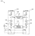
- FIG. 1 is a block diagram of the high dynamic range exponential current generator according to the present invention.
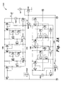
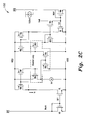
- FIGS. 2A-2C is a circuit diagram of the high dynamic range exponential current generator according to the present invention.
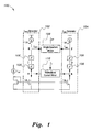
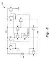
- FIG. 3 is a circuit diagram of a squaring unit of the high dynamic range exponential current generator according to the present invention.
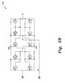
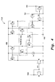
- FIG. 4 is a circuit diagram of a single quadrant divider of the high dynamic range exponential current generator according to the present invention.
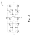
- FIG. 5 is a circuit diagram of a current mirror of the high dynamic range exponential current generator according to the present invention.
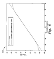
- FIG. 6 is a plot showing exact vs. proposed exponential approximation according to the present invention.
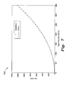
- FIG. 7 is a plot showing exact vs. simulation results of the SQ block of the high dynamic range exponential current generator according to the present invention.
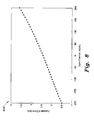
- FIG. 8 is a plot showing BDCM error of the high dynamic range exponential current generator according to the present invention.
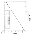
- FIG. 9 is a plot showing effect of mismatch in the current mirror of the high dynamic range exponential current generator according to the present invention.
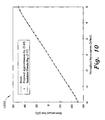
- FIG. 10 is a plot showing linear-in-dB characteristics of the high dynamic range exponential current generator according to the present invention.
- the high dynamic range exponential current generator produces an output waveform (current/voltage) which is an exponential function of the input waveform (current/voltage).
- the exponential characteristics are obtained in BiCMOS or Bipolar technologies using the intrinsic characteristics (I C /V BE ) of the bipolar transistors.
- the high dynamic range exponential current generator is biased in weak inversion region. MOSFETs biased in weak inversion region are used to simply implement x 2 and x 4 terms using translinear loops.
- the term x 4 is realized by two cascaded squaring units 106 .
- the exponential function generator approximation equation used is characterized by the relation,
- Plot 700 of FIG. 7 shows exact vs. simulation results of the squaring unit 106 .
- FIGS. 2A-2C The full block diagram of the present high dynamic range exponential current generator with MOSFETs 100 is shown in FIGS. 2A-2C .
- the number of transistors used in the overall circuit is 65 MOSFETs without any passive elements and all of them are stacked between ⁇ 0.75V voltage-supply.
- the squaring unit 106 is shown in detail in FIG. 3 .
- the voltage supply is ⁇ 0.75V and the aspect ratios of the transistors are illustrated in Table 1.
- the constant currents equal to 4 I ref and 1.6 I ref can be easily provided by a proper current source and current sink of current I ref ; e.g. if the current I ref shown in FIG. 1 is set to be 25 nA, then the constant current 4 I ref flowing through M9 (shown in FIG. 3 ) will be 100 nA.
- Equation (4) represents the current-mode squaring function. Since the squaring circuit 106 is a key block in the present current-mode exponential generator 100 , the simulation results have been carried out to demonstrate the validity of the theory. The corresponding maximum error is 1.5% and the circuit is stable with temperature variation. Table 1 details the aspect ratios of the squaring unit.
- the transistors involved in dashed box Ma-Md forms a single-quadrant current divider where all transistors are operating in the sub-threshold region.
- the current mirror circuitry (CM) 110 has two output currents. If the input current is I x then two copies of this current can obtained at the output, I x and ⁇ I x .
- the dimensions of CM 110 are listed in Table 3. The simulation results with ⁇ 0.75V voltage supply are shown to verify the functionality of the circuit. Plot 600 of FIG. 6 shows exact vs. the present exponential approximation. With respect to the DC transfer characteristics and transient response, the calculated error is very small, as shown in plot 800 of FIG. 8 .
- the full circuit of the present current-mode exponential function generator (EXPFG) 100 is shown in FIGS. 2A-2C .
- the EXPFG Circuit 100 shown in detail in FIGS. 2A-2C is used to implement the present function and is verified by simulation in 0.35 ⁇ m CMOS process technology with supply voltage ⁇ 0.75V.
- the threshold voltage of PMOS and NMOS is 0.833V and 0.572V in this process technology.
- the Tanner simulation result is illustrated in plot 1000 of FIG. 10 where I ref equals to 25 nA.
- the x-axis, 150 nA ⁇ I x ⁇ 150 nA can be normalized as ⁇ 6 ⁇ x ⁇ 6 for comparison purposes.
- the curve of the present function is very close to the ideal exponential function
- I w ⁇ e ( I x 25 ⁇ ⁇ ⁇ nA ) is limited to ⁇ 0.5 dB when ⁇ 137.5 nA ⁇ I x ⁇ 137.5 nA.
Abstract
Description
and has a dynamic range of approximately 96 dB.
V gs1 +V gs2 =V gs3 +V gs4, (2)
where Vgs1, Vgs2, Vgs3 and Vgs4 are the gate-to-source voltages of M1, M2, M3 and M4 respectively. From equation (2), one obtains the following:
I 1 I 2 =I 3 I 4. (3)
Since I1=I2=Ix, I3=4Iref and I4=Iout then the output current will be expressed as follows:
Equation (4) represents the current-mode squaring function. Since the
| TABLE 1 |
| Aspect ratios of squaring unit |
| Transistor |
|
Ratio |
| M1, M3 | 3.5/7 | 0.5 |
| M2, M4 | 91.7/7 | 13.1 |
| M5-M10 | 7/7 | 1 |
V sga +V sgb =V sgc +V sgd, (5)
I a I b =I c I d, (6)
with Ia=Iw, Ib=0.125 Inum, Ic=0.125 Iden, and Id=Iout. Then the equation (6) becomes
The transistor ratios are shown in Table 2. The
scale down the currents Inum and Iden so that transistors Mb (representing the dividend quantity) and Mc (representing the divisor quantity) can absorb this amount of current and as a result the quotient amount (represented by Md) can be improved in terms of accuracy. This implies that the aspect ratios of all the transistors involved in the translinear loop must be selected to meet the anticipated dynamic range of the input and output currents. Table 2 details the transistor dimensions of the single
| TABLE 2 |
| Transistor dimensions of the single quadrant divider circuit |
| Transistor |
|
Ratio |
| Ma, Md | 196/1.4 | 140 |
| Mb, Md | 175/1.4 | 125 |
| Me-Mh | 7/7 | 1 |
| Mi, Mk | 19.6/19.6 | 1 |
| Mj, Ml | 2.45/19.6 | 0.125 |
| Mm- |
1/1 | 1 |
| TABLE 3 |
| Dimensions of CM |
| Transistor | | Ratio |
| Mn1- | 1/10 | 0.1 |
| Mp1-Mp5 | 1.7/10 | 0.17 |
With reference to the present current mode
By recall of the equations, the output current of the present EXPFG will be
where Iout is the output current, Ix is the input ac signal, Iref is a constant current and Iw is a DC component which can be used to scale the output signal. From equation (17), it is clear that the exponential current-mode generator can be realized and its output current can be adjusted by Iw. The full circuit of the present current-mode exponential function generator (EXPFG) 100 is shown in
where
Assuming that there is ±10% deviation from the exact value (0.025), the results shown in
with a high output dynamic range, nearly 96 dB. The error between the present function and the ideal exponential function,
is limited to ±0.5 dB when −137.5 nA≦Ix≦137.5 nA.
Claims (4)
Priority Applications (1)
| Application Number | Priority Date | Filing Date | Title |
|---|---|---|---|
| US14/243,741 US9176513B2 (en) | 2014-04-02 | 2014-04-02 | High dynamic range exponential current generator with MOSFETs |
Applications Claiming Priority (1)
| Application Number | Priority Date | Filing Date | Title |
|---|---|---|---|
| US14/243,741 US9176513B2 (en) | 2014-04-02 | 2014-04-02 | High dynamic range exponential current generator with MOSFETs |
Publications (2)
| Publication Number | Publication Date |
|---|---|
| US20150286237A1 US20150286237A1 (en) | 2015-10-08 |
| US9176513B2 true US9176513B2 (en) | 2015-11-03 |
Family
ID=54209708
Family Applications (1)
| Application Number | Title | Priority Date | Filing Date |
|---|---|---|---|
| US14/243,741 Expired - Fee Related US9176513B2 (en) | 2014-04-02 | 2014-04-02 | High dynamic range exponential current generator with MOSFETs |
Country Status (1)
| Country | Link |
|---|---|
| US (1) | US9176513B2 (en) |
Families Citing this family (1)
| Publication number | Priority date | Publication date | Assignee | Title |
|---|---|---|---|---|
| CN108563277B (en) * | 2018-06-11 | 2020-04-17 | 北京工业大学 | Exponential waveform current generation circuit based on CMOS |
Citations (8)
| Publication number | Priority date | Publication date | Assignee | Title |
|---|---|---|---|---|
| US6744319B2 (en) | 2001-12-13 | 2004-06-01 | Hynix Semiconductor Inc. | Exponential function generator embodied by using a CMOS process and variable gain amplifier employing the same |
| US6882185B1 (en) | 1998-07-02 | 2005-04-19 | Qualcomm, Incorporated | Exponential current generator and method |
| US7180358B2 (en) | 2003-12-26 | 2007-02-20 | Electronics And Telecommunications Research Institute | CMOS exponential function generating circuit with temperature compensation technique |
| US7514980B2 (en) | 2005-06-23 | 2009-04-07 | Samsung Electro-Mechanics Co., Ltd. | Exponential function generator and variable gain amplifier using the same |
| US20100259317A1 (en) * | 2009-04-14 | 2010-10-14 | Chung Yuan Christian University | High-output-impedance current mirror |
| US7979036B2 (en) | 2004-12-30 | 2011-07-12 | Agency For Science, Technology And Research | Fully integrated ultra wideband transmitter circuits and systems |
| US20120081168A1 (en) * | 2010-10-01 | 2012-04-05 | Texas Instruments Incorporated A Delaware Corporation | Implementing a piecewise-polynomial-continuous function in a translinear circuit |
| US8305134B2 (en) | 2009-03-02 | 2012-11-06 | Semiconductor Technology Academic Research Center | Reference current source circuit provided with plural power source circuits having temperature characteristics |
-
2014
- 2014-04-02 US US14/243,741 patent/US9176513B2/en not_active Expired - Fee Related
Patent Citations (8)
| Publication number | Priority date | Publication date | Assignee | Title |
|---|---|---|---|---|
| US6882185B1 (en) | 1998-07-02 | 2005-04-19 | Qualcomm, Incorporated | Exponential current generator and method |
| US6744319B2 (en) | 2001-12-13 | 2004-06-01 | Hynix Semiconductor Inc. | Exponential function generator embodied by using a CMOS process and variable gain amplifier employing the same |
| US7180358B2 (en) | 2003-12-26 | 2007-02-20 | Electronics And Telecommunications Research Institute | CMOS exponential function generating circuit with temperature compensation technique |
| US7979036B2 (en) | 2004-12-30 | 2011-07-12 | Agency For Science, Technology And Research | Fully integrated ultra wideband transmitter circuits and systems |
| US7514980B2 (en) | 2005-06-23 | 2009-04-07 | Samsung Electro-Mechanics Co., Ltd. | Exponential function generator and variable gain amplifier using the same |
| US8305134B2 (en) | 2009-03-02 | 2012-11-06 | Semiconductor Technology Academic Research Center | Reference current source circuit provided with plural power source circuits having temperature characteristics |
| US20100259317A1 (en) * | 2009-04-14 | 2010-10-14 | Chung Yuan Christian University | High-output-impedance current mirror |
| US20120081168A1 (en) * | 2010-10-01 | 2012-04-05 | Texas Instruments Incorporated A Delaware Corporation | Implementing a piecewise-polynomial-continuous function in a translinear circuit |
Also Published As
| Publication number | Publication date |
|---|---|
| US20150286237A1 (en) | 2015-10-08 |
Similar Documents
| Publication | Publication Date | Title |
|---|---|---|
| US8760216B2 (en) | Reference voltage generators for integrated circuits | |
| US20180143659A1 (en) | Reference voltages | |
| Zeng et al. | A 12.8 nA and 7.2 ppm/° C CMOS voltage reference without amplifier | |
| US9176513B2 (en) | High dynamic range exponential current generator with MOSFETs | |
| US20150123724A1 (en) | Cmos current-mode square-root circuit | |
| US20160320790A1 (en) | Current mirror with tunable mirror ratio | |
| Petrović | A new tunable current-mode peak detector | |
| Danesh et al. | Ultra-low power analog multiplier based on translinear principle | |
| Yuce | Multiplier, frequency doubler and squarer circuits based on voltage controlled resistors | |
| Manhas et al. | High performance FGMOS-based low voltage current mirror | |
| US9634658B2 (en) | Apparatus and method for a self-biasing circuit for a FET passive mixer | |
| Pilipenko et al. | A Template Model of Junction Field-Effect Transistors for a Wide Temperature Range | |
| Ida et al. | MOS Reference Current Source Insensitive to Temperature Variation | |
| US8174308B2 (en) | DC slope generator | |
| US8841938B2 (en) | Voltage to current converter | |
| US20130328621A1 (en) | Semiconductor integrated circuit | |
| US10338616B2 (en) | Reference generation circuit | |
| Kuswan et al. | Temperature-Insensitive MOS Reference Current Source Circuit and its Startup Circuit | |
| Yue | A 46.468 µW low-power bandgap voltage reference | |
| JP4743795B2 (en) | Dual rail voltage generator | |
| Psychalinos et al. | Low-voltage reduced complexity cells for MOS translinear loops | |
| US20190334509A1 (en) | Self-compensated oscillator circuit | |
| Jie et al. | A chopper stabilized voltage reference using diode-connected MOS transistor | |
| Akshatha et al. | Low voltage, low power, high linearity, high speed CMOS voltage mode analog multiplier | |
| Maryan et al. | A High Linear Full-Wave Rectifier Based on Current Squarer Cell Using FGMOS Transistors |
Legal Events
| Date | Code | Title | Description |
|---|---|---|---|
| AS | Assignment |
Owner name: KING FAHD UNIVERSITY OF PETROLEUM AND MINERALS, SA Free format text: ASSIGNMENT OF ASSIGNORS INTEREST;ASSIGNORS:AL-ABSI, MUNIR A., DR.;AL-TAMIMI, KARAMA M., MR.;REEL/FRAME:032587/0262 Effective date: 20140101 |
|
| STCF | Information on status: patent grant |
Free format text: PATENTED CASE |
|
| MAFP | Maintenance fee payment |
Free format text: PAYMENT OF MAINTENANCE FEE, 4TH YR, SMALL ENTITY (ORIGINAL EVENT CODE: M2551); ENTITY STATUS OF PATENT OWNER: SMALL ENTITY Year of fee payment: 4 |
|
| FEPP | Fee payment procedure |
Free format text: MAINTENANCE FEE REMINDER MAILED (ORIGINAL EVENT CODE: REM.); ENTITY STATUS OF PATENT OWNER: SMALL ENTITY |
|
| LAPS | Lapse for failure to pay maintenance fees |
Free format text: PATENT EXPIRED FOR FAILURE TO PAY MAINTENANCE FEES (ORIGINAL EVENT CODE: EXP.); ENTITY STATUS OF PATENT OWNER: SMALL ENTITY |
|
| STCH | Information on status: patent discontinuation |
Free format text: PATENT EXPIRED DUE TO NONPAYMENT OF MAINTENANCE FEES UNDER 37 CFR 1.362 |
|
| FP | Lapsed due to failure to pay maintenance fee |
Effective date: 20231103 |