US9153888B2 - High speed flexible printed circuit connector - Google Patents
High speed flexible printed circuit connector Download PDFInfo
- Publication number
- US9153888B2 US9153888B2 US13/880,836 US201113880836A US9153888B2 US 9153888 B2 US9153888 B2 US 9153888B2 US 201113880836 A US201113880836 A US 201113880836A US 9153888 B2 US9153888 B2 US 9153888B2
- Authority
- US
- United States
- Prior art keywords
- actuator
- housing
- cavity
- electrical connector
- terminals
- Prior art date
- Legal status (The legal status is an assumption and is not a legal conclusion. Google has not performed a legal analysis and makes no representation as to the accuracy of the status listed.)
- Active, expires
Links
Images


Classifications
-
- H—ELECTRICITY
- H01—ELECTRIC ELEMENTS
- H01R—ELECTRICALLY-CONDUCTIVE CONNECTIONS; STRUCTURAL ASSOCIATIONS OF A PLURALITY OF MUTUALLY-INSULATED ELECTRICAL CONNECTING ELEMENTS; COUPLING DEVICES; CURRENT COLLECTORS
- H01R12/00—Structural associations of a plurality of mutually-insulated electrical connecting elements, specially adapted for printed circuits, e.g. printed circuit boards [PCB], flat or ribbon cables, or like generally planar structures, e.g. terminal strips, terminal blocks; Coupling devices specially adapted for printed circuits, flat or ribbon cables, or like generally planar structures; Terminals specially adapted for contact with, or insertion into, printed circuits, flat or ribbon cables, or like generally planar structures
- H01R12/70—Coupling devices
- H01R12/77—Coupling devices for flexible printed circuits, flat or ribbon cables or like structures
- H01R12/771—Details
- H01R12/774—Retainers
-
- H—ELECTRICITY
- H01—ELECTRIC ELEMENTS
- H01R—ELECTRICALLY-CONDUCTIVE CONNECTIONS; STRUCTURAL ASSOCIATIONS OF A PLURALITY OF MUTUALLY-INSULATED ELECTRICAL CONNECTING ELEMENTS; COUPLING DEVICES; CURRENT COLLECTORS
- H01R12/00—Structural associations of a plurality of mutually-insulated electrical connecting elements, specially adapted for printed circuits, e.g. printed circuit boards [PCB], flat or ribbon cables, or like generally planar structures, e.g. terminal strips, terminal blocks; Coupling devices specially adapted for printed circuits, flat or ribbon cables, or like generally planar structures; Terminals specially adapted for contact with, or insertion into, printed circuits, flat or ribbon cables, or like generally planar structures
- H01R12/70—Coupling devices
- H01R12/71—Coupling devices for rigid printing circuits or like structures
- H01R12/72—Coupling devices for rigid printing circuits or like structures coupling with the edge of the rigid printed circuits or like structures
-
- H—ELECTRICITY
- H01—ELECTRIC ELEMENTS
- H01R—ELECTRICALLY-CONDUCTIVE CONNECTIONS; STRUCTURAL ASSOCIATIONS OF A PLURALITY OF MUTUALLY-INSULATED ELECTRICAL CONNECTING ELEMENTS; COUPLING DEVICES; CURRENT COLLECTORS
- H01R12/00—Structural associations of a plurality of mutually-insulated electrical connecting elements, specially adapted for printed circuits, e.g. printed circuit boards [PCB], flat or ribbon cables, or like generally planar structures, e.g. terminal strips, terminal blocks; Coupling devices specially adapted for printed circuits, flat or ribbon cables, or like generally planar structures; Terminals specially adapted for contact with, or insertion into, printed circuits, flat or ribbon cables, or like generally planar structures
- H01R12/70—Coupling devices
- H01R12/77—Coupling devices for flexible printed circuits, flat or ribbon cables or like structures
- H01R12/79—Coupling devices for flexible printed circuits, flat or ribbon cables or like structures connecting to rigid printed circuits or like structures
-
- H—ELECTRICITY
- H01—ELECTRIC ELEMENTS
- H01R—ELECTRICALLY-CONDUCTIVE CONNECTIONS; STRUCTURAL ASSOCIATIONS OF A PLURALITY OF MUTUALLY-INSULATED ELECTRICAL CONNECTING ELEMENTS; COUPLING DEVICES; CURRENT COLLECTORS
- H01R12/00—Structural associations of a plurality of mutually-insulated electrical connecting elements, specially adapted for printed circuits, e.g. printed circuit boards [PCB], flat or ribbon cables, or like generally planar structures, e.g. terminal strips, terminal blocks; Coupling devices specially adapted for printed circuits, flat or ribbon cables, or like generally planar structures; Terminals specially adapted for contact with, or insertion into, printed circuits, flat or ribbon cables, or like generally planar structures
- H01R12/70—Coupling devices
- H01R12/82—Coupling devices connected with low or zero insertion force
- H01R12/85—Coupling devices connected with low or zero insertion force contact pressure producing means, contacts activated after insertion of printed circuits or like structures
- H01R12/88—Coupling devices connected with low or zero insertion force contact pressure producing means, contacts activated after insertion of printed circuits or like structures acting manually by rotating or pivoting connector housing parts
-
- H—ELECTRICITY
- H01—ELECTRIC ELEMENTS
- H01R—ELECTRICALLY-CONDUCTIVE CONNECTIONS; STRUCTURAL ASSOCIATIONS OF A PLURALITY OF MUTUALLY-INSULATED ELECTRICAL CONNECTING ELEMENTS; COUPLING DEVICES; CURRENT COLLECTORS
- H01R13/00—Details of coupling devices of the kinds covered by groups H01R12/70 or H01R24/00 - H01R33/00
- H01R13/646—Details of coupling devices of the kinds covered by groups H01R12/70 or H01R24/00 - H01R33/00 specially adapted for high-frequency, e.g. structures providing an impedance match or phase match
- H01R13/6461—Means for preventing cross-talk
- H01R13/6471—Means for preventing cross-talk by special arrangement of ground and signal conductors, e.g. GSGS [Ground-Signal-Ground-Signal]
-
- H—ELECTRICITY
- H01—ELECTRIC ELEMENTS
- H01R—ELECTRICALLY-CONDUCTIVE CONNECTIONS; STRUCTURAL ASSOCIATIONS OF A PLURALITY OF MUTUALLY-INSULATED ELECTRICAL CONNECTING ELEMENTS; COUPLING DEVICES; CURRENT COLLECTORS
- H01R13/00—Details of coupling devices of the kinds covered by groups H01R12/70 or H01R24/00 - H01R33/00
- H01R13/646—Details of coupling devices of the kinds covered by groups H01R12/70 or H01R24/00 - H01R33/00 specially adapted for high-frequency, e.g. structures providing an impedance match or phase match
- H01R13/6473—Impedance matching
- H01R13/6477—Impedance matching by variation of dielectric properties
-
- H—ELECTRICITY
- H01—ELECTRIC ELEMENTS
- H01R—ELECTRICALLY-CONDUCTIVE CONNECTIONS; STRUCTURAL ASSOCIATIONS OF A PLURALITY OF MUTUALLY-INSULATED ELECTRICAL CONNECTING ELEMENTS; COUPLING DEVICES; CURRENT COLLECTORS
- H01R13/00—Details of coupling devices of the kinds covered by groups H01R12/70 or H01R24/00 - H01R33/00
- H01R13/648—Protective earth or shield arrangements on coupling devices, e.g. anti-static shielding
- H01R13/658—High frequency shielding arrangements, e.g. against EMI [Electro-Magnetic Interference] or EMP [Electro-Magnetic Pulse]
- H01R13/6591—Specific features or arrangements of connection of shield to conductive members
- H01R13/6597—Specific features or arrangements of connection of shield to conductive members the conductive member being a contact of the connector
Definitions
- the present invention relates to an electrical connector, and more particularly to an electrical connector for connecting to a flexible printed circuit board.
- Flexible printed circuit (FPC) connectors are widely used in many electronic devices and systems for transmitting electrical signals.
- Conventional FPC connectors suffer signal integrity degradation and therefore are difficult to transmit signal in high speed.
- the present invention provides FPC connectors which are capable of transmitting signals in high speed and with improved signal integrity.
- a high speed flexible printed circuit (FPC) connector which includes a housing with ground and signal terminals arranged in the housing along a lateral direction.
- the housing has a cavity for receiving an FPC board therein.
- Each ground terminal has a first branch arm positioned adjacent to a bottom wall of the cavity and a second branch arm positioned adjacent to a top wall of the cavity.
- Each signal terminal is of a single, non-branched elongated shape and the signal terminals are positioned adjacent to the bottom wall of the cavity. Every two of the signal terminals are positioned adjacent to each other to form a signal terminal pair for differential signal transmission. Each signal pair is sandwiched between the first branch arms of two ground terminals.
- An actuator is coupled to the housing for fixing the FPC board in the cavity to establish electrical connections.
- the actuator may have recesses corresponding to the positions of the signal pairs to provide a dielectric constant different from that of the other parts of the actuator.
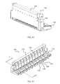
- FIG. 1 is a perspective front view of an FPC connector according to one embodiment of the present invention and to be connected to an FPC board;
- FIG. 2 is a perspective rear view of the connector shown in FIG. 1
- FIG. 3 is an exploded view of FIG. 2 ;
- FIG. 4 is a perspective view of a first type of contact terminal of the connector shown in FIG. 1 ;
- FIG. 5 is a perspective view of a second type of contact terminal of the connector shown in FIG. 1 ;
- FIG. 6 is a cross-sectional view of FIG. 2 along A-A;
- FIG. 7 is a cross-sectional view of FIG. 2 along B-B;
- FIG. 8 is a perspective view of FIG. 1 when the FPC board is connected to the connector;
- FIG. 9 is a cross-sectional view of FIG. 8 along C-C;
- FIG. 10 is a cross-sectional view of FIG. 8 along D-D;
- FIG. 11 is a perspective bottom view of FIG. 8 ;
- FIG. 12 is a partial enlarged view of FIG. 11 ;
- FIG. 13 is a partial cross sectional view of FIG. 12 ;
- FIG. 14 is a perspective front view of an FPC connector according to another embodiment of the present invention.
- FIG. 15 is a perspective rear view of FIG. 14 ;
- FIG. 16 is a perspective front view of FIG. 14 with the metal cover omitted;
- FIG. 17 is a cross-sectional view of FIG. 17 along E-E;
- FIG. 18 is a perspective view of FIG. 14 when an FPC board is connected to the connector;
- FIG. 19 is a cross-sectional view of FIG. 18 along F-F;
- FIG. 20 is a cross-sectional view of FIG. 18 along G-G.
- an FPC connector 100 includes a housing 110 and an actuator 120 pivotally attached to housing 110 .
- a plurality of first and second sets of terminals 130 and 140 are arranged in housing 110 .
- Housing 110 has a cavity 116 accessible from front end 102 of connector 100 . Cavity 116 is to allow insertion of an end portion of an FPC board 10 therein, by which an electrical connection can be established between FPC board 10 and connector 100 .
- An actuator 120 is coupled to housing 110 and supported by a pair of brackets 150 which are mounted to housing 110 .
- each of the first set of terminals 130 has a first branch arm 132 at lower side and second branch arm 134 at upper side.
- First and second branch arms 132 and 134 are connected integrally to a base portion 136 .
- first contact projection 132 a At distal end of first branch arm 132 there is formed a first contact projection 132 a .
- First branch arm 132 extends backwardly beyond base portion 136 , and forms a first tail portion 138 at the proximal end of first branch arm 132 .
- each of the second set of terminals 140 is of a generally elongated shape having a contact arm 142 . At distal end of contact arm 142 there is formed a second contact projection 142 a . At proximal end of contact arm 142 there is formed a second tail portion 148 .
- first set of terminals 130 (only one is shown) are fixed to housing 110 .
- First branch arm 132 of each of first set of terminals 130 is inserted into housing 110 through a first fixing slot 112 a .
- a front tip 137 of second branch arm 134 of each of first set of terminals 130 is inserted into a second fixing slot 114 of housing 110 .
- Actuator 120 is coupled to housing 110 with pivot 122 held to housing 110 by holding portion 135 formed on second branch arm 134 between tip 137 and base portion 136 of first contact terminals 130 .
- With the holding action provided by second branches 134 of first set of terminals 130 actuator 120 is prevented from being detached from housing 110 , but is allowed to rotate relative to housing 110 about pivot 122 .
- first branch arms 132 are positioned at a bottom side 116 a of cavity 116
- second branch arms 134 are positioned at a top side 116 b of cavity 116 .
- second set of terminals 140 (only one is shown) are fixed to housing 110 , with contact arm 142 inserted through a third fixing slot 112 b .
- second set of terminals 140 After being assembled to housing 110 , second set of terminals 140 are positioned at a bottom side 116 a of cavity 116 .
- both the first branch arms 132 of first set of terminals 130 and the second set of terminals 140 At top side 116 b , there are arranged only the second branch arms 134 of first set of terminals 130 .
- First branch arm 132 and contact arm 142 are now fixed to housing 110 in a cantilevered manner, hence first contact projection 132 a and second contact projection 142 a extend into, and become resiliently deflectable within, cavity 116 of housing 110 .
- the first set of terminals 130 are configured as ground terminals 130 for connector 100 , denoted in FIG. 2 as “GND (ground)” terminals. Every two of the second terminals 140 are positioned next to each other to form a signal contact pair 140 p , denoted in FIG. 2 as “S+” and “S ⁇ ” terminals for connector 100 , for transmission of a pair of differential signals.
- the ground terminals 130 and signal contact pairs 140 p are arranged in housing 110 in a staggered manner, i.e. each signal contact pair 140 p is sandwiched between two adjacent first branch arms 132 of ground terminals, as shown in FIG. 2 .
- FIGS. 8 , 9 and 10 when in use, the front end of an FPC board 10 is inserted into cavity 116 of housing 110 , and actuator 120 is rotated from a release position ( FIGS. 6 and 7 ) to a lock position ( FIGS. 8 , 9 and 10 ).
- a cam 124 formed on actuator 120 presses against top surface 14 of FPC board 10 , which causes bottom surface 12 of FPC board 10 to contact with contact projection 132 a of first branch arm 132 of each of the first set of terminals 130 , as well as contact projection 142 a of contact arm 142 of each of the second set of terminals 140 . Electrical connections can therefore be established between FPC board 10 and terminals 130 and 140 .
- second set of terminals 140 which serve as the signal contact terminals do not have any upper arm, as is the case of the first contact terminals 130 , the negative effects to signal integrity caused by conventional contact terminals having such upper arm, can be eliminated or at least substantially reduced. Only the first set of terminals 130 , which serve as ground contact terminals, have the upper arms which hold the actuator 120 to housing 110 and support the operation of actuator 120 . In this way, actuator 120 is allowed to rotate and can be prevented from being detached from housing 110 .
- Actuator 120 maybe formed with recesses 126 on its main plate 121 , as shown in FIGS. 2 , 11 , 12 and 13 .
- Recesses 126 are located such that when actuator 120 is at the lock position, each recess 126 overlaps one signal contact pair 140 p of second set of terminals 140 , providing an air gap 127 above each signal pair 140 p .
- Air gaps may be used to provide a dielectric constant (i.e. dielectric constant of air) different from that of the adjacent parts 128 (i.e. dielectric constant of the actuator material of e.g. plastic) of actuator 120 , to further improve the signal integrity, and to increase the signal transmission speed.
- actuator 120 maybe formed with grooves 129 on main plate 121 , as shown in FIGS. 2 , 3 and 9 .
- Each groove 129 is located between two adjacent recesses 126 and corresponding to the locations of second branch arm 134 of first set of terminals 130 .
- each of the second branch arms 134 of first set of terminals 130 is partially received into a corresponding groove 129 .
- grooves 129 can be useful to reduce the thickness of actuator and hence to reduce the overall thickness of connector 100 .
- voids 118 there may be formed air spaces in the form of voids 118 in housing 110 .
- the shape and dimension of voids 118 may vary, providing dielectric constant of air different from other part of housing 110 which are made of housing material, e.g. plastic. Voids 118 are therefore useful to further adjust the signal properties to match the signal transmission requirements.
- a connector 200 has a housing 210 and an actuator 220 pivotally attached to housing 210 .
- a plurality of first and second sets of terminals 230 and 240 are arranged in housing 210 , in a manner the same as that of the previous embodiment.
- Second set of terminals 240 which serve as signal contacts, have the same structure as that of the previous embodiment.
- first set of terminals 230 are structured differently, as illustrated below in further details.
- Connector 200 further includes a metal cover 250 coupled to housing 210 , to provide a shielding effect as well as an additional grounding effect to connector 200 .
- Metal cover 250 is rotatable relative to housing 210 between an open position ( FIG. 17 ) to allow actuator 220 to move to the release position, and a close position ( FIG. 19 ) to enclose actuator 220 when the actuator 220 is at the lock position.
- each of the first set of terminal 230 has a first branch arm 232 at lower side, with a contact projection 232 a at frond end (left side of FIG. 17 ) thereof, for contacting to an FPC board.
- Second branch arm 234 of first contact terminal 230 at upper side has a first projection 236 and a second projection 238 formed thereon.
- First projection 236 extends into cavity 216 towards lower arm 232 .
- Second projection 238 extends in an opposite direction from upper arm 234 .
- an FPC board 20 is inserted with its front end portion into cavity 216 of housing 210 , and actuator 220 is closed so as to fix FPC board 20 to housing 210 .
- Cam 224 of actuator 220 now presses against the top surface 24 of FPC board 20 which causes the bottom surface 22 to contact first contact protections 232 a of first set of terminals 230 as well as second contact projections 242 a of second set of terminals 240 .
- top surface 24 of FPC board 20 is brought into contact with first projection 236 to establish electrical connections between circuits 24 a (serving as ground-contacts) on top surface 24 of FPC board 20 and first contact terminal 230 .
- actuator 220 there are formed of a plurality of openings 228 ( FIG. 16 ) corresponding to the positions of second projections 238 such that, when actuator 220 is rotated to the lock position, as shown in FIG. 19 , second projections 238 pass though openings 228 and are accessible from top side of actuator 220 .
- each boss 258 is brought into contact with a respective second projection 238 of first set of terminals 230 .
- a grounding path is therefore established between ground circuit 24 a of FPC board 24 and metal cover, by the contact between ground circuit 24 a and first projection 236 , and the contact between second projection 238 and boss 258 of metal cover 250 . Grounding effect is further improved in this regard.
Landscapes
- Coupling Device And Connection With Printed Circuit (AREA)
- Details Of Connecting Devices For Male And Female Coupling (AREA)
Abstract
Description
Claims (20)
Applications Claiming Priority (4)
| Application Number | Priority Date | Filing Date | Title |
|---|---|---|---|
| IB2010003029 | 2010-10-22 | ||
| WOPCT/IB2010/003029 | 2010-10-22 | ||
| IBPCT/IB2010/003029 | 2010-10-22 | ||
| PCT/IB2011/002853 WO2012052845A2 (en) | 2010-10-22 | 2011-10-14 | High speed flexible printed circuit connector |
Related Parent Applications (1)
| Application Number | Title | Priority Date | Filing Date |
|---|---|---|---|
| PCT/IB2011/002853 A-371-Of-International WO2012052845A2 (en) | 2010-10-22 | 2011-10-14 | High speed flexible printed circuit connector |
Related Child Applications (1)
| Application Number | Title | Priority Date | Filing Date |
|---|---|---|---|
| US14/840,545 Continuation US9466903B2 (en) | 2010-10-22 | 2015-08-31 | High speed flexible printed circuit connector |
Publications (2)
| Publication Number | Publication Date |
|---|---|
| US20130267110A1 US20130267110A1 (en) | 2013-10-10 |
| US9153888B2 true US9153888B2 (en) | 2015-10-06 |
Family
ID=45975668
Family Applications (2)
| Application Number | Title | Priority Date | Filing Date |
|---|---|---|---|
| US13/880,836 Active 2032-04-04 US9153888B2 (en) | 2010-10-22 | 2011-10-14 | High speed flexible printed circuit connector |
| US14/840,545 Active US9466903B2 (en) | 2010-10-22 | 2015-08-31 | High speed flexible printed circuit connector |
Family Applications After (1)
| Application Number | Title | Priority Date | Filing Date |
|---|---|---|---|
| US14/840,545 Active US9466903B2 (en) | 2010-10-22 | 2015-08-31 | High speed flexible printed circuit connector |
Country Status (3)
| Country | Link |
|---|---|
| US (2) | US9153888B2 (en) |
| CN (1) | CN103477508A (en) |
| WO (1) | WO2012052845A2 (en) |
Cited By (7)
| Publication number | Priority date | Publication date | Assignee | Title |
|---|---|---|---|---|
| US20150311640A1 (en) * | 2014-04-28 | 2015-10-29 | Dai-Ichi Seiko Co., Ltd. | Electrical connector |
| US20160204533A1 (en) * | 2015-01-09 | 2016-07-14 | DAl-ICHI SEIKO CO., LTD. | Electric connector |
| US10069229B2 (en) * | 2016-12-09 | 2018-09-04 | Dai-Ichi Seiko Co., Ltd. | Electric connector |
| US10305209B2 (en) | 2016-02-26 | 2019-05-28 | Amphenol Fci Asia Pte Ltd | Electrical connector and method of assembling the same |
| US10530082B2 (en) | 2015-08-31 | 2020-01-07 | Amphenol Fci Asia Pte. Ltd. | Circuit board connector having a pair of locking arms |
| EP3736914A1 (en) * | 2019-05-08 | 2020-11-11 | Yamaichi Electronics Co., Ltd. | High frequency connector and flexible wiring board |
| US11289841B2 (en) * | 2018-07-27 | 2022-03-29 | Kyocera Corporation | Cable connector |
Families Citing this family (9)
| Publication number | Priority date | Publication date | Assignee | Title |
|---|---|---|---|---|
| JP6272660B2 (en) * | 2013-05-17 | 2018-01-31 | スリーエム イノベイティブ プロパティズ カンパニー | connector |
| JP6336941B2 (en) * | 2015-04-01 | 2018-06-06 | モレックス エルエルシー | Connector and manufacturing method thereof |
| JP6486477B2 (en) * | 2015-08-26 | 2019-03-20 | 京セラ株式会社 | connector |
| US10181670B2 (en) * | 2016-04-21 | 2019-01-15 | Te Connectivity Corporation | Connector sub-assembly and electrical connector having signal and ground conductors |
| US10847934B2 (en) * | 2016-09-22 | 2020-11-24 | Hewlett-Packard Development Company, L.P. | Electrical connectors for flat circuits |
| CN107919548B (en) * | 2016-10-11 | 2019-08-30 | 庆良电子股份有限公司 | Electric connector |
| KR102047680B1 (en) * | 2017-12-01 | 2019-12-02 | 히로세코리아 주식회사 | Connector for flexible cable |
| TWI753537B (en) * | 2020-08-17 | 2022-01-21 | 禾昌興業股份有限公司 | High-frequency connector with automatic locking structure |
| JP7438076B2 (en) | 2020-10-01 | 2024-02-26 | ヒロセ電機株式会社 | Mating electrical connector and electrical connector assembly |
Citations (16)
| Publication number | Priority date | Publication date | Assignee | Title |
|---|---|---|---|---|
| US5738545A (en) * | 1996-02-21 | 1998-04-14 | Japan Aviation Electronics Industry, Limited | Connection device which is electromagnetically shielded with simple structure |
| US6478612B2 (en) * | 1999-12-17 | 2002-11-12 | Fci Americas Technology, Inc. | Connector for a flat cable |
| WO2004030158A2 (en) | 2002-09-25 | 2004-04-08 | Molex Incorporated | Impedance-tuned terminal contact arrangement and connectors incorporating same |
| CN1515052A (en) | 2001-06-11 | 2004-07-21 | ��Ī������ | High-density impedance tuned connector |
| US6855002B2 (en) * | 2003-05-20 | 2005-02-15 | P-Two Industries, Inc. | Flat flexible circuit board connector |
| US20070004282A1 (en) | 2005-06-30 | 2007-01-04 | Teradyne, Inc. | High speed high density electrical connector |
| US20070032104A1 (en) | 2005-08-08 | 2007-02-08 | Ddk Ltd. | Electrical connector |
| JP2008053123A (en) | 2006-08-25 | 2008-03-06 | Jst Mfg Co Ltd | Fpc connector |
| JP2008186600A (en) | 2007-01-26 | 2008-08-14 | Kyocera Elco Corp | Connector |
| US20080220644A1 (en) | 2007-03-09 | 2008-09-11 | Kyocera Elco Corporation | Connector |
| US7637763B1 (en) * | 2008-08-15 | 2009-12-29 | Cheng Uei Precision Industry Co., Ltd. | Connector for flexible printed circuit |
| US7695311B2 (en) * | 2008-04-23 | 2010-04-13 | Japan Aviation Electronics Industry Limited | Connector |
| CN101859948A (en) | 2009-03-31 | 2010-10-13 | 广濑电机株式会社 | Electric connector for circuit substrate |
| US8025516B2 (en) * | 2009-06-02 | 2011-09-27 | Japan Aviation Electronics Industry, Limited | Connector having an actuator operable to hold a plate-like connection target between two metal abutment portions |
| US8622766B2 (en) * | 2009-10-01 | 2014-01-07 | Japan Aviation Electronics Industry, Limited | Connector |
| US8662915B2 (en) * | 2010-08-19 | 2014-03-04 | Japan Aviation Electronics Industry, Ltd. | Connector |
Family Cites Families (1)
| Publication number | Priority date | Publication date | Assignee | Title |
|---|---|---|---|---|
| AU2003234526A1 (en) * | 2002-05-06 | 2003-11-17 | Molex Incorporated | Terminal assemblies for differential signal connectors |
-
2011
- 2011-10-14 US US13/880,836 patent/US9153888B2/en active Active
- 2011-10-14 CN CN2011800546975A patent/CN103477508A/en active Pending
- 2011-10-14 WO PCT/IB2011/002853 patent/WO2012052845A2/en active Application Filing
-
2015
- 2015-08-31 US US14/840,545 patent/US9466903B2/en active Active
Patent Citations (18)
| Publication number | Priority date | Publication date | Assignee | Title |
|---|---|---|---|---|
| US5738545A (en) * | 1996-02-21 | 1998-04-14 | Japan Aviation Electronics Industry, Limited | Connection device which is electromagnetically shielded with simple structure |
| US6478612B2 (en) * | 1999-12-17 | 2002-11-12 | Fci Americas Technology, Inc. | Connector for a flat cable |
| CN1515052A (en) | 2001-06-11 | 2004-07-21 | ��Ī������ | High-density impedance tuned connector |
| WO2004030158A2 (en) | 2002-09-25 | 2004-04-08 | Molex Incorporated | Impedance-tuned terminal contact arrangement and connectors incorporating same |
| CN1742411A (en) | 2002-09-25 | 2006-03-01 | 莫莱克斯公司 | Impedance-tuned terminal contact arrangement and connectors incorporating same |
| US6855002B2 (en) * | 2003-05-20 | 2005-02-15 | P-Two Industries, Inc. | Flat flexible circuit board connector |
| CN101273501A (en) | 2005-06-30 | 2008-09-24 | 安费诺公司 | High speed, high density electrical connector |
| US20070004282A1 (en) | 2005-06-30 | 2007-01-04 | Teradyne, Inc. | High speed high density electrical connector |
| US20070032104A1 (en) | 2005-08-08 | 2007-02-08 | Ddk Ltd. | Electrical connector |
| JP2008053123A (en) | 2006-08-25 | 2008-03-06 | Jst Mfg Co Ltd | Fpc connector |
| JP2008186600A (en) | 2007-01-26 | 2008-08-14 | Kyocera Elco Corp | Connector |
| US20080220644A1 (en) | 2007-03-09 | 2008-09-11 | Kyocera Elco Corporation | Connector |
| US7695311B2 (en) * | 2008-04-23 | 2010-04-13 | Japan Aviation Electronics Industry Limited | Connector |
| US7637763B1 (en) * | 2008-08-15 | 2009-12-29 | Cheng Uei Precision Industry Co., Ltd. | Connector for flexible printed circuit |
| CN101859948A (en) | 2009-03-31 | 2010-10-13 | 广濑电机株式会社 | Electric connector for circuit substrate |
| US8025516B2 (en) * | 2009-06-02 | 2011-09-27 | Japan Aviation Electronics Industry, Limited | Connector having an actuator operable to hold a plate-like connection target between two metal abutment portions |
| US8622766B2 (en) * | 2009-10-01 | 2014-01-07 | Japan Aviation Electronics Industry, Limited | Connector |
| US8662915B2 (en) * | 2010-08-19 | 2014-03-04 | Japan Aviation Electronics Industry, Ltd. | Connector |
Cited By (9)
| Publication number | Priority date | Publication date | Assignee | Title |
|---|---|---|---|---|
| US20150311640A1 (en) * | 2014-04-28 | 2015-10-29 | Dai-Ichi Seiko Co., Ltd. | Electrical connector |
| US9966681B2 (en) * | 2014-04-28 | 2018-05-08 | Dai-Ichi Seiko Co., Ltd. | Electrical connector to sheild a transmission path |
| US20160204533A1 (en) * | 2015-01-09 | 2016-07-14 | DAl-ICHI SEIKO CO., LTD. | Electric connector |
| US9647365B2 (en) * | 2015-01-09 | 2017-05-09 | Dai-Ichi Seiko Co., Ltd. | Electric connector |
| US10530082B2 (en) | 2015-08-31 | 2020-01-07 | Amphenol Fci Asia Pte. Ltd. | Circuit board connector having a pair of locking arms |
| US10305209B2 (en) | 2016-02-26 | 2019-05-28 | Amphenol Fci Asia Pte Ltd | Electrical connector and method of assembling the same |
| US10069229B2 (en) * | 2016-12-09 | 2018-09-04 | Dai-Ichi Seiko Co., Ltd. | Electric connector |
| US11289841B2 (en) * | 2018-07-27 | 2022-03-29 | Kyocera Corporation | Cable connector |
| EP3736914A1 (en) * | 2019-05-08 | 2020-11-11 | Yamaichi Electronics Co., Ltd. | High frequency connector and flexible wiring board |
Also Published As
| Publication number | Publication date |
|---|---|
| US20130267110A1 (en) | 2013-10-10 |
| US9466903B2 (en) | 2016-10-11 |
| WO2012052845A2 (en) | 2012-04-26 |
| US20150372406A1 (en) | 2015-12-24 |
| CN103477508A (en) | 2013-12-25 |
| WO2012052845A3 (en) | 2014-03-27 |
Similar Documents
| Publication | Publication Date | Title |
|---|---|---|
| US9466903B2 (en) | High speed flexible printed circuit connector | |
| US11011874B2 (en) | Connector and connector assembly | |
| US9455530B2 (en) | Electrical connector with ground bus | |
| TWI523349B (en) | Electrical connector having contact modules | |
| JP6703900B2 (en) | Connectors and connector systems | |
| US7695311B2 (en) | Connector | |
| US11316304B2 (en) | Electrical connector with improved electrical performance | |
| US11283221B2 (en) | Connector | |
| US20110306244A1 (en) | Cable connector assembly having an adapter plate for grounding | |
| US7540784B1 (en) | Low profile electrical connector | |
| US7168985B1 (en) | Electrical connector assembly having an improved inner shield | |
| JP2011501358A (en) | Electrical connector assembly | |
| KR100904604B1 (en) | Multi-pole connector, and portable wireless terminal or compact electronic device using the multi-pole connector | |
| JP5966875B2 (en) | Connector and flexible printed circuit board | |
| TW200919842A (en) | Electrical connector | |
| JP2014531723A (en) | Electrical contacts and connectors | |
| CN109326906A (en) | It is in electrical contact pre-load arrangement | |
| KR20130039849A (en) | Connector assembly | |
| US20190052007A1 (en) | Signal transferring device and adapter assembly | |
| CN201178176Y (en) | Electric connector | |
| US10187988B1 (en) | Adapter with an insulating body having a circuit board with a plurality of conductive modules surface mounted on the board | |
| US20060211275A1 (en) | Card-edge board connector | |
| US20210336369A1 (en) | Machine case and cable connector assembly | |
| KR101170428B1 (en) | Connector for connecting flat cable | |
| KR101058699B1 (en) | Connector for connecting flat cable |
Legal Events
| Date | Code | Title | Description |
|---|---|---|---|
| AS | Assignment |
Owner name: FCI, FRANCE Free format text: ASSIGNMENT OF ASSIGNORS INTEREST;ASSIGNORS:KAJIURA, MOTOMU;SASAME, NAOTAKA;MOTOYAMA, MASASHIKO;SIGNING DATES FROM 20130502 TO 20130507;REEL/FRAME:030591/0785 |
|
| STCF | Information on status: patent grant |
Free format text: PATENTED CASE |
|
| AS | Assignment |
Owner name: FCI ASIA PTE. LTD., SINGAPORE Free format text: ASSIGNMENT OF ASSIGNORS INTEREST;ASSIGNOR:FCI;REEL/FRAME:037772/0686 Effective date: 20160208 |
|
| MAFP | Maintenance fee payment |
Free format text: PAYMENT OF MAINTENANCE FEE, 4TH YEAR, LARGE ENTITY (ORIGINAL EVENT CODE: M1551); ENTITY STATUS OF PATENT OWNER: LARGE ENTITY Year of fee payment: 4 |
|
| MAFP | Maintenance fee payment |
Free format text: PAYMENT OF MAINTENANCE FEE, 8TH YEAR, LARGE ENTITY (ORIGINAL EVENT CODE: M1552); ENTITY STATUS OF PATENT OWNER: LARGE ENTITY Year of fee payment: 8 |