US9147658B2 - Stacked power supplies for integrated circuit devices and methods of making the same - Google Patents
Stacked power supplies for integrated circuit devices and methods of making the same Download PDFInfo
- Publication number
- US9147658B2 US9147658B2 US13/279,687 US201113279687A US9147658B2 US 9147658 B2 US9147658 B2 US 9147658B2 US 201113279687 A US201113279687 A US 201113279687A US 9147658 B2 US9147658 B2 US 9147658B2
- Authority
- US
- United States
- Prior art keywords
- power supply
- supply structure
- interruptible
- uninterruptible
- conductively coupled
- Prior art date
- Legal status (The legal status is an assumption and is not a legal conclusion. Google has not performed a legal analysis and makes no representation as to the accuracy of the status listed.)
- Active, expires
Links
Images


Classifications
-
- H—ELECTRICITY
- H01—ELECTRIC ELEMENTS
- H01L—SEMICONDUCTOR DEVICES NOT COVERED BY CLASS H10
- H01L23/00—Details of semiconductor or other solid state devices
- H01L23/52—Arrangements for conducting electric current within the device in operation from one component to another, i.e. interconnections, e.g. wires, lead frames
- H01L23/522—Arrangements for conducting electric current within the device in operation from one component to another, i.e. interconnections, e.g. wires, lead frames including external interconnections consisting of a multilayer structure of conductive and insulating layers inseparably formed on the semiconductor body
- H01L23/528—Geometry or layout of the interconnection structure
- H01L23/5286—Arrangements of power or ground buses
-
- H—ELECTRICITY
- H01—ELECTRIC ELEMENTS
- H01L—SEMICONDUCTOR DEVICES NOT COVERED BY CLASS H10
- H01L2924/00—Indexing scheme for arrangements or methods for connecting or disconnecting semiconductor or solid-state bodies as covered by H01L24/00
-
- H—ELECTRICITY
- H01—ELECTRIC ELEMENTS
- H01L—SEMICONDUCTOR DEVICES NOT COVERED BY CLASS H10
- H01L2924/00—Indexing scheme for arrangements or methods for connecting or disconnecting semiconductor or solid-state bodies as covered by H01L24/00
- H01L2924/0001—Technical content checked by a classifier
- H01L2924/0002—Not covered by any one of groups H01L24/00, H01L24/00 and H01L2224/00
Definitions
- the present disclosure generally relates to the manufacturing of sophisticated semiconductor devices, and, more specifically, to integrated circuit devices have stacked power supplies and various methods of making such integrated circuit devices.
- CMOS and PMOS transistors field effect transistors
- Other semiconductor devices include, for example, resistors, capacitors, diodes, so-called FinFet transistors, etc. These various semiconductor devices may be arranged in a variety of unique circuit configurations such that each circuit performs a desired function for the integrated circuit device.
- Power consumption by an integrated circuit device is a very important parameter in terms of product design and performance. Excessive power consumption may lead to increased heating of the integrated circuit, which may reduce device performance. In the case of portable electronic devices, excessive power consumption may lead to reduced operating times for the consumer product.
- circuits 12 that are typically coupled to a constant power supply include communication monitoring circuitry in cell phones, battery monitoring circuitry in many wireless products and life critical monitoring circuitry in portable medical products.
- circuits 14 that are typically couple to an interruptible power supply include image capture or image projection support circuitry in cell phones and display and other human interface support circuitry in portable or non-portable medical products.
- FIG. 1A cross-sectional view
- FIG. 1B plane view
- the device 100 is generally comprised of a plurality of schematically depicted circuits 12 that require connection to an uninterruptible power supply 20 U and a plurality of schematically depicted circuits 14 that are connected to an interruptible power supply 201 , which is laterally spaced apart from the uninterruptible power supply 20 U.
- the circuits 12 , 14 are formed in and above a semiconducting substrate 10 .
- the circuits 12 are conductively coupled to the uninterruptible power supply 20 U by a schematically depicted via 15 and conductive line 13 .
- the circuits 14 are conductively coupled to the interruptible power supply 201 by a schematically depicted via 19 and conductive line 17 .
- the various conductive structures 15 , 13 , 20 U, 19 , 17 , 201 are formed in one or more layers of insulating material 11 , they may be comprised of a variety of conductive materials, e.g., a metal, and they may be formed using a variety of known techniques.
- the present disclosure is directed to integrated circuit devices having stacked power supplies and various methods of making such integrated circuit devices.
- the present disclosure is directed to integrated circuit devices have stacked power supplies and various methods of making such integrated circuit devices.
- the device disclosed herein includes a first power supply structure, a second power supply structure that is electrically isolated from the first power supply structure, wherein at least a portion of the second power supply structure is positioned vertically below at least a portion of the first power supply structure, wherein the first power supply structure is one of an interruptible power supply structure or an uninterruptible power supply structure, while the second power supply structure is the other of the interruptible power supply structure or said uninterruptible power supply structure, a plurality of constant-power circuits that are conductively coupled to whichever of the first power supply structure or said second power supply structure that is the uninterruptible power supply and a plurality of interruptible-power circuits that are conductively coupled to whichever of the first power supply structure or the second power supply structure that is the interruptible power supply.
- a device disclosed herein includes an uninterruptible power supply structure comprising a first conductive metal line, an interruptible power supply structure comprising a second conductive metal line, wherein the interruptible power supply structure is electrically isolated from the uninterruptible power supply structure, and wherein at least a portion of the interruptible power supply structure is positioned vertically below at least a portion of the uninterruptible power supply structure, a plurality of constant-power circuits that are conductively coupled to the uninterruptible power supply structure and a plurality of interruptible-power circuits that are conductively coupled to the interruptible power supply structure.
- a device disclosed herein includes an interruptible power supply structure comprising a first conductive metal line, an uninterruptible power supply structure comprising a second conductive metal line, wherein the uninterruptible power supply structure is electrically isolated from the interruptible power supply structure, and wherein at least a portion of the uninterruptible power supply structure is positioned vertically below at least a portion of the interruptible power supply structure, a plurality of constant-power circuits that are conductively coupled to the uninterruptible power supply structure and a plurality of interruptible-power circuits that are conductively coupled to the interruptible power supply structure.
- Another unique device disclosed herein includes a first power supply structure, a second power supply structure that is electrically isolated from the first power supply structure, wherein at least a portion of the second power supply structure is positioned vertically below at least a portion of the first power supply structure, wherein the first power supply structure is one of an interruptible power supply structure or an uninterruptible power supply structure, while the second power supply structure is the other of the interruptible power supply structure or said uninterruptible power supply structure.
- the device further includes a single circuit comprised of a first portion that requires constant power supply and a second portion that does not require constant power supply, wherein the first and second portions are formed adjacent one another in a semiconducting substrate.
- the first portion of the single circuit is conductively coupled to the one of the first power supply structure or the second power supply structure that is the uninterruptible power supply and the second portion of the single circuit is conductively coupled to the one of the first power supply structure or the second power supply structure that is the interruptible power supply.
- FIGS. 1A-1B depict one illustrative prior art arrangement of interruptible and non-interruptible power supplies on an integrated circuit device
- FIGS. 2A-2E depict various illustrative examples of integrated circuit devices have stacked power supplies and various methods of making such integrated circuit devices.
- the present disclosure is directed to integrated circuit devices have stacked power supplies and various methods of making such integrated circuit devices.
- the present method is applicable to a variety of technologies, e.g., NMOS, PMOS, CMOS, etc., and is readily applicable to a variety of devices, including, but not limited to, ASICs, logic devices, memory devices, etc.
- FIGS. 2A-2E various illustrative embodiments of the methods and devices disclosed herein will now be described in more detail. To the extent that the same reference numbers are used in both FIGS. 1A-1B and FIGS. 2A-2E , the previous description of those structures applies equally to FIGS. 2A-2E .
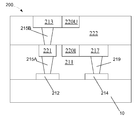
- FIG. 2A (a simplified cross-sectional view) and FIG. 2B (a simplified plan view—without the insulating materials) depict an illustrative semiconductor device 200 at an early stage of manufacturing.
- the device 200 is formed above a semiconducting substrate 10 .
- the substrate 10 may have a variety of configurations, such as the depicted bulk silicon configuration.
- the substrate 10 may also have a silicon-on-insulator (SOI) configuration that includes a bulk silicon layer, a buried insulation layer and an active layer, wherein semiconductor devices are formed in and above the active layer.
- SOI silicon-on-insulator
- the substrate 10 may also be made of materials other than silicon.
- the device 200 is generally comprised of a plurality of schematically depicted constant-power circuits 212 wherein at least some portion of the constant-power circuit 212 requires connection to an uninterruptible power supply structure 220 U, and a plurality of schematically depicted interruptible-power circuits 214 wherein at least some portion or aspect of the circuit 214 are connected to an interruptible power supply structure 220 I.
- the power sources for the uninterruptible power supply structure 220 U and the interruptible power supply structure 220 I are not depicted in the drawings.
- identifying a circuit “constant-power circuit”does not mean that all aspects or functionality of the constant-power circuit 212 needs to be connected to the uninterruptible power supply structure 220 U, although that may be the case in some applications. That is, it may be the case that only portions of a constant-power circuit 212 needs to be connected to the uninterruptible power supply structure 220 U.
- the constant-power circuit 212 and the interruptible power circuit 214 may be part of a single circuit, such as a flip-flop circuit, where portions of the single circuit (i.e., the circuit 214 ) can be connected to the interruptible supply structure 220 I while only the latch (i.e., the circuit 212 ) storing the state of the flip-flop needs to be connected to the uninterruptible power supply structure 220 U.
- identifying a circuit “interruptible-power circuit” does not mean that all aspects or functionality of the interruptible-power circuits 214 can or is connected to the interruptible power supply structure 2201 , although that may be the case in some applications.
- interruptible-power circuits 214 may be connected to the interruptible power supply structure 2201 .
- Illustrative examples of constant-power circuits 212 that may be coupled to the constant power supply structure 220 U include master latches in otherwise interruptible power supply flip-flops, also known as state-retention flip-flops.
- Illustrative examples of interruptible-power circuits 214 that may be coupled to the interruptible power supply 220 I include all remaining circuitry between state retention flip-flops, including the parts of the flip-flops that does not require constant power supply.
- the circuits 212 , 214 are formed in and above the semiconducting substrate 10 .
- the constant-power circuits 212 are conductively coupled to the uninterruptible power supply structure 220 U by schematically depicted conductive vias 215 A, 215 B and conductive lines 221 , 213 .
- the interruptible-power circuits 214 are conductively coupled to the interruptible power supply structure 2201 by a schematically depicted conductive via 219 and a conductive line 217 .
- the various conductive structures 215 A, 221 , 219 , 217 and 2201 are formed in an illustrative layer of insulating material 211
- the various conductive structures 215 B, 213 and 220 U are formed in an illustrative layer of insulating material 222 .
- the various conductive structures 215 A, 221 , 219 , 217 , 2201 , 213 and 220 U may be comprised of a variety of conductive materials, e.g., a metal, and they may be formed using a variety of known techniques.
- the layers of insulating material 211 , 222 may be comprised of a variety of different materials as well, e.g., silicon dioxide, a so-called low-k material (k value less than 3.7), etc.
- the uninterruptible power supply structure 220 U and the interruptible power supply structure 2201 are electrically isolated from one another and, to at least some degree, vertically positioned over one another or vertically stacked. This stacked arrangement of the power supply structures 220 U and 2201 conserves valuable plot space on the device 200 , which is a highly desirable attribute in designing and manufacturing modern integrated circuit devices.
- the uninterruptible power supply structure 220 U is positioned above the interruptible power supply structure 2201 , and they are both the same size and shape.
- the stacking arrangement could be reversed, i.e., the interruptible power supply structure 2201 could be positioned above the uninterruptible power supply structure 220 U, and the size and shape of the power supply structures 220 U, 2201 may be different from one another.
- FIG. 2C depicts the illustrative example wherein the uninterruptible power supply structure 220 U is positioned above the interruptible power supply structure 2201 , but the interruptible power supply structure 2201 is physically wider than the uninterruptible power supply structure 220 U.
- FIG. 2C also depicts an illustrative example wherein the uninterruptible power supply structure 220 U covers less that the entirety of the width of the interruptible power supply structure 2201 .
- FIG. 2D also depicts an illustrative example where the interruptible power supply structure 2201 is positioned above the uninterruptible power supply structure 220 U.
- FIG. 2E depicts one example where there where there is a partial overlap of the two power supply structures, e.g., where the uninterruptible power supply structure 220 U partially overlaps the interruptible power supply structure 2201 by an amount 223 .
- Another unique device disclosed herein includes a device wherein different portions of a single circuit, such as a flip-flop circuit, that have different power-supply requirements may be formed physically adjacent to one another in a semiconducting substrate. Such a device allows for more efficient routing of conductive lines and more efficient use of precious plot space on the semiconducting substrate.
- such a device may include the uninterruptible power supply structure 220 U, the interruptible power supply structure 2201 , and a single circuit that is comprised of a first portion that requires constant power supply and a second portion that does not require constant power supply, wherein the first portion of the single circuit, e.g., the latch, is conductively coupled to the uninterruptible power supply structure 220 U while the second portion of the single circuit is conductively coupled to the interruptible power supply structure 2201 .
- the first portion of the single circuit e.g., the latch
- the various circuits 212 , 214 may be conductively coupled to the power supply structures 220 U, 2201 , respectively, by a variety of known conductive lines and vias that may be formed in multiple layers of insulating material formed above the substrate 10 using a variety of know techniques for forming such conductive structures, e.g., damascene techniques, etc.
- the power supply structures 220 U, 2201 may be formed at any level of the integrated circuit device 200 , i.e., they need not be positioned in immediately adjacent layers of material, although that may be the case in some applications.
Abstract
Description
Claims (22)
Priority Applications (1)
| Application Number | Priority Date | Filing Date | Title |
|---|---|---|---|
| US13/279,687 US9147658B2 (en) | 2011-10-24 | 2011-10-24 | Stacked power supplies for integrated circuit devices and methods of making the same |
Applications Claiming Priority (1)
| Application Number | Priority Date | Filing Date | Title |
|---|---|---|---|
| US13/279,687 US9147658B2 (en) | 2011-10-24 | 2011-10-24 | Stacked power supplies for integrated circuit devices and methods of making the same |
Publications (2)
| Publication Number | Publication Date |
|---|---|
| US20130100590A1 US20130100590A1 (en) | 2013-04-25 |
| US9147658B2 true US9147658B2 (en) | 2015-09-29 |
Family
ID=48135801
Family Applications (1)
| Application Number | Title | Priority Date | Filing Date |
|---|---|---|---|
| US13/279,687 Active 2034-07-30 US9147658B2 (en) | 2011-10-24 | 2011-10-24 | Stacked power supplies for integrated circuit devices and methods of making the same |
Country Status (1)
| Country | Link |
|---|---|
| US (1) | US9147658B2 (en) |
Families Citing this family (1)
| Publication number | Priority date | Publication date | Assignee | Title |
|---|---|---|---|---|
| US10629533B2 (en) | 2018-03-13 | 2020-04-21 | Toshiba Memory Corporation | Power island segmentation for selective bond-out |
Citations (8)
| Publication number | Priority date | Publication date | Assignee | Title |
|---|---|---|---|---|
| US4388534A (en) | 1981-08-11 | 1983-06-14 | Computer Power, Inc. | Uninterruptible power supply |
| US4564767A (en) | 1983-11-07 | 1986-01-14 | Tii Industries, Inc. | Uninterruptible switching power supply system |
| US20030090158A1 (en) | 2001-11-13 | 2003-05-15 | International Business Machines Corporation | System and method for redundant power supply connection |
| US6795322B2 (en) | 1998-12-25 | 2004-09-21 | Hitachi, Ltd. | Power supply with uninterruptible function |
| US6977833B2 (en) * | 2003-10-28 | 2005-12-20 | Lsi Logic Corporation | CMOS isolation cell for embedded memory in power failure environments |
| US20060181857A1 (en) * | 2005-02-16 | 2006-08-17 | Belady Christian L | Redundant power beneath circuit board |
| US20080019203A1 (en) * | 2006-07-19 | 2008-01-24 | Kabushiki Kaisha Toshiba | Semiconductor device |
| US7652333B2 (en) | 2005-12-27 | 2010-01-26 | Renesas Technology Corp. | Semiconductor integrated circuit |
-
2011
- 2011-10-24 US US13/279,687 patent/US9147658B2/en active Active
Patent Citations (11)
| Publication number | Priority date | Publication date | Assignee | Title |
|---|---|---|---|---|
| US4388534A (en) | 1981-08-11 | 1983-06-14 | Computer Power, Inc. | Uninterruptible power supply |
| US4564767A (en) | 1983-11-07 | 1986-01-14 | Tii Industries, Inc. | Uninterruptible switching power supply system |
| US6795322B2 (en) | 1998-12-25 | 2004-09-21 | Hitachi, Ltd. | Power supply with uninterruptible function |
| US7053502B2 (en) | 1998-12-25 | 2006-05-30 | Hitachi, Ltd. | Power supply with uninterruptible function |
| US20030090158A1 (en) | 2001-11-13 | 2003-05-15 | International Business Machines Corporation | System and method for redundant power supply connection |
| US6977833B2 (en) * | 2003-10-28 | 2005-12-20 | Lsi Logic Corporation | CMOS isolation cell for embedded memory in power failure environments |
| US20060181857A1 (en) * | 2005-02-16 | 2006-08-17 | Belady Christian L | Redundant power beneath circuit board |
| US7652333B2 (en) | 2005-12-27 | 2010-01-26 | Renesas Technology Corp. | Semiconductor integrated circuit |
| US20100090282A1 (en) * | 2005-12-27 | 2010-04-15 | Renesas Technology Corp. | Semiconductor integrated circuit |
| US20080019203A1 (en) * | 2006-07-19 | 2008-01-24 | Kabushiki Kaisha Toshiba | Semiconductor device |
| US7843089B2 (en) * | 2006-07-19 | 2010-11-30 | Kabushiki Kaisha Toshiba | Semiconductor device |
Also Published As
| Publication number | Publication date |
|---|---|
| US20130100590A1 (en) | 2013-04-25 |
Similar Documents
| Publication | Publication Date | Title |
|---|---|---|
| US9362486B2 (en) | Magnetic memory device having perpendicular magnetic tunnel junction pattern and method of forming the same | |
| US9881990B2 (en) | Integrated inductor for integrated circuit devices | |
| Jacquet et al. | A 3 GHz dual core processor ARM cortex TM-A9 in 28 nm UTBB FD-SOI CMOS with ultra-wide voltage range and energy efficiency optimization | |
| US11569204B2 (en) | Input output for an integrated circuit | |
| US7312487B2 (en) | Three dimensional integrated circuit | |
| US9461132B2 (en) | Semiconductor device having mid-gap work function metal gate electrode | |
| US9318477B2 (en) | Semiconductor device having dummy cell array | |
| CN108604587B (en) | On-chip integrated passive device | |
| US9252141B2 (en) | Semiconductor integrated circuit, method for fabricating the same, and semiconductor package | |
| US20150179646A1 (en) | Flip-flop layout architecture implementation for semiconductor device | |
| US9754887B2 (en) | Semiconductor devices | |
| JP5581795B2 (en) | STANDARD CELL, SEMICONDUCTOR DEVICE EQUIPPED WITH STANDARD CELL, AND STANDARD CELL PLANNING METHOD | |
| CN102301472A (en) | Techniques for placement of active and passive devices within a chip | |
| US10741536B2 (en) | Magnetic small footprint inductor array module for on-package voltage regulator | |
| US9721898B2 (en) | Methods of forming under device interconnect structures | |
| EP3776652B1 (en) | Massive deep trench capacitor die fill for high performance application specific integrated circuit (asic) applications | |
| US11901274B2 (en) | Packaged integrated circuit device with recess structure | |
| US20170086298A1 (en) | Substrate including structures to couple a capacitor to a packaged device and method of making same | |
| US9147658B2 (en) | Stacked power supplies for integrated circuit devices and methods of making the same | |
| US8466497B2 (en) | Semiconductor integrated circuit chip and layout method for the same | |
| US9305919B2 (en) | Semiconductor devices including cell-type power decoupling capacitors | |
| US20090244948A1 (en) | Embedded memory apparatus with reduced power ring area | |
| CN101211923A (en) | Structure of semiconductor device for decreasing chip area and manufacturing method thereof | |
| US11075206B2 (en) | SRAM source-drain structure | |
| CN109155286B (en) | Heterogeneous cell array |
Legal Events
| Date | Code | Title | Description |
|---|---|---|---|
| AS | Assignment |
Owner name: GLOBALFOUNDRIES INC., CAYMAN ISLANDS Free format text: ASSIGNMENT OF ASSIGNORS INTEREST;ASSIGNOR:DOMAN, DAVID S.;REEL/FRAME:027108/0677 Effective date: 20111012 |
|
| STCF | Information on status: patent grant |
Free format text: PATENTED CASE |
|
| AS | Assignment |
Owner name: WILMINGTON TRUST, NATIONAL ASSOCIATION, DELAWARE Free format text: SECURITY AGREEMENT;ASSIGNOR:GLOBALFOUNDRIES INC.;REEL/FRAME:049490/0001 Effective date: 20181127 |
|
| MAFP | Maintenance fee payment |
Free format text: PAYMENT OF MAINTENANCE FEE, 4TH YEAR, LARGE ENTITY (ORIGINAL EVENT CODE: M1551); ENTITY STATUS OF PATENT OWNER: LARGE ENTITY Year of fee payment: 4 |
|
| AS | Assignment |
Owner name: GLOBALFOUNDRIES U.S. INC., CALIFORNIA Free format text: ASSIGNMENT OF ASSIGNORS INTEREST;ASSIGNOR:GLOBALFOUNDRIES INC.;REEL/FRAME:054633/0001 Effective date: 20201022 |
|
| AS | Assignment |
Owner name: GLOBALFOUNDRIES INC., CAYMAN ISLANDS Free format text: RELEASE BY SECURED PARTY;ASSIGNOR:WILMINGTON TRUST, NATIONAL ASSOCIATION;REEL/FRAME:054636/0001 Effective date: 20201117 |
|
| AS | Assignment |
Owner name: GLOBALFOUNDRIES U.S. INC., NEW YORK Free format text: RELEASE BY SECURED PARTY;ASSIGNOR:WILMINGTON TRUST, NATIONAL ASSOCIATION;REEL/FRAME:056987/0001 Effective date: 20201117 |
|
| MAFP | Maintenance fee payment |
Free format text: PAYMENT OF MAINTENANCE FEE, 8TH YEAR, LARGE ENTITY (ORIGINAL EVENT CODE: M1552); ENTITY STATUS OF PATENT OWNER: LARGE ENTITY Year of fee payment: 8 |