US9136266B2 - Gate oxide quality for complex MOSFET devices - Google Patents
Gate oxide quality for complex MOSFET devices Download PDFInfo
- Publication number
- US9136266B2 US9136266B2 US13/943,229 US201313943229A US9136266B2 US 9136266 B2 US9136266 B2 US 9136266B2 US 201313943229 A US201313943229 A US 201313943229A US 9136266 B2 US9136266 B2 US 9136266B2
- Authority
- US
- United States
- Prior art keywords
- semiconductor device
- material layer
- insulating material
- semiconductor
- silicon
- Prior art date
- Legal status (The legal status is an assumption and is not a legal conclusion. Google has not performed a legal analysis and makes no representation as to the accuracy of the status listed.)
- Expired - Fee Related, expires
Links
Images


Classifications
-
- H—ELECTRICITY
- H10—SEMICONDUCTOR DEVICES; ELECTRIC SOLID-STATE DEVICES NOT OTHERWISE PROVIDED FOR
- H10D—INORGANIC ELECTRIC SEMICONDUCTOR DEVICES
- H10D84/00—Integrated devices formed in or on semiconductor substrates that comprise only semiconducting layers, e.g. on Si wafers or on GaAs-on-Si wafers
- H10D84/80—Integrated devices formed in or on semiconductor substrates that comprise only semiconducting layers, e.g. on Si wafers or on GaAs-on-Si wafers characterised by the integration of at least one component covered by groups H10D12/00 or H10D30/00, e.g. integration of IGFETs
- H10D84/82—Integrated devices formed in or on semiconductor substrates that comprise only semiconducting layers, e.g. on Si wafers or on GaAs-on-Si wafers characterised by the integration of at least one component covered by groups H10D12/00 or H10D30/00, e.g. integration of IGFETs of only field-effect components
- H10D84/83—Integrated devices formed in or on semiconductor substrates that comprise only semiconducting layers, e.g. on Si wafers or on GaAs-on-Si wafers characterised by the integration of at least one component covered by groups H10D12/00 or H10D30/00, e.g. integration of IGFETs of only field-effect components of only insulated-gate FETs [IGFET]
- H10D84/85—Complementary IGFETs, e.g. CMOS
-
- H01L27/092—
-
- H01L29/16—
-
- H01L29/66477—
-
- H01L29/78—
-
- H—ELECTRICITY
- H10—SEMICONDUCTOR DEVICES; ELECTRIC SOLID-STATE DEVICES NOT OTHERWISE PROVIDED FOR
- H10D—INORGANIC ELECTRIC SEMICONDUCTOR DEVICES
- H10D30/00—Field-effect transistors [FET]
- H10D30/01—Manufacture or treatment
- H10D30/021—Manufacture or treatment of FETs having insulated gates [IGFET]
- H10D30/027—Manufacture or treatment of FETs having insulated gates [IGFET] of lateral single-gate IGFETs
- H10D30/0278—Manufacture or treatment of FETs having insulated gates [IGFET] of lateral single-gate IGFETs forming single crystalline channels on wafers after forming insulating device isolations
-
- H—ELECTRICITY
- H10—SEMICONDUCTOR DEVICES; ELECTRIC SOLID-STATE DEVICES NOT OTHERWISE PROVIDED FOR
- H10D—INORGANIC ELECTRIC SEMICONDUCTOR DEVICES
- H10D30/00—Field-effect transistors [FET]
- H10D30/60—Insulated-gate field-effect transistors [IGFET]
-
- H—ELECTRICITY
- H10—SEMICONDUCTOR DEVICES; ELECTRIC SOLID-STATE DEVICES NOT OTHERWISE PROVIDED FOR
- H10D—INORGANIC ELECTRIC SEMICONDUCTOR DEVICES
- H10D30/00—Field-effect transistors [FET]
- H10D30/60—Insulated-gate field-effect transistors [IGFET]
- H10D30/751—Insulated-gate field-effect transistors [IGFET] having composition variations in the channel regions
-
- H—ELECTRICITY
- H10—SEMICONDUCTOR DEVICES; ELECTRIC SOLID-STATE DEVICES NOT OTHERWISE PROVIDED FOR
- H10D—INORGANIC ELECTRIC SEMICONDUCTOR DEVICES
- H10D62/00—Semiconductor bodies, or regions thereof, of devices having potential barriers
- H10D62/80—Semiconductor bodies, or regions thereof, of devices having potential barriers characterised by the materials
- H10D62/83—Semiconductor bodies, or regions thereof, of devices having potential barriers characterised by the materials being Group IV materials, e.g. B-doped Si or undoped Ge
-
- H10D64/0134—
-
- H10D64/01342—
-
- H10D64/01344—
-
- H10D64/01352—
-
- H—ELECTRICITY
- H10—SEMICONDUCTOR DEVICES; ELECTRIC SOLID-STATE DEVICES NOT OTHERWISE PROVIDED FOR
- H10D—INORGANIC ELECTRIC SEMICONDUCTOR DEVICES
- H10D84/00—Integrated devices formed in or on semiconductor substrates that comprise only semiconducting layers, e.g. on Si wafers or on GaAs-on-Si wafers
- H10D84/01—Manufacture or treatment
- H10D84/0123—Integrating together multiple components covered by H10D12/00 or H10D30/00, e.g. integrating multiple IGBTs
- H10D84/0126—Integrating together multiple components covered by H10D12/00 or H10D30/00, e.g. integrating multiple IGBTs the components including insulated gates, e.g. IGFETs
- H10D84/0128—Manufacturing their channels
-
- H—ELECTRICITY
- H10—SEMICONDUCTOR DEVICES; ELECTRIC SOLID-STATE DEVICES NOT OTHERWISE PROVIDED FOR
- H10D—INORGANIC ELECTRIC SEMICONDUCTOR DEVICES
- H10D84/00—Integrated devices formed in or on semiconductor substrates that comprise only semiconducting layers, e.g. on Si wafers or on GaAs-on-Si wafers
- H10D84/01—Manufacture or treatment
- H10D84/0123—Integrating together multiple components covered by H10D12/00 or H10D30/00, e.g. integrating multiple IGBTs
- H10D84/0126—Integrating together multiple components covered by H10D12/00 or H10D30/00, e.g. integrating multiple IGBTs the components including insulated gates, e.g. IGFETs
- H10D84/0144—Manufacturing their gate insulating layers
-
- H—ELECTRICITY
- H10—SEMICONDUCTOR DEVICES; ELECTRIC SOLID-STATE DEVICES NOT OTHERWISE PROVIDED FOR
- H10D—INORGANIC ELECTRIC SEMICONDUCTOR DEVICES
- H10D84/00—Integrated devices formed in or on semiconductor substrates that comprise only semiconducting layers, e.g. on Si wafers or on GaAs-on-Si wafers
- H10D84/01—Manufacture or treatment
- H10D84/02—Manufacture or treatment characterised by using material-based technologies
- H10D84/03—Manufacture or treatment characterised by using material-based technologies using Group IV technology, e.g. silicon technology or silicon-carbide [SiC] technology
- H10D84/038—Manufacture or treatment characterised by using material-based technologies using Group IV technology, e.g. silicon technology or silicon-carbide [SiC] technology using silicon technology, e.g. SiGe
-
- H—ELECTRICITY
- H10—SEMICONDUCTOR DEVICES; ELECTRIC SOLID-STATE DEVICES NOT OTHERWISE PROVIDED FOR
- H10D—INORGANIC ELECTRIC SEMICONDUCTOR DEVICES
- H10D84/00—Integrated devices formed in or on semiconductor substrates that comprise only semiconducting layers, e.g. on Si wafers or on GaAs-on-Si wafers
- H10D84/80—Integrated devices formed in or on semiconductor substrates that comprise only semiconducting layers, e.g. on Si wafers or on GaAs-on-Si wafers characterised by the integration of at least one component covered by groups H10D12/00 or H10D30/00, e.g. integration of IGFETs
- H10D84/82—Integrated devices formed in or on semiconductor substrates that comprise only semiconducting layers, e.g. on Si wafers or on GaAs-on-Si wafers characterised by the integration of at least one component covered by groups H10D12/00 or H10D30/00, e.g. integration of IGFETs of only field-effect components
- H10D84/83—Integrated devices formed in or on semiconductor substrates that comprise only semiconducting layers, e.g. on Si wafers or on GaAs-on-Si wafers characterised by the integration of at least one component covered by groups H10D12/00 or H10D30/00, e.g. integration of IGFETs of only field-effect components of only insulated-gate FETs [IGFET]
-
- H—ELECTRICITY
- H10—SEMICONDUCTOR DEVICES; ELECTRIC SOLID-STATE DEVICES NOT OTHERWISE PROVIDED FOR
- H10D—INORGANIC ELECTRIC SEMICONDUCTOR DEVICES
- H10D62/00—Semiconductor bodies, or regions thereof, of devices having potential barriers
- H10D62/80—Semiconductor bodies, or regions thereof, of devices having potential barriers characterised by the materials
- H10D62/82—Heterojunctions
- H10D62/822—Heterojunctions comprising only Group IV materials heterojunctions, e.g. Si/Ge heterojunctions
-
- H—ELECTRICITY
- H10—SEMICONDUCTOR DEVICES; ELECTRIC SOLID-STATE DEVICES NOT OTHERWISE PROVIDED FOR
- H10D—INORGANIC ELECTRIC SEMICONDUCTOR DEVICES
- H10D64/00—Electrodes of devices having potential barriers
- H10D64/60—Electrodes characterised by their materials
- H10D64/66—Electrodes having a conductor capacitively coupled to a semiconductor by an insulator, e.g. MIS electrodes
- H10D64/68—Electrodes having a conductor capacitively coupled to a semiconductor by an insulator, e.g. MIS electrodes characterised by the insulator, e.g. by the gate insulator
- H10D64/681—Electrodes having a conductor capacitively coupled to a semiconductor by an insulator, e.g. MIS electrodes characterised by the insulator, e.g. by the gate insulator having a compositional variation, e.g. multilayered
- H10D64/685—Electrodes having a conductor capacitively coupled to a semiconductor by an insulator, e.g. MIS electrodes characterised by the insulator, e.g. by the gate insulator having a compositional variation, e.g. multilayered being perpendicular to the channel plane
Definitions
- the present invention generally relates to improving the quality of gate oxides in complex MOSFET devices, and, more particularly, to the formation of conductive channel regions below gate electrodes of complex MOSFET devices.
- present-day integrated circuits are implemented by using a plurality of interconnected field effect transistors (FETs), also called metal oxide semiconductor field effect transistors (MOSFETs) or simply MOS transistors.
- FETs field effect transistors
- MOSFETs metal oxide semiconductor field effect transistors
- present-day integrated circuits are implemented by millions of MOS transistors which are formed on a semiconductor substrate with a given surface area.
- MOS transistors act as electronic switching elements, wherein a current through a channel region formed between source and drain regions of a MOS transistor is controlled by a gate electrode which is typically disposed over the channel region, independent of whether a PMOS transistor or an NMOS transistor is considered.
- a gate electrode which is typically disposed over the channel region, independent of whether a PMOS transistor or an NMOS transistor is considered.
- the conductivity state of a transistor is changed by a voltage applied to the gate electrode passing a so-called threshold voltage (Vt).
- Vt threshold voltage
- the threshold voltage depends nontrivially on the transistor's properties, such as size, material, etc.
- a severe issue met by developers when attempting to exceed current technology nodes is given by constraints on maximum thicknesses of gate dielectrics in advanced gate electrodes set by the requirement of implementing a sufficiently high capacitive coupling between the gate electrode and the underlying channel region so as to reliably control a conductivity state of the channel region, while suppressing leakage currents of the gate electrode into the channel region through the gate dielectric.
- this becomes an increasingly critical issue because the capacitive coupling of the gate electrode to the channel region strongly depends on the thickness of the gate dielectric.
- a gate dielectric with a sufficiently small thickness has to be provided.
- the probability of tunneling of charge-carriers through the gate dielectric and, therefore, the presence of a tunneling current between gate electrode and channel region increases with decreasing thickness of the gate dielectric.
- This situation has been addressed by using so-called high-k dielectrics having k-values greater than 5 which allow, on the one hand, increasing the thickness of the gate dielectric so as to reduce the tunneling currents, while, on the other hand, maintaining a sufficiently high capacitive coupling between the gate electrode and the channel region due to its high electrical permeability.
- a large number of different semiconductor devices and device structures are formed in order to implement a plurality of required functions on a microchip.
- current integrated circuits may comprise a huge number (on the order of millions) of EG devices and SG devices which are disposed at different device areas of the semiconductor substrate on which the integrated circuit is to be formed on. Due to current high integration densities of complex semiconductor devices at present reaching the deep submicron regime, it is not hard to see that fabrication methods are highly complex and involve a large number of different processes to form individual semiconductor devices and semiconductor device structures on a given surface of a semiconductor wafer in accordance with a desired layout. In current fabrication processes, processing time may be reduced by performing a multitude of different semiconductor devices in parallel when possible, which also helps to save manufacturing costs.
- EG devices have a much thicker gate oxide when compared to SG devices because EG devices are usually used as input-output devices (I/O devices) at peripheral regions of integrated circuits where usually comparably high voltages are applied (possibly up to about 15 V).
- I/O devices input-output devices
- the risk of gate dielectric breakdown, i.e., a breakthrough of gate oxide, is reduced with increasing gate oxide thickness, due to gate electrodes with thicker gate oxides supporting higher gate voltages. Consequently, device failure is prevented.
- EG devices and SG devices are fabricated in parallel, wherein a thick gate oxide layer is formed over EG and SG device regions, followed by an etching process for etching of the thick gate oxide from above the SG device regions. Subsequently, gate oxides are formed over the SG device regions and a gate etch is performed to pattern gate electrodes in EG device regions and SG device regions.
- the thick gate oxides for EG devices are conventionally created by high temperature oxidation (HTO) processes which show faster oxide growth rates as compared to low temperature oxidation processes, such as oxide deposition by chemical vapor deposition (CVD) at about 600° C., for instance, used in TEOS processes.
- HTO high temperature oxidation
- CVD chemical vapor deposition
- Conventional high temperature oxidation processes are performed as low pressure chemical vapor deposition (LPCVD) deposition processes at temperatures of about 900° C. using a combination of dichlorosilane SiH 2 CL 2 and N 2 O.
- a silicon/germanium layer is provided on a semiconductor substrate.
- at least one insulating material layer is formed on the silicon/germanium layer.
- the at least one insulating material layer is removed in subsequent process sequences such that the silicon/germanium layer is at least partially exposed.
- a gate electrode is formed on the exposed silicon/germanium layer.
- a method of forming a semiconductor device includes forming a silicon/germanium layer on a surface of a semiconductor substrate, forming at least one insulating material layer on the silicon/germanium layer, thereafter performing an annealing process, removing the at least one insulating material layer for exposing a surface of the silicon/germanium layer, and forming a gate dielectric material layer on the exposed surface of the silicon/germanium layer.
- a method of forming a semiconductor device structure includes providing a semiconductor substrate with a first semiconductor device region and a second semiconductor device region, forming a silicon/germanium layer on the semiconductor substrate in the first semiconductor device region, forming at least one insulating material layer over the semiconductor substrate in the first and second semiconductor device regions, thereafter performing an annealing process, removing the at least one insulating material layer in the first semiconductor device region for exposing a surface of the silicon/germanium layer, and forming a gate dielectric material layer on the exposed surface of the silicon/germanium layer.
- the semiconductor device includes a silicon/germanium channel formed on a surface of a semiconductor substrate and a gate dielectric layer formed on the silicon/germanium channel. Furthermore, the semiconductor device has a DIT of substantially smaller than 5.3E11.
- the semiconductor device structure includes a first semiconductor device formed in a first semiconductor device region of a semiconductor substrate and a second semiconductor device formed in a second semiconductor device region of the semiconductor substrate.
- the first semiconductor device includes a silicon/germanium channel formed on a surface of a semiconductor substrate and a gate dielectric layer formed on the silicon/germanium channel.
- the second semiconductor device includes at least one insulating material layer formed on the surface of the semiconductor substrate.
- the first semiconductor device has a DIT of less than 5.3E11.
- FIGS. 1-6 schematically illustrate in cross-sectional views illustrative process flows of fabricating semiconductor devices in accordance with illustrative embodiments of the present disclosure
- FIG. 7 schematically illustrates an interface trap density of conventional semiconductor device structures in comparison with semiconductor device structures of illustrative embodiments of the present disclosure.
- FIGS. 8 a - 8 b schematically illustrate graphical relations between the mobility of charge carriers and gate lengths of conventional NMOS and PMOS devices in comparison with NMOS and PMOS devices of illustrative embodiments of the present disclosure.
- the present invention relates to semiconductor device structures and particularly to semiconductor devices such as metal oxide semiconductor devices or MOS devices.
- MOS device any limitation to a metal-containing gate material and/or to an oxide-containing gate dielectric material is intended.
- Semiconductor devices of the present disclosure and particularly MOS devices as illustrated by means of some illustrative embodiments as described herein concern devices fabricated by using advanced technologies.
- Semiconductor devices and particularly MOS devices of the present disclosure are fabricated by technologies applied to approach technology nodes smaller than 100 nm, preferably smaller than 50 nm, more preferably smaller than 35 nm.
- the present disclosure suggests semiconductor devices, and particularly MOS devices, having gate structures such as gate stacks having a gate electrode material layer and a gate dielectric material layer with a length dimension smaller than 100 nm, preferably smaller than 50 nm, more preferably smaller than 35 nm.
- the present invention suggests providing methods of achieving reliable encapsulation of gate structures at very early stages of fabrication.
- MOS transistors may be fabricated as P-channel MOS transistors or PMOS transistors and as N-channel transistors or NMOS transistors, and both may be fabricated with or without mobility enhancing stressor features or strain-inducing features.
- a circuit designer can mix and match device types, using PMOS and NMOS transistors, stressed and unstressed, to take advantage of the best characteristics of each device type as they best suit the circuit being designed.
- stress and strain may be generally described with regard to the tensile modulus.
- semiconductor device structures and methods of forming a semiconductor device in accordance with various exemplary embodiments of the present disclosure will be illustrated.
- the described process steps, procedures and materials are to be considered only as exemplary embodiments designed to illustrate to one of ordinary skill in the art methods for practicing the invention.
- the invention is not exclusively limited to the illustrated and described exemplary embodiments as many possible modifications and changes exist which will become clear to the ordinary skilled in the art when studying the present detailed description together with the accompanied drawings and the above background and summary of the invention.
- Illustrated portions of semiconductor devices and semiconductor device structures may include only a single MOS structure, although those skilled in the art will recognize that actual implementations of integrated circuits may include a large number of such structures.
- Various steps in the manufacture of semiconductor devices and semiconductor device structures are well known and so, in the interest of brevity, many conventional steps will only be mentioned briefly herein, or will be omitted entirely without providing the well-known process details.
- FIGS. 1-6 various illustrative embodiments of the present invention will be described in greater detail.
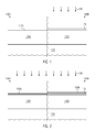
- FIG. 1 shows a semiconductor device structure at an early stage during fabrication, wherein the semiconductor device structure comprises semiconductor device regions 100 A and 100 B.
- the semiconductor device region 100 A comprises a semiconductor material layer 115 A
- the semiconductor device region 100 B comprises a semiconductor material layer 115 B.
- the semiconductor device regions 100 A and 100 B, and accordingly the semiconductor material layers 115 A and 115 B may be directly adjacent to each other or may be separated by one or more further semiconductor device regions (not illustrated) which may be formed in between the semiconductor device regions 100 A and 100 B. It is further possible that the semiconductor device regions 100 A and 100 B are delineated and/or separated by one or more further insulating regions (not illustrated), such as shallow trench isolations (STI) or the like.
- STI shallow trench isolations
- the semiconductor material layers 115 A and 115 B may be composed of the same material or may have different material compositions.
- the semiconductor material layers 115 A, 115 B may be composed of silicon, silicon/germanium, silicon carbide, and combinations thereof.
- the semiconductor material layers 115 A, 115 B may have dopants incorporated therein for forming at least one of a P-well and an N-well.
- the semiconductor material layers 115 A, 115 B may be formed on a further material 110 , which may be given by a semiconductor substrate, such as a silicon substrate as conventionally used in bulk configurations, or may represent an insulating material such as conventionally used on silicon-on-insulator (SOI) configurations.
- SOI silicon-on-insulator
- the material 110 may in special illustrative examples be explicitly given by a buried oxide (BOX) layer.
- BOX buried oxide
- a silicon/germanium layer 125 is formed on a surface 115 S of the semiconductor material layer in the semiconductor device region 100 B, particularly on the surface 115 S of the semiconductor material layer 115 B.
- the semiconductor device region 100 A is not exposed to the deposition process 120 and particularly no material is deposited on the surface 115 S of the semiconductor material layer 115 A in the semiconductor device region 100 A.
- a masking pattern (not illustrated) may be formed over the semiconductor material layer 115 A such that the semiconductor device region 100 B is exposed to the deposition process 120 , while the semiconductor device region 100 A is prevented from being exposed to the deposition process 120 .
- the deposition process 120 may be a molecular beam epitaxy (MBE) process in which a germanium content of about 20-45% may be incorporated into silicon such that a silicon/germanium layer having a germanium content of about 20-45% may be epitaxially grown.
- MBE molecular beam epitaxy
- FIG. 2 illustrates the semiconductor device regions 100 A, 100 B at a more advanced stage during fabrication, particularly when a further deposition process 130 is applied to the semiconductor device regions 100 A, 100 B.
- the further deposition process 130 is performed to deposit an insulating material, such as a silicon oxide material, on the surface 115 S (see FIG. 1 ) of the semiconductor material layer 115 A in the semiconductor device region 100 A.
- an insulating material layer 130 A is formed on the surface 115 S of the semiconductor material layer 115 A in the semiconductor device region 100 A and an insulating material layer 130 B is formed on the silicon/germanium layer 125 in the semiconductor device region 100 B.
- the insulating material layer 130 B is formed over the semiconductor material layer 115 B and disposed on the silicon/germanium layer 125 .
- the person skilled in the art will appreciate that the insulating material layer 130 B may protect the silicon/germanium layer 125 in the semiconductor device region 100 B from deteriorating effects of subsequently performed process sequences. For example, as silicon/germanium materials have different etching rates when compared to silicon, for instance, undue loss of silicon/germanium material may appear in cleaning and etching process sequences to which silicon/germanium materials may be exposed.
- the insulating material layers 130 A, 130 B may be formed with a thickness of 10 nm or less, or 5 nm or less.
- the insulating material layers 130 A, 130 B may comprise a silicon oxide material, a silicon nitride material or the like. However, this does not pose any limitation to the present disclosure and the person skilled in the art will appreciate that, in some alternative embodiments, the insulating material layers 130 A, 130 B may be omitted.
- FIG. 3 illustrates the semiconductor device regions 100 A, 100 B at a more advanced stage during fabrication, particularly when another deposition process 140 is performed to deposit a second insulating material over the semiconductor material layers 115 A, 115 B.
- a second insulating material layer 140 A is formed over the semiconductor material layer 115 A and particularly on the insulating material layer 130 A.
- a second insulating material layer 140 B is formed over the semiconductor material layer 115 B and particularly on the insulating material layer 130 B.
- the deposition process 140 may comprise an LPCVD process performed at temperatures greater than 800° C.
- a combination of dichlorosilane SiH 2 Cl 2 and N 2 O may be used at temperatures of 900° C. or more in order to form a high thermal oxide (HTO) layer of SiO 2 material on the insulating material layers 130 B, 130 A.
- HTO high thermal oxide
- FIG. 4 shows the semiconductor device structure at a more advanced stage during fabrication when an annealing process 150 is applied to the semiconductor device structure.
- the annealing process 150 may comprise an annealing sequence at an annealing temperature higher than 800° C.
- the annealing temperature may be in a range from about 850-1000° C., such as, for example, about 900° C.
- the illustrative annealing sequence may be performed in an inert atmosphere, for example a nitrogen atmosphere implementing an N2 annealing process.
- an argon atmosphere may be used instead of the nitrogen atmosphere.
- FIG. 5 shows the semiconductor device structure at a more advanced stage during fabrication, at which a removal process 160 is applied to the semiconductor device region 100 B so as to remove the insulating material layers 140 B and 130 B from above the silicon/germanium layer 125 .
- etch chemistry may be used: 50A POU-DHF; SPM; 120S cold APM with about 100% MEGASONIC rinse; HPM.
- etch chemistry may be used: 50A POU-DHF; SPM; 120S cold APM with about 100% MEGASONIC rinse; HPM.
- the silicon layer may be formed on the silicon/germanium layer such that the silicon/germanium layer is protected from undue loss of silicon/germanium material and surface roughness.
- the semiconductor device region 100 A is not exposed to the removal process 160 . This may be achieved by forming an appropriate masking pattern over the semiconductor device region 100 A for protecting the second insulating material 140 A in the semiconductor device region 100 A.
- the removal process 160 is completed.
- the surface 125 S is still attacked by the removal process 160 , resulting in an increased surface roughness for the silicon/germanium material layer 125 .
- the present disclosure may result in a surface roughness of the surface 125 S that is improved in comparison with the state of the art.
- FIG. 6 shows the semiconductor device structure at a more advanced stage during fabrication, at which a further deposition process 170 is applied to the semiconductor region 100 B so as to form a gate dielectric material layer 175 on the silicon/germanium material layer 125 in the semiconductor device region 100 B.
- the person skilled in the art will appreciate that the deposition process 170 may be implemented such that the gate dielectric material layer 175 is formed for providing a desired semiconductor device in the semiconductor device region 100 B.
- the gate dielectric material layer may comprise one or more sub-layers (not illustrated) comprising at least at least one of high-k dielectric materials and work function adjusting materials.
- the semiconductor device region 100 A is not exposed to the deposition process 170 , for instance, by having a masking pattern (not illustrated) formed over the second insulating material layer 140 A.
- processing may continue by forming gate electrode material layers over the semiconductor device regions 100 A and 100 B and applying patterning sequences (not illustrated) to form gate electrode structures (not illustrated) in the semiconductor device regions 100 A and 100 B. Therefore, one or more gate electrode structures (not illustrated) may be formed within the semiconductor device region 100 A, the one or more gate electrode structures (not illustrated) having thick gate dielectric layers ( 130 A, 140 A in FIG. 6 ), while one or more gate electrode structures (not illustrated) formed in the semiconductor device region 100 B have comparably thin gate dielectric layers ( 125 , 175 in FIG. 6 ).
- gate electrode structures (not illustrated) formed in semiconductor device regions 100 A may be advantageously used as I/O semiconductor devices to which high voltages, such as 5V or more, or 10V or more, may be applied during operation.
- high voltages such as 5V or more, or 10V or more
- semiconductor devices provided in the semiconductor device region 100 A may be I/O devices having much thicker gate oxides such that higher voltages may be applied, e.g., EG devices, while semiconductor devices provided in the semiconductor device region 100 B may be normal core devices, e.g., SG devices.
- FIG. 7 schematically illustrates interface trap densities (DIT) measured by charge pumping for semiconductor devices of the present disclosure and conventional semiconductor devices.
- charge pumping is a well-known technique for characterizing semiconductor/dielectric interfaces of semiconductor device structures. Invaluable information about the quality and degradation of a device may be obtained from charge-pumping-current measurements, including information about the interface-trap density and the mean-capture cross section. For example, charge-pumping-current measurements may be performed by pulsing a gate voltage and measuring a DC substrate current simultaneously.
- a gate of a transistor to be measured is connected with a pulse generator, which is configured to repeatedly switch the transistor from accumulation to inversion.
- a recombination process of majority and minority carriers occurs on the rising and falling edges of the pulses, causing a current to flow in the opposite direction of the normal drain-to-source current.
- This induced current may be measured by connecting a sensitive ammeter to the substrate, or bulk terminal, of the transistor.
- the substrate current is usually measured while voltage pulses of known amplitude, rise time and frequency are applied to the transistor gate.
- Source and drain may be either connected to a ground potential or may be slightly reverse-biased.
- charge-pumping techniques such as using different amplitudes (fixed, variable voltage amplitude being pulsed into inversion, etc.), voltage waveform shapes, varying rise and fall times, measuring the charge-pumping current as a function of frequency.
- FIG. 7 illustrates box-plots obtained in measurements applied to conventional semiconductor devices presented by the box-plot at the left (denoted by “P”) in comparison with measurements applied to semiconductor devices in accordance with the present disclosure as presented by the box-plot on the right hand (denoted by “J”).
- FIG. 8 a shows a graphic relation between mobility of charge carriers ( ⁇ measured in Cm 2 /Vs, ordinate) and gate length (L measured in nanometer abscissa) for NMOS devices of the present disclosure having a width of 1 ⁇ m, wherein the gate length value plotted on the abscissa presents median values.
- Solid lines denoted by reference number G 1 relate to NMOS devices exposed to a high thermal anneal (annealing process 150 in FIG. 4 ).
- Broken lines denoted by reference numeral G 2 relate to conventional semiconductor devices used as comparison samples.
- FIG. 8 a shows that the mobility of NMOS devices is improved to a small extent as the broken line G 2 is only slightly underneath the solid line G 1 .
- FIG. 8 b shows another graphic relation between mobility of charge carriers ( ⁇ measured in Cm 2 /Vs, ordinate) and gate length (L measured in nanometer abscissa) in the case of PMOS devices of the present disclosure having a width of 1 ⁇ m, wherein the gate length value plotted on the abscissa presents median values.
- Solid lines denoted by reference number G 3 relate to NMOS devices exposed to a high thermal anneal (annealing process 150 in FIG. 4 ).
- Broken lines denoted by reference numerals G 4 and G 5 relate to conventional semiconductor devices used as comparison samples.
- PMOS devices subjected to the additional high annealing process show a considerably improved mobility which is even maintained down to small length scales.
- the mobility ⁇ of PMOS semiconductor devices according to the present disclosure is improved by at least 55% as opposed to conventional semiconductor devices used as comparison samples for a given gate length.
- semiconductor device structures of the present disclosure show a reduced variation due to interface charge trapping and deep trapping effects at interfaces between semiconductor material layer and gate dielectric material layer. Consequently, the reliability of semiconductor devices is improved by the methods and devices presented in the present disclosure.
- first insulating material layer and a second insulating material layer This does not pose any limitation to the present disclosure.
- the person skilled in the art will appreciate that, in alternative illustrative embodiments, one of the first insulating material layer and the second insulating material layer may be omitted and instead only one insulating material layer may be provided. Therefore, one of the deposition process 120 in FIG. 1 and the process 130 in FIG. 2 may be optional and, consequently, may be omitted in alternative embodiments.
- more than two insulating material layers may be formed prior to the anneal.
- the annealing process 150 performed in FIG. 4 helps to reduce silicon/germanium loss to which conventional semiconductor devices are subjected when removing the insulating material layer from above the silicon/germanium channel. Therefore, the present disclosure allows improvement of electrical properties of gate dielectric material layers, which are critical to the formation of a conductive channel region below a gate electrode.
Landscapes
- Insulated Gate Type Field-Effect Transistor (AREA)
Abstract
Description
Claims (14)
Priority Applications (1)
| Application Number | Priority Date | Filing Date | Title |
|---|---|---|---|
| US13/943,229 US9136266B2 (en) | 2013-07-16 | 2013-07-16 | Gate oxide quality for complex MOSFET devices |
Applications Claiming Priority (1)
| Application Number | Priority Date | Filing Date | Title |
|---|---|---|---|
| US13/943,229 US9136266B2 (en) | 2013-07-16 | 2013-07-16 | Gate oxide quality for complex MOSFET devices |
Publications (2)
| Publication Number | Publication Date |
|---|---|
| US20150021703A1 US20150021703A1 (en) | 2015-01-22 |
| US9136266B2 true US9136266B2 (en) | 2015-09-15 |
Family
ID=52342900
Family Applications (1)
| Application Number | Title | Priority Date | Filing Date |
|---|---|---|---|
| US13/943,229 Expired - Fee Related US9136266B2 (en) | 2013-07-16 | 2013-07-16 | Gate oxide quality for complex MOSFET devices |
Country Status (1)
| Country | Link |
|---|---|
| US (1) | US9136266B2 (en) |
Cited By (1)
| Publication number | Priority date | Publication date | Assignee | Title |
|---|---|---|---|---|
| US11387338B1 (en) | 2021-01-22 | 2022-07-12 | Applied Materials, Inc. | Methods for forming planar metal-oxide-semiconductor field-effect transistors |
Families Citing this family (1)
| Publication number | Priority date | Publication date | Assignee | Title |
|---|---|---|---|---|
| US10872898B2 (en) * | 2017-07-19 | 2020-12-22 | Cypress Semiconductor Corporation | Embedded non-volatile memory device and fabrication method of the same |
Citations (1)
| Publication number | Priority date | Publication date | Assignee | Title |
|---|---|---|---|---|
| US20100167482A1 (en) * | 2008-12-26 | 2010-07-01 | Shinji Mori | Semiconductor device manufacturing method |
-
2013
- 2013-07-16 US US13/943,229 patent/US9136266B2/en not_active Expired - Fee Related
Patent Citations (1)
| Publication number | Priority date | Publication date | Assignee | Title |
|---|---|---|---|---|
| US20100167482A1 (en) * | 2008-12-26 | 2010-07-01 | Shinji Mori | Semiconductor device manufacturing method |
Cited By (1)
| Publication number | Priority date | Publication date | Assignee | Title |
|---|---|---|---|---|
| US11387338B1 (en) | 2021-01-22 | 2022-07-12 | Applied Materials, Inc. | Methods for forming planar metal-oxide-semiconductor field-effect transistors |
Also Published As
| Publication number | Publication date |
|---|---|
| US20150021703A1 (en) | 2015-01-22 |
Similar Documents
| Publication | Publication Date | Title |
|---|---|---|
| US8476131B2 (en) | Methods of forming a semiconductor device with recessed source/design regions, and a semiconductor device comprising same | |
| US9472642B2 (en) | Method of forming a semiconductor device structure and such a semiconductor device structure | |
| US20150076610A1 (en) | Field Effect Transistor Structure Having One or More Fins | |
| US8278164B2 (en) | Semiconductor structures and methods of manufacturing the same | |
| US7977178B2 (en) | Asymmetric source/drain junctions for low power silicon on insulator devices | |
| KR20090038653A (en) | CMOS device and method of manufacturing the same | |
| US10319732B2 (en) | Transistor element including a buried insulating layer having enhanced functionality | |
| US20170194425A1 (en) | Semiconductor devices including field effect transistors | |
| US9876111B2 (en) | Method of forming a semiconductor device structure using differing spacer widths and the resulting semiconductor device structure | |
| US11404539B2 (en) | Apparatus for extension of operation voltage | |
| US9460957B2 (en) | Method and structure for nitrogen-doped shallow-trench isolation dielectric | |
| US9136266B2 (en) | Gate oxide quality for complex MOSFET devices | |
| US8581340B2 (en) | Semiconductor device of which breakdown voltage is improved | |
| US9953876B1 (en) | Method of forming a semiconductor device structure and semiconductor device structure | |
| US20060079046A1 (en) | Method and structure for improving cmos device reliability using combinations of insulating materials | |
| CN108039362B (en) | Transistor, clamping circuit and integrated circuit | |
| US11437372B2 (en) | Liner structures | |
| CN108039365A (en) | Transistor, clamping circuit and integrated circuit | |
| US20150102410A1 (en) | Semiconductor device including stress layer adjacent channel and related methods | |
| US20140353733A1 (en) | Protection of the gate stack encapsulation | |
| US20120126334A1 (en) | Breakdown voltage improvement with a floating substrate | |
| US8853051B2 (en) | Methods of recessing an active region and STI structures in a common etch process | |
| US20250294869A1 (en) | Novel liner structures | |
| Mori et al. | A novel divided STI-based nLDMOSFET for suppressing HCI degradation under high gate bias stress | |
| US8405156B2 (en) | Semiconductor device and manufacturing method thereof |
Legal Events
| Date | Code | Title | Description |
|---|---|---|---|
| AS | Assignment |
Owner name: GLOBALFOUNDRIES INC., CAYMAN ISLANDS Free format text: ASSIGNMENT OF ASSIGNORS INTEREST;ASSIGNORS:YAN, RAN;SASSIAT, NICOLAS;HOENTSCHEL, JAN;AND OTHERS;SIGNING DATES FROM 20130610 TO 20130617;REEL/FRAME:030807/0060 |
|
| STCF | Information on status: patent grant |
Free format text: PATENTED CASE |
|
| CC | Certificate of correction | ||
| AS | Assignment |
Owner name: WILMINGTON TRUST, NATIONAL ASSOCIATION, DELAWARE Free format text: SECURITY AGREEMENT;ASSIGNOR:GLOBALFOUNDRIES INC.;REEL/FRAME:049490/0001 Effective date: 20181127 |
|
| FEPP | Fee payment procedure |
Free format text: MAINTENANCE FEE REMINDER MAILED (ORIGINAL EVENT CODE: REM.); ENTITY STATUS OF PATENT OWNER: LARGE ENTITY |
|
| LAPS | Lapse for failure to pay maintenance fees |
Free format text: PATENT EXPIRED FOR FAILURE TO PAY MAINTENANCE FEES (ORIGINAL EVENT CODE: EXP.); ENTITY STATUS OF PATENT OWNER: LARGE ENTITY |
|
| STCH | Information on status: patent discontinuation |
Free format text: PATENT EXPIRED DUE TO NONPAYMENT OF MAINTENANCE FEES UNDER 37 CFR 1.362 |
|
| FP | Lapsed due to failure to pay maintenance fee |
Effective date: 20190915 |
|
| AS | Assignment |
Owner name: GLOBALFOUNDRIES INC., CAYMAN ISLANDS Free format text: RELEASE BY SECURED PARTY;ASSIGNOR:WILMINGTON TRUST, NATIONAL ASSOCIATION;REEL/FRAME:054636/0001 Effective date: 20201117 |
|
| AS | Assignment |
Owner name: GLOBALFOUNDRIES U.S. INC., NEW YORK Free format text: RELEASE BY SECURED PARTY;ASSIGNOR:WILMINGTON TRUST, NATIONAL ASSOCIATION;REEL/FRAME:056987/0001 Effective date: 20201117 Owner name: GLOBALFOUNDRIES U.S. INC., NEW YORK Free format text: RELEASE OF SECURITY INTEREST;ASSIGNOR:WILMINGTON TRUST, NATIONAL ASSOCIATION;REEL/FRAME:056987/0001 Effective date: 20201117 |