US9129798B1 - Methods of forming semiconductor structures comprising aluminum oxide - Google Patents
Methods of forming semiconductor structures comprising aluminum oxide Download PDFInfo
- Publication number
- US9129798B1 US9129798B1 US14/184,452 US201414184452A US9129798B1 US 9129798 B1 US9129798 B1 US 9129798B1 US 201414184452 A US201414184452 A US 201414184452A US 9129798 B1 US9129798 B1 US 9129798B1
- Authority
- US
- United States
- Prior art keywords
- aluminum
- metal
- aluminum oxide
- titanium
- forming
- Prior art date
- Legal status (The legal status is an assumption and is not a legal conclusion. Google has not performed a legal analysis and makes no representation as to the accuracy of the status listed.)
- Active
Links
Images


Classifications
-
- H—ELECTRICITY
- H10—SEMICONDUCTOR DEVICES; ELECTRIC SOLID-STATE DEVICES NOT OTHERWISE PROVIDED FOR
- H10D—INORGANIC ELECTRIC SEMICONDUCTOR DEVICES
- H10D64/00—Electrodes of devices having potential barriers
- H10D64/60—Electrodes characterised by their materials
- H10D64/66—Electrodes having a conductor capacitively coupled to a semiconductor by an insulator, e.g. MIS electrodes
- H10D64/68—Electrodes having a conductor capacitively coupled to a semiconductor by an insulator, e.g. MIS electrodes characterised by the insulator, e.g. by the gate insulator
- H10D64/691—Electrodes having a conductor capacitively coupled to a semiconductor by an insulator, e.g. MIS electrodes characterised by the insulator, e.g. by the gate insulator comprising metallic compounds, e.g. metal oxides or metal silicates
-
- H—ELECTRICITY
- H01—ELECTRIC ELEMENTS
- H01L—SEMICONDUCTOR DEVICES NOT COVERED BY CLASS H10
- H01L21/00—Processes or apparatus adapted for the manufacture or treatment of semiconductor or solid state devices or of parts thereof
- H01L21/02—Manufacture or treatment of semiconductor devices or of parts thereof
- H01L21/02104—Forming layers
- H01L21/02107—Forming insulating materials on a substrate
- H01L21/02109—Forming insulating materials on a substrate characterised by the type of layer, e.g. type of material, porous/non-porous, pre-cursors, mixtures or laminates
- H01L21/02112—Forming insulating materials on a substrate characterised by the type of layer, e.g. type of material, porous/non-porous, pre-cursors, mixtures or laminates characterised by the material of the layer
- H01L21/02172—Forming insulating materials on a substrate characterised by the type of layer, e.g. type of material, porous/non-porous, pre-cursors, mixtures or laminates characterised by the material of the layer the material containing at least one metal element, e.g. metal oxides, metal nitrides, metal oxynitrides or metal carbides
- H01L21/02175—Forming insulating materials on a substrate characterised by the type of layer, e.g. type of material, porous/non-porous, pre-cursors, mixtures or laminates characterised by the material of the layer the material containing at least one metal element, e.g. metal oxides, metal nitrides, metal oxynitrides or metal carbides characterised by the metal
- H01L21/02178—Forming insulating materials on a substrate characterised by the type of layer, e.g. type of material, porous/non-porous, pre-cursors, mixtures or laminates characterised by the material of the layer the material containing at least one metal element, e.g. metal oxides, metal nitrides, metal oxynitrides or metal carbides characterised by the metal the material containing aluminium, e.g. Al2O3
-
- H—ELECTRICITY
- H01—ELECTRIC ELEMENTS
- H01L—SEMICONDUCTOR DEVICES NOT COVERED BY CLASS H10
- H01L21/00—Processes or apparatus adapted for the manufacture or treatment of semiconductor or solid state devices or of parts thereof
- H01L21/02—Manufacture or treatment of semiconductor devices or of parts thereof
- H01L21/02041—Cleaning
- H01L21/02057—Cleaning during device manufacture
- H01L21/0206—Cleaning during device manufacture during, before or after processing of insulating layers
-
- H—ELECTRICITY
- H01—ELECTRIC ELEMENTS
- H01L—SEMICONDUCTOR DEVICES NOT COVERED BY CLASS H10
- H01L21/00—Processes or apparatus adapted for the manufacture or treatment of semiconductor or solid state devices or of parts thereof
- H01L21/02—Manufacture or treatment of semiconductor devices or of parts thereof
- H01L21/02104—Forming layers
- H01L21/02107—Forming insulating materials on a substrate
- H01L21/02109—Forming insulating materials on a substrate characterised by the type of layer, e.g. type of material, porous/non-porous, pre-cursors, mixtures or laminates
- H01L21/02112—Forming insulating materials on a substrate characterised by the type of layer, e.g. type of material, porous/non-porous, pre-cursors, mixtures or laminates characterised by the material of the layer
- H01L21/02172—Forming insulating materials on a substrate characterised by the type of layer, e.g. type of material, porous/non-porous, pre-cursors, mixtures or laminates characterised by the material of the layer the material containing at least one metal element, e.g. metal oxides, metal nitrides, metal oxynitrides or metal carbides
- H01L21/02175—Forming insulating materials on a substrate characterised by the type of layer, e.g. type of material, porous/non-porous, pre-cursors, mixtures or laminates characterised by the material of the layer the material containing at least one metal element, e.g. metal oxides, metal nitrides, metal oxynitrides or metal carbides characterised by the metal
- H01L21/02186—Forming insulating materials on a substrate characterised by the type of layer, e.g. type of material, porous/non-porous, pre-cursors, mixtures or laminates characterised by the material of the layer the material containing at least one metal element, e.g. metal oxides, metal nitrides, metal oxynitrides or metal carbides characterised by the metal the material containing titanium, e.g. TiO2
-
- H—ELECTRICITY
- H01—ELECTRIC ELEMENTS
- H01L—SEMICONDUCTOR DEVICES NOT COVERED BY CLASS H10
- H01L21/00—Processes or apparatus adapted for the manufacture or treatment of semiconductor or solid state devices or of parts thereof
- H01L21/02—Manufacture or treatment of semiconductor devices or of parts thereof
- H01L21/02104—Forming layers
- H01L21/02107—Forming insulating materials on a substrate
- H01L21/02109—Forming insulating materials on a substrate characterised by the type of layer, e.g. type of material, porous/non-porous, pre-cursors, mixtures or laminates
- H01L21/02205—Forming insulating materials on a substrate characterised by the type of layer, e.g. type of material, porous/non-porous, pre-cursors, mixtures or laminates the layer being characterised by the precursor material for deposition
-
- H—ELECTRICITY
- H01—ELECTRIC ELEMENTS
- H01L—SEMICONDUCTOR DEVICES NOT COVERED BY CLASS H10
- H01L21/00—Processes or apparatus adapted for the manufacture or treatment of semiconductor or solid state devices or of parts thereof
- H01L21/02—Manufacture or treatment of semiconductor devices or of parts thereof
- H01L21/02104—Forming layers
- H01L21/02107—Forming insulating materials on a substrate
- H01L21/02296—Forming insulating materials on a substrate characterised by the treatment performed before or after the formation of the layer
- H01L21/02318—Forming insulating materials on a substrate characterised by the treatment performed before or after the formation of the layer post-treatment
- H01L21/02334—Forming insulating materials on a substrate characterised by the treatment performed before or after the formation of the layer post-treatment in-situ cleaning after layer formation, e.g. removing process residues
-
- H—ELECTRICITY
- H01—ELECTRIC ELEMENTS
- H01L—SEMICONDUCTOR DEVICES NOT COVERED BY CLASS H10
- H01L21/00—Processes or apparatus adapted for the manufacture or treatment of semiconductor or solid state devices or of parts thereof
- H01L21/02—Manufacture or treatment of semiconductor devices or of parts thereof
- H01L21/027—Making masks on semiconductor bodies for further photolithographic processing not provided for in group H01L21/18 or H01L21/34
- H01L21/033—Making masks on semiconductor bodies for further photolithographic processing not provided for in group H01L21/18 or H01L21/34 comprising inorganic layers
- H01L21/0334—Making masks on semiconductor bodies for further photolithographic processing not provided for in group H01L21/18 or H01L21/34 comprising inorganic layers characterised by their size, orientation, disposition, behaviour, shape, in horizontal or vertical plane
-
- H—ELECTRICITY
- H01—ELECTRIC ELEMENTS
- H01L—SEMICONDUCTOR DEVICES NOT COVERED BY CLASS H10
- H01L21/00—Processes or apparatus adapted for the manufacture or treatment of semiconductor or solid state devices or of parts thereof
- H01L21/02—Manufacture or treatment of semiconductor devices or of parts thereof
- H01L21/04—Manufacture or treatment of semiconductor devices or of parts thereof the devices having potential barriers, e.g. a PN junction, depletion layer or carrier concentration layer
- H01L21/18—Manufacture or treatment of semiconductor devices or of parts thereof the devices having potential barriers, e.g. a PN junction, depletion layer or carrier concentration layer the devices having semiconductor bodies comprising elements of Group IV of the Periodic Table or AIIIBV compounds with or without impurities, e.g. doping materials
- H01L21/28—Manufacture of electrodes on semiconductor bodies using processes or apparatus not provided for in groups H01L21/20 - H01L21/268
- H01L21/28008—Making conductor-insulator-semiconductor electrodes
- H01L21/28017—Making conductor-insulator-semiconductor electrodes the insulator being formed after the semiconductor body, the semiconductor being silicon
- H01L21/28158—Making the insulator
- H01L21/28167—Making the insulator on single crystalline silicon, e.g. using a liquid, i.e. chemical oxidation
- H01L21/28194—Making the insulator on single crystalline silicon, e.g. using a liquid, i.e. chemical oxidation by deposition, e.g. evaporation, ALD, CVD, sputtering, laser deposition
-
- H—ELECTRICITY
- H01—ELECTRIC ELEMENTS
- H01L—SEMICONDUCTOR DEVICES NOT COVERED BY CLASS H10
- H01L21/00—Processes or apparatus adapted for the manufacture or treatment of semiconductor or solid state devices or of parts thereof
- H01L21/02—Manufacture or treatment of semiconductor devices or of parts thereof
- H01L21/04—Manufacture or treatment of semiconductor devices or of parts thereof the devices having potential barriers, e.g. a PN junction, depletion layer or carrier concentration layer
- H01L21/18—Manufacture or treatment of semiconductor devices or of parts thereof the devices having potential barriers, e.g. a PN junction, depletion layer or carrier concentration layer the devices having semiconductor bodies comprising elements of Group IV of the Periodic Table or AIIIBV compounds with or without impurities, e.g. doping materials
- H01L21/30—Treatment of semiconductor bodies using processes or apparatus not provided for in groups H01L21/20 - H01L21/26
- H01L21/31—Treatment of semiconductor bodies using processes or apparatus not provided for in groups H01L21/20 - H01L21/26 to form insulating layers thereon, e.g. for masking or by using photolithographic techniques; After treatment of these layers; Selection of materials for these layers
- H01L21/3205—Deposition of non-insulating-, e.g. conductive- or resistive-, layers on insulating layers; After-treatment of these layers
- H01L21/321—After treatment
- H01L21/3213—Physical or chemical etching of the layers, e.g. to produce a patterned layer from a pre-deposited extensive layer
- H01L21/32133—Physical or chemical etching of the layers, e.g. to produce a patterned layer from a pre-deposited extensive layer by chemical means only
- H01L21/32134—Physical or chemical etching of the layers, e.g. to produce a patterned layer from a pre-deposited extensive layer by chemical means only by liquid etching only
-
- H01L29/511—
-
- H01L29/517—
-
- H10D64/01342—
-
- H—ELECTRICITY
- H10—SEMICONDUCTOR DEVICES; ELECTRIC SOLID-STATE DEVICES NOT OTHERWISE PROVIDED FOR
- H10D—INORGANIC ELECTRIC SEMICONDUCTOR DEVICES
- H10D64/00—Electrodes of devices having potential barriers
- H10D64/20—Electrodes characterised by their shapes, relative sizes or dispositions
- H10D64/27—Electrodes not carrying the current to be rectified, amplified, oscillated or switched, e.g. gates
- H10D64/311—Gate electrodes for field-effect devices
- H10D64/411—Gate electrodes for field-effect devices for FETs
- H10D64/511—Gate electrodes for field-effect devices for FETs for IGFETs
- H10D64/514—Gate electrodes for field-effect devices for FETs for IGFETs characterised by the insulating layers
-
- H—ELECTRICITY
- H10—SEMICONDUCTOR DEVICES; ELECTRIC SOLID-STATE DEVICES NOT OTHERWISE PROVIDED FOR
- H10D—INORGANIC ELECTRIC SEMICONDUCTOR DEVICES
- H10D64/00—Electrodes of devices having potential barriers
- H10D64/20—Electrodes characterised by their shapes, relative sizes or dispositions
- H10D64/27—Electrodes not carrying the current to be rectified, amplified, oscillated or switched, e.g. gates
- H10D64/311—Gate electrodes for field-effect devices
- H10D64/411—Gate electrodes for field-effect devices for FETs
- H10D64/511—Gate electrodes for field-effect devices for FETs for IGFETs
- H10D64/517—Gate electrodes for field-effect devices for FETs for IGFETs characterised by the conducting layers
-
- H—ELECTRICITY
- H10—SEMICONDUCTOR DEVICES; ELECTRIC SOLID-STATE DEVICES NOT OTHERWISE PROVIDED FOR
- H10D—INORGANIC ELECTRIC SEMICONDUCTOR DEVICES
- H10D64/00—Electrodes of devices having potential barriers
- H10D64/60—Electrodes characterised by their materials
- H10D64/66—Electrodes having a conductor capacitively coupled to a semiconductor by an insulator, e.g. MIS electrodes
- H10D64/667—Electrodes having a conductor capacitively coupled to a semiconductor by an insulator, e.g. MIS electrodes the conductor comprising a layer of alloy material, compound material or organic material contacting the insulator, e.g. TiN workfunction layers
-
- H—ELECTRICITY
- H10—SEMICONDUCTOR DEVICES; ELECTRIC SOLID-STATE DEVICES NOT OTHERWISE PROVIDED FOR
- H10D—INORGANIC ELECTRIC SEMICONDUCTOR DEVICES
- H10D64/00—Electrodes of devices having potential barriers
- H10D64/60—Electrodes characterised by their materials
- H10D64/66—Electrodes having a conductor capacitively coupled to a semiconductor by an insulator, e.g. MIS electrodes
- H10D64/68—Electrodes having a conductor capacitively coupled to a semiconductor by an insulator, e.g. MIS electrodes characterised by the insulator, e.g. by the gate insulator
- H10D64/681—Electrodes having a conductor capacitively coupled to a semiconductor by an insulator, e.g. MIS electrodes characterised by the insulator, e.g. by the gate insulator having a compositional variation, e.g. multilayered
- H10D64/685—Electrodes having a conductor capacitively coupled to a semiconductor by an insulator, e.g. MIS electrodes characterised by the insulator, e.g. by the gate insulator having a compositional variation, e.g. multilayered being perpendicular to the channel plane
-
- H—ELECTRICITY
- H10—SEMICONDUCTOR DEVICES; ELECTRIC SOLID-STATE DEVICES NOT OTHERWISE PROVIDED FOR
- H10D—INORGANIC ELECTRIC SEMICONDUCTOR DEVICES
- H10D84/00—Integrated devices formed in or on semiconductor substrates that comprise only semiconducting layers, e.g. on Si wafers or on GaAs-on-Si wafers
- H10D84/01—Manufacture or treatment
- H10D84/0123—Integrating together multiple components covered by H10D12/00 or H10D30/00, e.g. integrating multiple IGBTs
- H10D84/0126—Integrating together multiple components covered by H10D12/00 or H10D30/00, e.g. integrating multiple IGBTs the components including insulated gates, e.g. IGFETs
- H10D84/0165—Integrating together multiple components covered by H10D12/00 or H10D30/00, e.g. integrating multiple IGBTs the components including insulated gates, e.g. IGFETs the components including complementary IGFETs, e.g. CMOS devices
- H10D84/0172—Manufacturing their gate conductors
- H10D84/0177—Manufacturing their gate conductors the gate conductors having different materials or different implants
-
- H—ELECTRICITY
- H10—SEMICONDUCTOR DEVICES; ELECTRIC SOLID-STATE DEVICES NOT OTHERWISE PROVIDED FOR
- H10D—INORGANIC ELECTRIC SEMICONDUCTOR DEVICES
- H10D84/00—Integrated devices formed in or on semiconductor substrates that comprise only semiconducting layers, e.g. on Si wafers or on GaAs-on-Si wafers
- H10D84/01—Manufacture or treatment
- H10D84/0123—Integrating together multiple components covered by H10D12/00 or H10D30/00, e.g. integrating multiple IGBTs
- H10D84/0126—Integrating together multiple components covered by H10D12/00 or H10D30/00, e.g. integrating multiple IGBTs the components including insulated gates, e.g. IGFETs
- H10D84/0165—Integrating together multiple components covered by H10D12/00 or H10D30/00, e.g. integrating multiple IGBTs the components including insulated gates, e.g. IGFETs the components including complementary IGFETs, e.g. CMOS devices
- H10D84/0181—Manufacturing their gate insulating layers
-
- H—ELECTRICITY
- H10—SEMICONDUCTOR DEVICES; ELECTRIC SOLID-STATE DEVICES NOT OTHERWISE PROVIDED FOR
- H10D—INORGANIC ELECTRIC SEMICONDUCTOR DEVICES
- H10D84/00—Integrated devices formed in or on semiconductor substrates that comprise only semiconducting layers, e.g. on Si wafers or on GaAs-on-Si wafers
- H10D84/01—Manufacture or treatment
- H10D84/02—Manufacture or treatment characterised by using material-based technologies
- H10D84/03—Manufacture or treatment characterised by using material-based technologies using Group IV technology, e.g. silicon technology or silicon-carbide [SiC] technology
- H10D84/038—Manufacture or treatment characterised by using material-based technologies using Group IV technology, e.g. silicon technology or silicon-carbide [SiC] technology using silicon technology, e.g. SiGe
-
- H10P14/61—
-
- H10P14/6339—
-
- H10P14/69391—
-
- H10P50/267—
-
- H10P50/667—
-
- H10P70/23—
-
- H10D64/01318—
Definitions
- Embodiments disclosed herein relate to semiconductor structures including aluminum oxide and methods of forming such semiconductor structures. More specifically, embodiments disclosed herein relate to the semiconductor structures and to methods for forming semiconductor structures comprising self-aligned aluminum oxide structures.
- Fabrication of conventional semiconductor structures requires forming aligned features within the semiconductor structure. Frequently, photolithography or other lithographic techniques are used to form the aligned features within the semiconductor structure. However, as the number of patterning and photolithography acts increases, the processing time and cost of fabricating the semiconductor structure, as well as the potential for contamination and structural defects, increases. Accordingly, reducing the number of patterning steps is often a goal of semiconductor fabrication methods.
- FIG. 1A illustrates a semiconductor structure 100 at an intermediate processing stage.
- Aluminum oxide 116 may be formed over a substrate 110 including isolation regions 112 . While the aluminum oxide 116 is only desired at a specific location (see FIG. 1C ), the aluminum oxide 116 is initially formed over the entire substrate 110 and portions subsequently removed. Additional semiconductor materials 114 may be formed between the aluminum oxide 116 and the substrate 110 .
- a bottom anti-reflective coating (BARC) 140 and a photoresist 150 may be formed over the aluminum oxide 116 . Referring to FIG. 1B , portions of the photoresist 150 and the BARC 140 may be removed to produce a desired pattern, which is transferred to the aluminum oxide 116 .
- BARC bottom anti-reflective coating
- the aluminum oxide 116 may be removed through the patterned photoresist 150 and BARC 140 .
- removing the aluminum oxide 116 may result in undesired damage to exposed materials of the semiconductor structure 100 .
- etching aluminum oxide 116 often requires aggressive etch chemistries that may damage materials of the semiconductor structure 100 , such as a dielectric material or a gate oxide.
- aluminum oxide may be removed by etching with a solution of ammonium hydroxide, hydrogen peroxide, and water.
- the ammonium hydroxide and hydrogen peroxide may have concentrations up to about thirty weight percent (30 wt. %).
- Aluminum oxide may also be removed with etchants such as Br 2 in a methanol solution, or with etchants including strong acids such as HF, HCl, phosphoric acid, sulfuric acid, and combinations thereof.
- the etch chemistries may also undercut the aluminum oxide 116 in regions where the aluminum oxide 116 is desired. Because of the aggressive nature of such etchants, it may be difficult to control the thickness of the aluminum oxide and to prevent damage to materials of the semiconductor structure 100 , such as materials underlying the aluminum oxide. Thus, forming aluminum oxide in desired locations on a semiconductor structure is a challenge.
- FIG. 1A through FIG. 1C are simplified cross-sectional views showing processing acts for faulting an aluminum oxide material on desired locations of a substrate;
- FIG. 2 is a simplified cross-sectional view showing a semiconductor structure with an aluminum oxide material according to embodiments of the present disclosure
- FIG. 3A through FIG. 3F are simplified cross-sectional views showing processing acts for forming the semiconductor structure of FIG. 2 according to some embodiments of the present disclosure
- FIG. 4A through FIG. 4C are simplified cross-sectional views showing processing acts for forming an aluminum oxide material on a semiconductor structure according to other embodiments of the present disclosure.
- FIG. 5A and FIG. 5B are simplified cross-sectional views showing an aluminum oxide material on a semiconductor structure according to other embodiments of the present disclosure.
- the aluminum-containing material may be formed by atomic layer deposition (ALD), chemical vapor deposition (CVD), plasma enhanced chemical vapor deposition (PECVD), low pressure chemical vapor deposition (LPCVD), physical vapor deposition (PVD), or other film deposition processes.
- ALD atomic layer deposition
- CVD chemical vapor deposition
- PECVD plasma enhanced chemical vapor deposition
- LPCVD low pressure chemical vapor deposition
- PVD physical vapor deposition
- the aluminum-containing material is formed by ALD.
- the aluminum-containing material may be aluminum oxide or a metal-aluminum compound.
- the aluminum-containing material formed over a metal nitride material may form an aluminum-containing metal compound including aluminum, the metal, oxygen, and nitrogen.
- the term “metal-aluminum compound” refers to a compound including aluminum, the metal over which the aluminum-containing material is formed, oxygen, and nitrogen atoms.
- the metal-aluminum compound is a reaction product of the aluminum, metal, oxygen, and nitrogen.
- the aluminum-containing material formed over other materials of the semiconductor structures may be aluminum oxide.
- the aluminum-containing material formed over the metal nitride may have a different composition than the aluminum-containing material formed over a different material, such as silicon, silicon dioxide, a high-k dielectric material, or other material.
- the metal-aluminum compound and the aluminum oxide may exhibit a different etch selectivity to various etchants, enabling the metal-aluminum compound to be selectively removed from the semiconductor structure.
- the metal-aluminum compound is formed over a titanium nitride material.
- the semiconductor structure 200 includes a substrate 210 that may include isolation regions 212 .
- Isolation regions 212 may be shallow trench isolation regions formed of a dielectric material, such as silicon dioxide.
- the substrate 210 may be a base material or construction upon which additional materials are formed.
- the substrate 210 may be a semiconductor substrate, a base semiconductor layer on a supporting structure, a metal electrode or a semiconductor substrate having one or more layers, structures or regions formed thereon.
- the substrate 210 may be a conventional silicon substrate or other bulk substrate comprising a layer of semiconductive material.
- the term “bulk substrate” means and includes not only silicon wafers, but also silicon-on-insulator (“SOI”) substrates, such as silicon-on-sapphire (“SOS”) substrates and silicon-on-glass (“SOG”) substrates, epitaxial layers of silicon on a base semiconductor foundation, and other semiconductor or optoelectronic materials, such as silicon-germanium, germanium, gallium arsenide, gallium nitride, and indium phosphide.
- SOI silicon-on-insulator
- SOS silicon-on-sapphire
- SOOG silicon-on-glass
- epitaxial layers of silicon on a base semiconductor foundation and other semiconductor or optoelectronic materials, such as silicon-germanium, germanium, gallium arsenide, gallium nitride, and indium phosphide.
- the substrate may be doped or undoped.
- the semiconductor structure 200 may include at least two regions, such as region 205 and region 215 . Although only one region 205 and one region 215 is shown in FIG. 2 , the semiconductor structure 200 may include several alternating portions of region 205 and region 215 .
- Region 205 may, for example, include an n-type channel, such as an NMOS transistor having an n-channel
- region 215 may, for example, include a p-type channel, such as a PMOS transistor having a p-channel in a complementary-metal-on-semiconductor (CMOS) structure.
- CMOS complementary-metal-on-semiconductor
- n-channel region 205 may also include n-doped source and drain regions 202
- p-channel region 215 may include p-doped source and drain regions 204 .
- only p-channel region 215 may include aluminum oxide 224 .
- N-channel region 205 of the semiconductor structure 200 may include a gate oxide 214 overlying the substrate 210 .
- the gate oxide 214 may include an oxide, such as a deposited or a thermally grown silicon dioxide material.
- a high-k dielectric material 216 may overlie the gate oxide 214 .
- Non-limiting examples of high-k dielectric material 216 include, but are not limited to, hafnium oxide (such as, for example, HfO 2 ), titanium oxide (such as, for example, TiO 2 ), tantalum oxide (such as, for example, Ta 2 O 5 ), zirconium oxide (such as, for example, ZrO 2 ), niobium oxide (such as, for example, NbO, NbO 2 , or Nb 2 O 5 ), molybdenum oxide (such as, for example, MoO 2 or MoO 3 ), ruthenium oxide (RuO 2 ), strontium oxide (such as, for example, SrO), barium oxide (such as, for example, BaO), strontium titanium oxide (SrTiO 3 , also known as STO), magnesium oxide (such as, for example, MgO), or combinations thereof.
- hafnium oxide such as, for example, HfO 2
- titanium oxide such as, for example, TiO 2
- tantalum oxide such
- a gate stack 225 may overlie the high-k dielectric material 216 .
- the gate stack 225 may include a first metal material 218 , a capping material 220 , and a second metal material 222 .
- the first metal material 218 and the second metal material 222 may be formed of the same metal or different metals.
- the first metal material 218 may be selected to provide adhesion to the underlying high-k dielectric material 216 .
- each of the first metal material 218 and the second metal material 222 is a metal nitride, such as titanium nitride.
- the first metal material 218 may include copper, tungsten, aluminum, titanium, tantalum, ruthenium, platinum, alloys thereof, nitrides thereof, heavily doped semiconductor material, a conductive silicide, or combinations thereof, and the second metal material may include a metal nitride.
- P-channel region 215 may include the gate oxide 214 overlying the substrate 210 and the high-k dielectric material 216 overlying the gate oxide 214 .
- the gate oxide 214 and the dielectric material 216 in p-channel region 215 may be the same as those in n-channel region 205 .
- Aluminum oxide 224 may overlie the high-k dielectric material 216 .
- the aluminum oxide 224 may increase the work function of the gate in region 215 .
- the aluminum oxide 224 may be located only in p-channel region 215 of the semiconductor structure 200 .
- a semiconductor structure comprising an aluminum oxide material.
- the semiconductor structure comprises a dielectric material overlying a substrate.
- the structure includes a first region comprising aluminum oxide overlying the dielectric material.
- the semiconductor structure includes a second region comprising a first titanium nitride portion overlying the dielectric material, magnesium over the first titanium nitride portion, and a second titanium nitride portion overlying the magnesium.
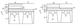
- isolation regions 312 may be formed in a substrate 310 by conventional techniques, which are not described in detail herein.
- a gate oxide material 314 may be formed over the substrate 310 .
- the gate oxide material 314 may be thermally grown or may be deposited, and may include a material such as silicon dioxide. While not shown, other materials may, optionally, intervene between the substrate 310 and the gate oxide material 314 depending on the desired application of the semiconductor structure 300 .
- the substrate 310 may include source and drain regions.
- n-channel region 305 of the substrate 310 may include n-doped source and drain regions 302 and p-channel region 315 may include p-doped source and drain regions 304 located adjacent the isolation regions 312 .
- Source and drain regions 302 may be formed by doping the semiconductor substrate 310 with n-type dopants, such as boron, as known in the art.
- Source and drain regions 304 may be formed by doping the semiconductor substrate 310 with p-type dopants, such as phosphorus, as known in the art.
- a dielectric material 316 may be formed over the gate oxide material 314 .
- the dielectric material 316 may be a dielectric material such as a silicon oxide or a high-k dielectric material similar to high-k dielectric material described above with reference to high-k dielectric material 216 .
- the dielectric material 316 is hafnium oxide.
- the dielectric material 316 may be formed by ALD, CVD, PECVD, LPCVD, PVD, or other film deposition processes.
- a first metal material 318 may be formed over the dielectric material 316 .
- the first metal material 318 may be selected to provide adhesion to the dielectric material 316 .
- the first metal material 318 is a metal nitride, such as titanium nitride.
- the first metal material 318 may have a thickness of between about 10 angstroms (A) and about 30 ⁇ , such as between about 15 ⁇ and about 25 ⁇ . In some embodiments, the first metal material 318 has a thickness of about 20 ⁇ .
- a capping material 320 may overlie the first metal material 318 .
- the capping material 320 may include a metal such as magnesium, magnesium oxide, lanthanum, lanthanum oxide, or combinations thereof. In some embodiments, the capping material 320 is magnesium.
- the capping material 320 may be selected to provide a decreased work function of the NMOS device in n-channel region 305 .
- the capping material 320 may be formed to a thickness of between about 5 ⁇ and about 15 ⁇ , such as between about 5 ⁇ and about 10 ⁇ . In some embodiments, the capping material 320 has a thickness of about 8 ⁇ .
- the capping material 320 may be formed by ALD, CVD, PECVD, LPCVD, PVD, or other deposition processes.
- a second metal material 322 may be formed over the capping material 320 .
- the second metal material 322 may be formed of the same metal as the first metal material 318 .
- the second metal material 322 is titanium nitride.
- the second metal material 322 may include a lower portion foiined of a metal material or metal nitride and an exposed portion formed of a metal nitride.
- a lower portion of the second metal material 322 is a metal material and an exposed portion of the second metal material 322 is titanium nitride.
- the second metal material 322 may be formed to a greater thickness than the first metal material 318 .
- the second metal material 322 may have a thickness of between about 20 ⁇ and about 60 ⁇ , such as between about 30 ⁇ and about 50 ⁇ , or between about 35 ⁇ and about 45 ⁇ . In some embodiments, the second metal material 322 has a thickness of about 40 ⁇ .
- the second metal material 322 may be formed by similar methods as the first metal material 318 .
- the second metal material 322 may be formed by ALD, CVD, PECVD, LPCVD, PVD, or other suitable deposition process.
- the first metal material 318 , capping material 320 , and second metal material 322 may form a gate stack 325 in the n-channel region 305 .
- a mask material 340 and a photoresist material 350 may be formed over the semiconductor structure 300 and patterned to expose the second metal material 322 in the p-channel region 315 of the semiconductor structure 300 .
- the mask material 340 may include a hardmask material or other suitable masking material and may have a thickness of about 15 nm. In some embodiments, the mask material 340 is a silicon nitride hardmask.
- the photoresist material 350 may be any conventional photoresist material.
- the mask material 340 and photoresist material 350 may be patterned by conventional techniques, which are not described in detail herein.
- the second metal material 322 , the capping material 320 , and the first metal material 318 may be removed from the p-channel region 315 by reactive ion etching, such as with an oxygen or a nitrogen based plasma.
- the plasma may be, for example, a mixture including nitrogen, boron trichloride, and argon (N 2 /BCl 3 /Ar), a mixture including nitrogen, methane, and argon (N 2 /CH 4 /Ar), or a mixture including oxygen, chlorine, and helium, (O 2 /Cl 2 /He).
- the second metal material 322 , the capping material 320 , and the first metal material 318 in the p-channel region 315 may be removed with a solution including ammonium hydroxide (NH 4 OH), hydrogen peroxide (H 2 O 2 ), and water.
- the mask material 340 and photoresist material 350 may protect the materials of the n-channel region 305 from being removed.
- the etchant may be nonreactive with the dielectric material 316 and, therefore, the dielectric material 316 may function as an etch stop.
- the dielectric material 316 of p-channel region 315 may be exposed after removing the second metal material 322 , the capping material 320 , and the first metal material 318 .
- the photoresist material 350 and mask material 340 may be removed from n-channel region 305 to expose the second metal material 322 of n-channel region 305 .
- the dielectric material 316 may be crystallized to increase the etch selectivity of the mask material 340 relative to the dielectric material 316 .
- the dielectric material 316 may be annealed to crystallize the dielectric material 316 .
- the mask material 340 may be removed from n-channel region 305 without substantially removing the dielectric material 316 exposed in p-channel region 315 .
- the second metal material 322 may be exposed in the n-channel region.
- an aluminum-containing material 327 may be formed over exposed surfaces of the semiconductor structure 300 .
- the aluminum-containing material 327 may be conformally formed over the dielectric material 316 of p-channel region 315 and over the second metal material 322 of n-channel region 305 .
- the aluminum-containing material 327 may be formed by conventional techniques, such as by an ALD process, a CVD process, a PECVD process, an LPCVD process, a PVD process, or other deposition process, using appropriately selected aluminum precursors and oxygen precursors.
- the aluminum-containing material 327 may form as an aluminum oxide 324 on the dielectric material 316 of p-channel region 315 and as a metal-aluminum compound 326 on the second metal material 322 of n-channel region 305 .
- the aluminum of the aluminum-containing material 327 formed on the second metal material 322 may react with the metal of the second metal material 322 , forming the metal-aluminum compound 326 .
- the metal-aluminum compound 326 may also form on the sidewalls of the gate stack 325 where the first metal material 318 and the second metal material 322 are exposed.
- the metal-aluminum compound 326 may be a reaction product of aluminum from the aluminum-containing material 327 , the metal from the second metal material 322 , oxygen from the aluminum-containing material 327 , and nitrogen from the second metal material 322 .
- the second metal material 322 is titanium nitride.
- the metal-aluminum compound 326 may include aluminum, titanium, nitrogen, and oxygen atoms.
- the aluminum compound 326 is a material such as AlTiO x N y , where x is between one (1) and four (4) and y is between one-half (1 ⁇ 2) and two (2). In other embodiments, x is about 2.5 and y is about 0.8.
- the metal-aluminum compound 326 may include about nineteen atomic percent (19 at. %) of each of aluminum and titanium, about forty-seven atomic percent (47 at. %) of oxygen, and about fifteen atomic percent (15 at. %) of nitrogen.
- exposing the semiconductor substrate 300 to the aluminum precursor and the oxygen precursor may form different aluminum-containing materials on n-channel region 305 and p-channel region 315 of the semiconductor structure 300 .
- Aluminum oxide 324 may be formed on p-channel region 315 and the metal-aluminum compound 326 may be foimed on n-channel region 305 of the semiconductor structure 300 .
- the aluminum oxide 324 and the metal-aluminum compound 326 may be foiined by exposing the semiconductor structure 300 to the aluminum precursor and the oxygen precursor.
- the aluminum oxide 324 and the metal-aluminum compound 326 may be foiined by a deposition process including an aluminum precursor and an oxygen precursor.
- the aluminum precursor may include tris(diethylamino) aluminum (TDEAA), alkyl aluminum precursors such as tri-methyl aluminum (TMA), aluminum alkoxides such as aluminum isopropoxide (AIP), aluminum tri-sec-butoxide (ATSB), aluminum ethoxide, dimethylaluminumhydride (DMAH), aluminum tris(2,2,6,6-tetramethyl-3,5-heptanedionate), triisobutylaluminum (TIBA), tris(dimethylamido)aluminum (III), or combinations thereof.
- the oxygen precursor may include oxygen (O 2 ), ozone (O 3 ), water, or combinations thereof.
- the aluminum precursor is TMA and the oxygen containing precursor is water.
- the aluminum-containing material may be formed by ALD.
- the aluminum-containing material 327 may be formed by performing between one ALD cycle and ten ALD cycles. For example, between one ALD cycle and five ALD cycles or between five ALD cycles and ten ALD cycles may be performed.
- the aluminum oxide 324 may be formed to a thickness of between about 5 ⁇ and about 10 ⁇ , such as between about 5 ⁇ and about 8 ⁇ .
- the metal-aluminum compound 326 may be formed to a greater thickness than the aluminum oxide 324 . Without being bound by any theory, it is believed that the thickness of the metal-aluminum compound 326 may be greater than the thickness of the aluminum oxide 324 because of the incorporation of the second metal material 322 and nitrogen in the metal-aluminum compound 326 .
- the deposition process may be performed at a temperature from between about 200° C. and about 400° C., such as between about 250° C. and about 350° C. In some embodiments, the deposition is performed at a temperature of about 300° C., which enhances the formation of the metal-aluminum compound 326 over the second metal material 322 .
- the aluminum oxide 324 may be formed only in p-channel region 315 and the metal-aluminum compound 326 may be formed only in n-channel region 305 of the semiconductor structure 300 .
- the aluminum oxide 324 may be selectively formed over only the dielectric material 316 of p-channel region 315 .
- the metal-aluminum compound 326 and the aluminum oxide 324 are formed concurrently, the composition of the metal-aluminum compound 326 may be different than the composition of the aluminum oxide 324 .
- the formation of the different aluminum-containing materials may be self-aligned on the respective regions of the semiconductor structure 300 .
- the metal-aluminum compound 326 may be selectively removed from the semiconductor structure 300 such that only the aluminum oxide 324 of the aluminum-containing material 327 ( FIG. 3D ) remains in p-channel region 315 of the semiconductor structure 300 .
- the aluminum oxide 324 and the metal-aluminum compound 326 may exhibit different etch rates when exposed to various etchants.
- the metal-aluminum compound 326 may be removed using an aqueous solution of H 2 O 2 , whereas the aluminum oxide 324 may exhibit a low removal rate upon exposure to the aqueous H 2 O 2 solution.
- the metal-aluminum compound 326 may have an etch rate that is at least about 10 times greater than that of the aluminum oxide 324 when exposed to the H 2 O 2 solution.
- the metal-aluminum compound 326 may be removed by exposing the semiconductor structure 300 to H 2 O 2 .
- exposing the aluminum oxide 324 to the H 2 O 2 solution may not remove any or may remove only a small portion of the aluminum oxide 324 . Because the aluminum oxide 324 is not removed by exposure to the H 2 O 2 solution, the aluminum oxide 324 may also protect underlying materials from being damaged by the H 2 O 2 solution. The H 2 O 2 solution may also clean the surface of the semiconductor structure 300 prior to forming additional materials thereover.
- the metal-aluminum compound 326 may be removed at a rate of approximately 50 ⁇ per minute when exposed to the H 2 O 2 solution.
- an metal-aluminum compound 326 having a thickness of between about 10 ⁇ and about 20 ⁇ may be removed by exposing the metal-aluminum compound 326 to the H 2 O 2 solution for less than approximately one minute, such as less than about thirty seconds.
- the semiconductor structure 300 is exposed to a solution of H 2 O 2 for a period of time ranging from between about ten seconds to about three minutes, such as between about thirty seconds and about one minute, or between about one minute and about two minutes.
- the semiconductor structure 300 is exposed to an H 2 O 2 solution for about one minute to substantially remove the metal-aluminum compound 326 while the aluminum oxide 324 remains in p-channel region 315 .
- the H 2 O 2 solution may be formed of H 2 O 2 and water.
- the H 2 O 2 solution may have a H 2 O 2 concentration ranging from between about one weight percent (1 wt. %) to about ten weight percent (10 wt. %), such as between about three weight percent (3 wt. %) and about seven weight percent (7 wt. %).
- the H 2 O 2 solution includes between about three weight percent (3 wt. %) and about five weight percent (5 wt. %) H 2 O 2 .
- the semiconductor structure 300 may be exposed to the H 2 O 2 solution at a temperature of between about 20° C. and about 100° C., such as between about 25° C. and about 75° C. In some embodiments, the H 2 O 2 solution is applied at a temperature of about room temperature (e.g., between about 20° C. and about 25° C.). In other embodiments, the H 2 O 2 solution is applied at a temperature of about 65° C.
- the aluminum oxide 324 remains on p-channel region 315 of the semiconductor structure 300 while no aluminum-containing material 327 is present on the n-channel region 305 .
- the aluminum oxide 324 may be formed at a desired location on the semiconductor structure 300 and may be self-aligned without using an additional photolithography act to pattern the aluminum oxide 324 .
- the complexity and cost of the method of the present disclosure may be reduced compared to conventional techniques of forming and patterning aluminum oxide 324 .
- the use of extra materials, such as a photoresist and BARC is avoided.
- the methods of embodiments of the present disclosure may also enable reduction in the number of etch acts and etchants used. Since no photoresist and BARC are used, only a single etchant, aqueous H 2 O 2 , is needed, which further reduces the complexity and cost of the methods of embodiments of the present disclosure.
- a conductive material 328 may be conformally formed over the semiconductor structure 300 .
- the conductive material 328 may be formed over the second metal material 322 in n-channel region 305 and over the aluminum oxide 324 in p-channel region 315 .
- the conductive material 328 may be formed by ALD, CVD, PECVD, LPCVD, PVD, or other deposition method.
- the conductive material 328 may have a thickness of between about 40 ⁇ and about 60 ⁇ , such as between about 45 ⁇ and about 55 ⁇ . In some embodiments, the thickness of the conductive material 328 is about 50 ⁇ .
- the conductive material 328 may include a metal or a metal nitride.
- the conductive material 328 may include the same metal as the first metal material 318 or the second metal material 322 .
- the conductive material 328 , the first metal material 318 , and the second metal material 322 are the same material.
- the conductive material 328 is titanium nitride.
- a silicon material 330 may be formed over the conductive material 328 .
- the silicon material 330 may be formed by suitable methods, such as PVD, ALD, CVD, PECVD, LPCVD, PVD, or other deposition methods.
- the silicon material 330 may have a thickness of between about 2 nm and about 10 nm, such as between about 3 nm and about 8 nm, and between about 4 nm and about 6 nm. In some embodiments, the silicon material 330 has a thickness of about 5 nm.
- N-channel region 305 may be implanted with arsenic to form arsenic implanted regions (not shown) at an interface between the first metal material 318 and the capping material 320 and at an interface between the capping material 320 and the second metal material 322 .
- the mask material may be removed from the semiconductor structure 300 .
- a polysilicon material 332 may be formed over the silicon material 330 .
- the polysilicon material 332 may be doped with boron or doped with phosphorus. In some embodiments, the polysilicon material 332 is doped with phosphorus.
- the polysilicon material 332 may be formed by forming polysilicon and then doping with phosphorus, or the polysilicon material 332 may be formed in situ. In some embodiments, the polysilicon material 332 is formed in situ by including dopant gases such as phosphine or diborane in the deposition precursor gas recipe.
- a second conductive material 334 may be formed over the polysilicon material 332 .
- the second conductive material 334 may include a conductive metal such as copper, tungsten, aluminum, titanium, tantalum, platinum, alloys thereof, heavily doped semiconductor material, a conductive silicide, or combinations thereof.
- the second conductive material 334 is tungsten.
- a silicon nitride material 336 may overlie the second conductive material 334 .
- the silicon nitride material 336 may be formed by a suitable deposition process, such as ALD, CVD, PECVD, LPCVD, PVD, or other deposition process.
- Additional processing acts may be performed by conventional techniques to produce a complete semiconductor device, such as a CMOS device or DRAM memory cell, according to the desired end use of the semiconductor structure 300 .
- a method of forming a semiconductor structure comprises exposing a dielectric material and a metal nitride on a substrate to an aluminum precursor and an oxygen precursor to form aluminum oxide over the dielectric material and a metal-aluminum compound over the metal nitride.
- the aluminum oxide and the metal-aluminum compound are exposed to a solution comprising hydrogen peroxide.
- titanium nitride 420 may be formed over a substrate 410 .
- intervening materials between the titanium nitride 420 and the substrate 410 such as at least one of a dielectric material, conductive material, work function modifier, or other materials.
- a conductive material such as copper, tungsten, aluminum, titanium, tantalum, platinum, alloys thereof, heavily doped semiconductor material, a conductive silicide, or combinations thereof may underlie the titanium nitride 420 .
- the titanium nitride 420 may be patterned with a photomask or a hardmask material by conventional techniques, which are not described in detail herein. Desired portions of the titanium nitride 420 may be removed through openings in the mask. For example, the titanium nitride 420 may be exposed to an aqueous solution of H 2 O 2 or a solution of ammonium hydroxide. In some embodiments, the titanium nitride 420 is removed with an H 2 O 2 solution at a rate of about 10 ⁇ per minute.
- an aluminum-containing material 427 may be conformally formed on the semiconductor structure 400 .
- the substrate 410 (or intervening materials, if present) and the titanium nitride 420 may be exposed to the aluminum precursor and the oxygen precursor at a temperature of between about 200° C. and about 400° C., such as between about 250° C. and about 300° C., or between about 300° C. and about 350° C.
- the aluminum-containing material 427 includes a metal-aluminum compound 440 and aluminum oxide 430 . In some embodiments, the temperature is about 300° C.
- Exposing the substrate 410 to the aluminum precursor and the oxygen precursor may form the aluminum oxide 430 over the substrate 410 and the metal-aluminum compound 440 over the titanium nitride 420 .
- the metal-aluminum compound 440 may be AlTiN y O x , where x is between one (1) and four (4) and y is between one-half (1 ⁇ 2) and two (2). In other embodiments, x is about 2.5 and y is about 0.8.
- the metal-aluminum compound 440 may comprise about nineteen atomic percent (19 at. %) of each of aluminum and titanium, about forty-seven atomic percent (47 at. %) of oxygen, and about fifteen atomic percent (15 at. %) of nitrogen.
- the aluminum-containing material 427 is formed by ALD.
- the aluminum-containing material 427 may be formed by performing between one ALD cycle and ten ALD cycles. For example, between one ALD cycle and five ALD cycles or between five ALD cycles and ten ALD cycles may be performed.
- the aluminum oxide 430 may have a thickness of between about 5 ⁇ and about 15 ⁇ , such as between about 5 ⁇ and about 10 ⁇ , or between about 10 ⁇ and about 15 ⁇ .
- the metal-aluminum compound 440 may have a thickness that is greater than the thickness of the aluminum oxide 430 .
- the metal-aluminum compound 440 may be removed by exposing the semiconductor structure 400 to a solution of H 2 O 2 , as described above with reference to FIG. 3E .
- the metal-aluminum compound 440 may be removed by exposing the semiconductor structure 400 to a solution of between about three weight percent (3 wt. %) and about ten weight percent (10 wt. %) H 2 O 2 for between about ten seconds and about three minutes.
- the aluminum oxide 430 may remain on the substrate 410 .
- additional processing acts may be performed to remove the titanium nitride 420 from the semiconductor structure 400 .
- the titanium nitride 420 may be removed at a rate of about 10 ⁇ per minute by exposing the titanium nitride 420 to the H 2 O 2 solution.
- the resulting semiconductor structure 400 may include aluminum oxide 430 on desired portions of the substrate 410 .
- the resulting semiconductor structure 400 may include the intervening materials.
- a method of forming aluminum oxide comprises forming titanium nitride on portions of a substrate.
- a titanium-aluminum compound is formed over the titanium nitride and aluminum oxide is formed over the substrate.
- the titanium-aluminum compound and the aluminum oxide are exposed to hydrogen peroxide to remove the titanium-aluminum compound from over the titanium nitride.
- Titanium nitride 520 may be patterned as described above with reference to FIG. 4A .
- the titanium nitride 520 and a substrate 510 may be exposed to precursors for forming aluminum oxide, such as an aluminum precursor and an oxygen precursor, to form aluminum oxide 530 over the substrate 510 and over the titanium nitride 520 .
- the aluminum oxide 530 may be formed to a thickness greater than about 10 ⁇ , such as up to about 30 ⁇ , up to about 50 ⁇ , or up to about 100 ⁇ .
- Forming greater than about 20 ⁇ of aluminum oxide 530 over a semiconductor structure 500 may form an aluminum oxide 530 over the titanium nitride 520 rather than an metal-aluminum compound 440 as described above with reference to FIG. 4B .
- Aluminum oxide 530 may not be formed over on the sidewalls of the titanium nitride 520 .
- the titanium nitride 520 may be removed by exposing the semiconductor structure 500 to an H 2 O 2 solution.
- the H 2 O 2 solution may remove exposed portions of the titanium nitride 520 , such as side portions extending above the aluminum oxide 530 in between the titanium nitride 520 .
- a self-patterned aluminum oxide 530 having a thickness greater than approximately 10 ⁇ may be formed.
- the aluminum oxide 530 between the titanium nitride 520 may have a thickness that is less than a thickness of the titanium nitride 520 .
- a method of forming an aluminum oxide material comprises subjecting exposed portions of a substrate and titanium nitride to an aluminum precursor and an oxygen precursor to form aluminum oxide on the exposed portions of the substrate and a titanium-aluminum compound on the exposed portions of the titanium nitride.
- the titanium-aluminum compound is removed from the titanium nitride.
- a self-aligned lanthanum oxide (La 2 O 3 ) or magnesium oxide (MgO) may be formed by methods similar to the above disclosed methods of forming aluminum oxide.
- a semiconductor structure may comprise exposed portions of a metal nitride and exposed portions comprising another material.
- the semiconductor structure may be exposed to a lanthanum precursor and an oxygen precursor to form a metal-lanthanum compound over the metal nitride and lanthanum oxide over the other exposed portions of the semiconductor structure.
- the metal-lanthanum compound and the lanthanum oxide may be formed by ALD, CVD, PECVD, LPCVD, PVD, or other deposition process.
- the metal-lanthanum compound may comprise lanthanum, titanium, nitrogen, and oxygen atoms, and may exhibit a different etch rate than the lanthanum oxide upon exposure to various etchants.
- a metal-magnesium compound may be formed over a metal nitride and a magnesium oxide may be formed over other exposed portions of a semiconductor structure by exposing the semiconductor structure to a magnesium precursor and an oxygen precursor.
- the magnesium oxide may be formed by ALD, CVD, PECVD, LPCVD, PVD, or other deposition process.
- a titanium-magnesium compound comprising magnesium, titanium, nitrogen, and oxygen may be formed over the titanium nitride and magnesium oxide may be fomied over other exposed portions of the semiconductor structure.
Landscapes
- Engineering & Computer Science (AREA)
- Physics & Mathematics (AREA)
- Power Engineering (AREA)
- Condensed Matter Physics & Semiconductors (AREA)
- General Physics & Mathematics (AREA)
- Manufacturing & Machinery (AREA)
- Computer Hardware Design (AREA)
- Microelectronics & Electronic Packaging (AREA)
- Chemical & Material Sciences (AREA)
- Chemical Kinetics & Catalysis (AREA)
- General Chemical & Material Sciences (AREA)
- Insulated Gate Type Field-Effect Transistor (AREA)
- Internal Circuitry In Semiconductor Integrated Circuit Devices (AREA)
- Materials Engineering (AREA)
- Crystallography & Structural Chemistry (AREA)
- Composite Materials (AREA)
- Inorganic Chemistry (AREA)
- Plasma & Fusion (AREA)
- Semiconductor Memories (AREA)
- Formation Of Insulating Films (AREA)
Abstract
Description
Claims (20)
Priority Applications (2)
| Application Number | Priority Date | Filing Date | Title |
|---|---|---|---|
| US14/184,452 US9129798B1 (en) | 2014-02-19 | 2014-02-19 | Methods of forming semiconductor structures comprising aluminum oxide |
| US14/826,447 US9450067B2 (en) | 2014-02-19 | 2015-08-14 | Semiconductor devices comprising aluminum oxide |
Applications Claiming Priority (1)
| Application Number | Priority Date | Filing Date | Title |
|---|---|---|---|
| US14/184,452 US9129798B1 (en) | 2014-02-19 | 2014-02-19 | Methods of forming semiconductor structures comprising aluminum oxide |
Related Child Applications (1)
| Application Number | Title | Priority Date | Filing Date |
|---|---|---|---|
| US14/826,447 Division US9450067B2 (en) | 2014-02-19 | 2015-08-14 | Semiconductor devices comprising aluminum oxide |
Publications (2)
| Publication Number | Publication Date |
|---|---|
| US20150235841A1 US20150235841A1 (en) | 2015-08-20 |
| US9129798B1 true US9129798B1 (en) | 2015-09-08 |
Family
ID=53798708
Family Applications (2)
| Application Number | Title | Priority Date | Filing Date |
|---|---|---|---|
| US14/184,452 Active US9129798B1 (en) | 2014-02-19 | 2014-02-19 | Methods of forming semiconductor structures comprising aluminum oxide |
| US14/826,447 Active US9450067B2 (en) | 2014-02-19 | 2015-08-14 | Semiconductor devices comprising aluminum oxide |
Family Applications After (1)
| Application Number | Title | Priority Date | Filing Date |
|---|---|---|---|
| US14/826,447 Active US9450067B2 (en) | 2014-02-19 | 2015-08-14 | Semiconductor devices comprising aluminum oxide |
Country Status (1)
| Country | Link |
|---|---|
| US (2) | US9129798B1 (en) |
Cited By (1)
| Publication number | Priority date | Publication date | Assignee | Title |
|---|---|---|---|---|
| US10358719B2 (en) | 2016-11-23 | 2019-07-23 | Applied Materials, Inc. | Selective deposition of aluminum oxide on metal surfaces |
Families Citing this family (3)
| Publication number | Priority date | Publication date | Assignee | Title |
|---|---|---|---|---|
| US10957644B2 (en) * | 2018-02-02 | 2021-03-23 | Micron Technology, Inc. | Integrated structures with conductive regions having at least one element from group 2 of the periodic table |
| WO2022005696A1 (en) * | 2020-07-03 | 2022-01-06 | Applied Materials, Inc. | Methods for refurbishing aerospace components |
| TW202248447A (en) * | 2021-03-08 | 2022-12-16 | 荷蘭商Asm Ip私人控股有限公司 | Methods and systems for forming a layer comprising aluminum, titanium, and carbon |
Citations (8)
| Publication number | Priority date | Publication date | Assignee | Title |
|---|---|---|---|---|
| US20070098892A1 (en) * | 2005-08-31 | 2007-05-03 | Samsung Electronics Co., Ltd. | Method of forming a layer and method of manufacturing a capacitor using the same |
| US20080113160A1 (en) | 2006-11-14 | 2008-05-15 | Glimmerglass Networks, Inc. | Method And Apparatus For Localized Bonding |
| US20080272438A1 (en) | 2007-05-02 | 2008-11-06 | Doris Bruce B | CMOS Circuits with High-K Gate Dielectric |
| US7592678B2 (en) | 2004-06-17 | 2009-09-22 | Infineon Technologies Ag | CMOS transistors with dual high-k gate dielectric and methods of manufacture thereof |
| US7598142B2 (en) | 2007-03-15 | 2009-10-06 | Pushkar Ranade | CMOS device with dual-epi channels and self-aligned contacts |
| US20130154019A1 (en) | 2011-12-16 | 2013-06-20 | International Business Machines Corporation | Low threshold voltage cmos device |
| US8530974B2 (en) | 2011-09-08 | 2013-09-10 | International Business Machines Corporation | CMOS structure having multiple threshold voltage devices |
| US8536654B2 (en) | 2010-01-13 | 2013-09-17 | Texas Instruments Incorporated | Structure and method for dual work function metal gate CMOS with selective capping |
Family Cites Families (1)
| Publication number | Priority date | Publication date | Assignee | Title |
|---|---|---|---|---|
| US20100213555A1 (en) * | 2009-02-23 | 2010-08-26 | Advanced Micro Devices, Inc. | Metal oxide semiconductor devices having capping layers and methods for fabricating the same |
-
2014
- 2014-02-19 US US14/184,452 patent/US9129798B1/en active Active
-
2015
- 2015-08-14 US US14/826,447 patent/US9450067B2/en active Active
Patent Citations (8)
| Publication number | Priority date | Publication date | Assignee | Title |
|---|---|---|---|---|
| US7592678B2 (en) | 2004-06-17 | 2009-09-22 | Infineon Technologies Ag | CMOS transistors with dual high-k gate dielectric and methods of manufacture thereof |
| US20070098892A1 (en) * | 2005-08-31 | 2007-05-03 | Samsung Electronics Co., Ltd. | Method of forming a layer and method of manufacturing a capacitor using the same |
| US20080113160A1 (en) | 2006-11-14 | 2008-05-15 | Glimmerglass Networks, Inc. | Method And Apparatus For Localized Bonding |
| US7598142B2 (en) | 2007-03-15 | 2009-10-06 | Pushkar Ranade | CMOS device with dual-epi channels and self-aligned contacts |
| US20080272438A1 (en) | 2007-05-02 | 2008-11-06 | Doris Bruce B | CMOS Circuits with High-K Gate Dielectric |
| US8536654B2 (en) | 2010-01-13 | 2013-09-17 | Texas Instruments Incorporated | Structure and method for dual work function metal gate CMOS with selective capping |
| US8530974B2 (en) | 2011-09-08 | 2013-09-10 | International Business Machines Corporation | CMOS structure having multiple threshold voltage devices |
| US20130154019A1 (en) | 2011-12-16 | 2013-06-20 | International Business Machines Corporation | Low threshold voltage cmos device |
Non-Patent Citations (1)
| Title |
|---|
| Chou et al., Imprint of Sub-25 nm Vias and Trenches in Polymers, Appl. Phys. Lett., vol. 67, No. 21, Nov. 20, 1995, pp. 3114-3116. |
Cited By (2)
| Publication number | Priority date | Publication date | Assignee | Title |
|---|---|---|---|---|
| US10358719B2 (en) | 2016-11-23 | 2019-07-23 | Applied Materials, Inc. | Selective deposition of aluminum oxide on metal surfaces |
| US11060188B2 (en) | 2016-11-23 | 2021-07-13 | Applied Materials, Inc. | Selective deposition of aluminum oxide on metal surfaces |
Also Published As
| Publication number | Publication date |
|---|---|
| US9450067B2 (en) | 2016-09-20 |
| US20150235841A1 (en) | 2015-08-20 |
| US20150349082A1 (en) | 2015-12-03 |
Similar Documents
| Publication | Publication Date | Title |
|---|---|---|
| US10367062B2 (en) | Co-integration of silicon and silicon-germanium channels for nanosheet devices | |
| US6667246B2 (en) | Wet-etching method and method for manufacturing semiconductor device | |
| US9252058B2 (en) | Semiconductor device and method of fabricating the same | |
| US10109534B2 (en) | Multi-threshold voltage (Vt) workfunction metal by selective atomic layer deposition (ALD) | |
| CN109427873A (en) | The structures and methods of metal gates with coarse barrier layer | |
| US8846540B2 (en) | Semiconductor device with silicon-containing hard mask and method for fabricating the same | |
| US10504795B2 (en) | Method for patterning a lanthanum containing layer | |
| US9450067B2 (en) | Semiconductor devices comprising aluminum oxide | |
| TWI478246B (en) | Forming a channel semiconductor alloy by forming a hard mask layer stack and using a plasma-based mask patterning process | |
| US20110217833A1 (en) | Method of manufacturing a semiconductor device using an etchant | |
| US10224329B2 (en) | Forming gates with varying length using sidewall image transfer | |
| US10020202B2 (en) | Fabrication of multi threshold-voltage devices | |
| US7323419B2 (en) | Method of fabricating semiconductor device | |
| US9018066B2 (en) | Method of fabricating semiconductor device structure | |
| JP2007036116A (en) | Semiconductor device manufacturing method | |
| US12494423B2 (en) | Semiconductor device including stacked via contact and method for manufacturing the same | |
| JP2011187498A (en) | Semiconductor device manufacturing method | |
| CN101355029B (en) | Method for forming grids of semiconductor device | |
| CN113097136A (en) | Method for forming semiconductor structure | |
| KR20120039136A (en) | Method of manufacturing a semiconductor device | |
| WO2011104788A1 (en) | Method for manufacturing a semiconductor device |
Legal Events
| Date | Code | Title | Description |
|---|---|---|---|
| AS | Assignment |
Owner name: MICRON TECHNOLOGY, INC., IDAHO Free format text: ASSIGNMENT OF ASSIGNORS INTEREST;ASSIGNOR:ZHU, DIFENG;REEL/FRAME:032248/0939 Effective date: 20140218 |
|
| FEPP | Fee payment procedure |
Free format text: PAYOR NUMBER ASSIGNED (ORIGINAL EVENT CODE: ASPN); ENTITY STATUS OF PATENT OWNER: LARGE ENTITY |
|
| STCF | Information on status: patent grant |
Free format text: PATENTED CASE |
|
| CC | Certificate of correction | ||
| AS | Assignment |
Owner name: U.S. BANK NATIONAL ASSOCIATION, AS COLLATERAL AGENT, CALIFORNIA Free format text: SECURITY INTEREST;ASSIGNOR:MICRON TECHNOLOGY, INC.;REEL/FRAME:038669/0001 Effective date: 20160426 Owner name: U.S. BANK NATIONAL ASSOCIATION, AS COLLATERAL AGEN Free format text: SECURITY INTEREST;ASSIGNOR:MICRON TECHNOLOGY, INC.;REEL/FRAME:038669/0001 Effective date: 20160426 |
|
| AS | Assignment |
Owner name: MORGAN STANLEY SENIOR FUNDING, INC., AS COLLATERAL AGENT, MARYLAND Free format text: PATENT SECURITY AGREEMENT;ASSIGNOR:MICRON TECHNOLOGY, INC.;REEL/FRAME:038954/0001 Effective date: 20160426 Owner name: MORGAN STANLEY SENIOR FUNDING, INC., AS COLLATERAL Free format text: PATENT SECURITY AGREEMENT;ASSIGNOR:MICRON TECHNOLOGY, INC.;REEL/FRAME:038954/0001 Effective date: 20160426 |
|
| AS | Assignment |
Owner name: U.S. BANK NATIONAL ASSOCIATION, AS COLLATERAL AGENT, CALIFORNIA Free format text: CORRECTIVE ASSIGNMENT TO CORRECT THE REPLACE ERRONEOUSLY FILED PATENT #7358718 WITH THE CORRECT PATENT #7358178 PREVIOUSLY RECORDED ON REEL 038669 FRAME 0001. ASSIGNOR(S) HEREBY CONFIRMS THE SECURITY INTEREST;ASSIGNOR:MICRON TECHNOLOGY, INC.;REEL/FRAME:043079/0001 Effective date: 20160426 Owner name: U.S. BANK NATIONAL ASSOCIATION, AS COLLATERAL AGEN Free format text: CORRECTIVE ASSIGNMENT TO CORRECT THE REPLACE ERRONEOUSLY FILED PATENT #7358718 WITH THE CORRECT PATENT #7358178 PREVIOUSLY RECORDED ON REEL 038669 FRAME 0001. ASSIGNOR(S) HEREBY CONFIRMS THE SECURITY INTEREST;ASSIGNOR:MICRON TECHNOLOGY, INC.;REEL/FRAME:043079/0001 Effective date: 20160426 |
|
| AS | Assignment |
Owner name: JPMORGAN CHASE BANK, N.A., AS COLLATERAL AGENT, ILLINOIS Free format text: SECURITY INTEREST;ASSIGNORS:MICRON TECHNOLOGY, INC.;MICRON SEMICONDUCTOR PRODUCTS, INC.;REEL/FRAME:047540/0001 Effective date: 20180703 Owner name: JPMORGAN CHASE BANK, N.A., AS COLLATERAL AGENT, IL Free format text: SECURITY INTEREST;ASSIGNORS:MICRON TECHNOLOGY, INC.;MICRON SEMICONDUCTOR PRODUCTS, INC.;REEL/FRAME:047540/0001 Effective date: 20180703 |
|
| AS | Assignment |
Owner name: MICRON TECHNOLOGY, INC., IDAHO Free format text: RELEASE BY SECURED PARTY;ASSIGNOR:U.S. BANK NATIONAL ASSOCIATION, AS COLLATERAL AGENT;REEL/FRAME:047243/0001 Effective date: 20180629 |
|
| MAFP | Maintenance fee payment |
Free format text: PAYMENT OF MAINTENANCE FEE, 4TH YEAR, LARGE ENTITY (ORIGINAL EVENT CODE: M1551); ENTITY STATUS OF PATENT OWNER: LARGE ENTITY Year of fee payment: 4 |
|
| AS | Assignment |
Owner name: MICRON TECHNOLOGY, INC., IDAHO Free format text: RELEASE BY SECURED PARTY;ASSIGNOR:MORGAN STANLEY SENIOR FUNDING, INC., AS COLLATERAL AGENT;REEL/FRAME:050937/0001 Effective date: 20190731 |
|
| AS | Assignment |
Owner name: MICRON SEMICONDUCTOR PRODUCTS, INC., IDAHO Free format text: RELEASE BY SECURED PARTY;ASSIGNOR:JPMORGAN CHASE BANK, N.A., AS COLLATERAL AGENT;REEL/FRAME:051028/0001 Effective date: 20190731 Owner name: MICRON TECHNOLOGY, INC., IDAHO Free format text: RELEASE BY SECURED PARTY;ASSIGNOR:JPMORGAN CHASE BANK, N.A., AS COLLATERAL AGENT;REEL/FRAME:051028/0001 Effective date: 20190731 |
|
| MAFP | Maintenance fee payment |
Free format text: PAYMENT OF MAINTENANCE FEE, 8TH YEAR, LARGE ENTITY (ORIGINAL EVENT CODE: M1552); ENTITY STATUS OF PATENT OWNER: LARGE ENTITY Year of fee payment: 8 |