US9124014B2 - Audio jack connector with small size for space saving - Google Patents
Audio jack connector with small size for space saving Download PDFInfo
- Publication number
- US9124014B2 US9124014B2 US13/834,545 US201313834545A US9124014B2 US 9124014 B2 US9124014 B2 US 9124014B2 US 201313834545 A US201313834545 A US 201313834545A US 9124014 B2 US9124014 B2 US 9124014B2
- Authority
- US
- United States
- Prior art keywords
- contacts
- contact
- housing
- electrical connector
- receiving channel
- Prior art date
- Legal status (The legal status is an assumption and is not a legal conclusion. Google has not performed a legal analysis and makes no representation as to the accuracy of the status listed.)
- Active, expires
Links
- 238000003780 insertion Methods 0.000 claims description 8
- 230000037431 insertion Effects 0.000 claims description 8
- 238000005476 soldering Methods 0.000 abstract description 17
- 230000000717 retained effect Effects 0.000 abstract description 5
- 230000013011 mating Effects 0.000 description 5
- 230000002452 interceptive effect Effects 0.000 description 1
- 238000012986 modification Methods 0.000 description 1
- 230000004048 modification Effects 0.000 description 1
- 230000005236 sound signal Effects 0.000 description 1
Images


Classifications
-
- H—ELECTRICITY
- H01—ELECTRIC ELEMENTS
- H01R—ELECTRICALLY-CONDUCTIVE CONNECTIONS; STRUCTURAL ASSOCIATIONS OF A PLURALITY OF MUTUALLY-INSULATED ELECTRICAL CONNECTING ELEMENTS; COUPLING DEVICES; CURRENT COLLECTORS
- H01R13/00—Details of coupling devices of the kinds covered by groups H01R12/70 or H01R24/00 - H01R33/00
- H01R13/40—Securing contact members in or to a base or case; Insulating of contact members
- H01R13/405—Securing in non-demountable manner, e.g. moulding, riveting
- H01R13/41—Securing in non-demountable manner, e.g. moulding, riveting by frictional grip in grommet, panel or base
-
- H—ELECTRICITY
- H01—ELECTRIC ELEMENTS
- H01R—ELECTRICALLY-CONDUCTIVE CONNECTIONS; STRUCTURAL ASSOCIATIONS OF A PLURALITY OF MUTUALLY-INSULATED ELECTRICAL CONNECTING ELEMENTS; COUPLING DEVICES; CURRENT COLLECTORS
- H01R24/00—Two-part coupling devices, or either of their cooperating parts, characterised by their overall structure
- H01R24/58—Contacts spaced along longitudinal axis of engagement
-
- H—ELECTRICITY
- H01—ELECTRIC ELEMENTS
- H01R—ELECTRICALLY-CONDUCTIVE CONNECTIONS; STRUCTURAL ASSOCIATIONS OF A PLURALITY OF MUTUALLY-INSULATED ELECTRICAL CONNECTING ELEMENTS; COUPLING DEVICES; CURRENT COLLECTORS
- H01R12/00—Structural associations of a plurality of mutually-insulated electrical connecting elements, specially adapted for printed circuits, e.g. printed circuit boards [PCB], flat or ribbon cables, or like generally planar structures, e.g. terminal strips, terminal blocks; Coupling devices specially adapted for printed circuits, flat or ribbon cables, or like generally planar structures; Terminals specially adapted for contact with, or insertion into, printed circuits, flat or ribbon cables, or like generally planar structures
- H01R12/70—Coupling devices
- H01R12/71—Coupling devices for rigid printing circuits or like structures
- H01R12/712—Coupling devices for rigid printing circuits or like structures co-operating with the surface of the printed circuit or with a coupling device exclusively provided on the surface of the printed circuit
- H01R12/716—Coupling device provided on the PCB
-
- H—ELECTRICITY
- H01—ELECTRIC ELEMENTS
- H01R—ELECTRICALLY-CONDUCTIVE CONNECTIONS; STRUCTURAL ASSOCIATIONS OF A PLURALITY OF MUTUALLY-INSULATED ELECTRICAL CONNECTING ELEMENTS; COUPLING DEVICES; CURRENT COLLECTORS
- H01R24/00—Two-part coupling devices, or either of their cooperating parts, characterised by their overall structure
- H01R24/38—Two-part coupling devices, or either of their cooperating parts, characterised by their overall structure having concentrically or coaxially arranged contacts
- H01R24/40—Two-part coupling devices, or either of their cooperating parts, characterised by their overall structure having concentrically or coaxially arranged contacts specially adapted for high frequency
- H01R24/50—Two-part coupling devices, or either of their cooperating parts, characterised by their overall structure having concentrically or coaxially arranged contacts specially adapted for high frequency mounted on a PCB [Printed Circuit Board]
Definitions
- the present invention relates generally to an audio jack connector, and more particularly to an audio jack connector with small size for space saving purpose.
- a multipolar plug is used to receive audio signals from a plurality of electrical devices such as mobile phones, MP3s, and so on.
- the electrical device usually has an audio jack connector receiving the audio plug.
- the audio jack connector comprises an insulative housing and a plurality of contacts retained in the insulative housing.
- the insulative housing defines a receiving channel for the audio plug.
- the contacts are arranged at two sides of the receiving channel. Each contact has a contacting portion engaging with the audio plug.
- the contacts at the same side are not so configured as to intersect with each other for the purpose of saving space.
- 201303089 discloses an audio jack connector comprising a pair of switch terminals that intersect with each other along a transverse direction perpendicular to a mating direction along which an audio plug is inserted.
- the switch terminals comprise an immovable contact and a movable contact.
- the immovable contact is retained in the insulative housing.
- the immovable contact has a first contacting portion detachably engaged with a second contacting portion of the movable contact for detecting purpose.
- the first contacting portion of the immovable contact does not extend into a receiving channel of the insulative housing for contacting with the audio plug.
- an object of the present invention is to provide an audio jack connector for space saving purpose.
- an audio jack connector includes an insulative housing, a first contact and a second contact retained in the insulative housing.
- the insulative housing defines a receiving channel.
- the first contact includes a first retaining portion, a first soldering portion bent laterally from the first retaining portion, and a first contacting portion extending from the first retaining portion.
- the second contact includes a second contacting portion extending into the receiving channel, an upper beam and a lower beam forkedly, backwardly extending from the contacting portion, a hook portion formed at the distal end of the upper beam and secured with the insulative housing, and a second soldering portion bent laterally from the lower beam.
- An interspace is defined between the upper beam and the lower beam and the first contacting portion protrudes into the receiving channel via the interspace.
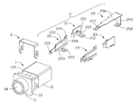
- FIG. 1 is a perspective, assembled view of an audio jack connector according to the present invention
- FIG. 2 is another perspective, assembled view of the audio jack connector
- FIG. 3 is a perspective, exploded view of the audio jack connector
- FIG. 4 is another perspective, exploded view of the audio jack connector
- FIG. 5 is a cross-sectional view of FIG. 2 when taken along line 5 - 5 ;
- FIG. 6 is a cross-sectional view of FIG. 1 when taken along line 6 - 6 .
- an audio jack connector 100 of the present invention comprises an insulative housing 1 , a plurality of contacts 2 retained in the insulative housing 1 , and a securing board 3 assembled to the insulative housing 1 for assembling the insulative housing 1 on a printed circuit board (not shown).
- the insulative housing 1 comprises a circular head portion 11 , a rectangular base portion 12 , and a neck portion 13 connected between the head portion 11 and the base portion 12 .
- the insulative housing 1 defines a receiving channel 14 extending through the head portion 11 , the neck portion 13 , and the base portion 12 .
- the base portion 12 defines a plurality of terminal passageways 121 communicating with the receiving channel 14 .
- the base portion 12 defines a recess portion 122 adjacent to the neck portion 13 .
- the securing board 3 is secured in the recess portion 122 .
- the neck portion 13 protrudes out of the head portion 11 and the base portion 12 .
- the insulative housing 1 defines an insertion opening (not labeled) on the head portion 11 which communicates with the receiving channel 14 , a rear face opposite to the insertion opening and a mounting face abutting the printed circuit board. Therefore, a mating direction is defined by the insertion opening.
- the mounting face forms a pair of protrusions 15 .
- the protrusions 15 and the securing board 3 are both fixed to the printed circuit board.
- the contacts 2 comprises a first contact 21 and a second contact 22 both at a left side of the receiving channel 14 , a third contact 23 and a fourth contact 24 both at a right side of the receiving channel 14 , and a fifth contact 25 at an upper side of the receiving channel 14 .
- the first contact 21 comprises a first retaining portion 211 , a first soldering portion 212 bent laterally from a lower edge of the first retaining portion 211 , and a first contacting portion 213 extending reversely from a front edge of the first retaining portion 211 into the receiving channel 14 .
- the second contact 22 comprises a second contacting portion 221 extending into the receiving channel 14 , an upper beam 222 and a lower beam 223 forkedly, backwardly extending from the contacting portion 221 , a hook portion 224 formed at the distal end of the upper beam 222 , and a second soldering portion 225 bent laterally from the lower beam 223 .
- the upper beam 222 and the lower beam 223 are flexible.
- the hook portion 224 is used for securing with the insulative housing 1 and therefore, the upper beam 222 is prevented from dropping down due to its own weight.
- An interspace 226 is defined between the upper beam 222 and the lower beam 223 .
- the first contacting portion 213 protrudes into the receiving channel 14 via the interspace 226 . Therefore, the second contact 22 and the first contact 21 intersect with each other along a transverse direction perpendicular to the mating direction.
- the fifth contact 25 comprises a flatly and forwardly extending fifth retaining portion 256 , a fifth contacting portion 257 extending forwardly from the fifth retaining portion 256 into the receiving channel 14 , a fifth soldering portion 257 extending forwardly as the fifth retaining portion 256 but be arranged at a level lower than the fifth retaining portion 256 , and a vertically extending connecting portion 259 connected between the fifth retaining portion 256 and the fifth soldering portion 257 .
- the fifth contact 25 is a grounding contact. Take a view along the mating direction, the fifth contacting portion 257 is the nearest to the insertion hole for timely releasing electrostatic charge.
- Each contact 2 has a soldering portion (such as the first soldering portion 212 of the first contact 21 , the second soldering portion 225 of the second contact portion 22 , and the fifth soldering portion 257 of the fifth contact 25 , while a third soldering portion of the third contact 23 and a fourth soldering portion of the fourth contact 24 are both not labeled), and all of the soldering portions are exposed on the mounting face of the insulative housing 1 in two lines, which facilitates soldering the soldering portions on the printed circuit board.
- a soldering portion such as the first soldering portion 212 of the first contact 21 , the second soldering portion 225 of the second contact portion 22 , and the fifth soldering portion 257 of the fifth contact 25 , while a third soldering portion of the third contact 23 and a fourth soldering portion of the fourth contact 24 are both not labeled
- the upper beam 222 has a small width which induces that the upper beam 222 is flexible and prone to deflect towards the lower beam 223 .
- the first contact 21 and the second contact 22 intersect with each other for space saving purpose and the first contacting portion 213 extends into the receiving channel 14 via the interface 226 , the hook portion 224 of the second contact 22 which connects with the upper beam 223 and engages with the insulative housing 1 prevents the upper beam 223 from deflecting towards the lower beam 223 , and therefore, prevents the first contact 21 and the second contact 22 from interfering with each other.
- the third contact 23 has a same structure with respect to the first contact 21 and the fourth contact 24 has a same structure with respect to the second contact 22 , except the size. Therefore, the fourth contact 24 and the third contact 23 intersect with each other along a transverse direction perpendicular to the mating direction, too. Therefore, a transverse size of the audio jack connector 100 is reduced.
Landscapes
- Coupling Device And Connection With Printed Circuit (AREA)
- Multi-Conductor Connections (AREA)
Abstract
Description
Claims (20)
Applications Claiming Priority (3)
| Application Number | Priority Date | Filing Date | Title |
|---|---|---|---|
| CN201210070025.XA CN102623825B (en) | 2012-03-16 | 2012-03-16 | Audio connector |
| CN201210070025 | 2012-03-16 | ||
| CN201210070025.X | 2012-03-16 |
Publications (2)
| Publication Number | Publication Date |
|---|---|
| US20130244498A1 US20130244498A1 (en) | 2013-09-19 |
| US9124014B2 true US9124014B2 (en) | 2015-09-01 |
Family
ID=46563585
Family Applications (1)
| Application Number | Title | Priority Date | Filing Date |
|---|---|---|---|
| US13/834,545 Active 2033-06-19 US9124014B2 (en) | 2012-03-16 | 2013-03-15 | Audio jack connector with small size for space saving |
Country Status (2)
| Country | Link |
|---|---|
| US (1) | US9124014B2 (en) |
| CN (1) | CN102623825B (en) |
Cited By (3)
| Publication number | Priority date | Publication date | Assignee | Title |
|---|---|---|---|---|
| US20150295335A1 (en) * | 2014-04-10 | 2015-10-15 | Foxconn Interconnect Technology Limited | Electrical connector with improved contacts |
| US20210313725A1 (en) * | 2020-04-01 | 2021-10-07 | Honeywell International Inc. | Electrical connector for a controller |
| USD1078308S1 (en) | 2022-06-13 | 2025-06-10 | Honeywell International Inc. | I/O adaptor module for use with a building controller |
Families Citing this family (5)
| Publication number | Priority date | Publication date | Assignee | Title |
|---|---|---|---|---|
| CN103943987A (en) * | 2013-01-22 | 2014-07-23 | 富士康(昆山)电脑接插件有限公司 | Audio connector and manufacturing method thereof |
| US9397449B2 (en) * | 2013-08-21 | 2016-07-19 | Hon Hai Precision Industry Co., Ltd. | Receptacle connector flexibly connected to a mother board |
| US9583899B2 (en) | 2015-04-23 | 2017-02-28 | Microsoft Technology Licensing, Llc | Apparatus for receiving a signal plug |
| USD937782S1 (en) * | 2018-05-22 | 2021-12-07 | Switchcraft, Inc. | Stereo connector |
| CN118299836B (en) * | 2024-04-26 | 2025-02-18 | 茂硕电源科技股份有限公司 | Electric connector, driving power supply and lighting equipment |
Citations (12)
| Publication number | Priority date | Publication date | Assignee | Title |
|---|---|---|---|---|
| US6575793B1 (en) * | 2001-12-26 | 2003-06-10 | Hon Hai Precision Ind. Co., Ltd. | Audio jack connector |
| US6595804B2 (en) * | 2000-10-30 | 2003-07-22 | Hosiden Corporation | Multipolar jack, a multipolar plug, and a structure for connecting a multipolar jack with a multipolar plug |
| US6676451B2 (en) * | 2000-10-30 | 2004-01-13 | Smk Corporation | Connective jack |
| US6790095B2 (en) * | 2002-08-08 | 2004-09-14 | Richard Liu | Analog and digital audio connector |
| US7033226B1 (en) * | 2005-01-14 | 2006-04-25 | Advanced Connectek Inc. | Audio receptacle connector |
| US7094088B2 (en) * | 2004-12-14 | 2006-08-22 | Hon Hai Precision Ind. Co., Ltd. | Electrical connector having improved connection |
| US7361062B2 (en) * | 2005-12-28 | 2008-04-22 | Hon Hai Precision Ind. Co., Ltd. | Electrical connector with improved soldering characteristic to be mounted on a printed circuit board |
| US7553194B2 (en) * | 2007-03-20 | 2009-06-30 | Hon Hai Precision Ind. Co., Ltd. | Electrical connector |
| US7566242B2 (en) * | 2007-03-02 | 2009-07-28 | Hon Hai Precision Ind. Co., Ltd. | Electrical connector with improved contacts |
| US7726990B2 (en) * | 2007-07-03 | 2010-06-01 | Hon Hai Precision Ind. Co., Ltd. | Electrical connector having improved terminal switch arrangement |
| US7753738B2 (en) * | 2007-06-11 | 2010-07-13 | Hon Hai Precision Ind. Co., Ltd. | Electrical connector with an anti-dust device to avoid the poor contact from dust |
| US20100279553A1 (en) | 2007-12-06 | 2010-11-04 | Ex Company Limited | Multiconductor Jack and Multiconductor Plug |
Family Cites Families (3)
| Publication number | Priority date | Publication date | Assignee | Title |
|---|---|---|---|---|
| CN201113048Y (en) * | 2007-06-19 | 2008-09-10 | 富士康(昆山)电脑接插件有限公司 | electrical connector |
| CN201436736U (en) * | 2009-05-22 | 2010-04-07 | 富港电子(东莞)有限公司 | audio socket connector |
| US7963784B1 (en) * | 2010-08-30 | 2011-06-21 | Cheng Uei Precision Industry Co., Ltd. | Audio jack connector |
-
2012
- 2012-03-16 CN CN201210070025.XA patent/CN102623825B/en active Active
-
2013
- 2013-03-15 US US13/834,545 patent/US9124014B2/en active Active
Patent Citations (12)
| Publication number | Priority date | Publication date | Assignee | Title |
|---|---|---|---|---|
| US6595804B2 (en) * | 2000-10-30 | 2003-07-22 | Hosiden Corporation | Multipolar jack, a multipolar plug, and a structure for connecting a multipolar jack with a multipolar plug |
| US6676451B2 (en) * | 2000-10-30 | 2004-01-13 | Smk Corporation | Connective jack |
| US6575793B1 (en) * | 2001-12-26 | 2003-06-10 | Hon Hai Precision Ind. Co., Ltd. | Audio jack connector |
| US6790095B2 (en) * | 2002-08-08 | 2004-09-14 | Richard Liu | Analog and digital audio connector |
| US7094088B2 (en) * | 2004-12-14 | 2006-08-22 | Hon Hai Precision Ind. Co., Ltd. | Electrical connector having improved connection |
| US7033226B1 (en) * | 2005-01-14 | 2006-04-25 | Advanced Connectek Inc. | Audio receptacle connector |
| US7361062B2 (en) * | 2005-12-28 | 2008-04-22 | Hon Hai Precision Ind. Co., Ltd. | Electrical connector with improved soldering characteristic to be mounted on a printed circuit board |
| US7566242B2 (en) * | 2007-03-02 | 2009-07-28 | Hon Hai Precision Ind. Co., Ltd. | Electrical connector with improved contacts |
| US7553194B2 (en) * | 2007-03-20 | 2009-06-30 | Hon Hai Precision Ind. Co., Ltd. | Electrical connector |
| US7753738B2 (en) * | 2007-06-11 | 2010-07-13 | Hon Hai Precision Ind. Co., Ltd. | Electrical connector with an anti-dust device to avoid the poor contact from dust |
| US7726990B2 (en) * | 2007-07-03 | 2010-06-01 | Hon Hai Precision Ind. Co., Ltd. | Electrical connector having improved terminal switch arrangement |
| US20100279553A1 (en) | 2007-12-06 | 2010-11-04 | Ex Company Limited | Multiconductor Jack and Multiconductor Plug |
Cited By (7)
| Publication number | Priority date | Publication date | Assignee | Title |
|---|---|---|---|---|
| US20150295335A1 (en) * | 2014-04-10 | 2015-10-15 | Foxconn Interconnect Technology Limited | Electrical connector with improved contacts |
| US9484654B2 (en) * | 2014-04-10 | 2016-11-01 | Foxconn Interconnect Technology Limited | Electrical connector with improved contacts |
| US20210313725A1 (en) * | 2020-04-01 | 2021-10-07 | Honeywell International Inc. | Electrical connector for a controller |
| US11183788B2 (en) * | 2020-04-01 | 2021-11-23 | Honeywell International Inc. | Electrical connector for a controller |
| US20220059960A1 (en) * | 2020-04-01 | 2022-02-24 | Honeywell International Inc. | Electrical connector for a controller |
| US11777242B2 (en) * | 2020-04-01 | 2023-10-03 | Honeywell International Inc. | Electrical connector for a controller |
| USD1078308S1 (en) | 2022-06-13 | 2025-06-10 | Honeywell International Inc. | I/O adaptor module for use with a building controller |
Also Published As
| Publication number | Publication date |
|---|---|
| CN102623825B (en) | 2015-04-01 |
| US20130244498A1 (en) | 2013-09-19 |
| CN102623825A (en) | 2012-08-01 |
Similar Documents
| Publication | Publication Date | Title |
|---|---|---|
| US9124014B2 (en) | Audio jack connector with small size for space saving | |
| US9214766B1 (en) | Electrical connector having a metallic inner shell between a metallic outer shell and an insulative housing | |
| US9190752B1 (en) | Board to board connector assembly having improved terminal arrangement | |
| US8684769B2 (en) | Electrical connector having terminal portions in specific arrangement and a grounding plate for excellent high-frequency characteristics | |
| US8951073B2 (en) | Audio jack connector preventing grounding contact from deflection | |
| US7097507B1 (en) | Electrical connector with improved shell | |
| US7402078B2 (en) | Electrical connector with firm frame for mating with corresponding connector | |
| US20160064869A1 (en) | Electrical connector with improved grounding mechanism | |
| US8251753B2 (en) | Electrical connector with contacts firmly retained in housing | |
| US8932082B2 (en) | Electrical connector with improved retention structure | |
| US8337259B2 (en) | Electrical connector with reliable terminal position | |
| US7329146B2 (en) | Surface mounted card connector | |
| US9054448B2 (en) | Electrical connector with improved contact | |
| US20140220830A1 (en) | Electrical Connector Assembly and Electrical Connector Used Therefor | |
| US20110130046A1 (en) | Electrical connector assembly | |
| US20070249217A1 (en) | Electrical connector with improved terminals | |
| US9325115B2 (en) | Electrical connector | |
| US8998648B2 (en) | Audio jack connector | |
| US7377821B2 (en) | Electrical connector | |
| US8033861B2 (en) | Electrical connector with improved board lock having elastic portion abutting against optical drive disk | |
| US20110300734A1 (en) | Card edge connector | |
| US9225084B2 (en) | Substrate mounted flexible circuit board connector | |
| US9178323B2 (en) | Electrical connector | |
| US8308499B2 (en) | Duplex profile connector assembly having retention means for assembling upper and lower connectors thereof together | |
| US7682173B2 (en) | Electrical connector with improved contacts |
Legal Events
| Date | Code | Title | Description |
|---|---|---|---|
| AS | Assignment |
Owner name: HON HAI PRECISION INDUSTRY CO., LTD., TAIWAN Free format text: ASSIGNMENT OF ASSIGNORS INTEREST;ASSIGNOR:ZHANG, WEI-DE;REEL/FRAME:030012/0679 Effective date: 20130311 |
|
| STCF | Information on status: patent grant |
Free format text: PATENTED CASE |
|
| MAFP | Maintenance fee payment |
Free format text: PAYMENT OF MAINTENANCE FEE, 4TH YEAR, LARGE ENTITY (ORIGINAL EVENT CODE: M1551); ENTITY STATUS OF PATENT OWNER: LARGE ENTITY Year of fee payment: 4 |
|
| MAFP | Maintenance fee payment |
Free format text: PAYMENT OF MAINTENANCE FEE, 8TH YEAR, LARGE ENTITY (ORIGINAL EVENT CODE: M1552); ENTITY STATUS OF PATENT OWNER: LARGE ENTITY Year of fee payment: 8 |